
A New Quadratic Boost Converter with PFC...
6
A New Quadratic Boost Converter with PFC Applications DAN LASCU, MIHAELA LASCU, IOAN LIE, MIHAIL TĂNASE Applied Electronics Department Politehnica University Timişoara, Faculty of Electronics and Telecommunications Bd. Vasile Pârvan 2, 300223 Timişoara ROMANIA http://www.etc.upt.ro Abstract: - A novel quadratic boost converter capable of delivering a high output voltage is introduced. Dc-dc operation in continuous conduction mode (CCM) and discontinuous inductor current mode (DICM) are analyzed. A simple and versatile feedforward (FF) circuit is proposed in order to be used with the new converter when operated in CCM. Another application is the use of the converter as a power factor correction (PFC) circuit. At low power levels DICM operation is chosen, because of the converter natural capability of emulating a resistor at low frequency. The PFC solution at high power levels is based on CCM operation of the converter, in conjunction with the proposed feedforward circuit. Design equations, simulation results and merit parameters are presented for all the investigated topologies. Key-Words: - converter synthesis, quadratic converters, feedforward, power factor correction, simulation. 1 Introduction In dc-dc conversion applications that require a large range of input and/or output voltages, conventional PWM converter topologies must operate at extremely low or high duty ratios D. In large step-up applications the maximum attainable conversion ratio is limited by the degradation in efficiency as D approaches 1. This type of applications include high-voltage/low current applications such as TV CTR’s, lasers, X-ray systems, ion pumps, electrostatic systems, etc. The solution of a BUCK converter followed by a push- pull multiplier has the drawback of using three active switches and therefore a complex control. Moreover, as the input current is discontinuous an input filter is invariably required. As far as conversion efficiency is concerned, it is quite clear that a single-stage converter is always a better choice than a two-stage converter [1]. Conversion range can be extended significantly if conversion ratio ) ( D M has a quadratic dependence on duty cycle. The novel single-stage BOOST-type quadratic converter proposed in the paper is suitable to provide a high voltage, while maintaining a continuous input current. In Section 2 CCM and DICM operation modes are analyzed. A simple but effective feedforward circuit for the new converter is proposed in Section 3. Two applications of the converter in performing PFC at low and high power levels are revealed in Section 4. The theoretical concepts are verified by simulation in Section 5, while Section 6 is devoted to conclusions. 2 The new Quadratic Boost converter It is known [1], [3] that quadratic converters cannot be realized with less than two capacitors, two inductors and four switches, but the number of transistor switches can be reduced to one. The technique based on rotating basic switching cells [2] was employed here for deriving the new quadratic BOOST topology presented in Fig. 1. In CCM, during the first topological state, transistor Q 1 and diode D 3 are simultaneously on, while D 2 and D 4 are off. In the second topological state Q 1 and D 3 are off, while D 2 and D 4 conduct. This is denoted by the negation sign accompanying them. Obviously, the duty cycle D is related to transistor Q 1 . Writing the volt-second balance across the two inductors the static conversion ratio M is found: ( ) 2 1 1 D V V M g o − = = (1) thus revealing the quadratic nature of the converter. Given the input voltage, the output voltage and the L 1 C 1 D 2 D 3 C 2 R Q 1 V o Fig. 1. The new quadratic BOOST converter topology. + V g _ + + D 4 L 2 + _ Proceedings of the 10th WSEAS International Conference on CIRCUITS, Vouliagmeni, Athens, Greece, July 10-12, 2006 (pp223-228)
Transcript of A New Quadratic Boost Converter with PFC...

A New Quadratic Boost Converter with PFC Applications
DAN LASCU, MIHAELA LASCU, IOAN LIE, MIHAIL TĂNASE Applied Electronics Department
Politehnica University Timişoara, Faculty of Electronics and Telecommunications Bd. Vasile Pârvan 2, 300223 Timişoara
ROMANIA http://www.etc.upt.ro
Abstract: - A novel quadratic boost converter capable of delivering a high output voltage is introduced. Dc-dc operation in continuous conduction mode (CCM) and discontinuous inductor current mode (DICM) are analyzed. A simple and versatile feedforward (FF) circuit is proposed in order to be used with the new converter when operated in CCM. Another application is the use of the converter as a power factor correction (PFC) circuit. At low power levels DICM operation is chosen, because of the converter natural capability of emulating a resistor at low frequency. The PFC solution at high power levels is based on CCM operation of the converter, in conjunction with the proposed feedforward circuit. Design equations, simulation results and merit parameters are presented for all the investigated topologies. Key-Words: - converter synthesis, quadratic converters, feedforward, power factor correction, simulation. 1 Introduction
In dc-dc conversion applications that require a large range of input and/or output voltages, conventional PWM converter topologies must operate at extremely low or high duty ratios D. In large step-up applications the maximum attainable conversion ratio is limited by the degradation in efficiency as D approaches 1. This type of applications include high-voltage/low current applications such as TV CTR’s, lasers, X-ray systems, ion pumps, electrostatic systems, etc. The solution of a BUCK converter followed by a push-pull multiplier has the drawback of using three active switches and therefore a complex control. Moreover, as the input current is discontinuous an input filter is invariably required. As far as conversion efficiency is concerned, it is quite clear that a single-stage converter is always a better choice than a two-stage converter [1]. Conversion range can be extended significantly if conversion ratio )(DM has a quadratic dependence on duty cycle. The novel single-stage BOOST-type quadratic converter proposed in the paper is suitable to provide a high voltage, while maintaining a continuous input current. In Section 2 CCM and DICM operation modes are analyzed. A simple but effective feedforward circuit for the new converter is proposed in Section 3. Two applications of the converter in performing PFC at low and high power levels are revealed in Section 4. The theoretical concepts are verified by simulation in Section 5, while Section 6 is devoted to conclusions.
2 The new Quadratic Boost converter It is known [1], [3] that quadratic converters
cannot be realized with less than two capacitors, two inductors and four switches, but the number of transistor switches can be reduced to one. The technique based on rotating basic switching cells [2] was employed here for deriving the new quadratic BOOST topology presented in Fig. 1. In CCM,
during the first topological state, transistor Q1 and diode D3 are simultaneously on, while D2 and D4 are off. In the second topological state Q1 and D3 are off, while D2 and D4 conduct. This is denoted by the negation sign accompanying them. Obviously, the duty cycle D is related to transistor Q1. Writing the volt-second balance across the two inductors the static conversion ratio M is found:
( )21
1
DVV
Mgo
−== (1)
thus revealing the quadratic nature of the converter. Given the input voltage, the output voltage and the
L1 C1
D2 D3
C2 R
Q1
Vo
Fig. 1. The new quadratic BOOST converter topology.
+ Vg _
+
+
D4
L2
+
_
Proceedings of the 10th WSEAS International Conference on CIRCUITS, Vouliagmeni, Athens, Greece, July 10-12, 2006 (pp223-228)

output power, the average semiconductor currents and voltage stresses are presented in Table 1. The stresses are computed in CCM, assuming that ac ripples in inductor currents and capacitor voltages are negligible. For comparison, the same stresses in the classical BOOST converter operating under the same conditions are provided in Table 2.
VQ1 Vo
IQ1 ⎟⎟⎠
⎞⎜⎜⎝
⎛−
ogo VV
P 11
VC1 ⎟⎟
⎠
⎞
⎜⎜
⎝
⎛−
o
go V
VV 1
VC2 Vo
IL1 go
VP
IL2 go
oo
VV
VP
VD2 Vo
ID2 oo
VP
VD3 ⎟⎟
⎠
⎞
⎜⎜
⎝
⎛−
o
go V
VV 1
ID3 ⎟⎟
⎠
⎞
⎜⎜
⎝
⎛−
o
g
go
V
V
VP
1
VD4 o
go V
VV
ID4 go
oo
VV
VP
Table 1. Voltage and current stresses in the proposed quadratic BOOSTconverter.
VQ IQ VC IL VD ID
Vo ⎟⎟⎠
⎞⎜⎜⎝
⎛−
ogo VV
P 11 Vo
go
VP
Vo oo
VP
Table 2. Voltage and current stresses in classical BOOST converter
Comparing the results in the two tables it can be easily seen that for Q1 and D2 the voltage stresses are the same as the transistor and diode stresses in the classical BOOST converter, while for D3 and D4 the voltage stresses are lower than in the classical converter. Other converters with a BOOST type or
BUCK-BOOST type characteristic are reported in [1], [2] and [3]. However, except for one converter in [2], no other converter exhibits nonpulsating input current, which is and important feature when used as a PFC circuit as will be seen in section 4. As three passive switches are present in the converter, theoretically DICM modes can be related to any of the diodes. However, only D2 and D4 can induce DICM, as the current through D3 has a positive slope during the first topological state. It can be demonstrated in a classical manner that the DICM operation induced by D4 is quantitatively given by the condition:
41 )1(2
DDR
fL s −≤ (2)
In case of DICM operation because of D2, the condition becomes:
22 )1(2
DDR
fL s −≤ (3)
As during its on state diode D1 current equals iL1, it results that in DICM due to D1, the shape of the input current is the same as in the conventional BOOST converter. The input inductor current and diode D4 current in DICM are presented in Fig. 2.
3 A Feedforward Circuit for CCM operation of the new converter
For switching converters feedforward compensation is effective in reducing effects of source disturbances on converter outputs and improving steady-state and dynamic responses. A converter with FF behaves at low frequencies as a linear power amplifier with constant gain independent of operating conditions. In deriving the FF controller let us impose the average output voltage Vo to be equal to the control voltage vm multiplied by a constant gain A:
mo vAV ⋅= (4) On the other side, the input and output voltages are related by the static conversion ratio given by (1).
Fig. 2. Input inductor and diode D4 current waveforms.
t
t DTs Ts
iL1
iD4
d1Ts
iP
Proceedings of the 10th WSEAS International Conference on CIRCUITS, Vouliagmeni, Athens, Greece, July 10-12, 2006 (pp223-228)
From (1) and (4) it results immediately that:
0)1( 2 =−−A
vDv g
m (5)
For the proposed converter a leading-edge (LE) modulator is proposed [5]. Although a trailing edge modulator could also be used, this choice is more convenient because of its simplicity. As it is known, the modulator function is found from (5) if we let
sTtD −→1 , resulting in:
02
=−⎟⎟⎠
⎞⎜⎜⎝
⎛A
v
Ttv g
sm (6)
It can be seen that in the modulator function (the
right hand side of (6)) the term 2
⎟⎟⎠
⎞⎜⎜⎝
⎛
sm T
tv is present.
Based on the observation that the control voltage vm is a slow varying signal compared to the switching frequency (ractically, in open loop operation vm is constant), the following approximation is valid:
∫ ∫ ⎟⎟⎟
⎠
⎞
⎜⎜⎜
⎝
⎛≅⎟⎟
⎠
⎞⎜⎜⎝
⎛ t t
msss
m duuvTTT
tv0 0
2)(1
2
1 (7)
Equation (7) clearly suggests that implementation of
the term 2
⎟⎟⎠
⎞⎜⎜⎝
⎛
sm T
tv consists of a cascade of two
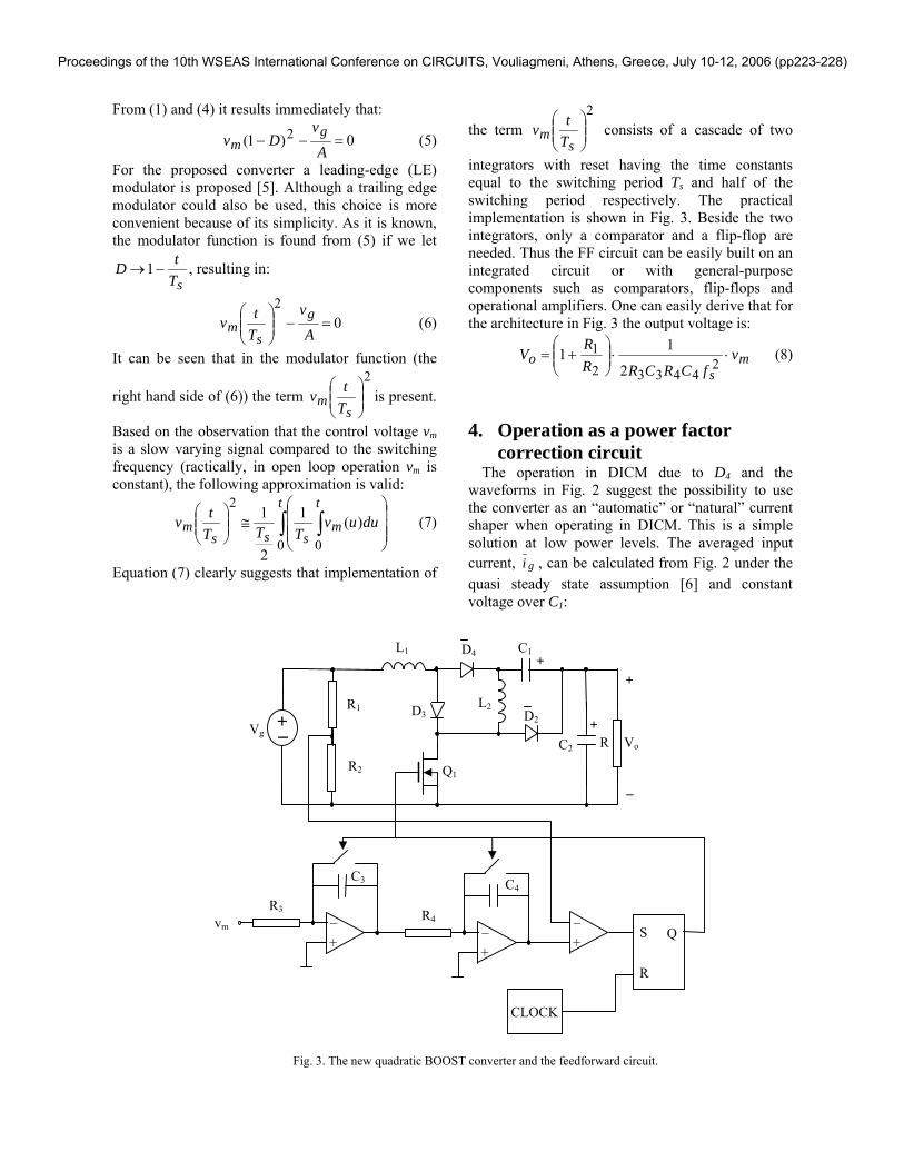
integrators with reset having the time constants equal to the switching period Ts and half of the switching period respectively. The practical implementation is shown in Fig. 3. Beside the two integrators, only a comparator and a flip-flop are needed. Thus the FF circuit can be easily built on an integrated circuit or with general-purpose components such as comparators, flip-flops and operational amplifiers. One can easily derive that for the architecture in Fig. 3 the output voltage is:
ms
o vfCRCRR
RV ⋅⋅⎟⎟
⎠
⎞⎜⎜⎝
⎛+=
244332
12
11 (8)
4. Operation as a power factor correction circuit
The operation in DICM due to D4 and the waveforms in Fig. 2 suggest the possibility to use the converter as an “automatic” or “natural” current shaper when operating in DICM. This is a simple solution at low power levels. The averaged input current, gi , can be calculated from Fig. 2 under the quasi steady state assumption [6] and constant voltage over C1:
L1 C1
D2D3
C2 R
Q1
Vo
Fig. 3. The new quadratic BOOST converter and the feedforward circuit.
Vg
+
+
D4
L2
+ _
+
_
R1
R2
+
_
+
_
+
_ Q S
R
vm
CLOCK
R3
C3
R4
C4
Proceedings of the 10th WSEAS International Conference on CIRCUITS, Vouliagmeni, Athens, Greece, July 10-12, 2006 (pp223-228)
tVV
VR
vi
CoMe
gg
ωsin1
1
1−
−⋅= (9)
where the emulated resistance is:
212
D
fLR s
e = (10)
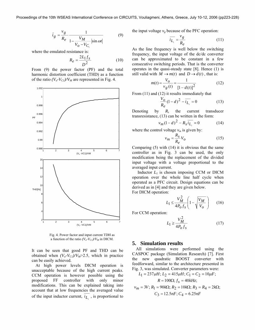
From (9) the power factor (PF) and the total harmonic distortion coefficient (THD) as a function of the ratio (Vo-VC1)/VM are represented in Fig. 4.
It can be seen that good PF and THD can be obtained when (Vo-VC1)/VM>2.5, which in practice can be easily achieved.
At high power levels DICM operation is unacceptable because of the high current peaks. CCM operation is however possible using the proposed FF controller with only minor modifications. This can be explained taking into account that at low frequencies the averaged value of the input inductor current,
1Li , is proportional to
the input voltage vg because of the PFC operation:
e
gL R
vi =
1 (11)
As the line frequency is well below the switching frequency, the input voltage of the dc/dc converter can be approximated to be constant in a few consecutive switching periods. That is the converter operates in the quasi-steady state [8]. Hence (1) is still valid with )(tmM → and )(tdD → , that is:
2)](1[
1)(
)(tdtv
Vtm
go
−== (12)
From (11) and (12) it results immediately that
0)1(1
2 =−− Leo id
RV
(13)
Denoting by Rs the current transducer transresistance, (13) can be written in the form:
0)1(1
2 =−− Lsm iRdv (14)
where the control voltage vm is given by:
oes
m VRR
v = (15)
Comparing (5) with (14) it is obvious that the same controller as in Fig. 3 can be used, the only modification being the replacement of the divided input voltage with a voltage proportional to the averaged input current. Inductor L1 is chosen imposing CCM or DICM operation over the whole line half cycle when operated as a PFC circuit. Design equations can be derived as in [4] and they are given below. For DICM operation:
⎟⎟⎠
⎞⎜⎜⎝
⎛−≤
oM
soM
VV
fPV
L 14
2
1 (16)
For CCM operation:
soM
fPV
L4
2
1 ≥ (17)
5. Simulation results
All simulations were performed using the CASPOC package (Simulation Research) [7]. First the new quadratic BOOST converter with feedforward, similar to the architecture presented in Fig. 3, was simulated. Converter parameters were:
nFCnFCkRRkRkRVv
kHzfRFCCHLHL
m
s
25.6;5.12;2;10;90;3
;40;100;10;415;237
43
4321
2121
==Ω==Ω=Ω==
=Ω===== μμμ
Fig. 4. Power factor and input current TDH as a function of the ratio (Vo-VC1)/VM in DICM.
1 2 3 4 5 6 70.988
0.99
0.992
0.994
0.996
0.998
1
1.002
(Vo -VC1)/VM
PF
(Vo- VC1)/VM 1 2 3 4 5 6 7
2
4
6
8
10
12
14
16
THD[%]
Proceedings of the 10th WSEAS International Conference on CIRCUITS, Vouliagmeni, Athens, Greece, July 10-12, 2006 (pp223-228)

The input voltage was forced to vary with a square waveshape between 8V and 14 V. The simulation results are shown in Fig. 5. It can be seen that after
short transients the output voltage tightly follows the prescribed 30V value.
Then the converter was simulated in a PFC application with DICM operation. The parameters of the PFC circuit were:
;2.0;40;100;400;40;470;1;5.0;6.30;70
2
121
==Ω====
====
DkHzfRVVWPFC
FCmHLHLVV
s
oo
Mμ
μμ
After the uncontrolled bridge supplying the converter, a small high frequency filter with LF=80μH and CF=2μF was used, in order to suppress the high frequency components from the input current which are large in DICM. In Fig. 6 the input voltage and current waveforms are presented. The expected output voltage of 800 V was confirmed by the simulation which provided an output voltage of 806 V. It can be seen that qualitatively the input current has a closely sinusoidal shape and tightly follows the input voltage. The input current total harmonic distortion (THD) coefficient was 2.4%, while unity displacement power factor was found. An excellent total power factor of 0.998 was achieved. In order to verify the feasibility of a PFC circuit
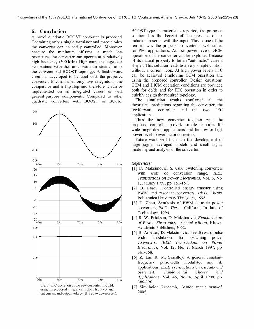
using the new quadratic converter operated in CCM, a PFC circuit employing the same controller structure as that in Fig. 3, but using the input inductor current as the second input was simulated. The circuit parameters were the following:
VvkHzfRVVWPFC
FCHLHLVV
ms
oo
M
8.2;40;160;400;1000;2200;1;400;250;7.169
2
121
==Ω====
====μ
μμμ
As the converter is CCM operated, no additional high frequency filter is needed. The simulated waveforms are shown in Fig. 7, qualitatively revealing excellent operation. The resulted average output voltage was 398V, in accordance to the theoretical considerations. The input current exhibited a THD of 9.2% and the total power factor of the system was 0.995.
5
10
15
0
20
60m 70m 80m 90m 100m 110m 120m
10
20
30
0
40
60m 70m 80m 90m 100m 110m 120m
Fig. 5. Dynamic operation of the quadratic BOOST converter with FF. Input voltage (up) and output
voltage (down).
40
-40
-80
80
40m 45m 50m 55m 60m
1
2
-1
-2
-3
3
40m 45m 50m 55m 60m
200
400
0
500
40m 45m 50m 55m 60m Fig. 6. PFC operation of the new converter in DICM mode. Input voltage, input current and
output voltage (this up to down order).
0
Proceedings of the 10th WSEAS International Conference on CIRCUITS, Vouliagmeni, Athens, Greece, July 10-12, 2006 (pp223-228)
6. Conclusion A novel quadratic BOOST converter is proposed. Containing only a single transistor and three diodes, the converter can be easily controlled. Moreover, because the minimum off-time is much less restrictive, the converter can operate at a relatively high frequency (500 kHz). High output voltages can be obtained with the same transistor stresses as in the conventional BOOST topology. A feedforward circuit is developed to be used with the proposed converter. It consists of only two integrators, one comparator and a flip-flop and therefore it can be implemented on an integrated circuit or with general-purpose components. Compared to other quadratic converters with BOOST or BUCK-
BOOST type characteristics reported, the proposed solution has the benefit of the presence of an inductor in series with the input. This is one of the reasons why the proposed converter is well suited for PFC applications. At low power levels DICM operation of the converter can be exploited because of its natural property to be an “automatic” current shaper. This solution leads to a very simple control, without a current loop. At high power levels PFC can be achieved employing CCM operation and using the proposed controller. Design equations, CCM and DICM operation conditions are provided both for dc/dc and for PFC operation in order to quickly design the required topology.
The simulation results confirmed all the theoretical predictions regarding the converter, the feedforward controller and the two PFC applications.
Thus the new converter together with the proposed controller provide simple solutions for wide range dc/dc applications and for low or high power levels power factor correctors.
Future work will focus on the development of large signal averaged models and small signal modeling and analysis of the converter. References: [1] D. Maksimović, S. Ćuk, Switching converters
with wide dc conversion range, IEEE Transactions on Power Electronics, Vol. 6, No. 1, January 1991, pp. 151-157.
[2] D. Lascu, Controlled energy transfer using PWM and resonant converters, Ph.D. Thesis, Politehnica University Timişoara, 1998.
[3] D. Zhou, Synthesis of PWM dc-to-dc power converters, Ph.D. Thesis, California Institute of Technology, 1996.
[4] R. W. Erickson, D. Maksimović, Fundamentals of Power Electronics - second edition, Kluwer Academic Publishers, 2002.
[5] B. Arbetter, D. Maksimović, Feedforward pulse width modulators for switching power converters, IEEE Transactions on Power Electronics, Vol. 12, No. 2, March 1997, pp. 361-368.
[6] Z. Lai, K. M. Smedley, A general constant-frequency pulsewidth modulator and its applications, IEEE Transactions on Circuits and Systems-I: Fundamental Theory and Applications, Vol. 45, No. 4, April 1998, pp. 386-396.
[7] Simulation Research, Caspoc user’s manual, 2005.
100
-100
-200
200
60m 65m 70m 75m
200
400
0
500
60m 65m 70m 75m 80m
5
10
15
-5
-10
-15
-20
20
60m 65m 70m 75m 80m
80m
Fig. 7. PFC operation of the new converter in CCM, using the proposed integral controller. Input voltage,
input current and output voltage (this up to down order).
Proceedings of the 10th WSEAS International Conference on CIRCUITS, Vouliagmeni, Athens, Greece, July 10-12, 2006 (pp223-228)


![Bridgeless Buck-Boost PFC Converter for Multistring LED Driver€¦ · boost converter as a universal PFC converter [6]. In order to address these issues, a buck-boost converter is](https://static.fdocuments.in/doc/165x107/5eaabf2a4ab79d1e774f9005/bridgeless-buck-boost-pfc-converter-for-multistring-led-driver-boost-converter-as.jpg)


