Boost PFC Converter Control Loop Design - PSIM … · Boost PFC Converter Control Loop Design - 4 -...
27
Boost PFC Converter Control Loop Design Tutorial –April 2016-
Transcript of Boost PFC Converter Control Loop Design - PSIM … · Boost PFC Converter Control Loop Design - 4 -...

Boost PFC Converter Control Loop Design
Tutorial –April 2016-

How to Contact:
www.powersmartcontrol.com
This SmartCtrl© Tutorial by Carlos III University is licensed under a Creative Commons Attribution 4.0
International License:
You are free to:
Share — copy and redistribute the material in any medium or format
Adapt — remix, transform, and build upon the material for any purpose, even commercially.
The licensor cannot revoke these freedoms as long as you follow the license terms.
Under the following terms:
Attribution — You must give appropriate credit, provide a link to the license, andindicate if
changes were made. You may do so in any reasonable manner, but not in any way that suggests
the licensor endorses you or your use.
No additional restrictions — You may not apply legal terms or technological measures that
legally restrict others from doing anything the license permits.
Based on a work at www.powersmartcontrol.com
SmartCtrl© 2009-2016 by Carlos III University of Madrid. GSEP Power Electronics Systems Group
The software SmartCtrl© described in this manual is furnished under a license agreement. The software may be used or
copied only under the terms of the license agreement.

Boost PFC Converter Control Loop Design
- 2 -
Boost PFC Converter Control Loop Design Tutorial V2.0 – April 2016 www.powersmartcontrol.com
Table of contents
1. Introduction ............................................................ 3
2. Inner Loop Design .................................................. 5
3. Outer Loop Design .............................................. 14
4. Design results ...................................................... 18
Boost PFC Converter Control Loop Design
- 3 -
Boost PFC Converter Control Loop Design Tutorial V2.0 – April 2016 www.powersmartcontrol.com
1. Introduction
SmartCtrl1 is a general-purpose controller design software specifically for power
electronics applications. This tutorial is intended to guide you, step by step, to
design the control loops of a PFC (power factor correction) boost converter with
the SmartCtrl Software.
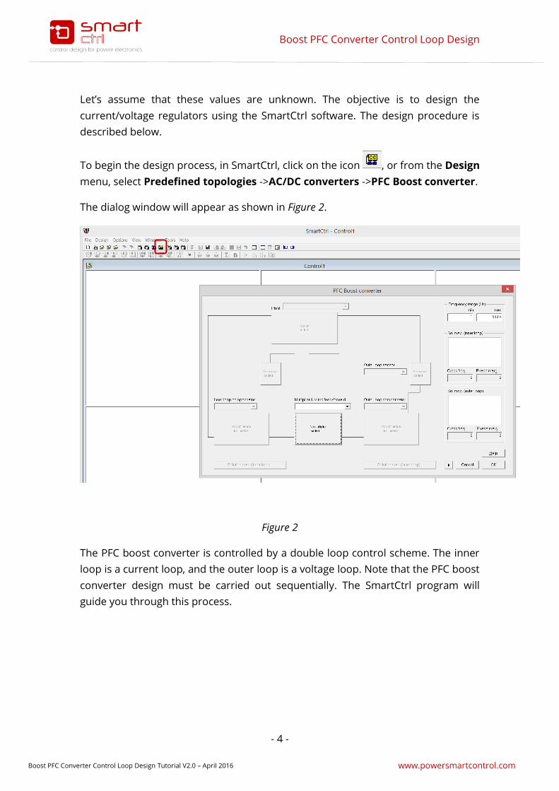
The example used in this tutorial is the PFC boost converter circuit that comes with
the PSIM example set. The PSIM schematic is shown in Figure 1.
Figure 1
The circuit includes the inner current loop and the outer voltage loop. The current
loop regulator parameters are the resistance Rcz and the capacitances Ccz and
Ccp, and the voltage regulator parameters are the resistance RVF and the
capacitance CVF, highlighted in the red dotted boxes above.
1SmartCtrl is copyright in 2009-2011 by Carlos III University of Madrid, GSEP Power Electronics
Systems Group, Spain
Current regulator:INNER LOOP
Voltage regulator:OUTER LOOP
Boost PFC Converter Control Loop Design
- 4 -
Boost PFC Converter Control Loop Design Tutorial V2.0 – April 2016 www.powersmartcontrol.com
Let’s assume that these values are unknown. The objective is to design the
current/voltage regulators using the SmartCtrl software. The design procedure is
described below.
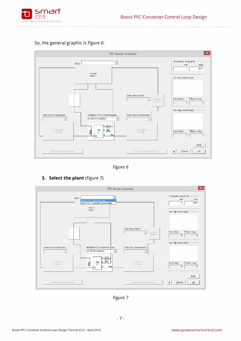
To begin the design process, in SmartCtrl, click on the icon , or from the Design
menu, select Predefined topologies ->AC/DC converters ->PFC Boost converter.
The dialog window will appear as shown in Figure 2.
Figure 2
The PFC boost converter is controlled by a double loop control scheme. The inner
loop is a current loop, and the outer loop is a voltage loop. Note that the PFC boost
converter design must be carried out sequentially. The SmartCtrl program will
guide you through this process.

Boost PFC Converter Control Loop Design
- 5 -
Boost PFC Converter Control Loop Design Tutorial V2.0 – April 2016 www.powersmartcontrol.com
2. Inner Loop Design
Before designing the inner loop, select the type of the multiplier.
1. Select the Multiplier (Figure 3)
Figure 3
In this case, select the UC3854A according to the schematic circuit ¡Error! No se e
ncuentra el origen de la referencia..
Attending to the schematic in Figure 1, the parameters of the multiplier for this
particular example are the ones shown in Figure 4. Notice that KFF, the feed-
forward gain, is the ratio between the rms input voltage and the average input
voltage to the multiplier. It has been calculated applying (1):
𝐾𝐹𝐹 = √2 ·2
𝜋·
𝑅𝐹𝐹3
𝑅𝐹𝐹1+𝑅𝐹𝐹2+𝑅𝐹𝐹3 (1)
RFF1, RFF2, RFF3, Rac y Rmo are the resistances with the same name in the
schematic in Figure 1.

Boost PFC Converter Control Loop Design
- 6 -
Boost PFC Converter Control Loop Design Tutorial V2.0 – April 2016 www.powersmartcontrol.com
Figure 4
2. Select the gain of the inner loop sensor ( Figure 5)
Select a constant gain election of the current sensor Rs. It is a resistor and it is
represented in the picture of the power plant (Figure 8).
Figure 5
Boost PFC Converter Control Loop Design
- 7 -
Boost PFC Converter Control Loop Design Tutorial V2.0 – April 2016 www.powersmartcontrol.com
So, the general graphic is Figure 6:
Figure 6
3. Select the plant (Figure 7).
Figure 7
Boost PFC Converter Control Loop Design
- 8 -
Boost PFC Converter Control Loop Design Tutorial V2.0 – April 2016 www.powersmartcontrol.com
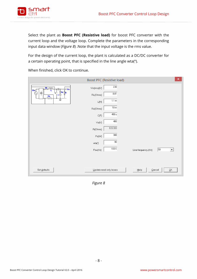
Select the plant as Boost PFC (Resistive load) for boost PFC converter with the
current loop and the voltage loop. Complete the parameters in the corresponding
input data window (Figure 8) .Note that the input voltage is the rms value.
For the design of the current loop, the plant is calculated as a DC/DC converter for
a certain operating point, that is specified in the line angle wta(º).
When finished, click OK to continue.
Figure 8

Boost PFC Converter Control Loop Design
- 9 -
Boost PFC Converter Control Loop Design Tutorial V2.0 – April 2016 www.powersmartcontrol.com
4. Select the current regulator (Figure 9).
Figure 9
From the inner loop regulator drop-down menu, select “Type 2” as the current
regulator type. It is necessary to know the ramp waveform in order to specify the
parameters Vmaxt (maximum voltage), Vmint (minimum voltage) and tr (rise time).
The parameters in Figure 10 correspond to the simulation of the schematic in
Figure 9, which provides the ramp waveform depicted in Figure 11.

Boost PFC Converter Control Loop Design
- 10 -
Boost PFC Converter Control Loop Design Tutorial V2.0 – April 2016 www.powersmartcontrol.com
Figure 10
¡Error! No se encuentra el o
rigen de la referencia.

Boost PFC Converter Control Loop Design
- 11 -
Boost PFC Converter Control Loop Design Tutorial V2.0 – April 2016 www.powersmartcontrol.com
5. Select the crossover frequency and the phase margin (Figure 11).
Figure 11
SmartCtrl provides a guideline and an easy way of selecting the crossover
frequency and the phase margin through the Solution Map. Click on the Set
button, and the Solution Map will be shown (Figure 12).

Boost PFC Converter Control Loop Design
- 12 -
Boost PFC Converter Control Loop Design Tutorial V2.0 – April 2016 www.powersmartcontrol.com
Figure 12
In the Solution Map, each point within the white area corresponds to a
combination of the crossover frequency and the phase margin that leads to a
stable solution. In addition, when a point is selected, the attenuation given by the
sensor and the regulator at the switching frequency is provided.
To carry out the selection, left click a point within the white area, or enter the
crossover frequency and the phase margin manually.
Once the crossover frequency and the phase margin are selected, the Solution
Map will be shown on the right side of the converter input window. If, at any time,
it is required to change the crossover frequency or the phase margin, click on the
white area of the Solution Map, as shown in Figure 11.

Boost PFC Converter Control Loop Design
- 13 -
Boost PFC Converter Control Loop Design Tutorial V2.0 – April 2016 www.powersmartcontrol.com
Figure 13

Boost PFC Converter Control Loop Design
- 14 -
Boost PFC Converter Control Loop Design Tutorial V2.0 – April 2016 www.powersmartcontrol.com
3. Outer Loop Design
The procedure of designing the outer loop is similar to that of the inner loop
design.
1. Select the voltage sensor (Figure 14)
Figure 14
When using a voltage divider, one must enter the reference voltage, and the
program will automatically calculate the sensor gain.
However, in this particular example, the option is a “Regulator embedded voltage
divider”.
Boost PFC Converter Control Loop Design
- 15 -
Boost PFC Converter Control Loop Design Tutorial V2.0 – April 2016 www.powersmartcontrol.com
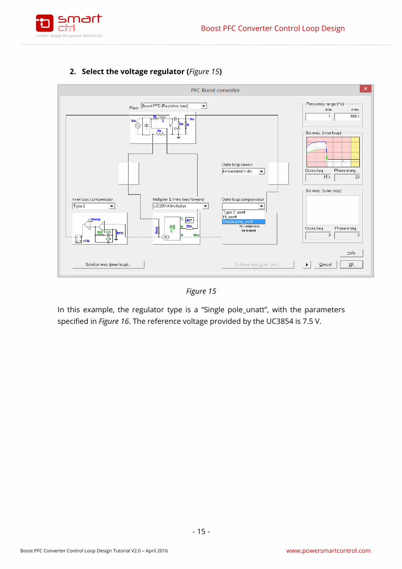
2. Select the voltage regulator (Figure 15)
Figure 15
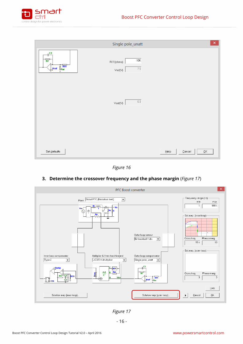
In this example, the regulator type is a “Single pole_unatt”, with the parameters
specified in Figure 16. The reference voltage provided by the UC3854 is 7.5 V.
Boost PFC Converter Control Loop Design
- 16 -
Boost PFC Converter Control Loop Design Tutorial V2.0 – April 2016 www.powersmartcontrol.com
Figure 16
3. Determine the crossover frequency and the phase margin (Figure 17)
Figure 17

Boost PFC Converter Control Loop Design
- 17 -
Boost PFC Converter Control Loop Design Tutorial V2.0 – April 2016 www.powersmartcontrol.com
The crossover frequency and the phase margin of the outer loop must be selected.
A Solution Map is also provided to help select a stable solution. Press the Solution
map (outer loop) button and the solution map will appear (Figure 18 ). Then select a
point by clicking within the white area, and click OK to continue.
Figure 18
Once the crossover frequency and the phase margin are selected, the Solution
Map will appear on the right side of the converter input window. If, at any time,
these two parameters need to be changed, click in the white area of the Solution
Map, as shown in Figure 19.

Boost PFC Converter Control Loop Design
- 18 -
Boost PFC Converter Control Loop Design Tutorial V2.0 – April 2016 www.powersmartcontrol.com
Figure 19
Accept the selected design by clicking on OK. The program will automatically show
the control system performance by means of the Bode plots, the Nyquist plot,
phase margin, etc.
4. Design results
SmartCtrl provides the regulator component values needed to implement the
regulators, as well as the voltage divider resistors (“Output data” in Figure 20). Since
there are two control loops, one must select which one to display (Figure 20Figure
20)

Boost PFC Converter Control Loop Design
- 19 -
Boost PFC Converter Control Loop Design Tutorial V2.0 – April 2016 www.powersmartcontrol.com
Figure 20
The Bode plots and Nyquist plot corresponding to the outer loop are shown in
Figure 21, as well as the graphical information regarding the inner loop is shown in
Figure 22. In the right panel “Method”, two parameters appear:
Attenuation (fsw)(dB). This is the attenuation in dB achieved by the open
loop transfer function at the switching frequency. It should be low for the
inner loop and the outer loop.
Loop gain (2fl)(dB) . This is the attenuation in dB achieved by the open loop
transfer function at twice the line frequency (100 Hz or 120 Hz). It should be
high for the inner loop and low for the outer loop.
By clicking with the right button on the line current panel, a floating menu appears,
offering different choices. One of them is the command FFT, which displays a new
window with a plot that shows the amplitude of the first and third harmonics of
the line current, to provide more information regarding the harmonic distortion.
Display inner
loop
Display outer
loop
Output data
Display inner
loop
Display outer
loop

Boost PFC Converter Control Loop Design
- 20 -
Boost PFC Converter Control Loop Design Tutorial V2.0 – April 2016 www.powersmartcontrol.com
Figure 21
Figure 22
Red dot
Blue dot

Boost PFC Converter Control Loop Design
- 21 -
Boost PFC Converter Control Loop Design Tutorial V2.0 – April 2016 www.powersmartcontrol.com
The red dot in the rectified line voltage plot (Figure 22) originally corresponds to the
line angle wta specified in the plant window (Figure 8). This dot can be moved by
clicking and dragging, and the Bode plot and the attenuation parameters will
refresh, as the plant is recalculated considering the equivalent DC/DC converter for
that particular operating point. An example is depicted in Figure 23, modifying the
line angle. Notice how the open-loop gain varies.

Boost PFC Converter Control Loop Design
- 22 -
Boost PFC Converter Control Loop Design Tutorial V2.0 – April 2016 www.powersmartcontrol.com
wta = 90o wta = 45o wta = 30o
Figure 23
The blue dot in the rectified line voltage plot (Figure 22) is placed in the line angle
that corresponds to the maximum current ripple through the inductor. Some
results obtained by simulating the schematic in Figure 1 are depicted in Figure 24,
to illustrate the meaning of this blue dot. In the left part of Figure 24, the voltage at
the output of the rectifier and the current through the inductor are shown,
indicating the position of the blue dot. In the right part of the figure, a detail of the
same waveforms is shown, as well as the oscillator ramp and the internal
compensator output. PSIM results (lower part of Figure 24) can be compared with
SmartCrtl results (¡Error! No se encuentra el origen de la referencia.) for the
same line angle.
The plot that shows the oscillator ramp and the inner compensator output is
useful to determine whether there could be oscillations. If the slopes of both

Boost PFC Converter Control Loop Design
- 23 -
Boost PFC Converter Control Loop Design Tutorial V2.0 – April 2016 www.powersmartcontrol.com
functions are too similar, there could be more than one intersection per period,
causing oscillations.
Figure 24
Inductor current
Oscillator ramp
PSIM

Boost PFC Converter Control Loop Design
- 24 -
Boost PFC Converter Control Loop Design Tutorial V2.0 – April 2016 www.powersmartcontrol.com
When a single-pole is used as the compensator type of the outer loop, there are
some advantages regarding the line current distortion. On the other hand, the
actual output voltage may not be exactly the specified due to the low gain at low
frequency (see Bode plot gain in Figure 21), causing some differences between the
SmartCtrl results and the simulated results. However, if the actual output voltage is
10% higher than the specified one, SmartCtrl will provide a warning message,
recommending the user to check this point and increase low frequency gain.In this
particular example, the actual output voltage is 415 V instead the specified 400 V,
and consequently there is not any warning message.
Table1
Original design New design
Inner loop (type 2) fc=15 kHz
PM=60º
Inner loop (type 2) fc=15 kHz
PM=60º
Outer loop (single-
pole)
fc=25 Hz
PM=40º
Outer loop (single-
pole)
fc=15 Hz
PM=60º
Specified output
voltage
400 V Specified output
voltage
400 V
Actual output voltage 415 V Actual output
voltage
448 V

Boost PFC Converter Control Loop Design
- 25 -
Boost PFC Converter Control Loop Design Tutorial V2.0 – April 2016 www.powersmartcontrol.com
To illustrate this problem related with the low gain of the outer loop at low
frequency, a new outer loop has been design, with different phase margin (PM)
and cross-over frequency (fc). The comparison between this design and the
original one can be found in Table1. The new design has a lower gain at low
frequency and the measured output voltage is 448 V, that is, more than 10% higher
than the specified value.
Regarding the inner control loop, it is very important to consider that it is
necessary to have a high enough bandwidth in order to follow the rectified
sinusoidal reference. If the cross-frequency of the current loop is not high enough,
a zero-crossing distortion in the input current will happen. In these occasions, the
results provided by SmartCtrl may not match the actual results, as the line current
Open-loop gain at 1 Hz=28.14 dBOpen-loop gain at 1 Hz=18.56 dB

Boost PFC Converter Control Loop Design
- 26 -
Boost PFC Converter Control Loop Design Tutorial V2.0 – April 2016 www.powersmartcontrol.com
waveform is calculated by SmartCtrlassuming that the current loop follows
perfectly well the reference generated by the outer loop. Consequently, when a
zero-crossing distortion is expected, the program displays a warning message to
inform the user thatthe actual line current would differ from the one represented.
The cross-frequency of the inner loop compensator should be increased to
minimize this problem.
To illustrate this problem related with the low cross-over frequency of the inner
loop, a comparison between several designs of the inner loop with different phase
margin (PM) and cross-over frequency (fc). The input current waveforms achieved
with these designs are compared in ¡Error! No se encuentra el origen de la
referencia..Notice the important zero-crossing distortion for cross-over frequency
lower than 5 kHz, and how the distortion is minimized as the cross-frequency is
increased.
fc=1 kHzPM=60º
fc=3 kHzPM=60º
fc=5 kHzPM=60º
fc=4 kHzPM=60º
fc=15 kHzPM=60º
fc=10 kHzPM=60º