Semiconductors and PN junction 1. Explain PN junction diode. · 2018-10-06 · 1 Mrs. V. S....
20
1 Mrs. V. S. Patki(Electronics Department) Walchand Institute of Technology, Solapur Semiconductors and PN junction 1. Explain PN junction diode. When a p-type semiconductor material is suitably joined to n-type semiconductor the contact surface is called a p-n junction. The p-n junction is also called as semiconductor diode. • The left side material is a p-type semiconductor having –ve acceptor ions and +vely charged holes. The right side material is n-type semiconductor having +ve donor ions and free electrons. • Suppose the two pieces are suitably treated to form pn junction, then there is a tendency for the free electrons from n-type to diffuse over to the p-side and holes from p-type to the n-side . This process is called diffusion. No external voltage is applied between the terminals of PN junction, hence the pn junction is called unbiased. •Due to charge concentration difference (Potential gradient) the free electrons move across the junction from n-type to p-type, +ve donor ions are formed in . Hence a +ve charge is built on the n-side of the junction. At the same time, the free electrons cross the junction and form the –ve acceptor ions by filling in the holes. Therefore a net –ve charge is established on p-side of the junction. • When a sufficient number of donor and acceptor ions are formed further diffusion is prevented. At this point the junction is said to have attained an equilibrium. • Thus a barrier is set up against further movement of charge carriers. This is called potential barrier or junction barrier or cut in voltage Vo. The potential barrier for si is 0.7 volts and for Ge is 0.3 volts. Note: outside this barrier on each side of the junction, the material is still neutral. Only inside the barrier, there is a +ve charge on n-side and –ve charge on p-side. This region is called depletion layer. The shaded portion on both sides of junction contains only immobile ions and not charge carriers such as electrons or holes. In other words region is depleted of charge carriers.
Transcript of Semiconductors and PN junction 1. Explain PN junction diode. · 2018-10-06 · 1 Mrs. V. S....
1 Mrs. V. S. Patki(Electronics Department) Walchand Institute of Technology, Solapur
Semiconductors and PN junction
1. Explain PN junction diode.
When a p-type semiconductor material is suitably joined to n-type semiconductor the contact surface is
called a p-n junction. The p-n junction is also called as semiconductor diode.
•
The left side material is a p-type semiconductor having –ve acceptor ions and +vely charged holes. The
right side material is n-type semiconductor having +ve donor ions and free electrons.
• Suppose the two pieces are suitably treated to form pn junction, then there is a tendency for the free
electrons from n-type to diffuse over to the p-side and holes from p-type to the n-side . This process is
called diffusion.
No external voltage is applied between the terminals of PN junction, hence the pn junction is
called unbiased.
•Due to charge concentration difference (Potential gradient) the free electrons move across the junction
from n-type to p-type, +ve donor ions are formed in . Hence a +ve charge is built on the n-side of the
junction. At the same time, the free electrons cross the junction and form the –ve acceptor ions by
filling in the holes. Therefore a net –ve charge is established on p-side of the junction.
• When a sufficient number of donor and acceptor ions are formed further diffusion is prevented.
At this point the junction is said to have attained an equilibrium.
• Thus a barrier is set up against further movement of charge carriers. This is called potential barrier
or junction barrier or cut in voltage Vo. The potential barrier for si is 0.7 volts and for Ge is 0.3 volts.
Note: outside this barrier on each side of the junction, the material is still neutral. Only inside the
barrier, there is a +ve charge on n-side and –ve charge on p-side. This region is called depletion layer.
The shaded portion on both sides of junction contains only immobile ions and not charge carriers
such as electrons or holes. In other words region is depleted of charge carriers.
2 Mrs. V. S. Patki(Electronics Department) Walchand Institute of Technology, Solapur
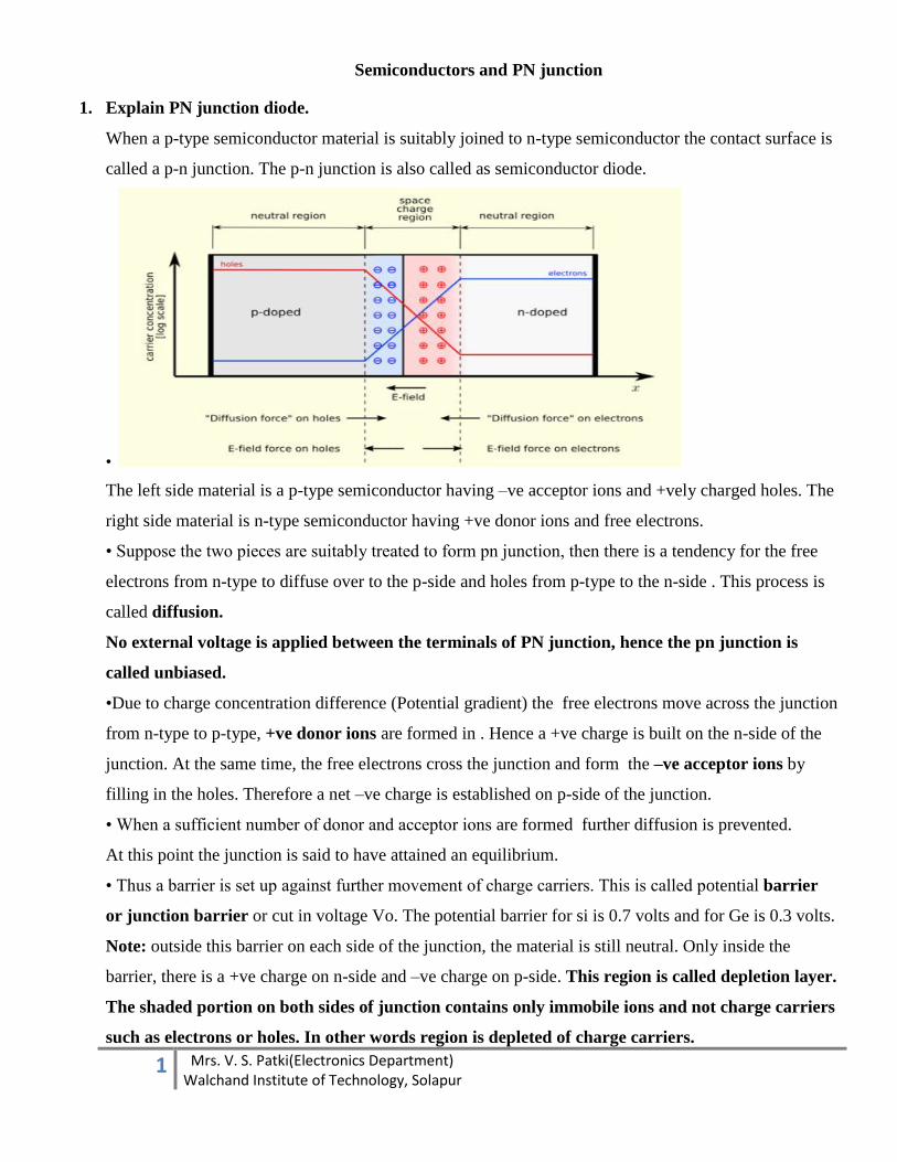
Depletion Region
In the p-type region there are holes from the acceptor impurities and in the n-
type region there are extra electrons.
When a p-n junction is formed, some of the electrons from the n-region which
have reached the conduction band are free to diffuse across the junction and
combine with holes.
Filling a hole makes a negative ion and leaves behind a positive ion on the n-
side. A space charge builds up, creating a depletion region which inhibits any
further electron transfer unless it is helped by putting a forward bias on the
junction.
Energy band diagram for Equilibrium of junction
Potential Barrier
The electric field formed in the depletion region acts as a barrier. Barrier Potential in a PN junction
refers to the potential required to overcome the barrier at the PN junction.
External energy must be applied to get the electrons to move across the barrier of the electric field.
The potential difference required to move the electrons through the electric field is called the barrier
potential.
Barrier potential of a PN junction depends on the type of semiconductor material, amount of doping
and temperature.
This is approximately 0.7V for silicon and 0.3V for germanium.
2. Explain Biasing of PN junction diode.
Connecting a p-n junction to an external d.c. voltage source is called biasing.
1.Forward biasing 2.Reverse biasing
3 Mrs. V. S. Patki(Electronics Department) Walchand Institute of Technology, Solapur
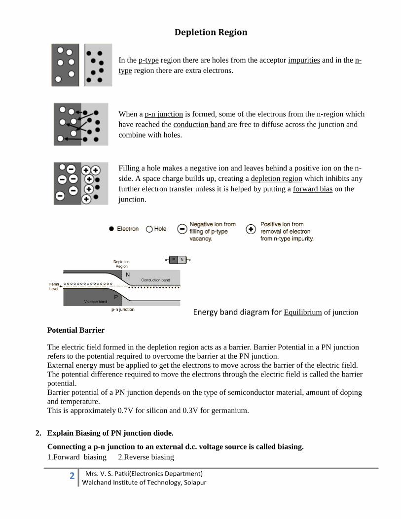
1.Forward biasing
• When external voltage applied to the junction
is in such a direction that it cancels the
potential barrier, thus permitting current flow
is called forward biasing i.e. P-region is
connected to positive terminal and N-region is
connected to negative terminal of source.
• To apply forward bias, connect +ve terminal
of the battery to p-type and –ve terminal to n-
type as shown in fig. below.
• The applied forward potential establishes the
electric field which acts against the field due to
potential barrier. Therefore the resultant field is weakened and the barrier height is reduced at the
junction as shown in fig.
• Due to negative terminal of the battery free electrons from n side are pushed towards the p-side and
due to positive terminal of the battery holes are pushed towards n-side.
Since the potential barrier voltage is very small, a small forward voltage is sufficient to completely
eliminate the barrier. Once the potential barrier is eliminated by the forward voltage, junction resistance
becomes almost zero and a low resistance path is established for the entire circuit. Therefore current
flows in the circuit. This is called forward current.
Energy band diagram for forward bias
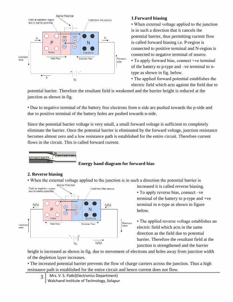
2. Reverse biasing
• When the external voltage applied to the junction is in such a direction the potential barrier is
increased it is called reverse biasing.
• To apply reverse bias, connect –ve
terminal of the battery to p-type and +ve
terminal to n-type as shown in figure
below.
• The applied reverse voltage establishes an
electric field which acts in the same
direction as the field due to potential
barrier. Therefore the resultant field at the
junction is strengthened and the barrier
height is increased as shown in fig. due to movement of electrons and holes away from junction width
of the depletion layer increases.
• The increased potential barrier prevents the flow of charge carriers across the junction. Thus a high
resistance path is established for the entire circuit and hence current does not flow.
4 Mrs. V. S. Patki(Electronics Department) Walchand Institute of Technology, Solapur
Energy band diagram for Reverse bias
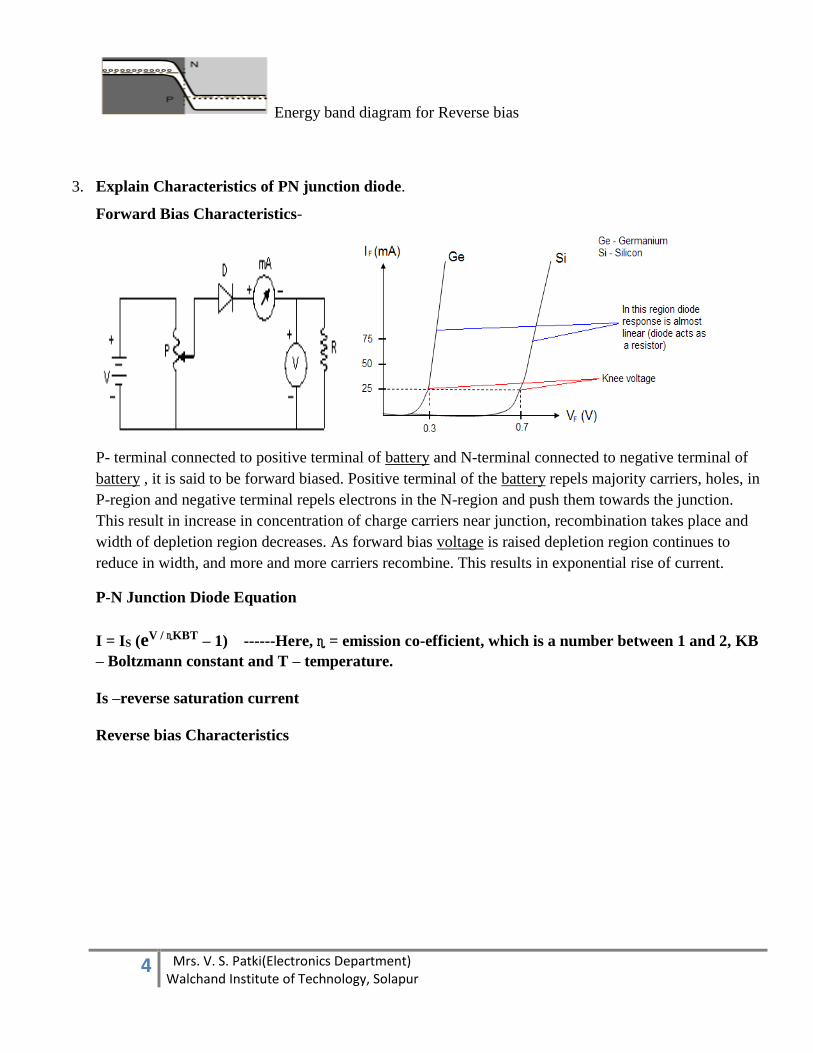
3. Explain Characteristics of PN junction diode.
Forward Bias Characteristics-
P- terminal connected to positive terminal of battery and N-terminal connected to negative terminal of
battery , it is said to be forward biased. Positive terminal of the battery repels majority carriers, holes, in
P-region and negative terminal repels electrons in the N-region and push them towards the junction.
This result in increase in concentration of charge carriers near junction, recombination takes place and
width of depletion region decreases. As forward bias voltage is raised depletion region continues to
reduce in width, and more and more carriers recombine. This results in exponential rise of current.
P-N Junction Diode Equation
I = IS (eV / ɳKBT – 1) ------Here, ɳ = emission co-efficient, which is a number between 1 and 2, KB
– Boltzmann constant and T – temperature.
Is –reverse saturation current
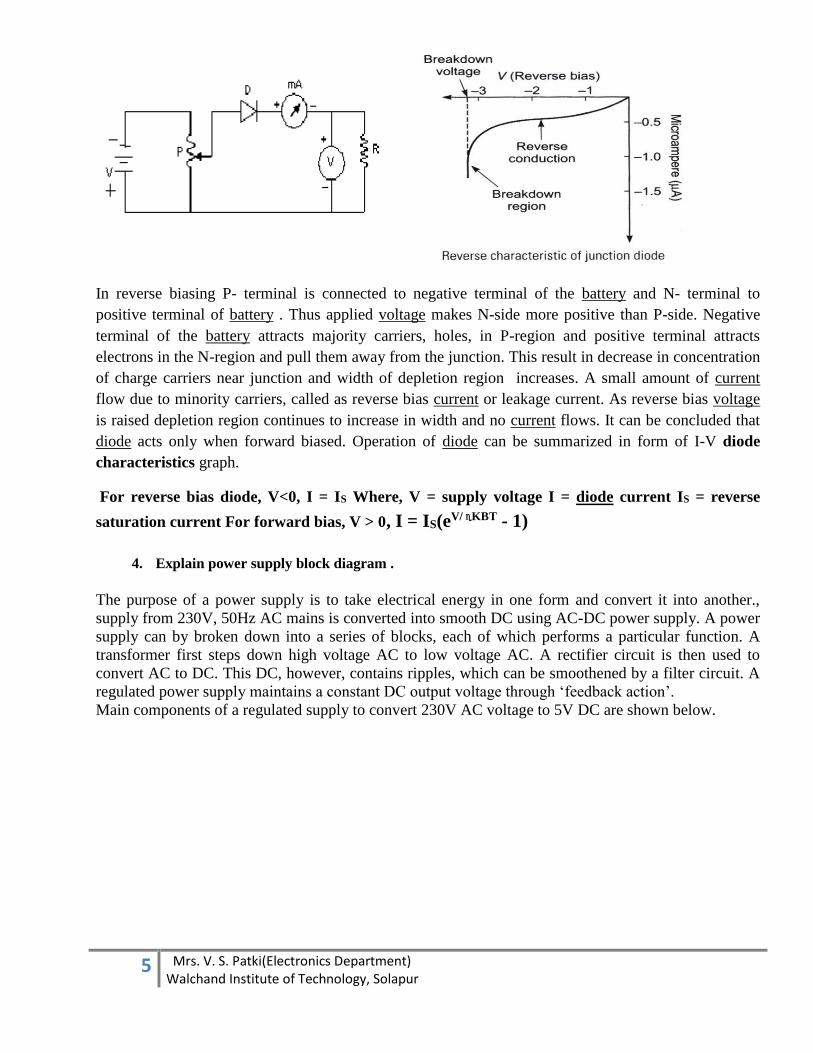
Reverse bias Characteristics
5 Mrs. V. S. Patki(Electronics Department) Walchand Institute of Technology, Solapur
In reverse biasing P- terminal is connected to negative terminal of the battery and N- terminal to
positive terminal of battery . Thus applied voltage makes N-side more positive than P-side. Negative
terminal of the battery attracts majority carriers, holes, in P-region and positive terminal attracts
electrons in the N-region and pull them away from the junction. This result in decrease in concentration
of charge carriers near junction and width of depletion region increases. A small amount of current
flow due to minority carriers, called as reverse bias current or leakage current. As reverse bias voltage
is raised depletion region continues to increase in width and no current flows. It can be concluded that
diode acts only when forward biased. Operation of diode can be summarized in form of I-V diode
characteristics graph.
For reverse bias diode, V<0, I = IS Where, V = supply voltage I = diode current IS = reverse
saturation current For forward bias, V > 0, I = IS(eV/ ɳKBT - 1)
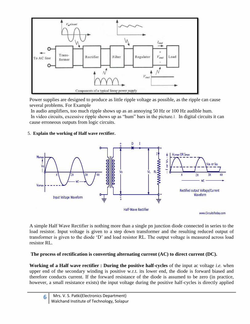
4. Explain power supply block diagram .
The purpose of a power supply is to take electrical energy in one form and convert it into another.,
supply from 230V, 50Hz AC mains is converted into smooth DC using AC-DC power supply. A power
supply can by broken down into a series of blocks, each of which performs a particular function. A
transformer first steps down high voltage AC to low voltage AC. A rectifier circuit is then used to
convert AC to DC. This DC, however, contains ripples, which can be smoothened by a filter circuit. A
regulated power supply maintains a constant DC output voltage through ‘feedback action’.
Main components of a regulated supply to convert 230V AC voltage to 5V DC are shown below.
6 Mrs. V. S. Patki(Electronics Department) Walchand Institute of Technology, Solapur
Power supplies are designed to produce as little ripple voltage as possible, as the ripple can cause
several problems. For Example
In audio amplifiers, too much ripple shows up as an annoying 50 Hz or 100 Hz audible hum.
In video circuits, excessive ripple shows up as “hum” bars in the picture. In digital circuits it can
cause erroneous outputs from logic circuits.
5. Explain the working of Half wave rectifier.
A simple Half Wave Rectifier is nothing more than a single pn junction diode connected in series to the
load resistor. Input voltage is given to a step down transformer and the resulting reduced output of
transformer is given to the diode ‘D’ and load resistor RL. The output voltage is measured across load
resistor RL.
The process of rectification is converting alternating current (AC) to direct current (DC).
Working of a Half wave rectifier : During the positive half-cycles of the input ac voltage i.e. when
upper end of the secondary winding is positive w.r.t. its lower end, the diode is forward biased and
therefore conducts current. If the forward resistance of the diode is assumed to be zero (in practice,
however, a small resistance exists) the input voltage during the positive half-cycles is directly applied
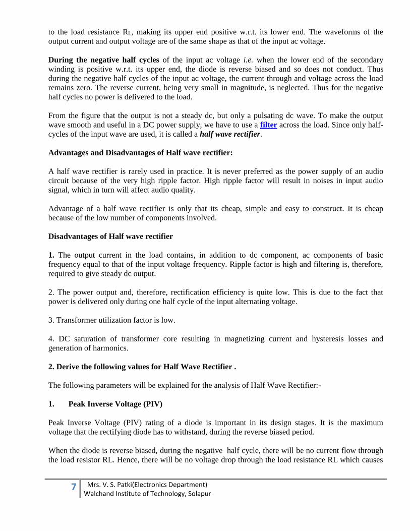
7 Mrs. V. S. Patki(Electronics Department) Walchand Institute of Technology, Solapur
to the load resistance RL, making its upper end positive w.r.t. its lower end. The waveforms of the
output current and output voltage are of the same shape as that of the input ac voltage.
During the negative half cycles of the input ac voltage i.e. when the lower end of the secondary
winding is positive w.r.t. its upper end, the diode is reverse biased and so does not conduct. Thus
during the negative half cycles of the input ac voltage, the current through and voltage across the load
remains zero. The reverse current, being very small in magnitude, is neglected. Thus for the negative
half cycles no power is delivered to the load.
From the figure that the output is not a steady dc, but only a pulsating dc wave. To make the output
wave smooth and useful in a DC power supply, we have to use a filter across the load. Since only half-
cycles of the input wave are used, it is called a half wave rectifier.
Advantages and Disadvantages of Half wave rectifier:
A half wave rectifier is rarely used in practice. It is never preferred as the power supply of an audio
circuit because of the very high ripple factor. High ripple factor will result in noises in input audio
signal, which in turn will affect audio quality.
Advantage of a half wave rectifier is only that its cheap, simple and easy to construct. It is cheap
because of the low number of components involved.
Disadvantages of Half wave rectifier
1. The output current in the load contains, in addition to dc component, ac components of basic
frequency equal to that of the input voltage frequency. Ripple factor is high and filtering is, therefore,
required to give steady dc output.
2. The power output and, therefore, rectification efficiency is quite low. This is due to the fact that
power is delivered only during one half cycle of the input alternating voltage.
3. Transformer utilization factor is low.
4. DC saturation of transformer core resulting in magnetizing current and hysteresis losses and
generation of harmonics.
2. Derive the following values for Half Wave Rectifier .
The following parameters will be explained for the analysis of Half Wave Rectifier:-
1. Peak Inverse Voltage (PIV)
Peak Inverse Voltage (PIV) rating of a diode is important in its design stages. It is the maximum
voltage that the rectifying diode has to withstand, during the reverse biased period.
When the diode is reverse biased, during the negative half cycle, there will be no current flow through
the load resistor RL. Hence, there will be no voltage drop through the load resistance RL which causes
8 Mrs. V. S. Patki(Electronics Department) Walchand Institute of Technology, Solapur
the entire input voltage to appear across the diode. Thus VSMAX, the peak secondary voltage, appears
across the diode. Therefore,
Peak Inverse Voltage (PIV) of half wave rectifier = VSMAX
2. Average and Peak Currents in the diode
By assuming that the voltage across the transformer secondary be sinusoidal of peak values VSMAX,
instantaneous value of the voltage given to the rectifier can be written as
Instantaneous value of voltage applied to Half Wave Rectifier Assuming that the diode has a
forward resistance of RF ohms and infinite reverse resistance value, the current flowing through
the output load resistance RL is
Current flowing through the diode IMAX = VSMAX / (RF + RL)
3. DC Output Current-- The dc output current is given as
Substituting the value of IMAX for the equation IMAX = VSMAX/(RF + RL), we have
Idc = VSMAX/ = VSMAX/ πRL if RL >> RF
4. DC Output Voltage
Vdc = Idc RL = VSMAX / π (RF + RL)X RL = VSMAX/{1+RF/RL } If RL >> RF, Vdc = VSMAX/π
5. Root Mean Square (RMS) Value of Current
9 Mrs. V. S. Patki(Electronics Department) Walchand Institute of Technology, Solapur
6. Root Mean Square (RMS) Value of Output Voltage
RMS value of voltage across the load is given as
VLrms = Irms RL = VSMAX RL /2(RF + RL) If RL >> RF, VLrms = VSMAX/2
7. Rectification Efficiency
Rectification efficiency is defined as the ratio between the output power to the ac input power.
Efficiency, Ƞ = DC power delivered to the load / AC input power from the transformer = Pdc/Pac
DC power delivered to the load, Pdc = I2dc RL = (Imax / π)2 RL
AC power input to the transformer, Pac = Power dissipated in diode junction + Power dissipated in load
resistance RL
= I2rms RF + I2
rms RL = {I2MAX/4}[ RF + RL]
So, Rectification Efficiency, Ƞ = Pdc/Pac = {4/π2}[ RL/ (RF + RL)] = 0.406 if RL >> RF,
The maximum efficiency that can be obtained by the half wave rectifier is 40.6%. This is obtained if RF
is neglected.
8. Ripple Factor
It is the ratio of the effective value of the ac components of voltage (or current) present in the output
from the rectifier to the dc component in output voltage (or current).
The effective value of the load current is given as
I2 =I2dc+I2
1+I22+I2
4 = I2dc +I2
ac
So, ripple factor, γ = Iac/ Idc = (I2 – I2dc)/ Idc = {( Irms/ Idc
2)-1} = (Kf2 – 1)
Where Kf is the form factor of the input voltage. For half wave rectifier, form factor is given as
Kf = Irms /Iavg = (Imax/2)/ (Imax/π) = π/2 = 1.57
So, ripple factor, γ = (1.572 – 1) = 1.21
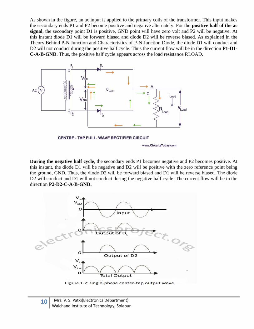
6. Explain cetre tap full wave rectifier.
In the case of centre-tap full wave rectifier, only two diodes are used, and are connected to the opposite
ends of a centre-tapped secondary transformer as shown in the figure below. The centre-tap is usually
considered as the ground point or the zero voltage reference point.
10 Mrs. V. S. Patki(Electronics Department) Walchand Institute of Technology, Solapur
As shown in the figure, an ac input is applied to the primary coils of the transformer. This input makes
the secondary ends P1 and P2 become positive and negative alternately. For the positive half of the ac
signal, the secondary point D1 is positive, GND point will have zero volt and P2 will be negative. At
this instant diode D1 will be forward biased and diode D2 will be reverse biased. As explained in the
Theory Behind P-N Junction and Characteristics of P-N Junction Diode, the diode D1 will conduct and
D2 will not conduct during the positive half cycle. Thus the current flow will be in the direction P1-D1-
C-A-B-GND. Thus, the positive half cycle appears across the load resistance RLOAD.
During the negative half cycle, the secondary ends P1 becomes negative and P2 becomes positive. At
this instant, the diode D1 will be negative and D2 will be positive with the zero reference point being
the ground, GND. Thus, the diode D2 will be forward biased and D1 will be reverse biased. The diode
D2 will conduct and D1 will not conduct during the negative half cycle. The current flow will be in the
direction P2-D2-C-A-B-GND.
11 Mrs. V. S. Patki(Electronics Department) Walchand Institute of Technology, Solapur
When comparing the current flow in the positive and negative half cycles, we can conclude that the
direction of the current flow is the same (through load resistance RLOAD). When compared to the
Half-Wave Rectifier, both the half cycles are used to produce the corresponding output. The frequency
of the rectified output voltage is twice the input frequency. The output that is rectified, consists of a
dc component and a lot of ac components of minute amplitudes.
1. Peak Inverse Voltage (PIV) of Centre-Tap Full Wave Rectifier
PIV is the maximum possible voltage across a diode during its reverse biased period. Let us analyze the
PIV of the centre-tapped rectifier from the circuit diagram. During the first half or the positive half of th
input ac supply, the diode D1 is positive and thus conducts and provided no resistance at all. Thus, the
whole of voltage Vs developed in the upper-half of the ac supply is provided to the load resistance
RLOAD. Similar is the case of diode D2 for the lower half of the transformer secondary.
Therefore, PIV of D2 = Vm + Vm = 2Vm PIV of D1 = 2Vm
2. Output Current
3. DC Output Voltage
Vdc = Idc x RL = 2 Im RL / π
4. Root Mean Square (RMS) Value of Current
5. Root Mean Square (RMS) Value of Output Voltage
V rms = Vm / √2
6. Rectification Efficiency
AC power input to the transformer, Pac = Power dissipated in diode junction + Power dissipated
Rectification efficiency is defined as the ratio between the output power to the ac input power.
Efficiency, Ƞ = DC power delivered to the load / AC input power from the transformer = Pdc/Pac
DC power delivered to the load, Pdc = I2dc RL = ( 2 Imax / π)2 RL
in load resistance RL

12 Mrs. V. S. Patki(Electronics Department) Walchand Institute of Technology, Solapur
= I2rms RF + I2
rms RL = {I2MAX/2}[ RF + RL]
So, Rectification Efficiency, Ƞ = Pdc/Pac = {8/π2}[ RL/ (RF + RL)] = 0.812 if RL >> RF,
The maximum efficiency that can be obtained by the full wave rectifier is 81.2%. This is obtained if RF
is neglected.
7. Ripple Factor: Form factor of the rectified output voltage of a full wave rectifier is given as
So, ripple factor, γ = (1.112 – 1) = 0.482
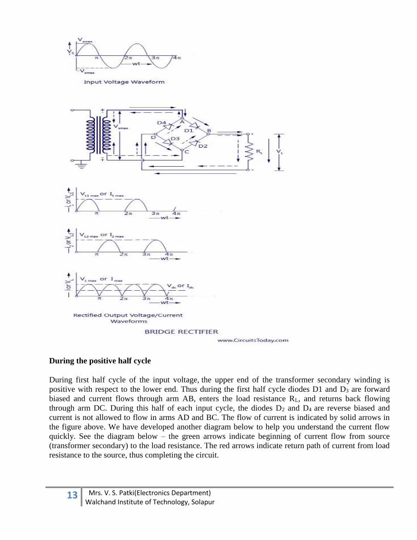
7. Explain Full wave bridge rectifier.
In the circuit diagram, 4 diodes are arranged in the form of a bridge. The transformer secondary is
connected to two diametrically opposite points of the bridge at points A & C. The load resistance RL is
connected to bridge through points B and D.
13 Mrs. V. S. Patki(Electronics Department) Walchand Institute of Technology, Solapur
During the positive half cycle
During first half cycle of the input voltage, the upper end of the transformer secondary winding is
positive with respect to the lower end. Thus during the first half cycle diodes D1 and D3 are forward
biased and current flows through arm AB, enters the load resistance RL, and returns back flowing
through arm DC. During this half of each input cycle, the diodes D2 and D4 are reverse biased and
current is not allowed to flow in arms AD and BC. The flow of current is indicated by solid arrows in
the figure above. We have developed another diagram below to help you understand the current flow
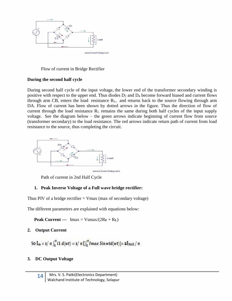
quickly. See the diagram below – the green arrows indicate beginning of current flow from source
(transformer secondary) to the load resistance. The red arrows indicate return path of current from load
resistance to the source, thus completing the circuit.
14 Mrs. V. S. Patki(Electronics Department) Walchand Institute of Technology, Solapur
Flow of current in Bridge Rectifier
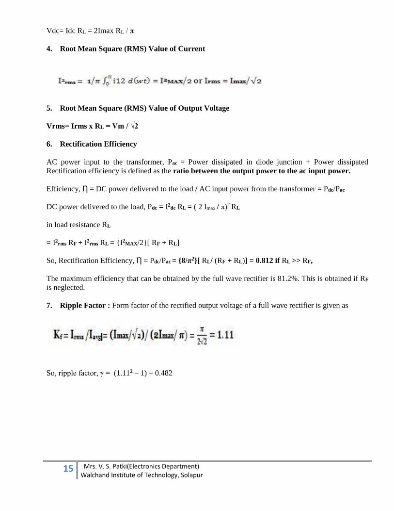
During the second half cycle
During second half cycle of the input voltage, the lower end of the transformer secondary winding is
positive with respect to the upper end. Thus diodes D2 and D4 become forward biased and current flows
through arm CB, enters the load resistance RL, and returns back to the source flowing through arm
DA. Flow of current has been shown by dotted arrows in the figure. Thus the direction of flow of
current through the load resistance RL remains the same during both half cycles of the input supply
voltage. See the diagram below – the green arrows indicate beginning of current flow from source
(transformer secondary) to the load resistance. The red arrows indicate return path of current from load
resistance to the source, thus completing the circuit.
Path of current in 2nd Half Cycle
1. Peak Inverse Voltage of a Full wave bridge rectifier:
Thus PIV of a bridge rectifier = Vmax (max of secondary voltage)
The different parameters are explained with equations below:
Peak Current --- Imax = Vsmax/(2RF + RL)
2. Output Current
3. DC Output Voltage
15 Mrs. V. S. Patki(Electronics Department) Walchand Institute of Technology, Solapur
Vdc= Idc RL = 2Imax RL / π
4. Root Mean Square (RMS) Value of Current
5. Root Mean Square (RMS) Value of Output Voltage
Vrms= Irms x RL = Vm / √2
6. Rectification Efficiency
AC power input to the transformer, Pac = Power dissipated in diode junction + Power dissipated
Rectification efficiency is defined as the ratio between the output power to the ac input power.
Efficiency, Ƞ = DC power delivered to the load / AC input power from the transformer = Pdc/Pac
DC power delivered to the load, Pdc = I2dc RL = ( 2 Imax / π)2 RL
in load resistance RL
= I2rms RF + I2
rms RL = {I2MAX/2}[ RF + RL]
So, Rectification Efficiency, Ƞ = Pdc/Pac = {8/π2}[ RL/ (RF + RL)] = 0.812 if RL >> RF,
The maximum efficiency that can be obtained by the full wave rectifier is 81.2%. This is obtained if RF
is neglected.
7. Ripple Factor : Form factor of the rectified output voltage of a full wave rectifier is given as
So, ripple factor, γ = (1.112 – 1) = 0.482
16 Mrs. V. S. Patki(Electronics Department) Walchand Institute of Technology, Solapur
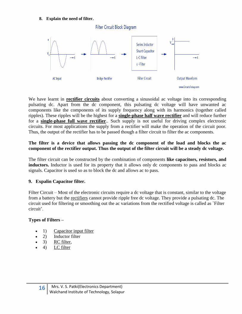
8. Explain the need of filter.
We have learnt in rectifier circuits about converting a sinusoidal ac voltage into its corresponding
pulsating dc. Apart from the dc component, this pulsating dc voltage will have unwanted ac
components like the components of its supply frequency along with its harmonics (together called
ripples). These ripples will be the highest for a single-phase half wave rectifier and will reduce further
for a single-phase full wave rectifier.. Such supply is not useful for driving complex electronic
circuits. For most applications the supply from a rectifier will make the operation of the circuit poor.
Thus, the output of the rectifier has to be passed though a filter circuit to filter the ac components.
The filter is a device that allows passing the dc component of the load and blocks the ac
component of the rectifier output. Thus the output of the filter circuit will be a steady dc voltage.
The filter circuit can be constructed by the combination of components like capacitors, resistors, and
inductors. Inductor is used for its property that it allows only dc components to pass and blocks ac
signals. Capacitor is used so as to block the dc and allows ac to pass.
9. Expalin Capacitor filter.
Filter Circuit – Most of the electronic circuits require a dc voltage that is constant, similar to the voltage
from a battery but the rectifiers cannot provide ripple free dc voltage. They provide a pulsating dc. The
circuit used for filtering or smoothing out the ac variations from the rectified voltage is called as `Filter
circuit’.
Types of Filters –
• 1) Capacitor input filter
• 2) Inductor filter
• 3) RC filter,
• 4) LC filter
17 Mrs. V. S. Patki(Electronics Department) Walchand Institute of Technology, Solapur
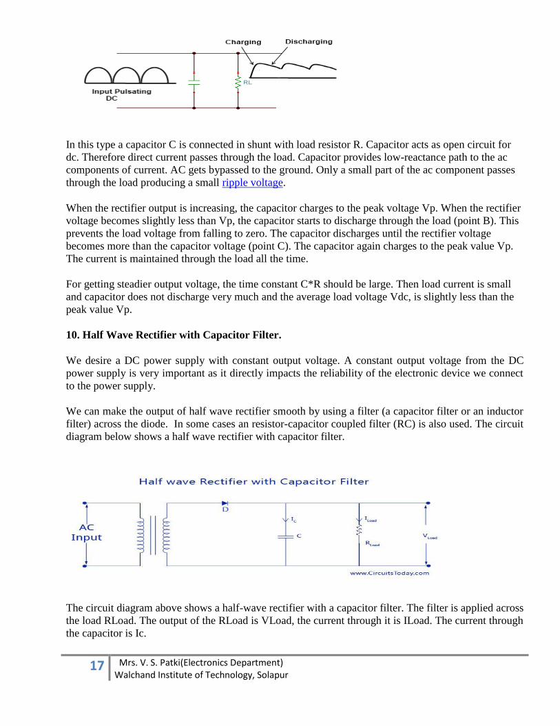
In this type a capacitor C is connected in shunt with load resistor R. Capacitor acts as open circuit for
dc. Therefore direct current passes through the load. Capacitor provides low-reactance path to the ac
components of current. AC gets bypassed to the ground. Only a small part of the ac component passes
through the load producing a small ripple voltage.
When the rectifier output is increasing, the capacitor charges to the peak voltage Vp. When the rectifier
voltage becomes slightly less than Vp, the capacitor starts to discharge through the load (point B). This
prevents the load voltage from falling to zero. The capacitor discharges until the rectifier voltage
becomes more than the capacitor voltage (point C). The capacitor again charges to the peak value Vp.
The current is maintained through the load all the time.
For getting steadier output voltage, the time constant C*R should be large. Then load current is small
and capacitor does not discharge very much and the average load voltage Vdc, is slightly less than the
peak value Vp.
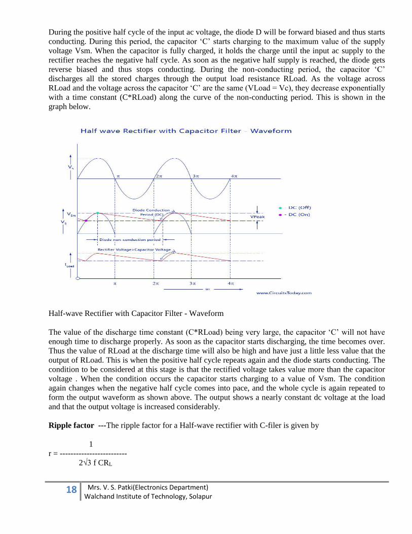
10. Half Wave Rectifier with Capacitor Filter.
We desire a DC power supply with constant output voltage. A constant output voltage from the DC
power supply is very important as it directly impacts the reliability of the electronic device we connect
to the power supply.
We can make the output of half wave rectifier smooth by using a filter (a capacitor filter or an inductor
filter) across the diode. In some cases an resistor-capacitor coupled filter (RC) is also used. The circuit
diagram below shows a half wave rectifier with capacitor filter.
The circuit diagram above shows a half-wave rectifier with a capacitor filter. The filter is applied across
the load RLoad. The output of the RLoad is VLoad, the current through it is ILoad. The current through
the capacitor is Ic.
18 Mrs. V. S. Patki(Electronics Department) Walchand Institute of Technology, Solapur
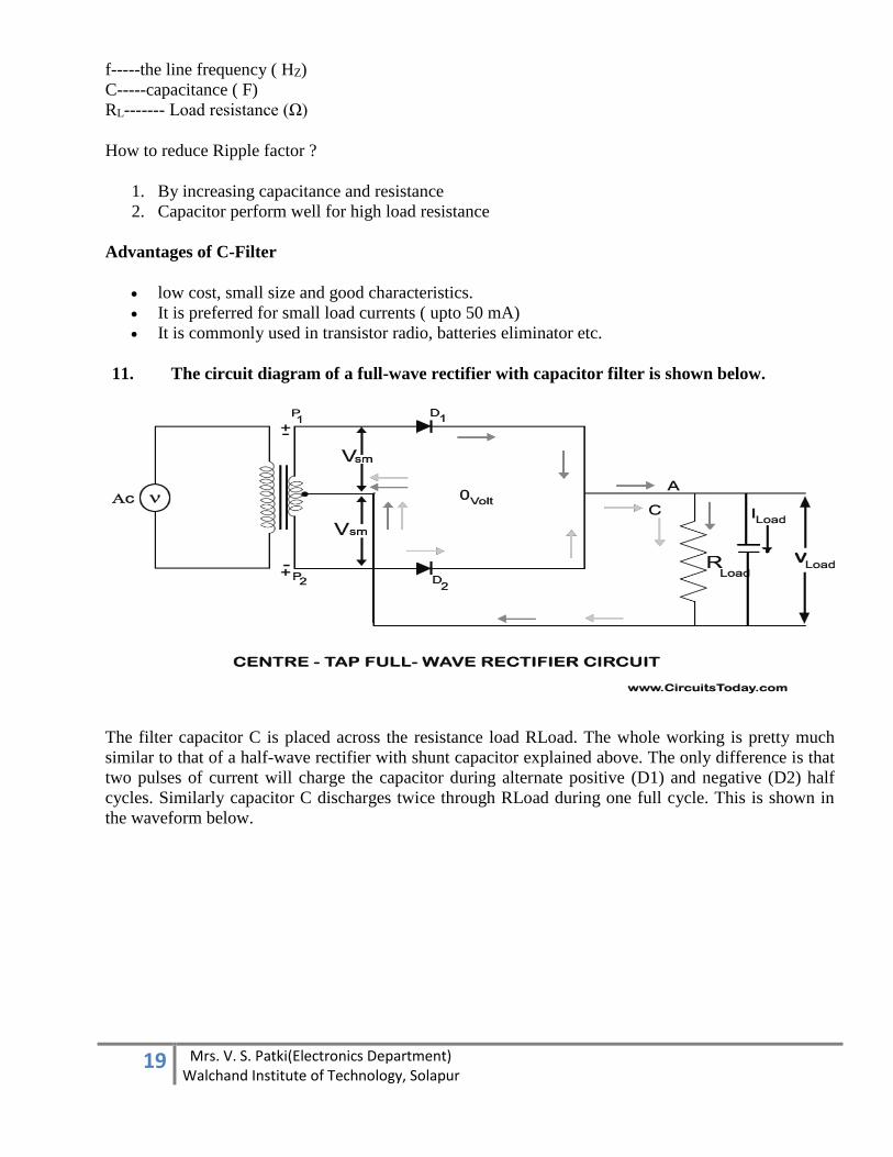
During the positive half cycle of the input ac voltage, the diode D will be forward biased and thus starts
conducting. During this period, the capacitor ‘C’ starts charging to the maximum value of the supply
voltage Vsm. When the capacitor is fully charged, it holds the charge until the input ac supply to the
rectifier reaches the negative half cycle. As soon as the negative half supply is reached, the diode gets
reverse biased and thus stops conducting. During the non-conducting period, the capacitor ‘C’
discharges all the stored charges through the output load resistance RLoad. As the voltage across
RLoad and the voltage across the capacitor ‘C’ are the same (VLoad = Vc), they decrease exponentially
with a time constant (C*RLoad) along the curve of the non-conducting period. This is shown in the
graph below.
Half-wave Rectifier with Capacitor Filter - Waveform
The value of the discharge time constant (C*RLoad) being very large, the capacitor ‘C’ will not have
enough time to discharge properly. As soon as the capacitor starts discharging, the time becomes over.
Thus the value of RLoad at the discharge time will also be high and have just a little less value that the
output of RLoad. This is when the positive half cycle repeats again and the diode starts conducting. The
condition to be considered at this stage is that the rectified voltage takes value more than the capacitor
voltage . When the condition occurs the capacitor starts charging to a value of Vsm. The condition
again changes when the negative half cycle comes into pace, and the whole cycle is again repeated to
form the output waveform as shown above. The output shows a nearly constant dc voltage at the load
and that the output voltage is increased considerably.
Ripple factor ---The ripple factor for a Half-wave rectifier with C-filer is given by
1
r = -------------------------
2√3 f CRL
19 Mrs. V. S. Patki(Electronics Department) Walchand Institute of Technology, Solapur
f-----the line frequency ( HZ)
C-----capacitance ( F)
RL------- Load resistance (Ω)
How to reduce Ripple factor ?
1. By increasing capacitance and resistance
2. Capacitor perform well for high load resistance
Advantages of C-Filter
• low cost, small size and good characteristics.
• It is preferred for small load currents ( upto 50 mA)
• It is commonly used in transistor radio, batteries eliminator etc.
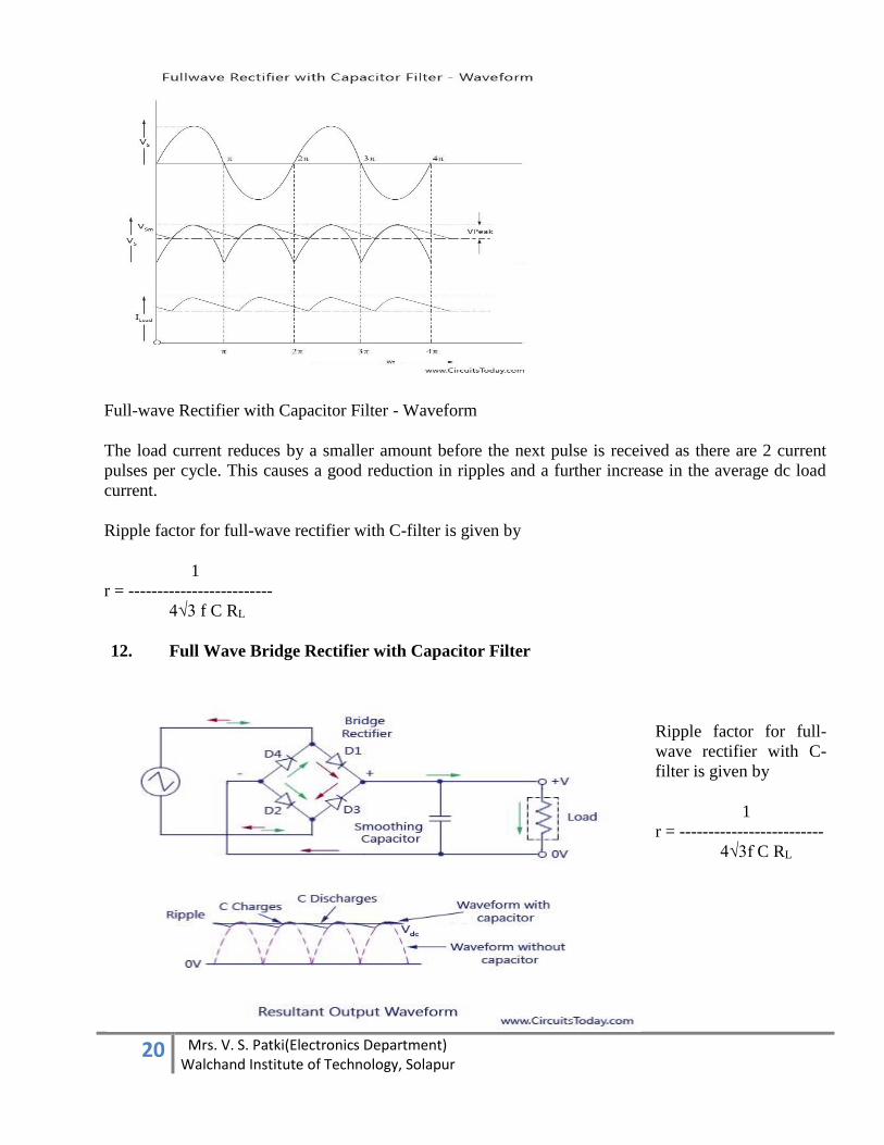
11. The circuit diagram of a full-wave rectifier with capacitor filter is shown below.
The filter capacitor C is placed across the resistance load RLoad. The whole working is pretty much
similar to that of a half-wave rectifier with shunt capacitor explained above. The only difference is that
two pulses of current will charge the capacitor during alternate positive (D1) and negative (D2) half
cycles. Similarly capacitor C discharges twice through RLoad during one full cycle. This is shown in
the waveform below.
20 Mrs. V. S. Patki(Electronics Department) Walchand Institute of Technology, Solapur
Full-wave Rectifier with Capacitor Filter - Waveform
The load current reduces by a smaller amount before the next pulse is received as there are 2 current
pulses per cycle. This causes a good reduction in ripples and a further increase in the average dc load
current.
Ripple factor for full-wave rectifier with C-filter is given by
1
r = -------------------------
4√3 f C RL
12. Full Wave Bridge Rectifier with Capacitor Filter
Ripple factor for full-
wave rectifier with C-
filter is given by
1
r = -------------------------
4√3f C RL