PL560/565-08 VCXO Family -...
12
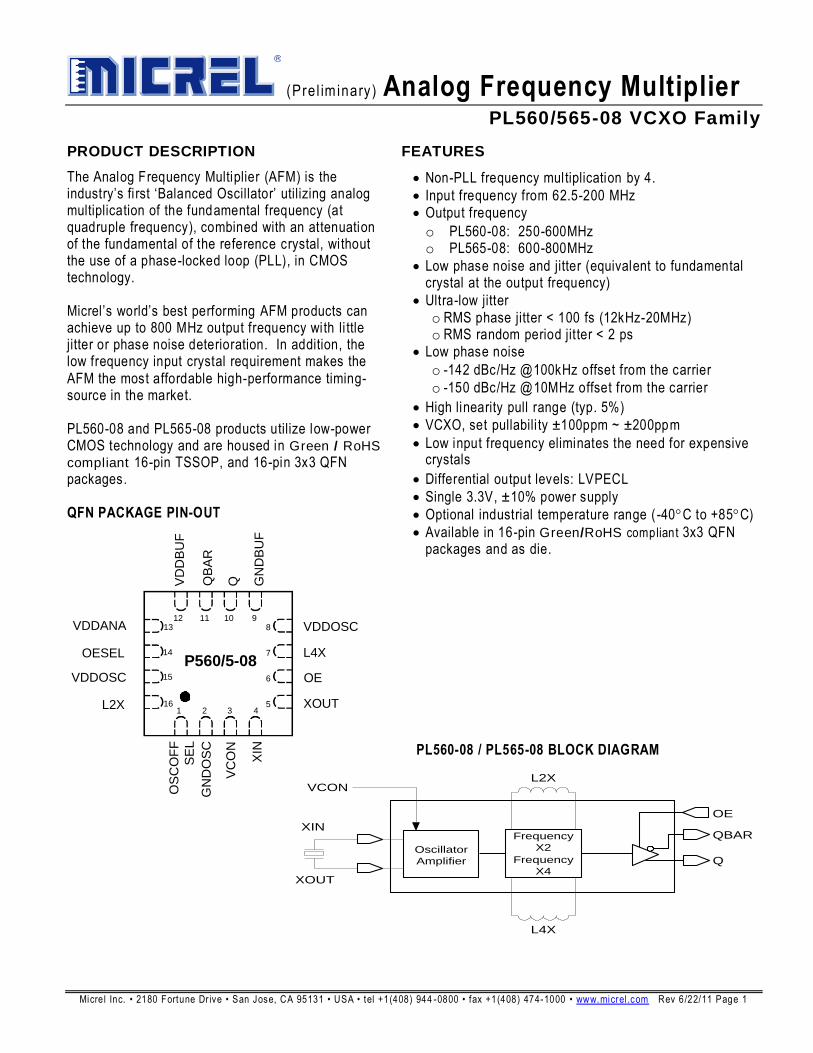
(Preliminary) Analog Frequency Multiplier PL560/565-08 VCXO Family Micrel Inc. • 2180 Fortune Drive • San Jose, CA 95131 • USA • tel +1(408) 944 - 0800 • fax +1(408) 474 - 1000 • www.micrel.com Rev 6/22/11 Page 1 PRODUCT DESCRIPTION The Analog Frequency Multiplier (AFM) is the industry’s first ‘Balanced Oscillator’ utilizing analog multiplication of the fundamental frequency (at quadruple frequency), combined with an attenuation of the fundamental of the reference crystal, without the use of a phase-locked loop (PLL), in CMOS technology. Micrel ’s world’s best performing AFM products can achieve up to 800 MHz output frequency with little jitter or phase noise deterioration. In addition, the low frequency input crystal requirement makes the AFM the most affordable high-performance timing- source in the market. PL560-08 and PL565-08 products utilize low-power CMOS technology and are housed in Green / RoHS compliant 16-pin TSSOP, and 16-pin 3x3 QFN packages. QFN PACKAGE PIN-OUT FEATURES Non-PLL frequency multiplication by 4. Input frequency from 62.5-200 MHz Output frequency o PL560-08: 250-600MHz o PL565-08: 600-800MHz Low phase noise and jitter (equivalent to fundamental crystal at the output frequency) Ultra-low jitter o RMS phase jitter < 100 fs (12kHz-20MHz) o RMS random period jitter < 2 ps Low phase noise o -142 dBc/Hz @100kHz offset from the carrier o -150 dBc/Hz @10MHz offset from the carrier High linearity pull range (typ. 5%) VCXO, set pullability ±100ppm ~ ±200ppm Low input frequency eliminates the need for expensive crystals Differential output levels: LVPECL Single 3.3V, ±10% power supply Optional industrial temperature range (-40 C to +85 C) Available in 16-pin Green / RoHS compliant 3x3 QFN packages and as die. PL560-08 / PL565-08 BLOCK DIAGRAM P560/5-08 VDDOSC OE XOUT L4X 1 2 3 4 12 11 10 9 13 14 15 16 8 7 6 5 VDDBUF Q GNDBUF QBAR OESEL VDDANA VDDOSC L2X GNDOSC OSCOFF SEL VCON XIN Oscillator Amplifier OE Q QBAR Frequency X2 XIN XOUT L2X VCON Frequency X4 L4X
Transcript of PL560/565-08 VCXO Family -...
(Pre l im inary ) Analog Frequency Multiplier PL560/565-08 VCXO Family
Micre l Inc. • 2180 Fortune Dr ive • San Jose, CA 95131 • USA • tel +1(408) 944 -0800 • fax +1(408) 474-1000 • www.micrel .com Rev 6/22/11 Page 1
PRODUCT DESCRIPTION
The Analog Frequency Multiplier (AFM) is the industry’s fi rst ‘Balanced Oscillator’ utilizing analog multiplication of the fundamental frequency (at quadruple frequency), combined with an attenuation of the fundamental of the reference crystal, without the use of a phase-locked loop (PLL), in CMOS technology. Micrel’s world’s best performing AFM products can achieve up to 800 MHz output frequency with li ttle jitter or phase noise deterioration. In addition, the low frequency input crystal requirement makes the AFM the most affordable high-performance timing-source in the market. PL560-08 and PL565-08 products utilize low-power CMOS technology and are housed in Green / RoHS
compliant 16-pin TSSOP, and 16-pin 3x3 QFN packages. QFN PACKAGE PIN-OUT
FEATURES
Non-PLL frequency multiplication by 4.
Input frequency from 62.5-200 MHz Output frequency
o PL560-08: 250-600MHz o PL565-08: 600-800MHz
Low phase noise and jitter (equivalent to fundamental crystal at the output frequency)
Ultra-low jitter o RMS phase jitter < 100 fs (12kHz-20MHz) o RMS random period jitter < 2 ps
Low phase noise
o -142 dBc/Hz @100kHz offset from the carrier
o -150 dBc/Hz @10MHz offset from the carrier
High linearity pull range (typ. 5%)
VCXO, set pullabili ty ±100ppm ~ ±200ppm
Low input frequency eliminates the need for expensive crystals
Differential output levels: LVPECL
Single 3.3V, ±10% power supply
Optional industrial temperature range ( -40C to +85C)
Available in 16-pin Green/RoHS compliant 3x3 QFN packages and as die.
PL560-08 / PL565-08 BLOCK DIAGRAM
P560/5-08
VDDOSC
OE
XOUT
L4X
1 2 3 4
12 11 10 913
14
15
16
8
7
6
5
VD
DB
UF
Q GN
DB
UF
QB
AR
OESEL
VDDANA
VDDOSC
L2X
GN
DO
SC
OS
CO
FF
SE
L
VC
ON
XIN
Oscillator
Amplifier
OE
Q
QBARFrequency
X2
XIN
XOUT
L2XVCON
Frequency
X4
L4X
(Pre l im inary ) Analog Frequency Multiplier PL560/565-08 VCXO Family
Micre l Inc. • 2180 Fortune Dr ive • San Jose, CA 95131 • USA • tel +1(408) 944 -0800 • fax +1(408) 474-1000 • www.micrel .com Rev 6/22/11 Page 2
DIE SPECIFICATIONS
SCRIBE LINE
SC
RIB
E L
INE
1 2 3 4 5 6
7
8
9
10
11
12
131415161718
19
20
21
22
Y
X0,0
1.3
85
mm
Die ID
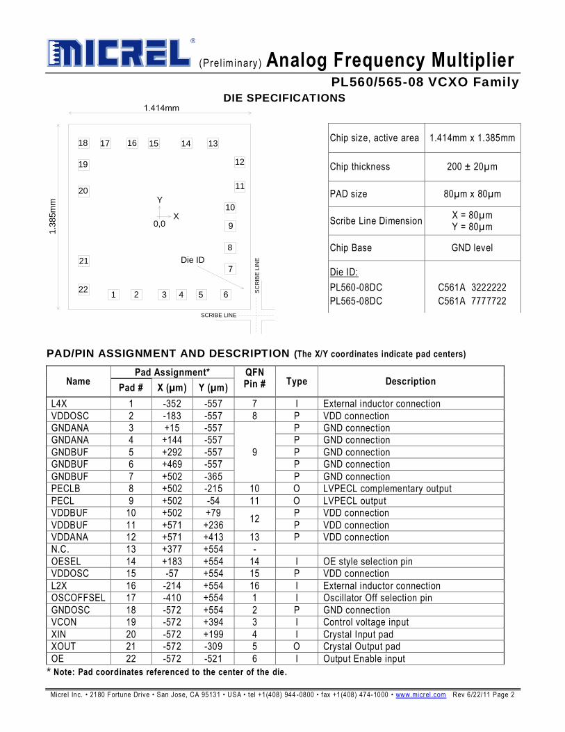
PAD/PIN ASSIGNMENT AND DESCRIPTION (The X/Y coordinates indicate pad centers)
Name Pad Assignment* QFN
Pin # Type Description Pad # X (µm) Y (µm)
L4X 1 -352 -557 7 I External inductor connection
VDDOSC 2 -183 -557 8 P VDD connection GNDANA 3 +15 -557
9
P GND connection GNDANA 4 +144 -557 P GND connection
GNDBUF 5 +292 -557 P GND connection GNDBUF 6 +469 -557 P GND connection
GNDBUF 7 +502 -365 P GND connection PECLB 8 +502 -215 10 O LVPECL complementary output
PECL 9 +502 -54 11 O LVPECL output VDDBUF 10 +502 +79
12 P VDD connection
VDDBUF 11 +571 +236 P VDD connection VDDANA 12 +571 +413 13 P VDD connection N.C. 13 +377 +554 -
OESEL 14 +183 +554 14 I OE style selection pin VDDOSC 15 -57 +554 15 P VDD connection
L2X 16 -214 +554 16 I External inductor connection OSCOFFSEL 17 -410 +554 1 I Oscillator Off selection pin
GNDOSC 18 -572 +554 2 P GND connection VCON 19 -572 +394 3 I Control voltage input
XIN 20 -572 +199 4 I Crystal Input pad XOUT 21 -572 -309 5 O Crystal Output pad
OE 22 -572 -521 6 I Output Enable input
* Note: Pad coordinates referenced to the center of the die.
Chip size, active area 1.414mm x 1.385mm
Chip thickness 200 ± 20µm
PAD size 80µm x 80µm
Scribe Line Dimension X = 80µm Y = 80µm
Chip Base GND level
Die ID:
PL560-08DC
PL565-08DC
C561A 3222222
C561A 7777722
(Pre l im inary ) Analog Frequency Multiplier PL560/565-08 VCXO Family
Micre l Inc. • 2180 Fortune Dr ive • San Jose, CA 95131 • USA • tel +1(408) 944 -0800 • fax +1(408) 474-1000 • www.micrel .com Rev 6/22/11 Page 3
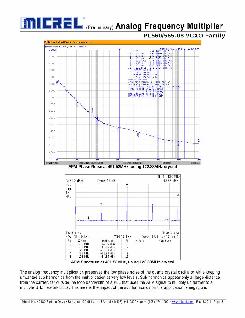
AFM Phase Noise at 491.52MHz, using 122.88MHz crystal
AFM Spectrum at 491.52MHz, using 122.88MHz crystal
The analog frequency multiplication preserves the low phase noise of the quartz crystal oscillator while keeping unwanted sub harmonics from the multiplication at very low levels. Sub harmonics appear only at large distance from the carrier, far outside the loop bandwidth of a PLL that uses the AFM signal to multiply up further to a multiple GHz network clock. This means the impact of the sub harmonics on the application is negligible.
(Pre l im inary ) Analog Frequency Multiplier PL560/565-08 VCXO Family
Micre l Inc. • 2180 Fortune Dr ive • San Jose, CA 95131 • USA • tel +1(408) 944 -0800 • fax +1(408) 474-1000 • www.micrel .com Rev 6/22/11 Page 4
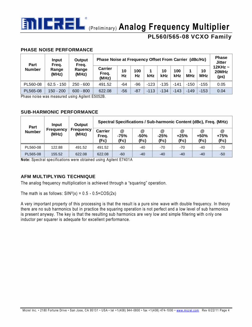
PHASE NOISE PERFORMANCE
Part Number
Input Freq.
Range (MHz)
Output Freq.
Range (MHz)
Phase Noise at Frequency Offset From Carrier (dBc/Hz) Phase Jitter
12KHz ~ 20MHz
(ps)
Carrier Freq. (MHz)
10 Hz
100 Hz
1 kHz
10 kHz
100 kHz
1 MHz
10 MHz
PL560-08 62.5 - 150 250 - 600 491.52 -64 -96 -123 -135 -141 -150 -155 0.05
PL565-08 150 - 200 600 - 800 622.08 -56 -87 -113 -134 -143 -149 -153 0.04
Phase noise was measured using Agilent E5052B.
SUB-HARMONIC PERFORMANCE
Part Number
Input Frequency
(MHz)
Output Frequency
(MHz)
Spectral Specifications / Sub-harmonic Content (dBc), Freq. (MHz)
Carrier Freq. (Fc)
@ -75% (Fc)
@ -50% (Fc)
@ -25% (Fc)
@ +25% (Fc)
@ +50% (Fc)
@ +75% (Fc)
PL560-08 122.88 491.52 491.52 -60 -40 -70 -70 -40 -70
PL565-08 155.52 622.08 622.08 -60 -40 -40 -40 -40 -50
Note: Spectral specifications were obtained using Agilent E7401A
AFM MULTIPLYING TECHNIQUE
The analog frequency multiplication is achieved through a “squaring” operation. The math is as follows: SIN²(x) = 0.5 - 0.5×COS(2x) A very important property of this processing is that the result is a pure sine wave with double frequency. In theory there are no sub harmonics but in practice the squaring operation is not perfect and a low level of sub harmonics is present anyway. The key is that the resulting sub harmonics are very low and simple filtering with o nly one inductor per squarer is adequate for excellent performance.
(Pre l im inary ) Analog Frequency Multiplier PL560/565-08 VCXO Family
Micre l Inc. • 2180 Fortune Dr ive • San Jose, CA 95131 • USA • tel +1(408) 944 -0800 • fax +1(408) 474-1000 • www.micrel .com Rev 6/22/11 Page 5
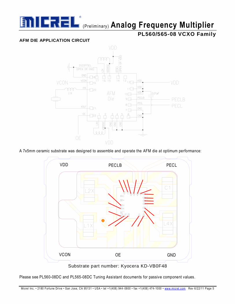
AFM DIE APPLICATION CIRCUIT
A 7x5mm ceramic substrate was designed to assemble and operate the AFM die at optimum performance:
Substrate part number: Kyocera KD-VB0F48
Please see PL560-08DC and PL565-08DC Tuning Assistant documents for passive component values.
VDD PECLB PECL
VCON OE GND
(Pre l im inary ) Analog Frequency Multiplier PL560/565-08 VCXO Family
Micre l Inc. • 2180 Fortune Dr ive • San Jose, CA 95131 • USA • tel +1(408) 944 -0800 • fax +1(408) 474-1000 • www.micrel .com Rev 6/22/11 Page 6
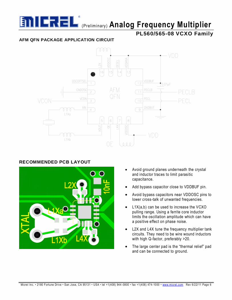
AFM QFN PACKAGE APPLICATION CIRCUIT
RECOMMENDED PCB LAYOUT
Avoid ground planes underneath the crystal and inductor traces to limit parasitic capacitance.
Add bypass capacitor close to VDDBUF pin.
Avoid bypass capacitors near VDDOSC pins to lower cross-talk of unwanted frequencies.
L1X(a,b) can be used to increase the VCXO pulling range. Using a ferri te core inductor limits the oscillation amplitude which can have a positive effect on phase noise.
L2X and L4X tune the frequency multiplier tank circuits. They need to be wire wound inductors with high Q-factor, preferably >20.
The large center pad is the “thermal relief” pad and can be connected to ground.
(Pre l im inary ) Analog Frequency Multiplier PL560/565-08 VCXO Family
Micre l Inc. • 2180 Fortune Dr ive • San Jose, CA 95131 • USA • tel +1(408) 944 -0800 • fax +1(408) 474-1000 • www.micrel .com Rev 6/22/11 Page 7
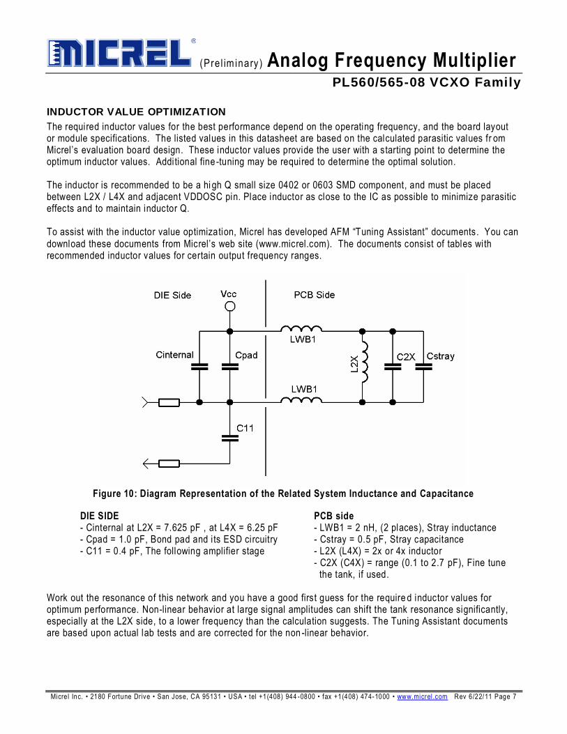
INDUCTOR VALUE OPTIMIZATION
The required inductor values for the best performance depend on the operating frequency, and the board layout or module specifications. The listed values in this datasheet are based on the calculated parasitic values fr om Micrel’s evaluation board design. These inductor values provide the user with a starting point to determine the optimum inductor values. Additional fine -tuning may be required to determine the optimal solution. The inductor is recommended to be a hi gh Q small size 0402 or 0603 SMD component, and must be placed between L2X / L4X and adjacent VDDOSC pin. Place inductor as close to the IC as possible to minimize parasitic effects and to maintain inductor Q. To assist with the inductor value optimization, Micrel has developed AFM “Tuning Assistant” documents. You can download these documents from Micrel’s web site (www.micrel.com). The documents consist of tables with recommended inductor values for certain output frequency ranges.
Figure 10: Diagram Representation of the Related System Inductance and Capacitance
DIE SIDE PCB side - Cinternal at L2X = 7.625 pF , at L4X = 6.25 pF - LWB1 = 2 nH, (2 places), Stray inductance - Cpad = 1.0 pF, Bond pad and i ts ESD circuitry - Cstray = 0.5 pF, Stray capacitance - C11 = 0.4 pF, The following amplifier stage - L2X (L4X) = 2x or 4x inductor
- C2X (C4X) = range (0.1 to 2.7 pF), Fine tune the tank, if used.
Work out the resonance of this network and you have a good first guess for the require d inductor values for optimum performance. Non-linear behavior at large signal amplitudes can shift the tank resonance significantly, especially at the L2X side, to a lower frequency than the calculation suggests. The Tuning Assistant documents are based upon actual lab tests and are corrected for the non -linear behavior.
(Pre l im inary ) Analog Frequency Multiplier PL560/565-08 VCXO Family
Micre l Inc. • 2180 Fortune Dr ive • San Jose, CA 95131 • USA • tel +1(408) 944 -0800 • fax +1(408) 474-1000 • www.micrel .com Rev 6/22/11 Page 8
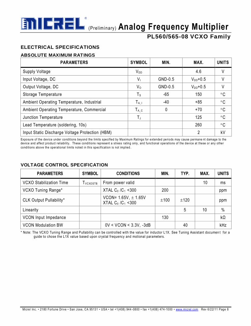
ELECTRICAL SPECIFICATIONS
ABSOLUTE MAXIMUM RATINGS
PARAMETERS SYMBOL MIN. MAX. UNITS
Supply Voltage VDD 4.6 V
Input Voltage, DC V I GND-0.5 VDD+0.5 V
Output Voltage, DC VO GND-0.5 VDD+0.5 V
Storage Temperature TS -65 150 C
Ambient Operating Temperature, Industrial TA_ I -40 +85 C
Ambient Operating Temperature, Commercial TA_ C 0 +70 C
Junction Temperature TJ 125 C
Lead Temperature (soldering, 10s) 260 C
Input Static Discharge Voltage Protection (HBM) 2 kV
Exposure of the device under condit ions beyond the limi ts speci fied by Maximum Ratings for extended periods may cause permane nt damage to the
device and af fect product rel iabi lity. These condit ions represent a s tress rat ing only , and functional operations of the device at these or any other
conditions above the operat ional limi ts noted in this specif icat ion is not impl ied .
VOLTAGE CONTROL SPECIFICATION
PARAMETERS SYMBOL CONDITIONS MIN. TYP. MAX. UNITS
VCXO Stabilization Time TVCXOSTB From power valid 10 ms
VCXO Tuning Range* XTAL C0 /C1 <300 200 ppm
CLK Output Pullability* VCON= 1.65V, 1.65V XTAL C0 /C1 <300
100 120 ppm
Linearity 5 10 %
VCON Input Impedance 130 kΩ
VCON Modulation BW 0V < VCON < 3.3V, -3dB 40 kHz
* Note: The VCXO Tuning Range and Pullability can be controlled with the value for inductor L1X. See Tuning Assistant documen t for a guide to chose the L1X value based upon crystal frequency and mot ional parameters.
(Pre l im inary ) Analog Frequency Multiplier PL560/565-08 VCXO Family
Micre l Inc. • 2180 Fortune Dr ive • San Jose, CA 95131 • USA • tel +1(408) 944 -0800 • fax +1(408) 474-1000 • www.micrel .com Rev 6/22/11 Page 9
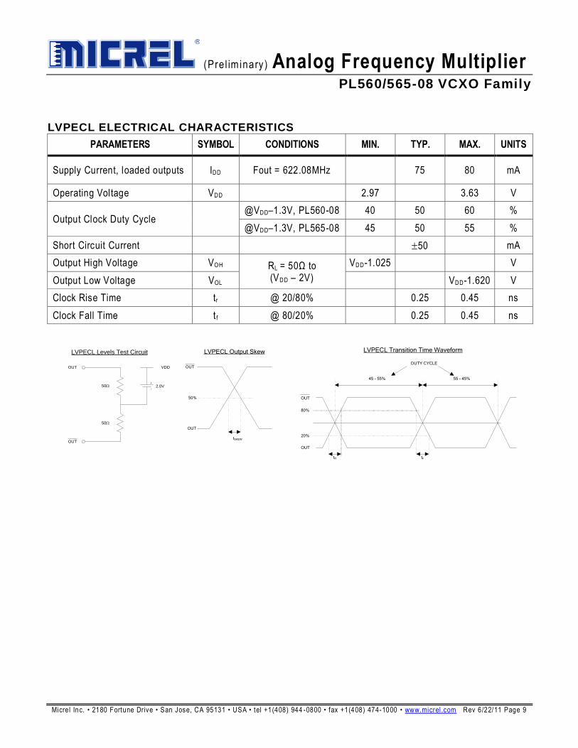
LVPECL ELECTRICAL CHARACTERISTICS
PARAMETERS SYMBOL CONDITIONS MIN. TYP. MAX. UNITS
Supply Current, loaded outputs IDD Fout = 622.08MHz 75 80 mA
Operating Voltage VDD 2.97 3.63 V
Output Clock Duty Cycle @VDD–1.3V, PL560-08 40 50 60 %
@VDD–1.3V, PL565-08 45 50 55 %
Short Circuit Current 50 mA
Output High Voltage VOH RL = 50Ω to (VDD – 2V)
VDD-1.025 V
Output Low Voltage VOL VDD-1.620 V
Clock Rise Time tr @ 20/80% 0.25 0.45 ns
Clock Fall Time t f @ 80/20% 0.25 0.45 ns
OUT
OUT
50?
50?
PECL Levels Test Circuit
LVPECL Transition Time Waveform
OUT
OUT
20%
80%
tR tF
VDD
DUTY CYCLE
45 - 55% 55 - 45%
50%
OUT
OUT
tSKEW
PECL Output Skew
2.0V
OUT
OUT
50
50
LVPECL Levels Test Circuit
PECL Transistion Time Waveform
OUT
OUT
50%
20%
80%
tR tF
VDD
DUTY CYCLE
45 - 55% 55 - 45%
50%
OUT
OUT
tSKEW
PECL Output Skew
2.0V
OUT
OUT
50?
50?
PECL Levels Test Circuit
PECL Transistion Time Waveform
OUT
OUT
50%
20%
80%
tR tF
VDD
DUTY CYCLE
45 - 55% 55 - 45%
50%
OUT
OUT
tSKEW
LVPECL Output Skew
2.0V
(Pre l im inary ) Analog Frequency Multiplier PL560/565-08 VCXO Family
Micre l Inc. • 2180 Fortune Dr ive • San Jose, CA 95131 • USA • tel +1(408) 944 -0800 • fax +1(408) 474-1000 • www.micrel .com Rev 6/22/11 Page 10
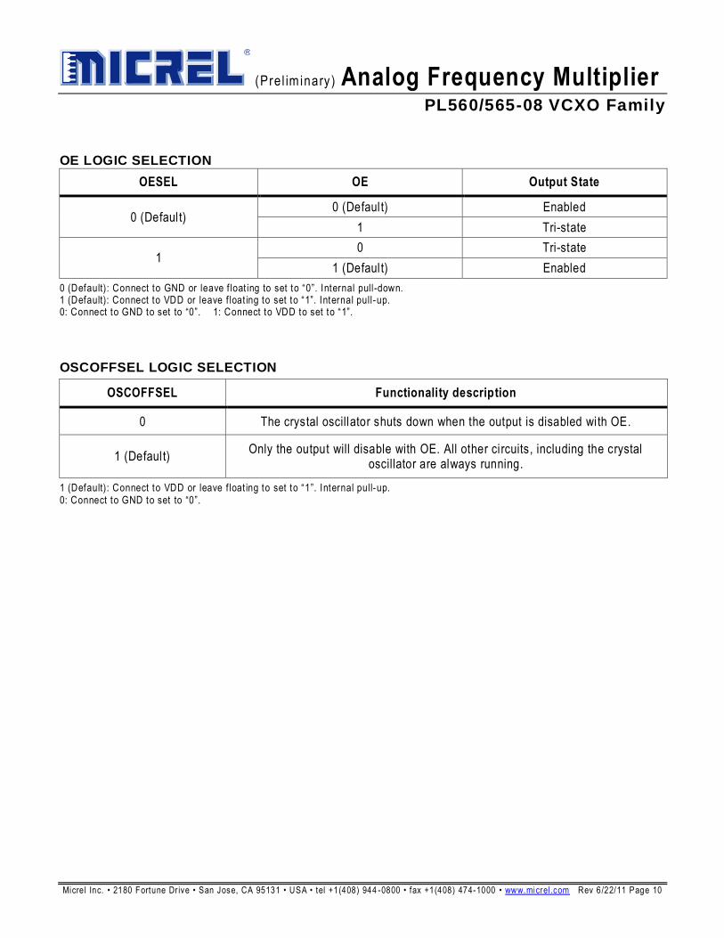
OE LOGIC SELECTION
OESEL OE Output State
0 (Default) 0 (Default) Enabled
1 Tri-state
1 0 Tri-state
1 (Default) Enabled
0 (Default): Connect to GND or leave f loat ing to set to “0”. Internal pull-down. 1 (Default): Connect to VDD or leave f loat ing to set to “1”. Internal pull-up. 0: Connect to GND to set to “0”. 1: Connect to VDD to set to “1”.
OSCOFFSEL LOGIC SELECTION
OSCOFFSEL Functionality description
0 The crystal oscillator shuts down when the output is disabled with OE.
1 (Default) Only the output will disable with OE. All other circuits, including the crystal
oscillator are always running.
1 (Default): Connect to VDD or leave f loat ing to set to “1”. Internal pull-up. 0: Connect to GND to set to “0”.
(Pre l im inary ) Analog Frequency Multiplier PL560/565-08 VCXO Family
Micre l Inc. • 2180 Fortune Dr ive • San Jose, CA 95131 • USA • tel +1(408) 944 -0800 • fax +1(408) 474-1000 • www.micrel .com Rev 6/22/11 Page 11
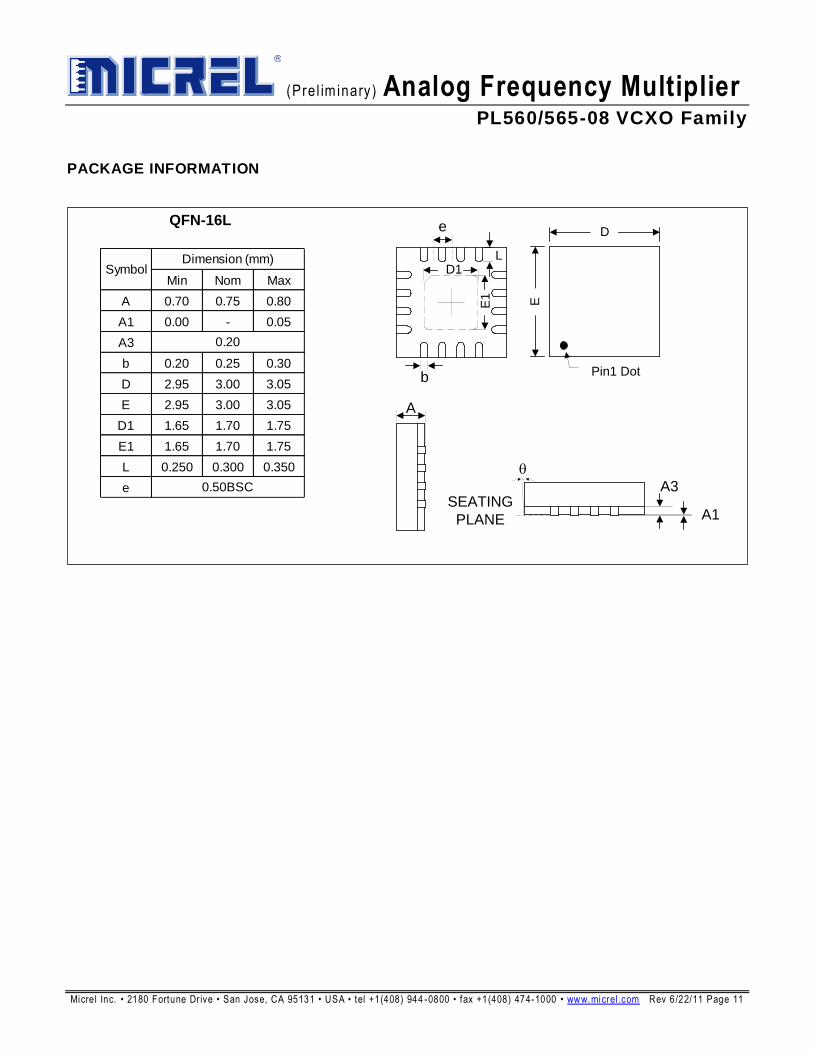
PACKAGE INFORMATION
QFN-16L
Pin1 Dot
DDD
DE
D
A
b
E1
D1
e
L
SEATING
PLANE A1
A3
Min Nom Max
A 0.70 0.75 0.80
A1 0.00 - 0.05
A3
b 0.20 0.25 0.30
D 2.95 3.00 3.05
E 2.95 3.00 3.05
D1 1.65 1.70 1.75
E1 1.65 1.70 1.75
L 0.250 0.300 0.350
e 0.50BSC
SymbolDimension (mm)
0.20
(Pre l im inary ) Analog Frequency Multiplier PL560/565-08 VCXO Family
Micre l Inc. • 2180 Fortune Dr ive • San Jose, CA 95131 • USA • tel +1(408) 944 -0800 • fax +1(408) 474-1000 • www.micrel .com Rev 6/22/11 Page 12
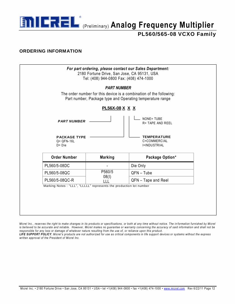
ORDERING INFORMATION
Micre l Inc. , reserves the right to make changes in i ts products or speci fications, or both at any t ime wi thout not ice. The in formation furnished by Micrel is believed to be accurate and re liab le. However, Micre l m akes no guarantee or warranty concerning the accuracy of said in format ion and shal l not be
responsible for any loss or damage of whatever nature resul ting from the use of, or re liance upon th is product. LIFE SUPPORT POLICY : Micre l’s products are not author ized for use as cr it ical components in li fe support devices or systems wi thout the express
wri tten approval of the President of Micrel Inc.
For part ordering, please contact our Sales Department: 2180 Fortune Drive, San Jose, CA 95131, USA
Tel: (408) 944-0800 Fax: (408) 474-1000
PART NUMBER
The order number for this device is a combination of the following: Part number, Package type and Operating temperature range
PL56X-08 X X X
Order Number Marking Package Option*
PL560/5-08DC - Die Only
PL560/5-08QC P560/5 08(I) LLL
QFN – Tube
PL560/5-08QC-R QFN – Tape and Reel
Marking Notes : “LLL”, “LLLLL” represents the production lo t number
PART NUMBER
TEMPERATURE C=COMMERCIAL
I=INDUSTRIAL
PACKAGE TYPE Q= QFN-16L D= Die
NONE= TUBE
R= TAPE AND REEL