All Digital VCXO Replacement for Gigabit Transceiver...
27
XAPP589 (v2.0) October 16, 2012 www.xilinx.com 1 © Copyright 2011–2012 Xilinx, Inc. Xilinx, the Xilinx logo, Artix, ISE, Kintex, Spartan, Virtex, Zynq, Vivado and other designated brands included herein are trademarks of Xilinx in the United States and other countries. All other trademarks are the property of their respective owners. Summary This application note delivers a system that is designed to replace external voltage controlled crystal oscillator (VCXO) circuits by utilizing functionality within each serial gigabit transceiver (GTX). A common design requirement is to frequency or phase lock a GTX output to an input source (known as loop, recovered, or slave timing). Traditionally, an external clock cleaning device or VCXO and PLL components are used to provide a high-quality clock reference for the GTX, since FPGA logic-based clocks are generally too noisy. While effective, external clock components carry a power and cost penalty that is additive as each individual clock channel is generated. When using many channels or in low-cost systems, the cost can be significant. Additionally, adding many external clock sources provides more opportunity for crosstalk and interference at the board level. The system described in this application note provides a method to effectively replace these external clock components using a combination of unique Xilinx GTX features in conjunction with a high-performance FPGA logic based digital PLL (DPLL). Each GTX has a phase interpolator (PI) circuit in the high-speed analog PLL output circuits that provides, on a individual GTX channel basis, the ability to phase and frequency modulate the transmit clock operating the GTX. Using a fully digital interface, the phase interpolator can be phase and frequency controlled from the FPGA logic resources under control of a high-resolution programmable DPLL. In conjunction with the FPGA logic DPLL, the phase interpolator provides the ability to phase or frequency modulate the GTX data output directly locking to an input reference pulse or clock while providing an built-in clock cleaning filter function. Unlike conventional solutions, high-quality system results because the clocking components are contained within the GTX. The reference design circuit provides a fully integrated DPLL and GTX phase interpolator system which can be instantiated for each transceiver channel used. The GTX can phase or frequency lock to an input reference signal. The DPLL enables generation of a synchronous GTX data output with run-time configurable parameters (e.g., gain, cutoff frequency, and clock divider values) to enable the user to set up the operation specifically for the end application. This particularly highlights the flexibility of the reference input signal and DPLL cleaning bandwidth. The reference design circuit can lock an individual GTX channel to up to ±160 ppm from the reference oscillator and programmatically provide jitter cleaning bandwidths in the range from 0.1 Hz to 1 KHz. The GTX transceiver block (in a Virtex-6 FPGA) operates at data rates of up to 3.125 Gb/s in the clock-locking mode. In the 7 series FPGAs, the GTX transceiver is capable of operating at up to 12.5 Gb/s. Typical applications for this circuit include video SD/HD/3G SDI, Sync E, IEEE1588, SDH, SONET, and OTN. System Applications A number of different applications need external VCXOs and PLLs or clock-cleaning components on a per transceiver transmitter basis. Some application examples include: • OTN muxponders for trunk to tributary slaving of outputs. Application Note: Virtex-6 and 7 Series FPGAs XAPP589 (v2.0) October 16, 2012 All Digital VCXO Replacement for Gigabit Transceiver Applications Authors: David Taylor, Matt Klein, and Vincent Vendramini
Transcript of All Digital VCXO Replacement for Gigabit Transceiver...

XAPP589 (v2.0) October 16, 2012 www.xilinx.com 1
© Copyright 2011–2012 Xilinx, Inc. Xilinx, the Xilinx logo, Artix, ISE, Kintex, Spartan, Virtex, Zynq, Vivado and other designated brands included herein are trademarks of Xilinx in the United States and other countries. All other trademarks are the property of their respective owners.
Summary This application note delivers a system that is designed to replace external voltage controlled crystal oscillator (VCXO) circuits by utilizing functionality within each serial gigabit transceiver (GTX).
A common design requirement is to frequency or phase lock a GTX output to an input source (known as loop, recovered, or slave timing). Traditionally, an external clock cleaning device or VCXO and PLL components are used to provide a high-quality clock reference for the GTX, since FPGA logic-based clocks are generally too noisy. While effective, external clock components carry a power and cost penalty that is additive as each individual clock channel is generated. When using many channels or in low-cost systems, the cost can be significant. Additionally, adding many external clock sources provides more opportunity for crosstalk and interference at the board level.
The system described in this application note provides a method to effectively replace these external clock components using a combination of unique Xilinx GTX features in conjunction with a high-performance FPGA logic based digital PLL (DPLL). Each GTX has a phase interpolator (PI) circuit in the high-speed analog PLL output circuits that provides, on a individual GTX channel basis, the ability to phase and frequency modulate the transmit clock operating the GTX. Using a fully digital interface, the phase interpolator can be phase and frequency controlled from the FPGA logic resources under control of a high-resolution programmable DPLL. In conjunction with the FPGA logic DPLL, the phase interpolator provides the ability to phase or frequency modulate the GTX data output directly locking to an input reference pulse or clock while providing an built-in clock cleaning filter function. Unlike conventional solutions, high-quality system results because the clocking components are contained within the GTX.
The reference design circuit provides a fully integrated DPLL and GTX phase interpolator system which can be instantiated for each transceiver channel used. The GTX can phase or frequency lock to an input reference signal. The DPLL enables generation of a synchronous GTX data output with run-time configurable parameters (e.g., gain, cutoff frequency, and clock divider values) to enable the user to set up the operation specifically for the end application. This particularly highlights the flexibility of the reference input signal and DPLL cleaning bandwidth.
The reference design circuit can lock an individual GTX channel to up to ±160 ppm from the reference oscillator and programmatically provide jitter cleaning bandwidths in the range from 0.1 Hz to 1 KHz. The GTX transceiver block (in a Virtex-6 FPGA) operates at data rates of up to 3.125 Gb/s in the clock-locking mode. In the 7 series FPGAs, the GTX transceiver is capable of operating at up to 12.5 Gb/s. Typical applications for this circuit include video SD/HD/3G SDI, Sync E, IEEE1588, SDH, SONET, and OTN.
System Applications
A number of different applications need external VCXOs and PLLs or clock-cleaning components on a per transceiver transmitter basis.
Some application examples include:
• OTN muxponders for trunk to tributary slaving of outputs.
Application Note: Virtex-6 and 7 Series FPGAs
XAPP589 (v2.0) October 16, 2012
All Digital VCXO Replacement for Gigabit Transceiver ApplicationsAuthors: David Taylor, Matt Klein, and Vincent Vendramini

System Applications
XAPP589 (v2.0) October 16, 2012 www.xilinx.com 2
• Broadcast equipment including switchers and routers using SD, HD, and 3G SDI video outputs.
• Synchronous Ethernet.
• Recovered media clock generation (per IEEE specification 1588).
External components used to do this task are a high-impact expense for several reasons:
• Significant BOM cost, an estimated $10 to $15 per additional VCXO/PLL or clock cleaner.
• Significant power consumption (300 mW to 500 mW) per additional VCXO/PLL or clock cleaner.
• Board space and PCB complexity, both due to additional board area required and careful noise-reduction design layout requirements.
Figure 1 shows a general use case where inputs are received through any one of a number of types of links carrying data. There could be one input link per output link or a group of input links that data is striped across, which are de-multiplexed to form output links. While each input link can share one reference clock, the challenge is that each output link needs its own VCXO/PLL or clock cleaning system to provide a clean reference to the transceiver to serialize outgoing data and produce the expected low-jitter output signal.
X-Ref Target - Figure 1
Figure 1: Typical Design with Multiple VCXOs (One per Unique Output Rate)
X589_01_041212
Inputs
Output #1
Output #2
Output #3
Output #4
Output #5
Output #N
Control/CLK
New CLK
Data
CTRL or CLK
Clean Clock
VCXO/PLL orClock Cleaner
SerDes
Dem
ultip
lexe
r, S
witc
her,
Rou
ter,
Cha
nnel
izer
SerDes
SerDes
SerDes
SerDes
SerDes
~$15 per VCXO
Inputs can share one XTAL, but each unique output needs a VCXO
System Applications
XAPP589 (v2.0) October 16, 2012 www.xilinx.com 3
By using GTX transceivers the need for external VCXO/PLLs and clock cleaners can be eliminated. The basics of the reference design method are:
• Each Virtex-6 FPGA and 7 series FPGAs GTX transceiver has a transmit clock phase interpolator (TX PI) for the transmit serial/deserializer bit clock.
• Each phase interpolator in each transmit serial/deserializer can be independently, dynamically, and continuously changed in phase and hence, shifted in frequency.
There are a number of benefits to this implementation:
• Significant BOM cost reduction, an estimated $15 to $20 per additional VCXO/PLL.
• Significant power consumption savings (300 mW to 500 mW) per VCXO/PLL.
• Reduced board space and PCB complexity.
• Ability to have four unique differentiated transmission rates within a GTX Quad.
An example block diagram of this new method is shown in Figure 2. The output VCXOs/PLLs or clock cleaners are brought into the FPGA using the GTX Quad’s phase-shifting functionality.
X-Ref Target - Figure 2
Figure 2: Phase-Shifting Solution Block Diagram
X589_02_041212
Inputs
Output #1
Output #2
Output #3
Output #4
Output #5
Output #N
DATA
Control
New CLKFixedREFCLK(s)
SerDes
Digital PLL
SerDes
DPLL
SerDes
DPLL
SerDes
DPLL
SerDes
DPLL
SerDes
DPLL
Dem
ulitp
lexe
r, S
witc
her,
Rou
ter,
Cha
nnel
izer
Output VCXOs Removed

System Applications
XAPP589 (v2.0) October 16, 2012 www.xilinx.com 4
Solution Examples
This section describes solutions for broadcast switcher or router applications and OTN trunk to tributary demultiplexer applications. Normally, an external VCXO/PLL or clock cleaner is required for each unique output transmit serial/deserializer channel. This is very expensive because each parts per million (PPM) channel variation requires an additional circuit, even if the output base rate is the same (e.g., 1.485 Gb/s + 50 ppm and 1.485 Gb/s – 20 ppm).
Example 1: Broadcast Switcher or Router
In this example (Figure 3), a broadcast switcher or router is receiving SD/HD/3G streams from different cameras or unrelated sources. The video is processed inside of an FPGA, but the outputs of FPGA must be exactly locked to some of the input channels. Individual HD-SDI and 3G-SDI inputs, for instance, while nominally running at 1.485 Gb/s and 2.97 Gb/s might not be locked to each other. The inputs could be locked to their original sources, which could vary from the nominal frequency by up to 150 ppm. Normally, when individual outputs of the FPGA are meant to be locked to these PPM varied inputs, the design includes an external VCXO/PLL or clock cleaner for each PPM varied output. By using the FPGA’s TX PI, the complex and expensive components are instead designed into the transmit serial/deserializer functionality.
X-Ref Target - Figure 3
Figure 3: Broadcast Switcher or Router without External VCXOs/PLLs or Clock Cleaners on the Outputs
X589_03_041212
SD/HD/3G #1
SD/HD/3G #1
SD/HD/3G #2
SD/HD/3G #3
SD/HD/3G #4
SD/HD/3G #N
REFCLK(1-2 Fixed XOs)
TX PI +SerDes
Phase Det.LPF, FRQCTRL
Digital PLL
TX PI CTRL
TX PI CTRL
TX PI CTRL
TX PI CTRL
TX PI CTRL
Digital PLL
Digital PLL
Digital PLL
Digital PLL
Rate Generator
FIFO
Logic Resources TX SerDesRX SerDes
SD/HD/3G #2
TX PI +SerDes
Phase Det.LPF, FRQCTRL
Rate Generator
FIFO
SD/HD/3G #3
TX PI +SerDes
Phase Det.LPF, FRQCTRL
Rate Generator
FIFO
SD/HD/3G #4
TX PI +SerDes
Phase Det.LPF, FRQCTRL
Rate Generator
FIFO
SD/HD/3G #N
TX PI +SerDes
Phase Det.LPF, FRQCTRL
Rate Generator
FIFO
RX SerDes
RX SerDes
RX SerDes
RX SerDes
RX SerDes
Rou
ting
and
Sw
itchi
ng F
unct
ion
System Applications
XAPP589 (v2.0) October 16, 2012 www.xilinx.com 5
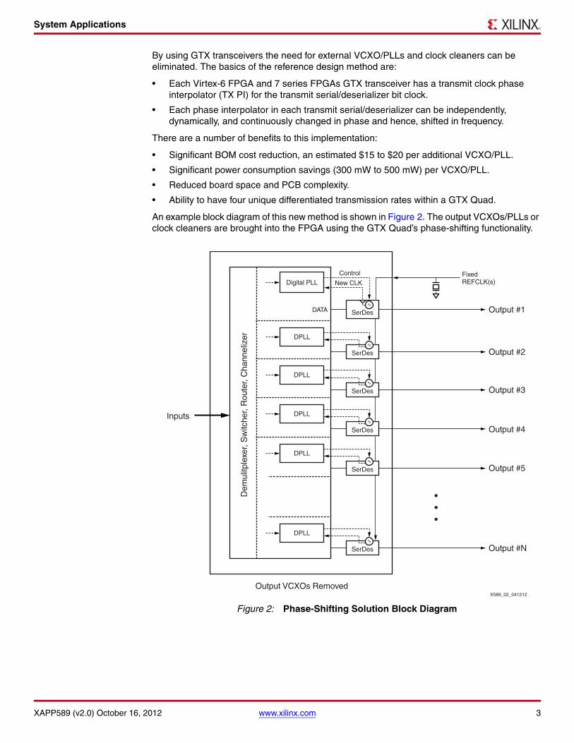
Example 2: OTN Muxponder
In this example (Figure 4), within an OTN trunk there are multiple streams of data. Each stream within the trunk has a unique rate. In a number of cases, an FPGA or other device receiving the trunk will demultiplex it into its component streams. Each source stream, even at approximately the same rate, has an oscillator or clock system that originally sourced the stream in the trunk. The timing of the recovered stream must be preserved on a stream by stream basis. For example, when there are multiple synchronous Ethernet streams that are each nominally at 1.25 Gb/s, but not from the same source, each stream (even if it is the same type) can vary by a few PPM. The recovered outputs must each be exactly locked to their original source, which requires a phase detector, low-pass filter, VCXO, and PLL external to the FPGA per unique output channel. The Xilinx FPGA’s TX PI in the transmit serial/deserializer can take fixed nominal oscillator rates as REFCLKs and effectively slave them within the transmit serial/deserializer to the unique recovered rate with low jitter and without the need for external VCXOs/PLLs or clock cleaners.
In these examples, and for many other cases, the unique Xilinx transmit clock phase interpolator functionality built into the transmit serial/deserializer and the FPGA-based phase detector, digital PLL, low-pass filter, and controlled transmit serial/deserializer phase interpolator replace expensive external VCXO/PLLs or clock cleaners.
X-Ref Target - Figure 4
Figure 4: OTN Trunk to Tributary Demultiplexor and Delivery without External VCXOs/PLLs or Clock Cleaners
X589_04_041212
REFCLK(Fixed XOs)
TX PI +SerDes
Phase Det.LPF, FRQCTRL
Digital PLL
TX PI CTRL
TX PI CTRL
TX PI CTRL
TX PI CTRL
TX PI CTRL
Digital PLL
Digital PLL
Digital PLL
Digital PLL
Rate Generator
FIFO
Logic Resources TX SerDesRX SerDes
10G/40G/100GTrunk with
Multiple Linksand Streams
Stream 1
Stream 2
Stream 3
Stream 4
Stream N
TX PI +SerDes
Phase Det.LPF, FRQCTRL
Rate Generator
FIFO
TX PI +SerDes
Phase Det.LPF, FRQCTRL
Rate Generator
FIFO
TX PI +SerDes
Phase Det.LPF, FRQCTRL
Rate Generator
FIFO
TX PI +SerDes
Phase Det.LPF, FRQCTRL
Rate Generator
FIFO
RX SerDes
RX SerDes Dem
ultip
lexe
r

VCXO Replacement Theory
XAPP589 (v2.0) October 16, 2012 www.xilinx.com 6
VCXO Replacement Theory
Virtex-6 FPGAs contain a key functional block in the GTX transceiver transmitter that enables functional replacement of a VCXO. This block, a phase interpolator, produces an output clock with a fine phase shift relative to an input clock. The fine phase shift is produced in response to a control word. The control word allows selection of a phase between 0° and 360°.
To create the equivalent of a VCXO with only a fixed frequency source, a phase is selected by the phase interpolator and the selected phase selection value is continuously updated with a linearly increasing or decreasing phase. This is equivalent to a positive or negative frequency shift proportional to the rate of change of the controlling phase. See Equation 1 through Equation 5.
Equation 1
Equation 2
Equation 3
Equation 4
Equation 5
From these equations, the output frequency is shifted by the rate of change of the control phase ΦCONTROL with respect to time.
Figure 5 shows a functional block diagram of the phase interpolator, which includes the inputs and outputs used in conjunction with the high-speed serial clock input from the SerDes transmit PLL and other circuits that participate in the complete solution. This block first produces a number of primary phases from the n-phase generation block. This block generates x phases separated by 360°/x. In the case of the transmit serial clock phase interpolator, there are eight primary phases (0°, 45°, 90°, 135°, 180°, 225°, 270°, and 315°). The phase-select block in Figure 5 selects two adjacent phases based on the control logic.
The phase interpolation function is performed by the phase mixer, which functionally combines k parts of Φ1 and (1 – k) parts of Φ2 (resulting in an interpolated phase output of Φ1k + Φ2(1 – k)), where k is a fraction between 0 and 1.
fdΦIN t( )
dt--------------------=
ΦIN t( ) f INdt fINt= =
ΦOUT t( ) ΦIN t( ) ΦCONTROL t( )+=
DifferentiatingdΦOUT t( )
dt--------------------------
dΦIN t( )dt
--------------------dΦCONTROL t( )
dt-----------------------------------------+=
fOUT
dΦOUT t( )dt
--------------------------, fOUT fINdΦCONTROL t( )
dt-----------------------------------------+==

VCXO Replacement Theory
XAPP589 (v2.0) October 16, 2012 www.xilinx.com 7
Figure 6 shows two primary phases (Φ1 and Φ2) selected from the n-phase generator that are interpolated by the phase mixer. The output is a clock with a phase that is in between Φ1and Φ2 with a resolution determined by the number of fractional steps allowed. For Virtex-6 FPGAs, the number of fractional steps is 15.
The primary phase generation and interpolated phase creation are all performed in a clean analog domain. The final result is a high-speed clock that can be any one of 120 phases of the high-speed transmit serial/deserializer clock and is used for serialization of the parallel transmit serial/deserializer data in the Virtex-6 FPGAs transmit serial/deserializer. This produces a very low jitter clock with very fine phase resolution.
A phase interpolator operates on the line rate and is present in each of the Virtex-6 FPGA GTX transceivers and all 7 series transceivers. It takes in an input clock and produces an output with a fine phase shift. The phase interpolator in the Virtex-6 FPGA GTX transceiver’s transmitter has a phase control port that can be accessed at a rate of up to approximately 30 MHz and a phase control resolution of approximately 1/120th of a unit interval (UI) of the transmitter’s serial line rate.
X-Ref Target - Figure 5
Figure 5: Functional Block Diagram of a SerDes Transmit PLL Feeding a Phase Interpolator
High SpeedSerDesClock
TransmitSerDes
PLLREFCLK
n-PhaseGeneration
xk
1–k
Dynamic Phase Control xapp589_05_042912
Phase Select
Control Logic
Where: φ2 – φ1 = 360°/x
Phase Mixer
Phase Interpolator
1
2
X-Ref Target - Figure 6
Figure 6: Phase Mixer Producing an Interpolated Phase from Coarse Phases
High SpeedSerDes Clock
Phase Mixer1
2
OUT
1 12
xapp589_06_042912
k
1–k

PICXO Operation
XAPP589 (v2.0) October 16, 2012 www.xilinx.com 8
Phase Resolution and Frequency Shift Example
Both phase resolution and frequency shift achieved by continuously updating the selected phase is outlined in this example:
• Transmitter serial/deserializer rate = 3.125 Gb/s
• Transmitter serial/deserializer clock period = 320 ps
• Phase interpolator step = 320/120 ps = 2.66 ps
• Update rate = 31.25 MHz
PICXO Operation
Instead of using an external VCXO, as described in VCXO Replacement Theory with its challenges, a complete digital PLL and clock cleaner can be created using the phase interpolator in the transmit serial/deserializer as a phase interpolator controlled crystal or Xtal oscillator (PICXO). The PICXO macro operation is shown in the functional block diagram of Figure 7.
The dynamic reconfiguration port (DRP) arbiter/FIFO and control blocks manage the clock and DRP data interfaces between the GTX transceiver, the PICXO DPLL, and the User DRP.
A typical use model for a DRP operation is that the user’s application can, if required, program GTX transceiver DRP parameters prior to operation. Subsequently, the PICXO is reset and locked to the reference clock/pulse started (see Physical Interface).
The phase in the GTX transceiver is under direct DRP control from the PICXO circuit consisting of phase accumulator, sigma delta modulator and loop filter, and phase detector components.
The phase accumulator tracks the current phase of the phase interpolator and increments or decrements the phase based on input from the sigma-delta modulator block. Incrementing or decrementing phases directly results in a negative or positive frequency offset.
The required fine frequency control is achieved by the sigma-delta modulation block driven by a second order DPLL consisting of filter and phase detector with user configurable loop parameters and comparison frequencies for maximum flexibility.
X-Ref Target - Figure 7
Figure 7: PICXO Macro Functional Block Diagram
Referenceclock/pulse
DRPData
CE
Error Volt
CE
CEDSP
CEPI
CE
UserDRP
1
CE
Sign
DO
DO
ADD_SUB
DI
DRPDEN
DRPRDY
DRPDATAO
DRPDATAI
DRPADDR
ENPI Ports
TXOUTCLK
TXPCSOUTCLK
DRPCLKIN
Phase/FrequencyDetector
2nd OrderLoopFilter
G1 & G2Variable BW~0.1–1000Hz
SigmaDelta
Modulator
8-bitPhase
Accumulator
DRPArbiter
and FIFO
BUFG/H/R
X589_07_091812
GTX Transceiver
Control
Virtex-6 Only
Connect for Virtex-7/Kintex-7
R
V

PICXO DPLL
XAPP589 (v2.0) October 16, 2012 www.xilinx.com 9
The PICXO operation is synchronous with the DRP clock. The maximum phase interpolator update rate (DRP CLK/5) is the clock enable rate for the sigma-delta modulator and accumulator CEPI, shown in Figure 7. The DPLL runs at a sub-rate CEDSP, the clock enable rate for the phase/frequency detector and second-order loop filter (in Figure 7). This allows the sigma-delta modulator to run with high resolution and allows usable DPLL coefficients for low-frequency clock cleaning.
The reference design circuit uses one BUFG/BUFH/BUFR per line rate generated. When locked, this clock is synchronous with the reference clock and can be used for other user downstream logic.
PICXO DPLL The PICXO parameters must be set appropriately to generate a GTX transceiver channel locked to a reference signal. The DPLL can be analyzed using standard methods from a derivation of the transfer function outlined in this section.
The PICXO DPLL circuit, for analysis purposes, is considered to be in three functional blocks:
1. Phase frequency detector
The phase-frequency detector measures the phase difference between the reference (R) and the PICXO (V) clocks and produces an error output. As the DPLL is second order when locked, this error output is driven to zero. It has a transfer function that is defined in units of radian-1 and gain, GPD.
2. Second order loop filter
The second-order loop filter consists of proportional and integral paths with digital gains defined by the terms G1 and G2. The output represents the required tune value for the oscillator.
3. Numerically controlled oscillator
The numerically controlled oscillator function is performed by the transmit phase GTX transceiver’s interpolator block, the phase accumulator, and the sigma-delta modulator. This has units of radians/s and gain GPICXO.
These are configured in a standard DPLL configuration shown in Figure 8.
X-Ref Target - Figure 8
Figure 8: PICXO DPLL Digital Equivalent
X589_08_041112
ReferenceIn
LineOut
GPD G2 GPICXOH1(z) H2(z)
Z-1
Z-1
G1
+
–
+
+
+
+
PFD Loop Filter PICXO

PICXO DPLL
XAPP589 (v2.0) October 16, 2012 www.xilinx.com 10
The transfer of the reference input clock to the line output data is represented by the function in Equation 6. This allows the clock cleaning and tracking of the all-digital VCXO replacement to be exactly controlled by the user’s application.
Equation 6
with:
Equation 7
Equation 8
The gain parameters g1 and g2 are defined as:
Equation 9
Equation 10
And GPD and GPICXO are defined as:
Equation 11
Equation 12
Where:
Equation 13
Equation 14
Using the constants:
• For Virtex-6 FPGA GTX transceivers, PIres = 248 and wrTIME = 5
• For Kintex-7 FPGA GTX transceivers, PIres = 128 and wrTIME = 6
Figure 9 shows an example approximation of the PICXO transfer function response. There are many DSP analysis tools that allow analysis of Z transform equations. For analysis of the transfer function, the effective clock frequency for the coefficients is CEDSP.
H z( )H1 z( )H2 z( )GPD
1 H1 z( )H2 z( )GPD+------------------------------------------------------=
H1 z( ) g1 g+ 2( )z g2–z 1–( )-----------------------------------------=
H2 z( )z GPICXO( )
z 1–( )-----------------------------=
g1 2G1 2–( )
=
g2 2G1 1+( )
=
GPD0.25
9–×10·
DCLK Hz( )2×CEDSP V 2π××------------------------------------------------------------------=
GPICXO
ACCSTEP
PIres--------------------------- CEPI 2π××
232
------------------------------------------------------------=
CEPIDCLK Hz( )
wrTIME-----------------------------=
CEDSP
CEPI
DIVCNT_TC---------------------------------=

PICXO Measurements and Performance
XAPP589 (v2.0) October 16, 2012 www.xilinx.com 11
For initial set up guidance, Table 1 represents typical settings used for video, SONET/SDH, and SyncE applications.
Parameter selection when referring to Table 1:
• For stability G2 should be larger than G1.
• Larger G2 settings give higher loop bandwidths.
• Larger G1 settings give more damping and a longer lock time.
• R and V values must correspond to equal frequencies at the phase-detector input.
• Lower phase-detector frequencies give higher tolerance to input wander.
• Higher phase-detector frequencies give higher loop bandwidths.
• Lower ACC_STEP gives lower output jitter at the expense of a less absolute tuning range.
• DIVCNT_TC divider sets the DSP loop operating speed.
PICXO Measurements and Performance
This section includes sample measurements of an example PICXO design implemented on the KC705 board.
Figure 10 and Figure 11 demonstrate the DPLL error and virtual voltage during the locking process when a step change in frequency is applied. The error range is ±219, the virtual voltage ±220. In this case, the virtual voltage is settling ~140000, indicating the PICXO is generating a positive offset relative to the local GTX transceiver reference fixed source (GTX REFCLK frequency) of approximately +10 ppm. As the local GTX transceiver reference drifts in
X-Ref Target - Figure 9
Figure 9: Estimated Transfer Function using Function H(z) in Equation 6
Table 1: Kintex-7 FPGA PICXO Sample Parameters for a Nominal 50 Hz Cleaning Bandwidth
Signal Name HD-SDI 3G-SDI OC48/STM16 OC12/STM4 GBe
G1[4:0] 7h 5h 5h 8h 8h
G2[4:0] Bh Ah Ah Eh Ch
R[15:0] 0053h 0108h 0062h 0062h 0098h
V[15:0] 0053h 0108h 0062h 0062h 0098h
ACC_STEP[3:0] 2h 1h 1h 2h 4h
DIVCNT_TC[15:0] 07FFh 07FFh 07FFh 07FFh 07FFh
X589_09_041712
5
0
-5
-10
-15
-20
-25
-30
-35
-40100 101
Frequency (Hz)
102 103 104
Mag
nitu
de (
dB)

PICXO Measurements and Performance
XAPP589 (v2.0) October 16, 2012 www.xilinx.com 12
frequency, the output remains locked to the incoming data. This allows retransmission with no external VCXO and it performs jitter cleaning of the recovered signal. The time unit is CEDSP clocks.
The plots in Figure 10 and Figure 11 show the Error and Volt outputs when a step frequency change of ~9 ppm is applied to the PICXO.
X-Ref Target - Figure 10
Figure 10: Chipscope Plot of PICXO DPLL Volt and Error During Step Change
X-Ref Target - Figure 11
Figure 11: Chipscope Plot of PICXO DPLL Error During Step Change
X589_10_092812
X589_11_092912
PICXO Measurements and Performance
XAPP589 (v2.0) October 16, 2012 www.xilinx.com 13
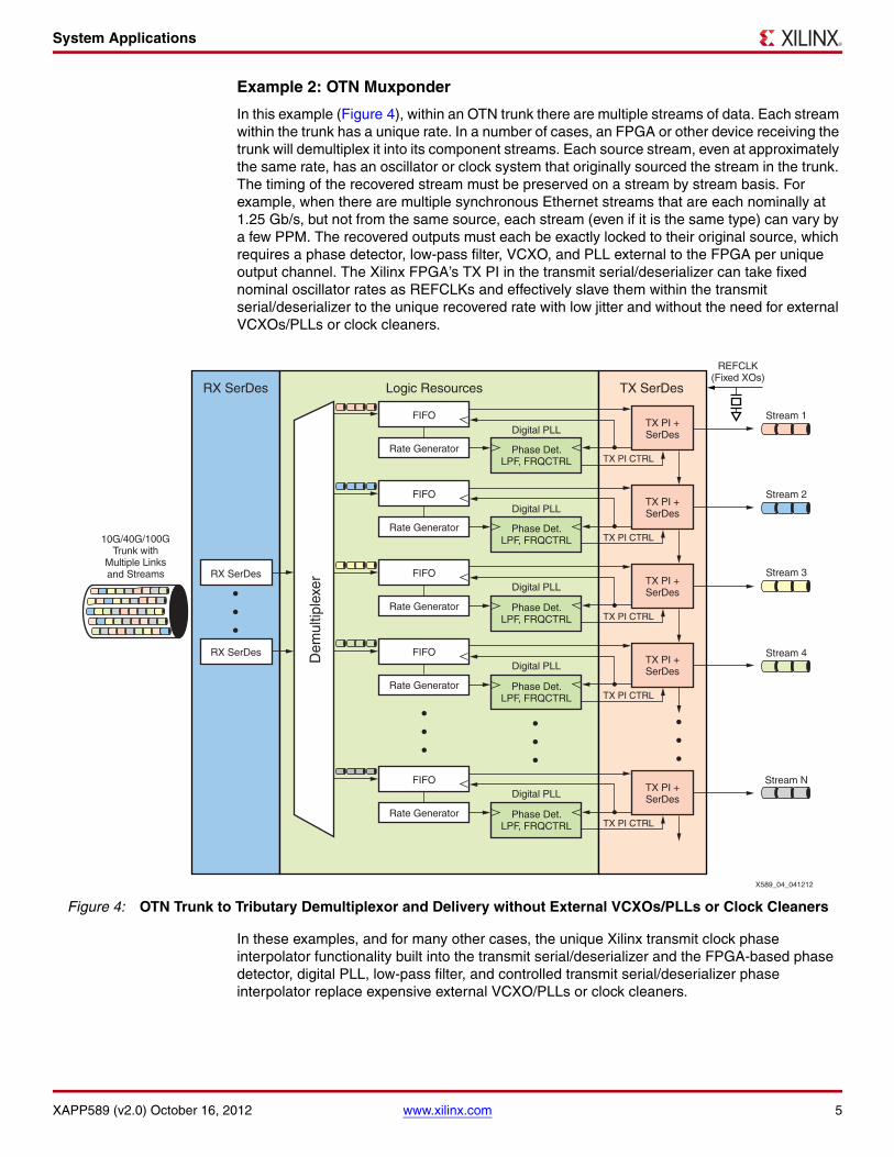
Figure 12 shows the transmit phase interpolator codes being written from the PICXO in the GTX transceiver. This demonstrates the frequency offset generation in progress. Figure 12 also reflects the direct phase shifting of the transmitter PLL at its operating frequency. The phase rotation shown results in a continuous phase ramp at the line rate. As a positive frequency is being generated, the phase is being continuously subtracted to generate shorter periods. The time unit is CEPI clocks.
When using the transmit phase interpolator in the GTX transceiver a general expectation is that the transmitter jitter will increase between 0.01 and 0.03 UI pk-pk due to the phase stepping and rotational nature of the modulator.
X-Ref Target - Figure 12
Figure 12: Chipscope Plot of PICXO Transmit Phase Interpolator Control When Locked
X589_12_092912
PICXO Measurements and Performance
XAPP589 (v2.0) October 16, 2012 www.xilinx.com 14
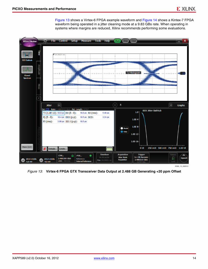
Figure 13 shows a Virtex-6 FPGA example waveform and Figure 14 shows a Kintex-7 FPGA waveform being operated in a jitter cleaning mode at a 9.83 GBs rate. When operating in systems where margins are reduced, Xilinx recommends performing some evaluations.
X-Ref Target - Figure 13
Figure 13: Virtex-6 FPGA GTX Transceiver Data Output at 2.488 GB Generating +20 ppm Offset
X589_13_092912

PICXO Measurements and Performance
XAPP589 (v2.0) October 16, 2012 www.xilinx.com 15
X-Ref Target - Figure 14
Figure 14: Kintex-7 FPGA GTX Transceiver Data Output at 9.83 GB Operating as a PICXO-based Jitter Cleaner at +32 ppm Offset
X589_14_100312
PICXO Measurements and Performance
XAPP589 (v2.0) October 16, 2012 www.xilinx.com 16
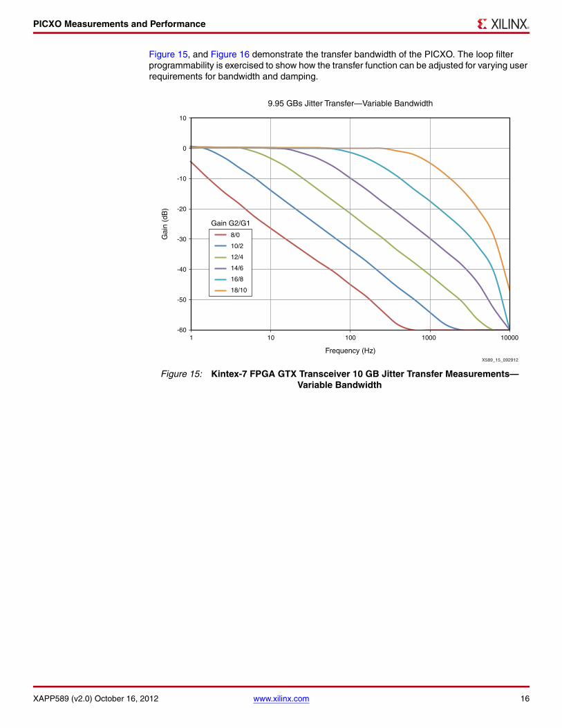
Figure 15, and Figure 16 demonstrate the transfer bandwidth of the PICXO. The loop filter programmability is exercised to show how the transfer function can be adjusted for varying user requirements for bandwidth and damping.
X-Ref Target - Figure 15
Figure 15: Kintex-7 FPGA GTX Transceiver 10 GB Jitter Transfer Measurements—Variable Bandwidth
X589_15_092912
10
0
-10
-20
-30
-40
-50
-60
Gai
n (d
B)
1 10 100
Frequency (Hz)
Gain G2/G1
8/0
10/2
12/4
14/6
16/8
18/10
9.95 GBs Jitter Transfer—Variable Bandwidth
1000 10000

PICXO Measurements and Performance
XAPP589 (v2.0) October 16, 2012 www.xilinx.com 17
X-Ref Target - Figure 16
Figure 16: Kintex-7 FPGA GTX Transceiver 10 GB Jitter Transfer Measurements—Variable Damping
5
3
1
-1
-3
-5
-7
-9
-11
-13
-15
Gai
n (d
B)
1 10 100
Frequency (Hz)
Gain G2/G1
16/15
16/15
16/13
16/12
16/11
16/9
16/8
9.95 GBs Jitter Transfer—Variable Damping
1000
X589_16_092912

PICXO Measurements and Performance
XAPP589 (v2.0) October 16, 2012 www.xilinx.com 18
For broadcast equipment, 270 Mb/s, 1.485 Mb/s, and 2.97 Mb/s are standard rates for SD-SDI, HD-SDI, and 3G-SDI. It is a challenge to meet the broadcast jitter requirements of all 3G-SDI formats. One of the 3G-SDI formats is 3G Level A. The examples in Figure 17 and Figure 18 are measurements showing the system passing with margin for 3G Level A SDI (3G Level A 1920 x 1080p at 59.94 Hz) in both 10 Hz and 100 KHz jitter measurement bandwidths, respectively. In this design, the VCXO and re-clocking function is incorporated completely in the FPGA using the PICXO scheme.
X-Ref Target - Figure 17
Figure 17: ML605 with SDI FMC board for a 3G Level A SDI Output of a Triple-Rate SDI Pass Through Design (at 10 Hz Jitter)
X589_18_092912

Physical Interface
XAPP589 (v2.0) October 16, 2012 www.xilinx.com 19
Physical Interface
Table 2 through Table 5 show the port definitions.
X-Ref Target - Figure 18
Figure 18: ML605 with SDI FMC board for a 3G Level A SDI Output of a Triple-Rate SDI Pass Through Design (at 100 KHz Jitter)
X589_19_092912
Table 2: Clocks, Reset, and Interface to the GTX Transceiver Ports
Signal Name Direction Description
RESET_I Input Synchronous reset. Active High
REF_CLK_I Input Reference clock, can be any clock (local, BUFG, pulse, etc.)
TXOUTCLKPCS_I InputVirtex-6 FPGAs: Connects directly to TXOUTCLKPCS of the GTX serial transceiver.Kintex-7 FPGAs: Same as TXOUTCLK_I.
TXOUTCLK_I Input Connects to TXOUTCLK of the GTX serial transceiver via a BUFG/BUFH/BUFR.
DRPEN_O Output Connects to the DEN port of the GTX serial transceiver.
DRPWEN_O Output Connects to the DWE port of the GTX serial transceiver.
DRPDATA_O [15:0] Output Connects to the DI port of the GTX serial transceiver.
DRPADDR_O [7:0] Output Connects to the DADDR port of the GTX serial transceiver.
DRPRDY_I Input Connects to the DRDY port of the GTX serial transceiver.

Physical Interface
XAPP589 (v2.0) October 16, 2012 www.xilinx.com 20
Table 3: DRP User Port
Signal Name Direction Description
DRP_USER_REQ_I Input Asserted to request DRP port access. Active High signal.
DRPEN_USER_I Input Same functionality as DEN GTX serial transceiver port [Ref 1] [Ref 4].
DRPWEN_USER_I Input Same functionality as DWEN GTX serial transceiver port [Ref 1] [Ref 4].
DRPADDR_USER_I [7:0] Input Same functionality as DADDR GTX serial transceiver port [Ref 1] [Ref 4].
DRPDATA_USER_I [15:0] Input Same functionality as DI GTX serial transceiver port [Ref 1] [Ref 4].
DRPRDY_USER_O Output This signal is a mirror of DRDY in the TXOUCLK domain. Indicates data present on DRPDO is valid [Ref 1][Ref 4].
DRPBUSY_O Output Indicates that the DRP port is not available to the user. Active High signal.
Table 4: Debug Ports
Signal Name Direction Description
ERROR_O [20:0] Output Output of phase detector. Signed number.
VOLT_O[21:0] Output Output of low-pass filter. Signed number.
DRPDATA_SHORT_O[7:0] Output Output of the accumulator. Unsigned number.
CE_PI_O Output Clock enable for accumulator.
CLKEN_O Output Clock enable for low pass filter and DAC.
RSTCNT_O Output Reset phase detector counters, load phase detector error into the low-pass filter.
OVF_PD Output Overflow in the phase detector.
OVF_AB Output Saturation of the low-pass filter inputs.
OVF_INT Output Saturation of the low-pass filter.
Physical Interface
XAPP589 (v2.0) October 16, 2012 www.xilinx.com 21
Operation
As shown in Figure 19, all input signals to the PICXO, except REF_CLK_I, must be synchronous to the rising edge of TXOUTCLK_I. The Virtex-6 FPGA GTX DRP interface is synchronous to TXOUTCLKPCS_I. The PICXO DRP arbiter takes care of the cross clock domain between the DRP user port and the GTX DRP port. The Kintex-7 FPGA GTX DRP interface is synchronous to TXOUTCLK_I.
To operate the DRP user port, the application asserts the DRP_USER_REQ_I signal and waits for DRP_BUSY_O to transition Low. Once DRP_BUSY_O is Low, the application can operate the DRP USER port as per the GTX DRP specification [Ref 1] [Ref 4]. All DRP user signals are synchronous to TXOUTCLK_I, including DRPRDY_USER_O. The application must keep DRP_USER_REQ_I asserted during a DRP transfer. Asserting DRP_USER_REQ_I stops the PICXO operation. Once the application is finished with the DRP accesses, the PICXO must be reset to restart correct operation. To reset and restart the PICXO it is sufficient to assert RESET_I High for one clock cycle.
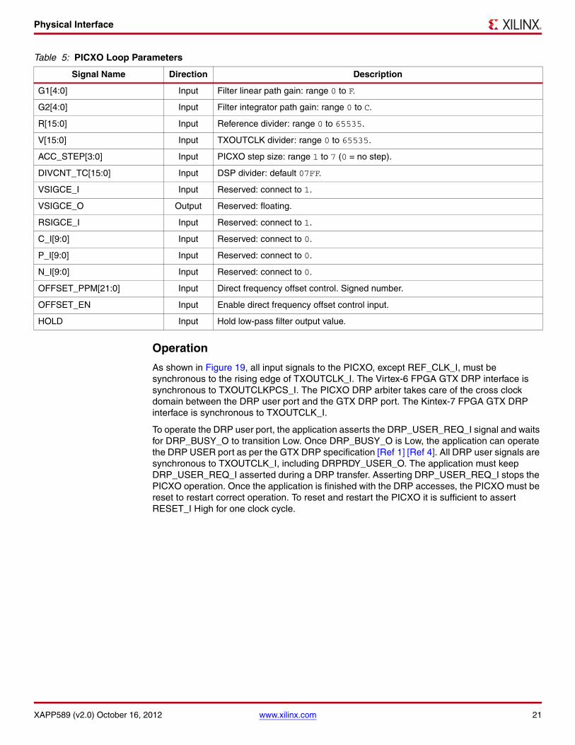
Table 5: PICXO Loop Parameters
Signal Name Direction Description
G1[4:0] Input Filter linear path gain: range 0 to F.
G2[4:0] Input Filter integrator path gain: range 0 to C.
R[15:0] Input Reference divider: range 0 to 65535.
V[15:0] Input TXOUTCLK divider: range 0 to 65535.
ACC_STEP[3:0] Input PICXO step size: range 1 to 7 (0 = no step).
DIVCNT_TC[15:0] Input DSP divider: default 07FF.
VSIGCE_I Input Reserved: connect to 1.
VSIGCE_O Output Reserved: floating.
RSIGCE_I Input Reserved: connect to 1.
C_I[9:0] Input Reserved: connect to 0.
P_I[9:0] Input Reserved: connect to 0.
N_I[9:0] Input Reserved: connect to 0.
OFFSET_PPM[21:0] Input Direct frequency offset control. Signed number.
OFFSET_EN Input Enable direct frequency offset control input.
HOLD Input Hold low-pass filter output value.

Implementation
XAPP589 (v2.0) October 16, 2012 www.xilinx.com 22
Implementation Constraints
A sample UCF file is provided with the reference design. Period constraints are necessary on TXOUTCLK, TXOUTCLKPCS, and REFCLK_I. The timing paths between TXOUTCLK and TXOUTCLKPCS must be TIG'ed. The necessary timing and implementation constraints are embedded into the PICXO netlist NGC file. If multiple instances of the PICXO are used in a design, the user must add a U_SET constraint for each instance. For example:
INST "Inst1/VCXO/*" U_SET = "Inst1_VCXO";INST "Inst2/VCXO/*" U_SET = "Inst2_VCXO";
All period constraints must be met. Errors on these listed timing constraints are acceptable, provided the error is less than 100 ps:
• TS_up_to_up_TIG
• TS_up_to_dn_TIG
• TS_dn_to_up_TIG
• TS_dn_to_dn_TIG
Virtex-6 FPGA Clocking
The PICXO (Figure 20) has two input clocks, TXOUTCLK_I and TXOUTCLKPCS_I, both driven from the GTX transceiver. The TXOUTCLK of the GTX transceiver must be connected to a BUFG before driving the TXOUTCLK_I input. The TXOUTCLKPCS_I must be driven directly from the GTX transceiver’s TXOUTCLKPCS. It is routed on the local routing. The XST VHDL attribute buffer_type, set to NONE, is used to prevent the automatic insertion of a BUFG on TXOUTCLKPCS_I (see the top-level example file).
X-Ref Target - Figure 19
Figure 19: Timing Waveform Examples
TXOUTCLK_1
DRP_USER_REQ_I
DRPBUSY_O
DRPEN_USER_I
DRPWEN_USER_I
DRPADDR_USER_I[7:0]
DRPDATA_USER_I[15:0]
DRPRDY_USER_O
RESET_I
0.0 ns 50.0 ns 100.0 ns 150.0 ns
X589_20_092912

Implementation
XAPP589 (v2.0) October 16, 2012 www.xilinx.com 23
Kintex-7 FPGA Clocking
The primary clocking scheme is detailed in Figure 21. The GTX transceiver TXOUTCLK connects to a BUFG which drives the PICXO inputs clocks TXOUTCLK_I and TXOUTCLKPCS_I as well as the GTX DRP clock DCLK.
A secondary clocking scheme is detailed in Figure 22. This clocking scheme can be used when TXOUTCLK exceeds the GTX DRP clock specifications. In this case, the GTX DRP clock must be an integer divisor of the TXOUTCLK frequency.
X-Ref Target - Figure 20
Figure 20: Virtex-6 FPGA PICXO Clocking
X-Ref Target - Figure 21
Figure 21: Kintex-7 FPGA Primary PICXO Clocking Scheme
X-Ref Target - Figure 22
Figure 22: Kintex-7 FPGA Secondary PICXO Clocking Scheme
GTX Transceiver BUFG/R
GTXREFCLK
TXOUTCLK
TXOUTCLKPCS
DCLK
TXOUTCLK_I
TXOUTCLKPCS_I
REFCLK_I
PICXO
X589_21_092912
GTX Transceiver BUFG/R/H
GTXREFCLK
TXOUTCLK
DCLK
TXOUTCLK_I
TXOUTCLKPCS_I
REFCLK_I
PICXO
X589_22_092912
GTX Transceiver BUFG/R/H
GTXREFCLK
TXOUTCLK
DCLK
TXOUTCLK_I
TXOUTCLKPCS_I
REFCLK_I
PICXO
PLL
X589_23_092912

Reference Design
XAPP589 (v2.0) October 16, 2012 www.xilinx.com 24
Mandatory Conditions and Limitations
• Transmit buffer bypass is not supported.
Virtex-6 FPGAs
• The GTX transceiver DRP clock (DCLK) must be directly connected to TXOUTCLKPCS without any buffer.
• TXPMAPHASEALIGN must be set to 1.
• The PMA_TX_CFG bit 17 must be set to 1.
• TXOUTCLKCTRL must be set to TXOUTCLKPMA_DIV2.
• The GTX transceiver must be set to a two byte-wide interface.
• TXOUTCLK and TXOUTCLKPCS must be the same frequency.
Kintex-7 FPGAs
• TXDLY_LCFG[2] and PCS_RSVD_ATTR[1] must be set to 1.
• The Kintex-7 FPGA ports TXPHALIGN, TXPHALIGNEN, and TXPHOVRDEN must be connected to 1.
• TXPHDLYPD must be connected to 0.
• TXOUTCLKSEL must be set to TXOUTCLKPMA (010)
Reference Design
The reference design is based on the Virtex-6 FPGA GTX transceiver wrapper v1.8 [Ref 3] and the Kintex-7 GTX transceiver wrapper v1.6 [Ref 5]. They target the ML605 and KC705 development platforms. They loop back the receive data to the transmitter. The PICXO instance locks the transmitter to the recovered clock RXRECLK.
Scripts (PICXO_V6_vhd.tcl, PICXO_V6_ver.tcl and PICXO_K7_vhd.tcl) are provided to help generate an ISE Design Suite project file, and implement and generate a bitstream. See the readme.txt for details.
A Chipscope Pro VIO core allows control of the PICXO loop parameters (Table 5). A Chipscope Pro ILA core monitors the PICXO debug signals (Table 4). The Chipscope Pro project files ML605_DT.cpj and K7.cpj, located in the src/chipscope folder, helps set up Chipscope Analyzer. The output error_o of the phase/frequency detector can be captured when rst_cnt_o is High to monitor the PICXO response. When locked, error_o should oscillate around 0, see Figure 11.
For Virtex-6 FPGA designs, two modules (double_reset and clock_detector) ensure correct operation after reset and loss of TXOUTCLK [Ref 2].
Table 6: Statistics and Performance Expectations for a Standalone PICXO
Target devices Virtex-6 LXT and Virtex-6 SXT FPGAs Kintex-7 FPGAs
LUTs 1060 1078
Registers 765 764
SRLs 2 1
Carry chains 19 19
Carry elements 498 498
MUXFXes 69 71
Maximum frequency Speed grade dependent, matches DRP port limit Speed grade dependent, matches DRP port limit

Reference Design
XAPP589 (v2.0) October 16, 2012 www.xilinx.com 25
Simulation of the example design is not supported. The GTX transceiver phase interpolator is not part of the GTX transceiver simulation model. The drp_arbiter source code is provided to enable functional simulation of DRP user access.
The reference design files are available for download at:
http://www.xilinx.com/member/vcxoff/index.htm
Table 7: Reference Design Checklist
Parameter Description
General
Developer name(s) David Taylor, Matt Klein, Vincent Vendramini
Target devicesVirtex-6 LXT XC6VLX240T FF1146 -1Kintex-7 XC7K325T FFG900 -1
Source code provided Yes
Source code format VHDL
Design uses code/IP from existing Xilinx application note/reference designs, CORE Generator™ software, or 3rd party
Yes
Simulation
Functional simulation performed No
Timing simulation performed No
Testbench used for functional and timing simulations No
Testbench format N/A
Simulator software/ version used N/A
SPICE/IBIS simulations N/A
Implementation
Synthesis software tools/version used XST, v13.4 and v14.2
Implementation software tools/versions used ISE Design Suite v13.4 and v14.2
Static timing analysis performed Yes
Hardware Verification
Hardware verified Yes
Hardware platform used for verification ML605, KC705

References
XAPP589 (v2.0) October 16, 2012 www.xilinx.com 26
References 1. UG360, Virtex-6 FPGA Configuration User Guide, see Dynamic Reconfiguration Port Chapter
2. EN142, Virtex-6 FPGA LX, LXT, SXT, and HXT Production Errata
3. UG366, Virtex-6 FPGA GTX Transceiver User Guide
4. UG470, 7 Series FPGAs Configuration User Guide, see Dynamic Reconfiguration Port Chapter.
5. UG476, 7 Series FPGA GTX/GTH Transceiver User Guide
Revision History
The following table shows the revision history for this document.
Table 8: Device Utilization and Performance
Virtex-6 FPGAs Kintex-7 FPGAs
Full Design Chipscope (ICON+VIO+ILA) Full Design Chipscope (ICON+VIO+ILA)
Slice LUTs 1600 600 1511 607
Slice Registers 1563 727 1512 733
Occupied slices(1) 1009 N/A 1035 683
Block RAM 15 15 15 15
BUFG 4 1 5 1
GTXE1 1 0 1 0
MMCM 0 0 0 0
Maximum Frequency DRP port limited to 150 MHz N/A DRP port limited
to 150 MHz N/A
Notes: 1. Number of occupied slices can vary depending on packing results.
Date Version Description of Revisions
05/08/12 1.0 Initial Xilinx release.
06/19/12 1.1 Updated to include Verilog version. Minor changes to the VHDL code in the Reference Design. Updated Table 5. Revised Block RAM in Table 8.
10/16/12 2.0 Added support for Kintex-7 FPGAs throughout document, including adding figures and revising tables. See new Reference Design information with updated design file.

Notice of Disclaimer
XAPP589 (v2.0) October 16, 2012 www.xilinx.com 27
Notice of Disclaimer
The information disclosed to you hereunder (the “Materials”) is provided solely for the selection and use ofXilinx products. To the maximum extent permitted by applicable law: (1) Materials are made available "ASIS" and with all faults, Xilinx hereby DISCLAIMS ALL WARRANTIES AND CONDITIONS, EXPRESS,IMPLIED, OR STATUTORY, INCLUDING BUT NOT LIMITED TO WARRANTIES OFMERCHANTABILITY, NON-INFRINGEMENT, OR FITNESS FOR ANY PARTICULAR PURPOSE; and (2)Xilinx shall not be liable (whether in contract or tort, including negligence, or under any other theory ofliability) for any loss or damage of any kind or nature related to, arising under, or in connection with, theMaterials (including your use of the Materials), including for any direct, indirect, special, incidental, orconsequential loss or damage (including loss of data, profits, goodwill, or any type of loss or damagesuffered as a result of any action brought by a third party) even if such damage or loss was reasonablyforeseeable or Xilinx had been advised of the possibility of the same. Xilinx assumes no obligation tocorrect any errors contained in the Materials or to notify you of updates to the Materials or to productspecifications. You may not reproduce, modify, distribute, or publicly display the Materials without priorwritten consent. Certain products are subject to the terms and conditions of the Limited Warranties whichcan be viewed at http://www.xilinx.com/warranty.htm; IP cores may be subject to warranty and supportterms contained in a license issued to you by Xilinx. Xilinx products are not designed or intended to befail-safe or for use in any application requiring fail-safe performance; you assume sole risk and liability foruse of Xilinx products in Critical Applications: http://www.xilinx.com/warranty.htm#critapps.
Automotive Applications Disclaimer
XILINX PRODUCTS ARE NOT DESIGNED OR INTENDED TO BE FAIL-SAFE, OR FOR USE IN ANY APPLICATION REQUIRING FAIL-SAFE PERFORMANCE, SUCH AS APPLICATIONS RELATED TO: (I) THE DEPLOYMENT OF AIRBAGS, (II) CONTROL OF A VEHICLE, UNLESS THERE IS A FAIL-SAFE OR REDUNDANCY FEATURE (WHICH DOES NOT INCLUDE USE OF SOFTWARE IN THE XILINX DEVICE TO IMPLEMENT THE REDUNDANCY) AND A WARNING SIGNAL UPON FAILURE TO THE OPERATOR, OR (III) USES THAT COULD LEAD TO DEATH OR PERSONAL INJURY. CUSTOMER ASSUMES THE SOLE RISK AND LIABILITY OF ANY USE OF XILINX PRODUCTS IN SUCH APPLICATIONS.