Phase Locked Loop Design as a Frequency...
71
Phase Locked Loop Design as a Frequency Multiplier A THESIS SUBMITTED IN PARTIAL FULFILLMENT OF THE REQUIREMENTS FOR THE DEGREE OF Master of Technology in VLSI Design and Embedded System By GEORGE TOM VARGHESE ROLL No: 207EC204 Department of Electronics and Communication Engineering National Institute Of Technology Rourkela 2007-2009
Transcript of Phase Locked Loop Design as a Frequency...

Phase Locked Loop Design as a Frequency
Multiplier
A THESIS SUBMITTED IN PARTIAL FULFILLMENT
OF THE REQUIREMENTS FOR THE DEGREE OF
Master of Technology
in
VLSI Design and Embedded System
By
GEORGE TOM VARGHESE
ROLL No: 207EC204
Department of Electronics and Communication Engineering
National Institute Of Technology
Rourkela
2007-2009

Phase Locked Loop Design as a Frequency
Multiplier
A THESIS SUBMITTED IN PARTIAL FULFILLMENT
OF THE REQUIREMENTS FOR THE DEGREE OF
Master of Technology
in
VLSI Design and Embedded System
By
GEORGE TOM VARGHESE
ROLL No: 207EC204
Under the Guidance of
Prof. KAMALAKANTA MAHAPATRA
Department of Electronics and Communication Engineering
National Institute Of Technology
Rourkela
2007-2009

National Institute Of Technology
Rourkela
CERTIFICATE
This is to certify that the thesis entitled, “Phase Locked Loop Design As A
Frequency Multiplier” submitted by George Tom Varghese in partial fulfillment
of the requirements for the award of Master of Technology Degree in Electronics
& Communication Engineering with specialization in “VLSI Design and
Embedded System” at the National Institute of Technology, Rourkela (Deemed
University) is an authentic work carried out by him under my supervision and
guidance.
To the best of my knowledge, the matter embodied in the thesis has not been
submitted to any other University / Institute for the award of any Degree or
Diploma.
Date: Prof. K. K. Mahapatra
Dept. of Electronics & Communication Engg.
National Institute of Technology
Rourkela-769008
i
ACKNOWLEDGEMENTS
This project is by far the most significant accomplishment in my life and it
would be impossible without people (especially my family) who supported me and
believed in me.
I am thankful to Dr. K. K. Mahapatra, Professor in the department of Electronics
and Communication Engineering, NIT Rourkela for giving me the opportunity to
work under him and lending every support at every stage of this project work. I
truly appreciate and value him esteemed guidance and encouragement from the
beginning to the end of this thesis. I am indebted to his for having helped me shape
the problem and providing insights towards the solution. His trust and support
inspired me in the most important moments of making right decisions and I am
glad to work with him.
I want to thank all my teachers Prof. S.K. Patra, Prof. G.Panda, Prof. G.S.
Rath, Prof. S. Meher, and Prof. D.P.Acharya for providing a solid background
for my studies and research thereafter.
I also very thankful to all my class mates and seniors of VLSI lab-I especially
Sushant Pattnaik, Dr. Jitendra K Das, Swain Ayas Kanta and K Sudeendra Kumar
who always encouraged me in the successful completion of my thesis work.
GEORGE TOM VARGHESE
ROLL No: 207EC204

ii
CONTENTS ABSTRACT ...........................................................................................................................................IV
LIST OF FIGURES ................................................................................................................................. V
ABBREVIATIONS USED ....................................................................................................................VII
INTRODUCTION ......................................................................................................................1
1.1 MOTIVATION .................................................................................................................................. 2
1.2 SYSTEM OVERVIEW ........................................................................................................................ 2
1.3 APPLICATIONS ................................................................................................................................ 4
1.4 LITERATURE REVIEW ...................................................................................................................... 4
PHASE FREQUENCY DETECTOR ..........................................................................................6
2.1 INTRODUCTION ............................................................................................................................... 7
2.2 PHASE DETECTOR AND PHASE FREQUENCY DETECTOR ................................................................... 7
2.3 LOW GLITCH HIGH SPEED CMOS PHASE FREQUENCY DETECTOR ................................................. 12
2.4 CHARACTERISTICS OF PFD ........................................................................................................... 17
CHARGE PUMP ...................................................................................................................... 21
3.1 INTRODUCTION ............................................................................................................................. 22
3.2 CHARGE PUMP CONFIGURATION ................................................................................................... 24
3.3 MODIFIED CHARGE PUMP ............................................................................................................. 27
LOOP FILTER ......................................................................................................................... 29
4.1 INTRODUCTION ............................................................................................................................. 30
4.2 TRANSFER FUNCTION OF PFD/CP/LPF .......................................................................................... 31
4.3 ADDITION OF RESISTANCE INTO THE LOOP FILTER ........................................................................ 34
4.4 ADDITION OF SECOND CAPACITOR INTO THE LOOP FILTER............................................................ 37
VOLTAGE CONTROLLED OSCILLATOR & DIVIDE BY COUNTER ................................ 38

iii
5.1 INTRODUCTION ............................................................................................................................... 39
5.2 CURRENT STARVED VCO ............................................................................................................. 41
5.3 PLL SPECIFICATIONS .................................................................................................................... 44
5.4 DIVIDE BY COUNTER..................................................................................................................... 45
5.5 PHASE LOCKED LOOP ................................................................................................................... 46
APPLICATIONS OF PLL & CONCLUSIONS ......................................................................... 48
6.1 CLOCK RECOVERY ........................................................................................................................ 49
6.2 CLOCK GENERATION .................................................................................................................... 49
6.3 FREQUENCY SYNTHESIS ................................................................................................................ 49
6.4 CONCLUSIONS .............................................................................................................................. 50
REFERENCES...................................................................................................................................... 51
LAYOUTS ............................................................................................................................................ 54

iv
ABSTRACT
High-performance digital systems use clocks to sequence operations and synchronize between
functional units and between ICs. Clock frequencies and data rates have been increasing with
each generation of processing technology and processor architecture. Phase locked-loops (PLLs)
are widely used to generate well-timed on-chip clocks in high-performance digital systems.
A PLL is a closed loop frequency system that locks the phase of an output signal to an
input reference signal. PLL‘s are widely used in computer, radio, and telecommunications
systems where it is necessary to stabilize a generated signal or to detect signals. The term ―lock‖
refers to a constant or zero phase difference between two signals. The signal from the feedback
path Df is compared to the input reference signal, INf until the two signals are locked. If the
phase is unmatched, this is called the unlocked state, and the signal is sent to each component in
the loop to correct the phase difference. These components consist of the Phase Frequency
Detector (PFD), the charge pump (CP), the low pass filter (LPF), the voltage controlled oscillator
(VCO) and divide by counter. The PFD detects any phase differences in Df and INf and then
generates an error signal. According to that error signal the CP either increases or decreases the
amount of charge to the LPF. This amount of charge either speeds up or slows down the VCO.
The loop continues in this process until the phase difference between Df and INf is zero or
constant—this is the locked mode. After the loop has attained a locked status, the loop still
continues in the process but the output of each component is constant. The output signal Df has
the same phase and/or frequency as INf .A divider can be used in the feedback path to synthesize a
frequency different than that of the reference signal.
The application I chose in designing the
PLL was a frequency synthesizer. A frequency synthesizer generates a frequency that can have a
different frequency from the original reference signal.

v
LIST OF FIGURES
Figure 1.Basic block diagram of a PLL .......................................................................................4
Figure2. XOR Phase Detector ....................................................................................................7
Figure 3. XOR Phase Detector with Phase Difference = 0 ...........................................................8
Figure 4.XOR Phase Detector with Phase Difference = Π/2 ........................................................9
Figure 5.XOR Phase Detector with Phase Difference = Π ...........................................................9
Figure 6.PD Characteristics Graph of Phase Difference ranging from 0 to 2Π ........................... 10
Figure 7.PFD Implementation ................................................................................................... 11
Figure 8.PFD Simulation I (A Leads B) .................................................................................... 11
Figure 9.PFD Simulation II (B Leads A) ................................................................................... 12
Figure 10.Negative Logic Resettable D flip-flop ....................................................................... 13
Figure 12.Positive Logic Resettable D flip-flop ......................................................................... 14
Figure 11.Zoomed view of CMOS PFD, when ―NAND‖ gate is used [glitch is from 25.06 ns to
25.26 ns]. .................................................................................................................................. 14
Figure 13.AND Gate implementation using Pass Transistor Logic ............................................ 15
Figure 14.Proposed PFD Implementation .................................................................................. 16
Figure 15.Zoomed View of Simulation of Proposed PFD .......................................................... 16
Figure 16.Simulation of Proposed PFD with 1ns Phase Difference ............................................ 17
Figure 17.Proposed PFD‘s 2 GHz Operation ............................................................................. 18
Figure 18.Generation of Coincident Pulses when the Phase Difference is Zero .......................... 19
Figure 19.Tristate Output Schematic ......................................................................................... 22
Figure 20.Tristate Output Simulation ........................................................................................ 23
Figure 21.Tristate Output VDD Variation Schematic................................................................. 23
Figure 22.Tristate Output VDD Variation Simulation ................................................................ 24
Figure 23.Charge Pump Configuration ...................................................................................... 25
Figure 24. Charge Pump Simulation .......................................................................................... 25
Figure 25.Charge Pump VDD Variation Schematic ................................................................... 26
Figure 26.Charge Pump VDD Variation Schematic ................................................................... 26
Figure 27.Modified Charge Pump Schematic ............................................................................ 27

vi
Figure 28.Modified Charge Pump Simulation with NMOS on ................................................... 28
Figure 29.Modified Charge Pump Simulation with PMOS on ................................................... 28
Figure 30.Loop Filter Schematic ............................................................................................... 30
Figure 31.Test of Linearity of PFD/CP/LPF Combination ......................................................... 31
Figure 32.Ramp Approximation of the Response ...................................................................... 32
Figure 33.Step Response of PFD/CP/LPF Combination ............................................................ 33
Figure 34.Linear Model of Simple Charge Pump PLL ............................................................... 34
Figure 35.Loop Gain Characteristics of Simple Charge Pump PLL and after the addition of zero
into the loop gain ...................................................................................................................... 35
Figure 36.Schematic of Loop Filter with R1 and C1 .................................................................. 36
Figure 37.Simulation of Loop Filter with R1 and C1 ................................................................. 36
Figure 38.Schematic of Loop Filter with R1, C1 and C2 ........................................................... 37
Figure 39. Simulation of Loop Filter with R1, C1 and C2 .......................................................... 37
Figure 40.A Five Stage Ring Oscillator ..................................................................................... 39
Figure 41.Differential Ring Oscillator ....................................................................................... 40
Figure 42.Regenerative Feedback System ................................................................................. 41
Figure 43.Current Starved VCO ................................................................................................ 42
Figure 44.Frequency Vs Control Voltage of Current Starved VCO ............................................ 43
Figure 45.Schematic of Divide by 64 Counter ........................................................................... 45
Figure 46.Simulation of Divide by 64 Counter .......................................................................... 45
Figure 47.Phase Locked Loop Schematic .................................................................................. 46
Figure 48.Simulation of 8.8 MHz .............................................................................................. 47
Figure 49.Simulation of 11.5 MHz ............................................................................................ 47

vii
ABBREVIATIONS USED
PLL Phase Locked Loop
PFD Phase Frequency Detector
CP Charge Pump
LPF Loop Filter
VCO Voltage Controlled Oscillator
controlV Control Voltage
XOR Exclusive OR
Damping Factor
LT Lock Time
n Natural Frequency
PDIK Charge Pump Gain
VCOK VCO Gain
NIT ROURKELA 1
Chapter 1
INTRODUCTION

NIT ROURKELA 2
1.1 Motivation
A PLL is essentially a feedback loop that locks the on-chip clock phase to that of an input
clock or signal. High-performance PLLs and clock buffers are widely used within a digital
system for two purposes: clock generation, and timing recovery. For clock generation, since off-
chip reference frequencies are limited by the maximum frequency of a crystal frequency
reference, (Typically in the range of 10 MHz) a PLL receives the reference clock and multiplies
the frequency to the multi-gigahertz operating frequency. The high-frequency clock is then
driven to all parts of the chip. Timing recovery pertains to the data communication between
chips. As data rates increase to satisfy the increase in on-chip processing rate, the phase
relationship between the input data and the on-chip clock is not fixed. To reliably receive the
high-speed data, a PLL locks the clock phase that samples the data to the phase of the input data.
Phase locked loop is closed loop control system that compares the output phase with the
input phase. High-performance digital systems use clocks to sequence operations and
synchronize between functional units and between ICs. Clock frequencies and data rates have
been increasing with each generation of processing technology and processor architecture.
Within the digital systems, well-timed clocks are generated with phase-locked loops (PLLs). The
rapid increase of the system‘s clock frequency possesses challenges in generating and
distributing the clock with low uncertainty.
1.2 System Overview
Phase-locked loops (PLLs) generate well-timed on-chip clocks for various applications such
as clock-and-data recovery, microprocessor clock generation and frequency synthesizer. The
basic concept of phase locking has remained the same since its invention in the 1930s. However,
design and implementation of PLLs continue to be challenging as design requirements of a PLL
such as clock timing uncertainty, power consumption and area become more stringent.
This section briefly discusses the basic concept of phase locking. A PLL is a closed-loop
feedback system that sets fixed phase relationship between its output clock phase and the phase
of a reference clock. A PLL tracks the phase changes that are within the bandwidth of the PLL.

NIT ROURKELA 3
A PLL also multiplies a low-frequency reference clock REFCK , to produce a high-frequency
clock OUTCK .
A PLL is a negative feedback control system circuit. As the name implies, the purpose of a
PLL is to generate a signal in which the phase is the same as the phase of a reference signal. This
is done after many iterations of comparing the reference and feedback signals. The overall goal
of the PLL is to match the reference and feedback signals in phase, this is the lock mode. After
this, the PLL continues to compare the two signals but since they are in lock mode, the PLL
output is constant.
A basic form of a PLL consists of five main blocks:
1. Phase Detector or Phase Frequency Detector (PD or PFD)
2. Charge Pump (CP)
3. Low Pass Filter (LPF)
4. Voltage Controlled Oscillator (VCO)
5. Divide by ‗N‘ Counter
The phase frequency detector (comparator) produces an error output signal based on the
phase difference between the phase of the feedback clock and the phase of the reference clock.
Over time, small frequency differences accumulate as an increasing phase error. If there is a
phase difference between the two signals, it generates ―up‖ or ―down‖ synchronized signals to
the charge pump/ low pass filter. If the error signal from the PFD is an ―up‖ signal, then the
charge pump pumps charge onto the LPF capacitor which increases the control voltage controlV . On
the contrary, if the error signal from the PFD is a ―down‖ signal, the charge pump removes
charge from the LPF capacitor, which decreases controlV . controlV is the input to the VCO. Thus, the
LPF is necessary to only allow DC signals into the VCO and is also necessary to store the charge
from the CP. The purpose of the VCO is to either speed up or slow down the feedback signal
according to the error generated by the PFD. If the PFD generates an ―up‖ signal, the VCO
speeds up. On the contrary, if a ―down‖ signal is generated, the VCO slows down. The frequency
of oscillation is divided down to the feedback clock by a frequency divider. The phase is locked
when the feedback clock has a constant phase error and the same frequency as the reference
clock. Because the feedback clock is a divided version of the oscillator‘s clock frequency, the
frequency of oscillation is N times the reference clock.

NIT ROURKELA 4
Figure 1.Basic block diagram of a PLL
1.3 Applications
The input of the PLL is a reference frequency, INf from the user. The VCO sends another
input frequency, Df into the PFD to compare the reference frequency with the VCO frequency.
After the PLL corrects the frequency to have zero offset phase, or to be in the lock mode, the
frequency is taken as an output at the VCO, Df . Therefore, a frequency is synthesized. (Note:
Constraints on the input frequency INf must be within the tuning range of the VCO and the PLL
as a whole system. The tuning range is the range in which the VCO functions properly. If INf
isn‘t within this tuning range, a divider is necessary). A divider can be used in the feedback path
to synthesize a frequency different than that of the reference signal. Furthermore, since the
reference signal is a clock signal, the output is also a clock signal—thus a clock generator.
1.4 Literature Review
There are mainly two types of phase detectors are used in PLL.
1) XOR phase detector
2) Phase frequency detector

NIT ROURKELA 5
The XOR phase detector is simply exclusive OR gate. Depending upon the phase difference
between the inputs varies, so width of the output pulses, thereby providing a dc level
proportional to the phase difference between the inputs. While the XOR circuit produces error
pulses on both rising and falling edges (The phase frequency detector will respond only to
positive or negative transitions). The operation of phase detectors is similar to that of differential
amplifiers in that both sense the difference between the inputs, generating a proportional output.
The average phase detector output contains little frequency information and no valuable phase
information. Since the phase detector is insensitive to frequency difference at the input, upon
start-up when the oscillator‘s frequency divided by N is far from the reference frequency, the
PLL may fail to lock. The problem is known as an inadequate acquisition range of the PLL. To
remedy the problem, a phase-frequency detector (PFD) is used that can detect both phase and
frequency differences.
The output of the PFD should be combined into a single output for driving the loop filter.
There are two methods of doing this. The first method is called tri-state output. The second
configuration is charge pump.
The loop filter is the brain of PLL. If the loop filter values are not selected correctly, it
may take the loop too long to lock, or once locked small variations in the input data may cause
the loop to unlock.
There are mainly two types of voltage controlled oscillators used in PLL. The source
coupled VCO can be designed to dissipate less power than the current starved VCO. The major
disadvantage of this configuration is the need of a capacitor. However this configuration is useful
when the VCO center frequency is set by an external capacitor. The operation of current starved
VCO is similar to the ring oscillator.
We design the VCO in such a way that the output of VCO is ‗N‘ times the reference
frequency. So the output of the VCO is passed through a divide by ‗N‘ counter and feedback to
the input.

NIT ROURKELA 6
CHAPTER 2
PHASE FREQUENCY DETECTOR

PHASE LOCKED LOOP DESIGN AS A FREQUENCY MULTIPLIER
NIT ROURKELA 7
2.1 Introduction
The phase frequency detector, PFD, measures the difference in phase between the reference and
feedback signals. If there is a phase difference between the two signals, it generates ―up‖ or
―down‖ synchronized signals to the charge pump/ low pass filter. If the error signal from the
PFD is an ―up‖ signal, then the charge pump pumps charge onto the LPF capacitor which
increases the control voltage controlV . On the contrary, if the error signal from the PFD is a ―down‖
signal, the charge pump removes charge from the LPF capacitor, which decreases controlV . controlV
is the input to the VCO. Thus, the LPF is necessary to only allow DC signals into the VCO and is
also necessary to store the charge from the CP. The purpose of the VCO is to either speed up or
slow down the feedback signal according to the error generated by the PFD. If the PFD generates
an ―up‖ signal, the VCO speeds up. On the contrary, if a ―down‖ signal is generated, the VCO
slows down. The output of the VCO is then fed back to the PFD in order to recalculate the phase
difference, thus creating a closed loop frequency control system.
2.2 Phase Detector and Phase Frequency Detector
A phase detector is a circuit that detects the difference in phase between its two input
signals. An example of a basic phase detector is the XOR gate. It produces error pulses on both
falling and rising edges. a detailed analysis of the XOR PD when the reference and feedback
signals are out of phase by zero, Π/2, and Π respectively.
Figure2. XOR Phase Detector
vco
ref
ref
avgV

PHASE LOCKED LOOP DESIGN AS A FREQUENCY MULTIPLIER
NIT ROURKELA 8
Figure 3. XOR Phase Detector with Phase Difference = 0
In Figure 3, the phase difference between the two signals is zero—locked phase. The average
output avgV , from the XOR gate is zero for this case. The XOR input/output characteristic graph
is a plot of avgV versus the phase difference. Figures 4 and 5 represent the phase difference for
Π/2, and Π. The XOR PD characteristic plot is shown in figure 6.

PHASE LOCKED LOOP DESIGN AS A FREQUENCY MULTIPLIER
NIT ROURKELA 9
Figure 4.XOR Phase Detector with Phase Difference = Π/2
Figure 5.XOR Phase Detector with Phase Difference = Π

PHASE LOCKED LOOP DESIGN AS A FREQUENCY MULTIPLIER
NIT ROURKELA 10
Figure 6.PD Characteristics Graph of Phase Difference ranging from 0 to 2Π
The XOR PD as shown above in Figure is a very simple implementation of a PD, however; its
major disadvantage is that it can lock onto harmonics of the reference signal and most
importantly it cannot detect a difference in frequency.
To take care of these disadvantages, we implemented the Phase
Frequency Detector, which can detect a difference in phase and frequency between the reference
and feedback signals. Also, unlike the XOR gate PD, it responds to only rising edges of the two
inputs and it is free from false locking to harmonics. Furthermore, the PFD outputs either an
―QA‖ or a ―QB‖ to the CP. The PFD design uses two flip flops with reset features. The inputs to
the two clocks are the reference and feedback signals. The D inputs are connected to VDD—
always remaining high. The outputs are either ―QA‖ or ―QB‖ pulses. These outputs are both
connected to an AND gate to the reset of the D-FF‘s. When both QA and QB are high, the output
through the AND gate is high, which resets the flip flops. Thus both signals cannot be high at the
same time. This means that the output of the PFD is either an up or down pulse—but not both.
The difference in phase is measured by whichever rising edge occurs first.

PHASE LOCKED LOOP DESIGN AS A FREQUENCY MULTIPLIER
NIT ROURKELA 11
Figure 7.PFD Implementation
The PFD circuit can be analyzed in two different ways. One way in which A leads B and the
other in which B leads A.
Figure 8.PFD Simulation I (A Leads B)

PHASE LOCKED LOOP DESIGN AS A FREQUENCY MULTIPLIER
NIT ROURKELA 12
The QA pulse is the difference between the phases of the two clock signals. This QA pulse
indicates to the rest of the circuit that the feedback signal needs to speed up or ―catch up‖ with
the reference signal. In the second case B is leading A. In this QB pulse represents the difference
between the phases of the two clock signals. Figure 9 represents B leads A simulation results.
Figure 9.PFD Simulation II (B Leads A)
2.3 Low Glitch High Speed CMOS Phase Frequency
Detector
The phase frequency detector generates the error signal corresponding to the difference
between phase or frequency of the reference input and the feedback output. The PFD has two
outputs. In order to combine two outputs into a single output, the charge pump is used. The
output of the charge pump is directly connected to the loop filter. The function of the loop filter

PHASE LOCKED LOOP DESIGN AS A FREQUENCY MULTIPLIER
NIT ROURKELA 13
is to filter out the high frequency components from the PFD output. The voltage controlled
oscillator accepts the control voltage from the loop filter and generates the oscillating output.
The VCO output is feedback to the input through a divide by counter. The process is continued
until both the input signals are synchronized or locked. In this we introduce a new CMOS PFD
with low glitch. The low glitch is achieved by using a pass transistor ―AND‖ gate instead of
CMOS gate. With the usage of negative logic resettable D flip-flop in the design, the
functionality of PFD can be achieved with the help of ―NAND‖ gate instead of ―AND‖ gate
[Fig 10].
QA
Clock
D
Reset
Figure 10.Negative Logic Resettable D flip-flop
The inputs to the PFD are two signals which are having a period of 100 ns and with a
phase difference of 90º (25 ns). Since CMOS logic consumes very low power, the PFD having a
power dissipation of 2.089 µW in 90 nm technology with Vdd=1.8 V. The glitch at the output of
PFD is more is the disadvantage of this circuit [Fig 11]. The duration of glitch in the PFD is 200
ps [25.06 ns to 25.26 ns]. If the glitch is more at the output of PFD, the reset time of the flip-flop
is also more. Effectively the duration of glitch is a factor which determines the speed of the PFD.
In order to reduce the glitch as well as increase the speed of PFD, a new low glitch CMOS PFD
is proposed, but with more power dissipation.
QA'

PHASE LOCKED LOOP DESIGN AS A FREQUENCY MULTIPLIER
NIT ROURKELA 14
For the reduction of glitch at the output of PFD, pass transistor ―AND‖ gate is used in the
implementation. For that purpose, conversion of negative resettable D flip-flop to positive
resettable D flip-flop is required. This is achieved with the addition of a single inverter at the
―reset‖ terminal of the implementation [Fig 12].
Clock
D
Reset
Figure 12.Positive Logic Resettable D flip-flop
QA
QA'
Figure 11.Zoomed view of CMOS PFD, when “NAND” gate is used [glitch is
from 25.06 ns to 25.26 ns].

PHASE LOCKED LOOP DESIGN AS A FREQUENCY MULTIPLIER
NIT ROURKELA 15
Since normal and inverted outputs are available in the D flip-flop, effectively only two
extra transistors are required for implementing ―and‖ gate using pass transistor logic [Fig 13]. In
this gate, if the B input is high, the top transistor is turned on and copies the input A to the output
F. When B is low, the bottom pass transistor is turned on and passes a logic zero. The presence
of switch B' is essential to ensure a low impedance path to the supply rails under all
circumstances. The NMOS device is effective at passing a zero logic, but it is poor at pulling a
node to logic one. Whenever a pass transistor pulls a node high, the output only charges up to
Vdd-threshold voltage of NMOS.
Figure 13.AND Gate implementation using Pass Transistor Logic
But in the proposed PFD, this voltage is sufficient to enable the reset pin of the flip-flop. So
functionality is achieved correctly. The gate delay in the feedback path is reduced by a factor of
two in the proposed PFD as compared to the previous circuit. [Total number of gates in the
feedback path is four [CMOS ―NAND‖] in the previous PFD]. Totally the proposed PFD [Fig
14] having a power dissipation of 3.047 µW in 90 nm technology with Vdd=1.8 V with a
reduced glitch. The inputs to the proposed PFD are the same signals that applied to the prior
circuit. The outputs of the two PFD‘s are similar without zooming. The zoomed view establishes
the advantage of the proposed PFD over the prior circuit. The duration of glitch is only 140 ps.
[25.06 ns to 25.20 ns] Fig 15.
F=A.B
B'
B
A

PHASE LOCKED LOOP DESIGN AS A FREQUENCY MULTIPLIER
NIT ROURKELA 16
Vdd
Vdd
Figure 14.Proposed PFD Implementation
A
B
Pass Transistor ―And‖
Gate
D
QA
Clock QA'
RESET QA'
D
QB
Clock
RESET
Figure 15.Zoomed View of Simulation of Proposed PFD

PHASE LOCKED LOOP DESIGN AS A FREQUENCY MULTIPLIER
NIT ROURKELA 17
The reduction in the duration of the glitch will reduce the reset time of the flip-flops also.
The reset time is one of the factors which determine the speed of the PFD. As the reset time
decreases, speed of PFD will increase. Since reset time of the proposed PFD is less, the speed of
the PFD increases.
2.4 Characteristics of PFD
Phase sensitivity, maximum operating frequency and dead zone region are the
characteristics of any PFD. Sensitivity of PFD means the smallest difference the PFD can detect
and produce corresponding correct output signals, this leads to a conclusion that the higher the
sensitivity, the better the PFD. The proposed PFD is sensitive to even very small phase
differences [Upto1 ns] [Fig 16].
The definition of maximum operating frequency is defined as one over the shortest period
with correct PFD output signals when the inputs have the same frequency and 90º phase
difference. This definition is most suitable for flip-flop based PFD where this frequency can be
easily identified. The maximum operating frequency is inversely proportional to the reset pulse
Figure 16.Simulation of Proposed PFD with 1ns Phase Difference

PHASE LOCKED LOOP DESIGN AS A FREQUENCY MULTIPLIER
NIT ROURKELA 18
width of the circuit. Since reset pulse width is less in the proposed PFD, it can be operated over a
higher range than the prior PFD. The proposed PFD can operate up to 2 GHz [Fig 17].
A hypothetical PFD produces no pulses for a zero input phase difference. Whenever a
small phase error comes, due to finite rise time and fall time, the output of PFD pulse may not
find enough time to reach a logical high level. When the phase error is within the dead zone, the
control system does not change the control voltage. In other words, if the input phase difference
falls below a certain value, the output voltage of the PFD is no longer a function of phase
difference. If the phase difference is below the threshold level, the charge pump injects no
current. The dead zone is highly undesirable because it allows the VCO to accumulate random
phase error with respect to the input while receiving no corrective feedback. The proposed PFD
generates narrow, coincident pulses on both QA and QB even when the phase difference is zero
[Fig 18]. Effectively the coincident pulses on QA and QB can eliminate the dead zone.
Figure 17.Proposed PFD’s 2 GHz Operation

PHASE LOCKED LOOP DESIGN AS A FREQUENCY MULTIPLIER
NIT ROURKELA 19
A high speed low glitch CMOS phase frequency detector is proposed in 90 nm
technology with Vdd=1.8 V in Cadence tool. . Proposed new circuit uses ―AND‖ gate using pass
transistor logic rather than conventional CMOS logic. The usage of pass transistor reduces the
glitch at the output of the PFD. The proposed PFD is having a better phase sensitivity, no dead
zone and a higher frequency of operation. Simulation results shows that the proposed PFD has
low glitch as compared to conventional PFD. So the speed of the proposed PFD is also high. The
proposed PFD can be used in PLL applications such as frequency multiplier, clock recovery
purposes.
Figure 18.Generation of Coincident Pulses when the Phase Difference is Zero

PHASE LOCKED LOOP DESIGN AS A FREQUENCY MULTIPLIER
NIT ROURKELA 20
Table I
Comparison Conventional PFD Proposed PFD
Technology 90 nm 90 nm
Vdd 1.8 V 1.8 V
Current 1.160 µA 1.693 µA
Power Dissipation 2.089 µW 3.047 µW
Dead Zone Zero Zero
Reset Time 200 ps 140 ps
Glitch 25.06 ns to 25.26 ns 25.06 ns to 25.20 ns

PHASE LOCKED LOOP DESIGN AS A FREQUENCY MULTIPLIER
NIT ROURKELA 21
CHAPTER 3
CHARGE PUMP

PHASE LOCKED LOOP DESIGN AS A FREQUENCY MULTIPLIER
NIT ROURKELA 22
3.1 Introduction
The output of the PFD should be combined into a single output for driving the loop filter. There
are two methods of doing this. The first method is called tri-state output. When both signals are
low, both mosfets are off and the output is in a high impedance state. If the QA signal goes high,
PMOS turns on and pulls the output to VDD while if the QB is high, the output is pulled low
through NMOS. The main problem that exists with this configuration is that the power supply
variation can significantly affect the output voltage when PMOS is on. Figure 19 and 20
represents tri-state output configuration and simulation.
Figure 19.Tristate Output Schematic
Next I am discussing about the VDD variation in the tri-state output. Suppose VDD
changes to 1.75 instead of 1.8. Then figure 22 represents how the circuit will behave to
this condition and figure 21 represents the corresponding schematic diagram.

PHASE LOCKED LOOP DESIGN AS A FREQUENCY MULTIPLIER
NIT ROURKELA 23
Figure 20.Tristate Output Simulation
Figure 21.Tristate Output VDD Variation Schematic

PHASE LOCKED LOOP DESIGN AS A FREQUENCY MULTIPLIER
NIT ROURKELA 24
Figure 22.Tristate Output VDD Variation Simulation
3.2 Charge Pump Configuration
The second configuration is charge pump. When the PFD QA signal goes high, NMOS turns on,
connecting the current source to the loop filter. Since the current source can be made insensitive
to supply variation, modulation of VCO control voltage is absent. In order to adjust the delay
between QA and QB, a complimentary pass gate is added into the circuit between QB and the
upper NMOS. The UP and DOWN switches, M4 and M3, operate in the triode region and they
act like resistors (thermal noise occurs). They should have a large W/L ratio for faster switching
time and wider voltage range. When the W/L ratio (transistor size) is large, the on resistance will
be small. As the resistance is smaller, the voltage across the resistor will be small, that will allow
for a wider voltage range at the output. The transistors M2 and M1 are current mirror sources and
sinks.

PHASE LOCKED LOOP DESIGN AS A FREQUENCY MULTIPLIER
NIT ROURKELA 25
Figure 23.Charge Pump Configuration
Figure 24. Charge Pump Simulation

PHASE LOCKED LOOP DESIGN AS A FREQUENCY MULTIPLIER
NIT ROURKELA 26
In this section, I describes about the VDD variation of charge pump. By comparing with the tri-
state configuration we can conclude that the charge pump configuration is less affected by the
VDD variation. So the charge pump configuration is used in the PLL.
Figure 25.Charge Pump VDD Variation Schematic
Figure 26.Charge Pump VDD Variation Schematic

PHASE LOCKED LOOP DESIGN AS A FREQUENCY MULTIPLIER
NIT ROURKELA 27
3.3 Modified Charge Pump
In this section, I am changing the current source in the default charge pump to another
current source for better operation. That means to ensure that mosfets are in saturation.
Figure 27.Modified Charge Pump Schematic
The charge pump consists of two switched current sources that pump charge into or out
of the loop filter according to two logical inputs. The circuit has three states. If QA=0, QB=0,
then both switches are off and output voltage remains constant. If QA=1, QB=0, then current
through the PMOS branch charges the capacitor. Conversely if QA=0, QB=1, then current
through the PMOS branch discharges the capacitor. If for example, A leads B, then QA
continues to produce pulses and output rises steadily. Conversely B leads A, then QB continues
to produce pulses and output falls steadily. The currents through the PMOS branch and NMOS
branch are nominally equal.

PHASE LOCKED LOOP DESIGN AS A FREQUENCY MULTIPLIER
NIT ROURKELA 28
Figure 28.Modified Charge Pump Simulation with NMOS on
Figure 29.Modified Charge Pump Simulation with PMOS on

PHASE LOCKED LOOP DESIGN AS A FREQUENCY MULTIPLIER
NIT ROURKELA 29
CHAPTER 4
LOOP FILTER

PHASE LOCKED LOOP DESIGN AS A FREQUENCY MULTIPLIER
NIT ROURKELA 30
4.1 Introduction
The loop filter is the brain of PLL. If the loop filter values are not
selected correctly, it may take the loop too long to lock, or once locked small variations in the
input data may cause the loop to unlock. The PFD/CP/LP combination contains a pole at the
origin and VCO also contains a pole at the origin. So the instability arises because the loop gain
has two poles at the origin. In order to stabilize the system, we must modify the phase
characteristics by adding a resistor in series with the loop filter capacitor. The compensated PLL
also suffers from a critical drawback. Since the charge pump drives the series combination of R1
and C1, each time a current is injected into the loop filter, the control voltage experiences a large
jump. To relax this issue, a second capacitor is usually added in parallel with R1 and C1.
Figure 30.Loop Filter Schematic

PHASE LOCKED LOOP DESIGN AS A FREQUENCY MULTIPLIER
NIT ROURKELA 31
4.2 Transfer Function of PFD/CP/LPF
In order to quantify the behavior of charge pump PLLs, we must develop a linear model for the
combination of the PFD, the charge pump and the low pass filter, thereby obtaining the transfer
function. We therefore raise two questions: (1) Is the PFD/CP/LPF combination is a linear
system? (2). If so, how can the transfer function can be computed?
To answer the first question, we test the system for linearity. For example, if we double
the input phase difference and see if outV exactly doubles.
Figure 31.Test of Linearity of PFD/CP/LPF Combination

PHASE LOCKED LOOP DESIGN AS A FREQUENCY MULTIPLIER
NIT ROURKELA 32
The flat sections of outV double, but not the ramp sections. After all, the current charging or
discharging C1 is constant, yielding a constant slope for the ramp. Thus the system is not linear
in the strict sense. To overcome this problem, we approximate the output waveform by a ramp
arriving at a linear relationship between outV and . In a sense, we approximate a discrete time
system by a continuous time model.
To answer the second question, we recall that the
transfer function is the Laplace transform of the impulse response, requiring that we apply a
phase difference impulse and compute outV in the time domain. Since a phase difference impulse
is difficult to visualize, we apply a phase difference step, obtain outV , and difference the result
with respect to time.
Figure 32.Ramp Approximation of the Response
To answer the second question, we recall that the transfer function is the Laplace
transform of the impulse response, requiring that we apply a phase difference impulse and
compute outV in the time domain. Since a phase difference impulse is difficult to visualize, we
apply a phase difference step, obtain outV , and difference the result with respect to time.
Let us assume the input period is inT and the charge pump provides a current of PI to
the capacitor. We begin with a zero phase difference and at t=0, step the phase of B by 0 , =
0 u(t). As a result, QA or QB continues to produce pulses that are 2
0 inT seconds wide,

PHASE LOCKED LOOP DESIGN AS A FREQUENCY MULTIPLIER
NIT ROURKELA 33
raising the output voltage by
2
0 in
P
P T
C
I in every period. Approximated by a ramp, outV thus
exhibits a slope of
2
0
P
P
C
I and can be expressed as
outV (t)= tC
I
P
P
2 0 u (t)
The impulse response is therefore given by
)(thP
P
C
I
2U (t)
Yielding the transfer function
Figure 33.Step Response of PFD/CP/LPF Combination
SC
Is
V
P
Pout 1
2)(

PHASE LOCKED LOOP DESIGN AS A FREQUENCY MULTIPLIER
NIT ROURKELA 34
Consequently, the PFD/CP/LPF combination contains a pole at the origin, a point of contrast to
the PD/LPF circuit used in the type I PLL. In analogy with the expressionS
KVCO , we call P
P
C
I
2
the gain of the PFD and denote it by PFDK . Figure 34 represents the linear model of simple
charge pump PLL. After constructing a linear model of PLL, the open loop transfer function is
Figure 34.Linear Model of Simple Charge Pump PLL
4.3 Addition of Resistance into the Loop Filter
Since the loop gain has two poles at origin, this topology is called a type II PLL. The
closed loop transfer function denoted by
pC
vcoKpIS
pC
vcoKpI
sH
2
2
2)(
The result is alarming because the closed loop system contains two imaginary poles at
pC
vcoKpIjS
22,1
22 S
K
ΠC
I(S)|open
Φ
Φ VCO
P
P
IN
OUT

PHASE LOCKED LOOP DESIGN AS A FREQUENCY MULTIPLIER
NIT ROURKELA 35
So the system is unstable. The instability arises because the loop gain has only two poles at the
origin (Two ideal integrators). Each integrator contributes a constant phase shift of 90º, allowing
the system to oscillate at gain cross over frequency.
In order to stabilize the system, we must modify the phase characteristic such that the phase shift
is less than 180º at the gain cross over. This is accomplished by introducing a zero in to the loop
gain. That is by adding a resistor in series with the loop filter capacitor.
Now the transfer function becomes
Figure 35.Loop Gain Characteristics of Simple Charge Pump PLL and after the addition of
zero into the loop gain
S
K
SCR
IopenS VCO
P
PP
IN
OUT )1
(2
|)(

PHASE LOCKED LOOP DESIGN AS A FREQUENCY MULTIPLIER
NIT ROURKELA 36
Figure 36.Schematic of Loop Filter with R1 and C1
Figure 37.Simulation of Loop Filter with R1 and C1

PHASE LOCKED LOOP DESIGN AS A FREQUENCY MULTIPLIER
NIT ROURKELA 37
4.4 Addition of Second Capacitor into the Loop Filter
This circuit also suffers from a critical drawback. Since the charge pump drives the series
combination of R1 and C1, each time a current is injected into the loop filter, the control voltage
experience a large jump. To relax this issue, a second capacitor is added in parallel with R1 and
C1. The value of C2 is about one-fifth to one tenth of C1.
Figure 38.Schematic of Loop Filter with R1, C1 and C2
Figure 39. Simulation of Loop Filter with R1, C1 and C2

PHASE LOCKED LOOP DESIGN AS A FREQUENCY MULTIPLIER
NIT ROURKELA 38
CHAPTER 5
VOLTAGE CONTROLLED
OSCILLATOR & DIVIDE BY
COUNTER

PHASE LOCKED LOOP DESIGN AS A FREQUENCY MULTIPLIER
NIT ROURKELA 39
5.1 Introduction An oscillator is an autonomous system that generates a periodic output without any input. A
CMOS ring oscillator shown in Figure 40 is an example of an oscillator. So that the phase of a
PLL is adjustable, the frequency of oscillation must be tunable. In the example of an inverter ring
oscillator, the frequency could easily be adjusted with controlling the supply (voltage or current)
of inverters. The slope of frequency versus control signal curve at the oscillation frequency is
called voltage-to-frequency (or current to- frequency) conversion gain. Ideally, for the linear
analysis to apply over a large frequency range, the voltage gain of the VCO needs to be relatively
constant. The purpose of the VCO is to vary an output frequency proportional to the control
voltage input.
Figure 40.A Five Stage Ring Oscillator
There were two types of VCO architectures considered in this design. The first was a single-
ended ring oscillator, as shown in Figure 33. This design can be only by an odd number of
inverters.
delayNoscf
2
1
As Equation states, the oscillation frequency of this configuration is proportional to the number
of stages and the delay of each cell. While the single-ended ring oscillator is very simple in
design, it does have some major drawbacks. First, it requires the use of an odd number of
inverters in order for the circuit to not latch up. The main difficulty for using submicron CMOS
ring oscillators in wireless communication systems is their relatively poor phase noise response.
Due to these drawbacks, a differential ring oscillator was then considered. The main reason for
choosing a differential architecture was because it offered better noise rejection.

PHASE LOCKED LOOP DESIGN AS A FREQUENCY MULTIPLIER
NIT ROURKELA 40
Figure 41.Differential Ring Oscillator
As shown, there is an inversion between the third and fourth stages due to an even number of
stages being used. The oscillation frequency equation of the differential ring oscillator is the
same as the single-ended configuration shown in the previous Equation. The difference between
the two designs is that the differential architecture offers more flexibility in changing the
oscillation frequency because it is not restricted to having an odd number of stages. This is also
another advantage over using a single-ended architecture.
An oscillator is a circuit that produces a periodic signal, without any specific input signal except
internal noise. An oscillator can be viewed as a feedback system, figure 35 with a transfer
function of
)(1
)(
sH
sH
inV
outV
If H(s) = -1 then the gain would approach infinity, which results in infinity amplification of the
noise component at the oscillation frequency. For oscillation at one specific frequency two
criteria are stated. The first criterion is that the total phase shift around the loop is 180°. The
second criterion is that the feedback system amplifies its own noise at the frequency of
oscillation. These criteria mean that the returning signal is a negative replica of the input signal,
which will give a larger difference between the input signal and the feedback signal when
subtracting. The circuit is said to regenerate. At some point the amplitude of the regenerating
feedback system will be limited and the Barkhausen criteria of a gain=1 is fulfilled and gives a
stable oscillation.

PHASE LOCKED LOOP DESIGN AS A FREQUENCY MULTIPLIER
NIT ROURKELA 41
Figure 42.Regenerative Feedback System
In many applications it is desirable to have the ability to tune the oscillator to different
frequencies. The required VCO tuning range is mainly due to two factors. First, the tuning range
must be large enough to compensate for the change in VCO centre frequency due to process and
temperature variations. Second, any additional tuning required by the intended application must
be added.
5.2 Current Starved VCO
Most applications require that oscillators be ―tunable. i.e., their output frequency be a
function of a control input, usually a voltage. An ideal voltage-controlled oscillator is a circuit
whose output frequency is a linear function of its control voltage. There are different types of
voltage controlled oscillators used in PLL. Here I am discussing about 2 types of VCOs. Source
coupled VCO and Current starved VCO. The source coupled VCO can be designed to dissipate
less power than the current starved VCO. The major disadvantage of this configuration is the
need of a capacitor. However this configuration is useful when the VCO center frequency is set
by an external capacitor. The operation of current starved VCO is similar to the ring oscillator.
Middle PMOS and NMOS operate as inverter, while upper PMOS and lower NMOS operate as
current sources. The current sources limit the current available to the inverter. In other words, the
inverter is starved for current. The current in the first NMOS and PMOS are mirrored in each
inverter/current source stage. Since the propagation delay of the inverters is proportional to the
current each inverter supplies to the output, we can effectively control the frequency. The
oscillation frequency of current starved VCO for ‗N‘ no of stages is
D
OSCNT
F1

PHASE LOCKED LOOP DESIGN AS A FREQUENCY MULTIPLIER
NIT ROURKELA 42
Where DT represents the total time taken by the capacitance ( totalC ) to charge and discharge.
Where totalC represents the total capacitance on the drains of PMOS and NMOS of the inverter.
Figure 43.Current Starved VCO
The following table gives the characteristics of the current starved VCO. That is control
voltage Vs Frequency (MHz). The graph shows that the relationship between control
voltage and frequency is linear.
D
DDtotalD
I
VCT
inouttotal CCC
)(2
3)( nnppoxnnppoxtotal LWLWCLWLWCC

PHASE LOCKED LOOP DESIGN AS A FREQUENCY MULTIPLIER
NIT ROURKELA 43
Table 2: Control Voltage Vs Frequency
Control Voltage(v) Frequency(MHz)
0.1 19.78
0.2 110.26
0.3 384.83
0.4 1173.11
0.5 1798.83
0.6 2518.72
0.7 3240.99
0.8 3922.11
0.9 4530.80
1.0 5048.33
1.1 5469.25
1.2 5803.51
1.3 6066.67
1.4 6273.01
1.5 6434.12
1.6 6558.61
1.7 6653.53
1.8 6725.32
Figure 44.Frequency Vs Control Voltage of Current Starved VCO

PHASE LOCKED LOOP DESIGN AS A FREQUENCY MULTIPLIER
NIT ROURKELA 44
5.3 PLL Specifications
Take Lock range as 1MHz. That is
Take
Lock Time =
[N=64]
R=153.2 Ω
Loop Bandwidth = 2.06
=.359Mrad/s
Charge Pump Current = 100µA
MFref 10
MFout 640
Mn 12
7.0
Kn 285.714
n
LT
2
1NC
KK VCOPDIn
radAKPDI
2
100
minmax
minmax2VV
ffKVCO
MHz3.4179*2
nfC 79.121
12
RCn
n

PHASE LOCKED LOOP DESIGN AS A FREQUENCY MULTIPLIER
NIT ROURKELA 45
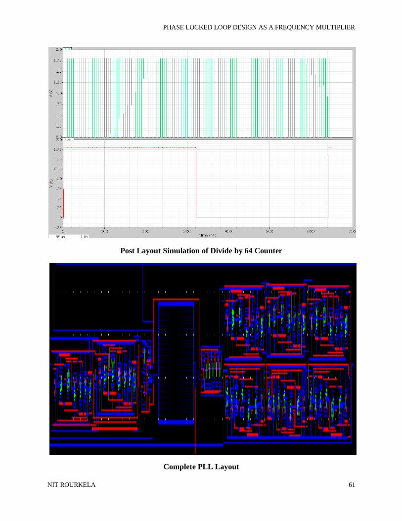
5.4 Divide by Counter
We design the VCO in such a way that the output of VCO is ‗N‘ times the reference
frequency. So the output o the VCO is passed through a divide by ‗N‘ counter and feedback
to the input. Here the D Flip-flop‘s QBAR is connected to the D input. It will work as a T
flip-flop with input connected to logic ‗1‘.The figure 45 shows the schematic of a divide by
64 counter.
Figure 45.Schematic of Divide by 64 Counter
Figure 46.Simulation of Divide by 64 Counter

PHASE LOCKED LOOP DESIGN AS A FREQUENCY MULTIPLIER
NIT ROURKELA 46
5.5 Phase Locked Loop
The phase frequency detector (comparator) produces an error output signal based on the
phase difference between the phase of the feedback clock and the phase of the reference clock.
Over time, small frequency differences accumulate as an increasing phase error. The difference
or error signal is low-pass filtered and drives the voltage controlled oscillator. The filtered error
signal acts as a control signal (Voltage or current) of the oscillator and adjusts the frequency of
oscillation to align feedback with
ref .The frequency of oscillation is divided down to the
feedback clock by a frequency divider. The phase is locked when the feedback clock has a
constant phase error and the same frequency as the reference clock. Because the feedback clock
is a divided version of the oscillator‘s clock frequency, the frequency of oscillation is N times the
reference clock.
Figure 47.Phase Locked Loop Schematic

PHASE LOCKED LOOP DESIGN AS A FREQUENCY MULTIPLIER
NIT ROURKELA 47
Figure 48.Simulation of 8.8 MHz
Figure 49.Simulation of 11.5 MHz

PHASE LOCKED LOOP DESIGN AS A FREQUENCY MULTIPLIER
NIT ROURKELA 48
CHAPTER 6
APPLICATIONS OF PLL &
CONCLUSIONS

PHASE LOCKED LOOP DESIGN AS A FREQUENCY MULTIPLIER
NIT ROURKELA 49
Phase-locked loops are widely used for synchronization purposes; in space communications
for coherent carrier tracking and threshold extension, bi synchronization, and symbol
synchronization. Phase-locked loops can also be used to demodulate frequency-modulated
signals. In radio transmitters, a PLL is used to synthesize new frequencies which are a
multiple of a reference frequency, with the same stability as the reference frequency.
6.1 Clock Recovery
Some data streams, especially high-speed serial data streams (such as the raw stream of data
from the magnetic head of a disk drive), are sent without an accompanying clock. The receiver
generates a clock from an approximate frequency reference, and then phase-aligns to the
transitions in the data stream with a PLL. This process is referred to as clock recovery. In order
for this scheme to work, the data stream must have a transition frequently enough to correct any
drift in the PLL's oscillator.
6.2 Clock Generation
Many electronic systems include processors of various sorts that operate at hundreds of
megahertz. Typically, the clocks supplied to these processors come from clock generator PLLs,
which multiply a lower-frequency reference clock (usually 50 or 100 MHz) up to the operating
frequency of the processor. The multiplication factor can be quite large in cases where the
operating frequency is multiple gigahertz and the reference crystal is just tens or hundreds of
megahertz.
6.3 Frequency Synthesis
A frequency synthesizer is an electronic system for generating a range of frequencies from a
single fixed time base or oscillator. Frequency Synthesizer manufacturers include Analog
Devices, National Semiconductor and Texas Instruments. VCO manufacturers include Sirenza,
Z-Communications.

PHASE LOCKED LOOP DESIGN AS A FREQUENCY MULTIPLIER
NIT ROURKELA 50
6.4 Conclusions
Phase Locked Loop is designed for a frequency multiplying factor of 64 and
verified.
The layouts of all the five blocks are drawn, extracted each block, performed the
post layout simulation and finally cross check with the functionality of the
schematic simulation.
A new high speed low glitch CMOS PFD is proposed. In the charge pump
configuration, a new current source is replaced.
In order to achieve the stability in the loop filter, a resistor is added in series with
the loop filter capacitor. Since the charge pump drives the series combination of
R1 and C1, each time a current is injected into the loop filter, the control voltage
experience a large jump. To relax this issue, a second capacitor is added in
parallel with R1 and C1.
Current starved VCO is selected as the voltage controlled oscillator in the design
of PLL.
A divide by 64 counters is used for the synchronization with the input frequency.
640 MHz is used in CMOS continuous-time sigma delta ADC, which can be
achieved with this PLL design.

PHASE LOCKED LOOP DESIGN AS A FREQUENCY MULTIPLIER
NIT ROURKELA 51
REFERENCES
1. Haripriya janardhan, MSEE Mahmud Fawzy Wagdy , ―Design of a 1GHz Digital
PLL Using 0.18μm CMOS Technology‖, IEEE International conference 2006.
2. H.O. Johansson, ―A Simple precharged CMOS Phase Frequency Detector‖, IEEE
Journal of Solid State Circuits, Volume 33, no 2, pp 295-299, Feb 1998.
3. Behzad Razavi, ―Design of Analog CMOS Integrated Circuits‖, Tata McGraw-
Hill Edition, 2002.
4. Hwang-Cherg Chow, Nan-Liang Yeh, ―A Lock-in Enhanced Phase Locked Loop
with High Speed Phase Frequency Detector‖, Proceedings to the International
Symposium on Intelligent Signal Processing and Communication Systems 2005,
Dec 13-16, Hong Kong.
5. G.B.Lee, P.K.Chan and L.Siek, ―A CMOS Phase Frequency Detector for Charge
Pump Phase Locked Loop‖, 42nd
Midwest Symposium on Circuits and Systems,
Aug 8-11, 1999, volume 2, Page 601-604.
6. Yubtzuan Chen, Hong-Yu Huang, ―A Fast Acquisition CMOS Phase Frequency
Detector‖, IEEE International Conference on Electro/Information Technology,
May 7-10, 2006, Page 488-491.
7. Yubtzuan Chen, Chih Ho Tu, Jein WI, ―A CMOS Phase Frequency Detector with
A High Speed Low Power D Type Master Slave Flip-flop‖, 45th Midwest
Symposium on Circuits and Systems, Aug 4-7, 2002, Volume 3, Page 389-392.
8. Milicevic S, Mac Eachern L, ―A Phase Frequency Detector and A Charge Pump
Design For PLL Applications‖, IEEE International Symposium on Circuits and
Systems 2008, May 18-21, Pages 1532-1535.
9. R.E.Best, "Phase-Locked Loops: Design, Simulation, and Applications‖, 3rd
edition, New York: McGraw-Hill, 1997.
10. Jan.M.Rabaey, Anantha Chandrakasan, Borivoje Nikolic, ―Digital Integrated
Circuits A design Perspective‖, Pearson education, 5th Indian Reprint 2005.

PHASE LOCKED LOOP DESIGN AS A FREQUENCY MULTIPLIER
NIT ROURKELA 52
11. M. Morris Mano, Michael.D.Ciletti, ―Digital Design‖, Prentice Hall, 4th edition,
2006.
12. B. Razavi, ―Monolithic Phase-Locked Loops and Clock Recovery Circuits”, IEEE
Press, 2003.
13. Johns, David A , Martin, Ken. ―Analog Integrated Circuit Design‖, John Wiley &
Sons, Inc, 1997.
14. D.H. Wolaver, ―Phase Locked Loop Circuit Design ―, Prentice Hall, 1991.
15. Woogeun Rhee, ―Design of High Performance CMOS Charge Pumps in Phase
Locked Loops‖, IEEE International Symposium on Circuits and Systems, pp 545-
548, May 1999.
16. L.Young et al, ― A PLL Clock Generator with 5 to 110 MHz of lock range for
microprocessors‖, IEEE Journal on Solid State Circuits, vol 38, no 8, pp 1028-
1038, Aug 2002.
17. W.-H. Lee, and J.-D. Cho, ―A High Speed and Low Power Phase-Frequency
Detector and Charge-Pump,‖ IEEE ASP-DAC '99. Asia and South Pacific, vol. 1,
pp. 269-272, 1999.
18. N. H. E. Weste and K. Eshragrian, ―Principles of CMOS VLSI Design,‖ 2nd ed.
Reading, MA Addison Wesley, 1993.
19. V. R. von Kaenel, "A High-speed, Low-Power Clock Generator for a
Microprocessor Application‖, IEEE journal of Solid- State Circuits. vol. 33, pp.
1634.1639, 1998.
20. R.C, Den Dulk, ―Digital PLL Lock Detection Circuit‖, Electronic Letters, Vol.
24, 880-882. 1988.
21. Cardner. F.M.: ―Charge-pump phase-lack loops‖, IEEE Transaction on
Communication, 1980, 28 pp, 1849-1858.
22. Brennan. P.V, ―Phase-locked loops, Principles and practice‖, McGraw-Hill 1996
23. M. V. Paemel, ―Analysis of a charge-pump PLL: a new model‖, IEEE
Transactions on Communication, vol. 42, pp. 2490-3498, July 1994.
24. I.-C. Hwang, S.-H. Song, and S.W. Kim, ―A digitally controlled phase-locked
loop with a digital phase-frequency detector for fast acquisition,‖ IEEE Journal of
Solid-State Circuits, vol. 36, pp. 1574- 1581, October. 2001.

PHASE LOCKED LOOP DESIGN AS A FREQUENCY MULTIPLIER
NIT ROURKELA 53
25. B. Razavi, Design of Integrated Circuits for Optical Communication, McGraw-
Hill, 1st ed. 2003, ch. 8.
26. J. Lee, M. Keel, S. Lim and S. Kim, ―Charge pump with perfect current matching
characteristics in phase-locked loops,‖ Electronics Letters, vol. 36, issue 23, pp.
1907-1908, Nov. 2000.
27. D. Armaroli, V. Liberali, and C. Vacchi, ―Behavioral analysis of charge pump
PLLs,‖ in Proc. Midwest Symp. Circuits Systems, Aug. 1995, pp. 893–896.
28. K.S. Lee, B.H. Park, H. Lee, and M. J. Yoh, ―Phase frequency detectors for fast
frequency acquisition in zero-dead-zone CPPLLs for mobile communication
systems.‖ ESSCIRC '03. Proceedings of the 29th European, pp. 525-528,
September 2003.
29. M. Soyuer, and R. G. Meyer, ―Frequency limitations of a conventional phase-
frequency detector,‖ IEEE Journal of Solid-State Circuits, vol. 25, pp. 1019-1022,
August 1990.
30. W.H. Lee and J.D. Cho, ―A High Speed and Low Power Phase- Frequency
Detector and Charge-Pump,‖ IEEE ASP-DAC‘99. Asia and South Pacific, vol. 1,
pp.269-272, 1999.
31. R. C. Chang, and L.C.Kuo, ―A differential type CMOS phase frequency
detector,‖ Proceedings of the Second IEEE Asia Pacific Conference on 28-30, pp.
61-64, August 2000.
32. M. Mansuri, D. Liu, and C.-K.K. Yang, ―Fast frequency acquisition phase-
frequency detectors for Gsamples/s phase-locked loops,‖ IEEE Journal of Solid-
State Circuits, vol. 37, pp. 1375 - 1382 November 2002.

PHASE LOCKED LOOP DESIGN AS A FREQUENCY MULTIPLIER
NIT ROURKELA 54
LAYOUTS
Layout of Low Glitch High Speed CMOS PFD
Av_Extracted view of Low Glitch High Speed CMOS PFD

PHASE LOCKED LOOP DESIGN AS A FREQUENCY MULTIPLIER
NIT ROURKELA 55
Post Layout Simulation of Low Glitch High Speed CMOS PFD
Layout of the Charge Pump

PHASE LOCKED LOOP DESIGN AS A FREQUENCY MULTIPLIER
NIT ROURKELA 56
Av_extracted view of the Charge Pump
Layout of 13.57nf Capacitor

PHASE LOCKED LOOP DESIGN AS A FREQUENCY MULTIPLIER
NIT ROURKELA 57
Av_extracted view of 13.57nf Capacitor
Layout of 2.71nf Capacitor

PHASE LOCKED LOOP DESIGN AS A FREQUENCY MULTIPLIER
NIT ROURKELA 58
Av_extracted view of 2.71nf Capacitor
Layout of resistor

PHASE LOCKED LOOP DESIGN AS A FREQUENCY MULTIPLIER
NIT ROURKELA 59
Layout of Voltage Controlled Oscillator
Av_extracted view of Voltage Controlled Oscillator

PHASE LOCKED LOOP DESIGN AS A FREQUENCY MULTIPLIER
NIT ROURKELA 60
Layout of Divide by 64 Counter
Av_extracted view of Divide by 64 Counter
PHASE LOCKED LOOP DESIGN AS A FREQUENCY MULTIPLIER
NIT ROURKELA 61
Post Layout Simulation of Divide by 64 Counter
Complete PLL Layout