Thermal Physics in Electronic and Optoelectronic Materials ...
Upload
zuleika-inaraCategory
view
62download
4description
Mech 473 LectureElectronic & Photonic Materials
Professor Rodney Herring
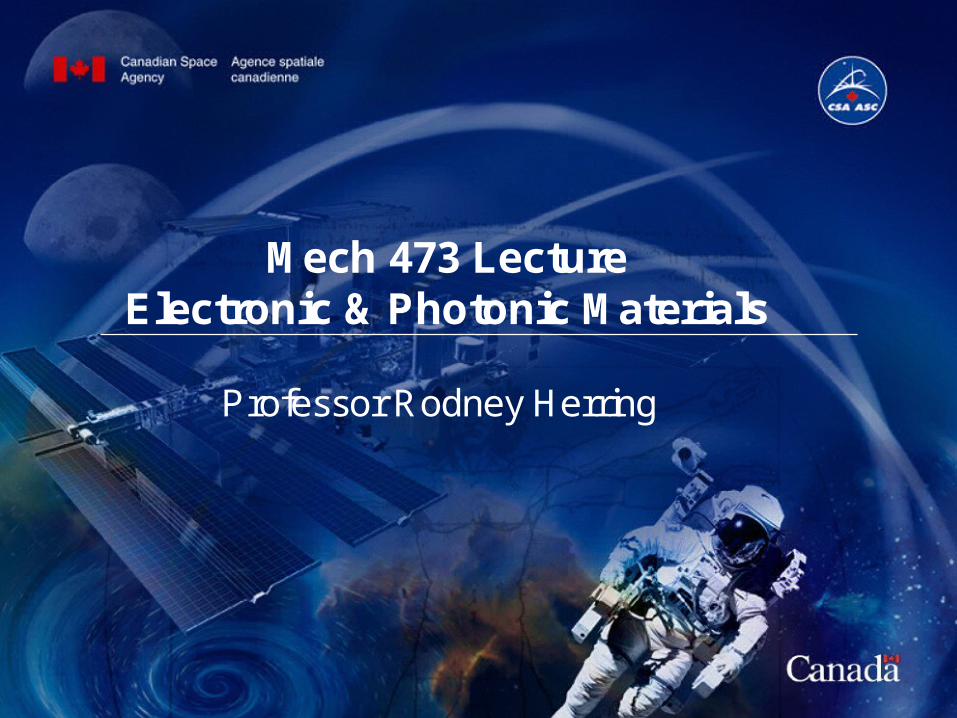
• This image has been simulated using CCDs located on the helmet to detect the surroundings and flexible LEDs located in the clothing and elsewhere to re-emit the light of the surroundings in an advanced camouflage device.
• Project supported by DARPA (defense advanced research project agency) of DoD.
Optoelectronic Materials

Charge Couple Devices
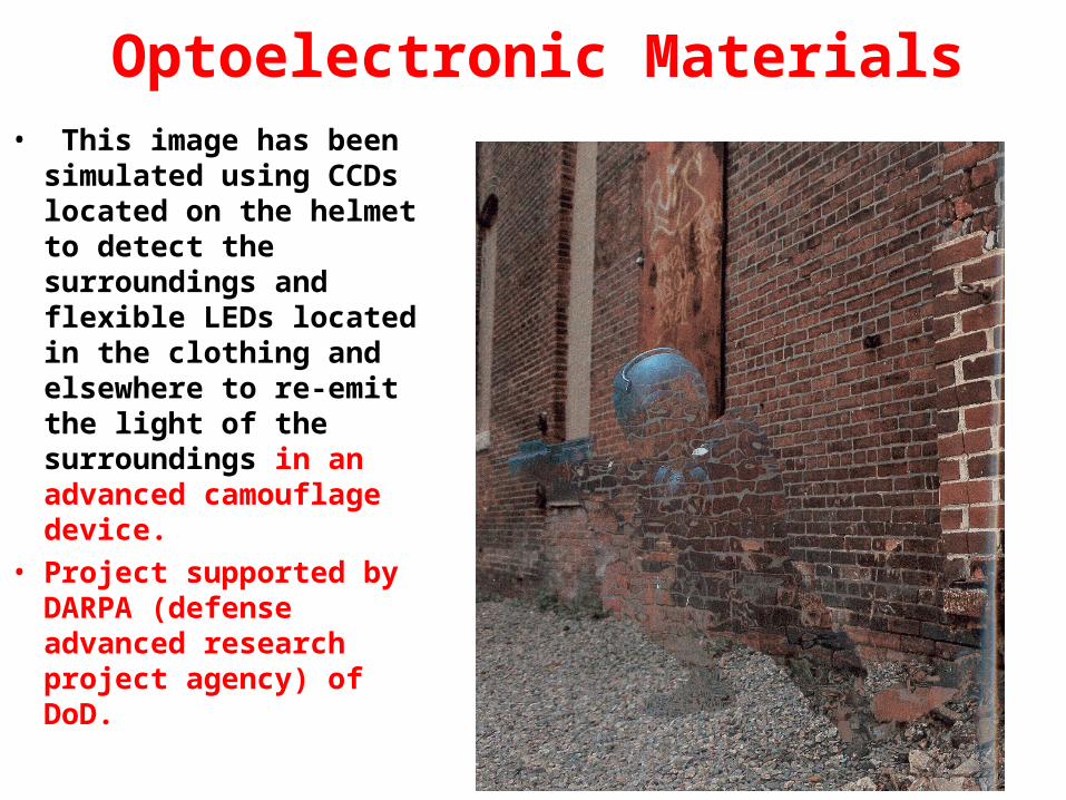
• Charge Couple Devices, or CCDs are made up of an array of metal-oxide-semiconductor (MOS) capacitors, i.e., a composite.
• Small pixel size of the CCD ~5 m, with a provision for optical input, make the device suitable for high-density imaging.
• CCDs are used for almost all digital imaging devices today.
Charge Couple Devices
A CCD shown as an array of MOS capacitors
Charge Couple Devices• CCDs rely upon the charge generation in the depletion region
of the MOS capacitor.
• An applied voltage, which is pulsed, holds the charge created by the photons generating current in the photodiode.
• The potential in the capacitor is linearly dependent on the voltage applied to the surface electrode.
• The charges are confined laterally, since the neighbouring MOS capacitor is at a lower potential, so the charges do not leave the potential well.
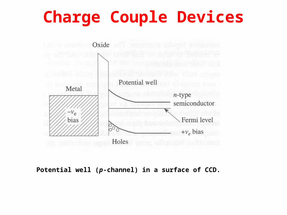
Charge Couple Devices
Potential well (p-channel) in a surface of CCD.
Charge Couple Devices• The amount of charge generated depends on the light intensity
and the period during which light is allowed to fall on the CCD.
• The charges are then shifted out serially from the array using a shift registry.
• The stored charges in the pulses mutually repel each other, although thermal diffusion and self-induced drift can blur individual pulses.
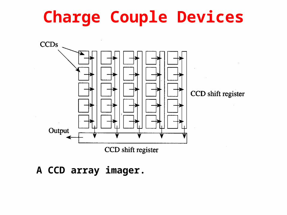
Charge Couple Devices
A CCD array imager.
Charge Couple Devices
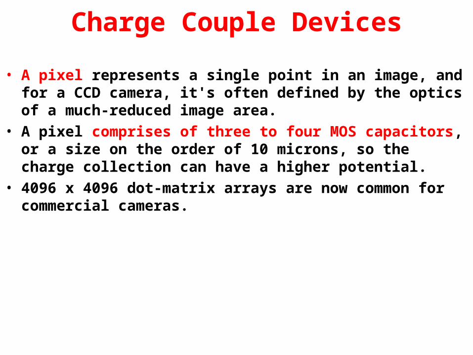
• A pixel represents a single point in an image, and for a CCD camera, it's often defined by the optics of a much-reduced image area.
• A pixel comprises of three to four MOS capacitors, or a size on the order of 10 microns, so the charge collection can have a higher potential.
• 4096 x 4096 dot-matrix arrays are now common for commercial cameras.
Charge Couple Devices
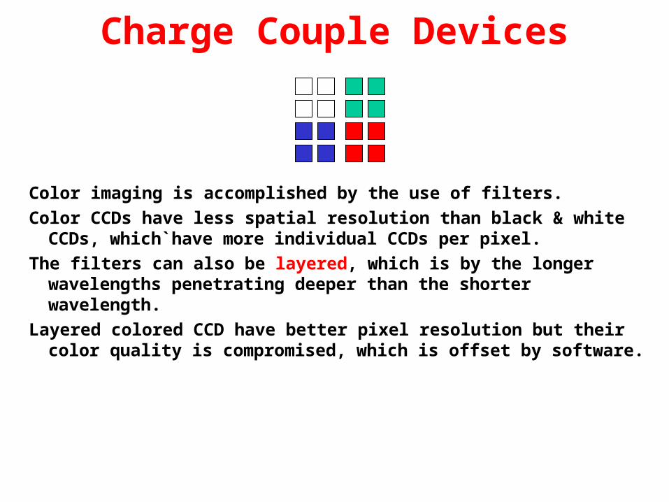
Color imaging is accomplished by the use of filters.
Color CCDs have less spatial resolution than black & white CCDs, which`have more individual CCDs per pixel.
The filters can also be layered, which is by the longer wavelengths penetrating deeper than the shorter wavelength.
Layered colored CCD have better pixel resolution but their color quality is compromised, which is offset by software.
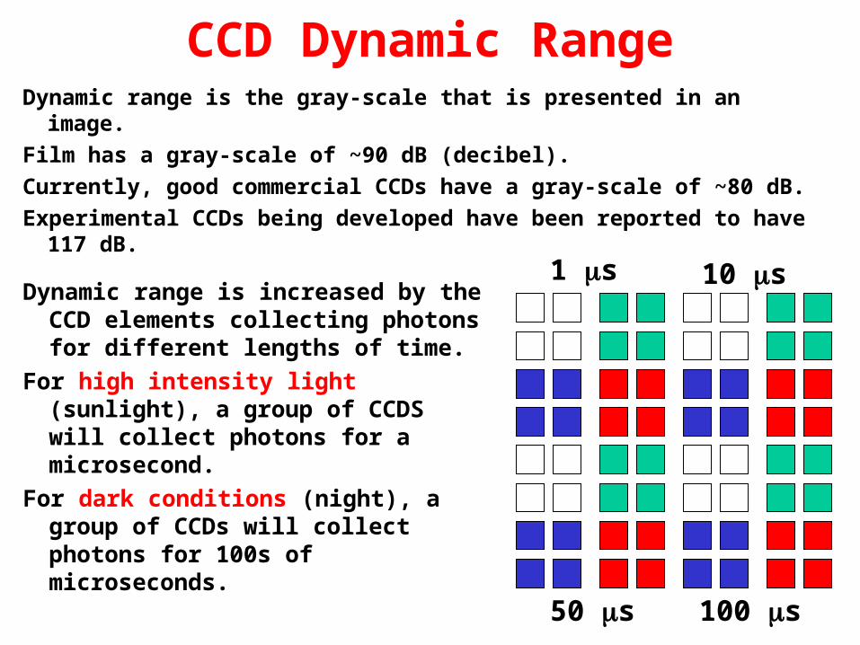
CCD Dynamic RangeDynamic range is the gray-scale that is presented in an image.
Film has a gray-scale of ~90 dB (decibel).
Currently, good commercial CCDs have a gray-scale of ~80 dB.
Experimental CCDs being developed have been reported to have 117 dB.
Dynamic range is increased by the CCD elements collecting photons for different lengths of time.
For high intensity light (sunlight), a group of CCDS will collect photons for a microsecond.
For dark conditions (night), a group of CCDs will collect photons for 100s of microseconds.
1 s 10 s
50 s 100 s
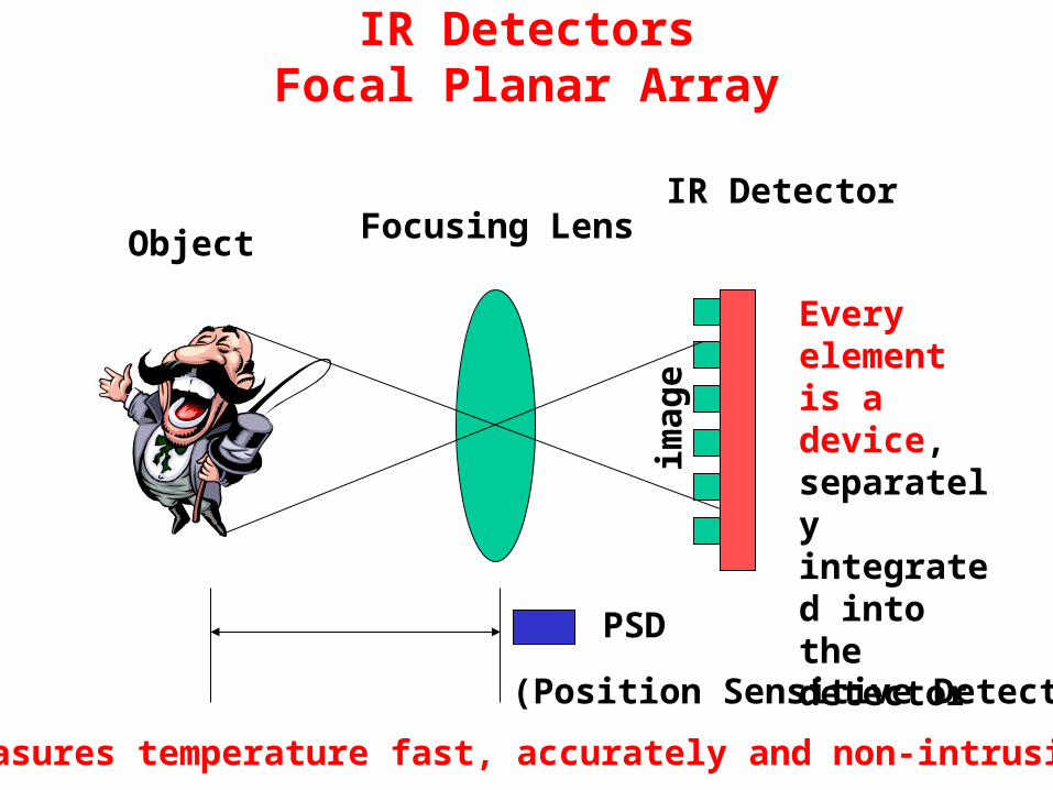
IR DetectorsFocal Planar Array
Object Focusing LensIR Detector
Every element is a device, separately integrated into the detector
PSD
(Position Sensitive Detector)im
age
Measures temperature fast, accurately and non-intrusively.
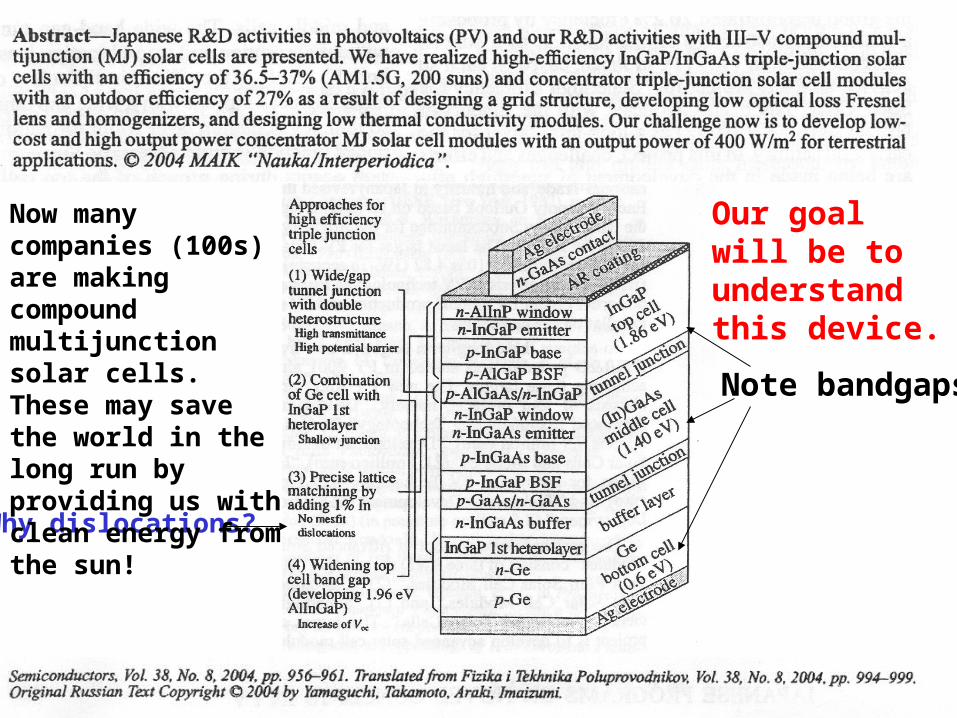
Note bandgaps
Why dislocations?
Now many companies (100s) are making compound multijunction solar cells.These may save the world in the long run by providing us with clean energy from the sun!
Our goal will be to understand this device.
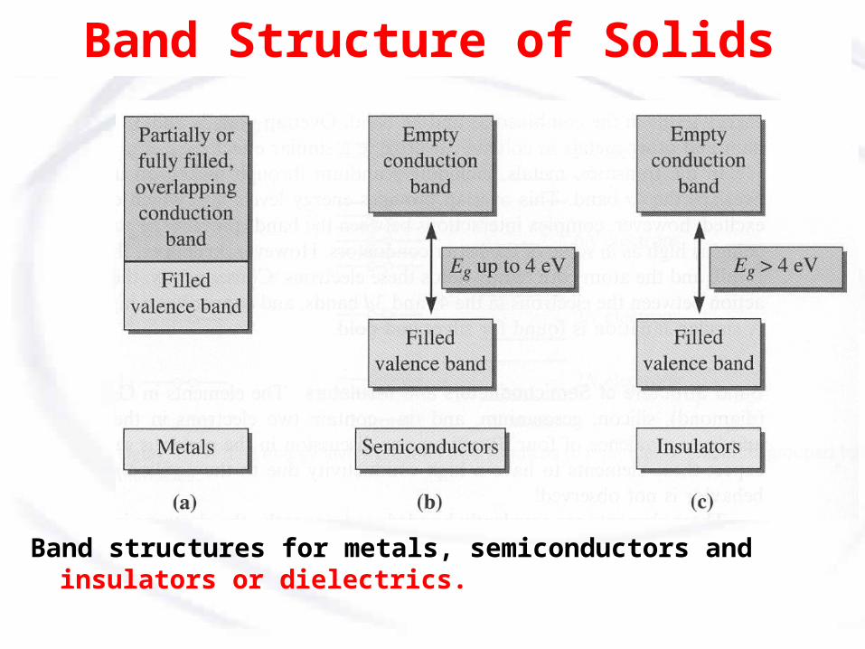
Band Structure of Solids
Band structures for metals, semiconductors and insulators or dielectrics.
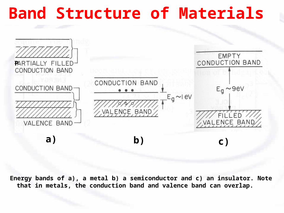
Band Structure of Materials
Energy bands of a), a metal b) a semiconductor and c) an insulator. Note that in metals, the conduction band and valence band can overlap.
a) b) c)
P
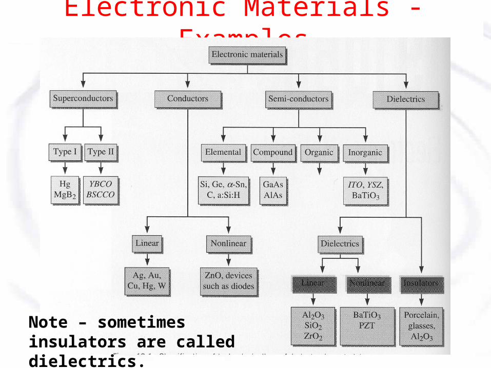
Electronic Materials - Examples
Note – sometimes insulators are called dielectrics.
Intrinsic/ Extrinsic SemiconductorsAn intrinsic semiconductor is one who properties are not controlled by impurities or
dopants. An example would be pure Silicon.
An extrinsic semiconductor (n or p type) is preferred for devices since its properties are temperature stable and can be controlled using ion implantation or diffusion of dopants. An example would be doped Si.
Since the energy gap between the valence and conduction bands in semiconductors is relatively small, some electrons possess enough thermal energy to exceed the gap and enter the conduction band.
The excited electrons leave behind unoccupied energy levels or holes in the valence band.
When an electron moves to fill a hole, another hole is created from the original electron source. The holes appear to act as positive charged electrons carrying an electric charge.
Conductivity of Intrinsic Semiconductors
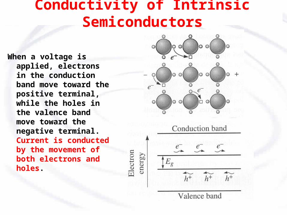
When a voltage is applied, electrons in the conduction band move toward the positive terminal, while the holes in the valence band move toward the negative terminal. Current is conducted by the movement of both electrons and holes.
Conductivity of Intrinsic Semiconductors
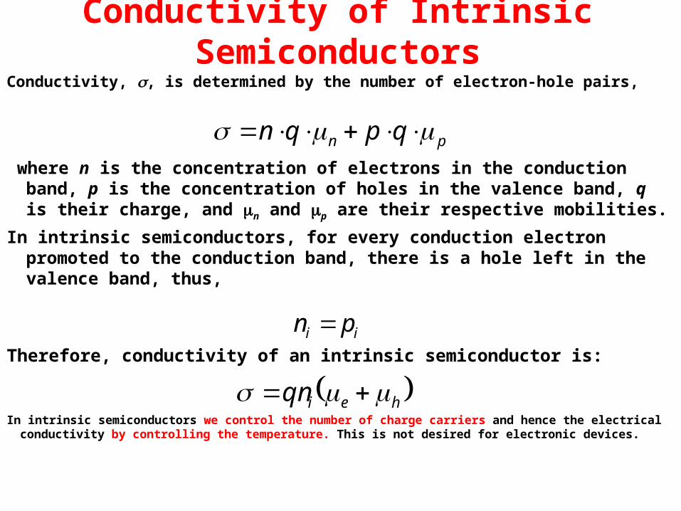
Conductivity, , is determined by the number of electron-hole pairs,
where n is the concentration of electrons in the conduction band, p is the concentration of holes in the valence band, q is their charge, and n and p are their respective mobilities.
In intrinsic semiconductors, for every conduction electron promoted to the conduction band, there is a hole left in the valence band, thus,
pn qpqn
ii pn Therefore, conductivity of an intrinsic semiconductor is:
heiqn In intrinsic semiconductors we control the number of charge carriers and hence the electrical conductivity by
controlling the temperature. This is not desired for electronic devices.
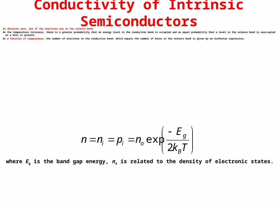
Conductivity of Intrinsic SemiconductorsAt absolute zero, all of the electrons are in the valence band.
As the temperature increases, there is a greater probability that an energy level in the conduction band is occupied and an equal probability that a level in the valence band is unoccupied or a hole is present.
As a function of temperature, the number of electrons in the conduction band, which equals the number of holes in the valence band is given by an Arrhenius expression,
Tk
Enpnn
B
goii 2
exp
where Eg is the band gap energy, no is related to the density of electronic states.
Conductivity of Intrinsic Semiconductors
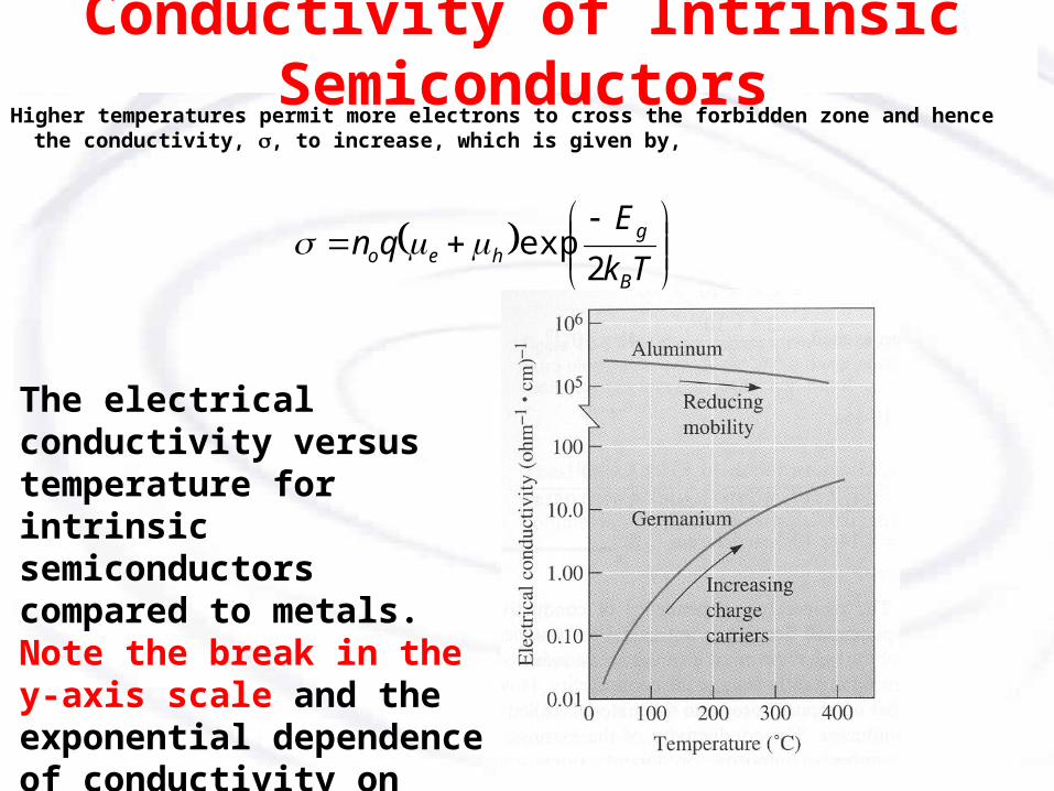
Higher temperatures permit more electrons to cross the forbidden zone and hence the conductivity, , to increase, which is given by,
Tk
Eqn
B
gheo 2
exp
The electrical conductivity versus temperature for intrinsic semiconductors compared to metals. Note the break in the y-axis scale and the exponential dependence of conductivity on temperature.
Electronic Properties of Semiconductors
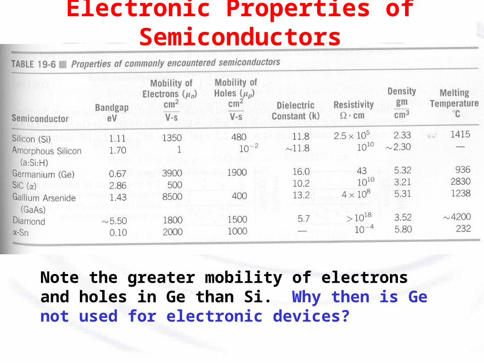
Note the greater mobility of electrons and holes in Ge than Si. Why then is Ge not used for electronic devices?
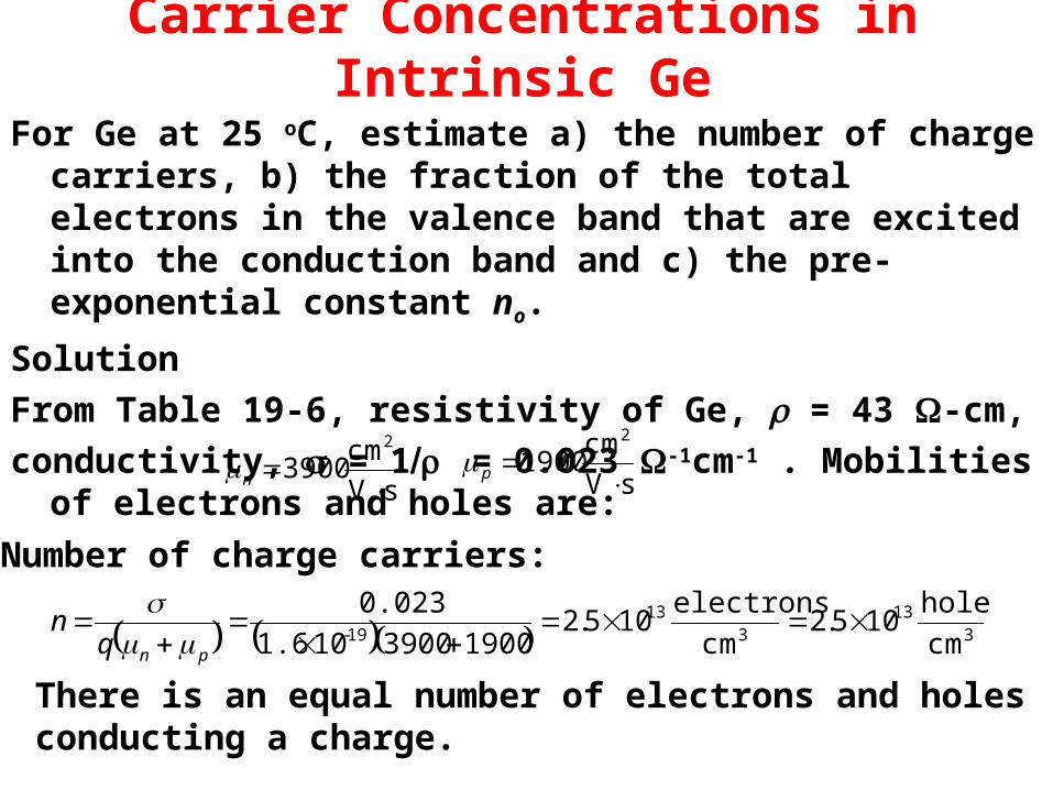
Carrier Concentrations in Intrinsic Ge
For Ge at 25 oC, estimate a) the number of charge carriers, b) the fraction of the total electrons in the valence band that are excited into the conduction band and c) the pre-exponential constant no.
Solution
From Table 19-6, resistivity of Ge, = 43 -cm,
conductivity, = 1 = 0.023 -1cm-1 . Mobilities of electrons and holes are:
sV
cm 3900
2
n
sV
cm 1900
2
p
a) Number of charge carriers:
313
313
19- cm
holes 105.2
cm
electrons 105.2
19003900101.6
0.023
pnqn
There is an equal number of electrons and holes conducting a charge.
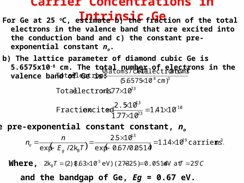
Carrier Concentrations in Intrinsic GeFor Ge at 25 oC, estimate b) the fraction of the total electrons in the
valence band that are excited into the conduction band and c) the constant pre-exponential constant no.
b) The lattice parameter of diamond cubic Ge is 5.6575x10⁻⁸ cm. The total number of electrons in the valence band of Ge is:
38 cm) 106575.5(
atomselectrons/ 4atoms/cell 8electrons Total
231077.1electrons Total
1023
13
1041.11077.1
102.5 excitedFraction
c) the pre-exponential constant constant, no
319
13
B
mcarriers/c 1014.10514.0/67.0exp
105.2
2k/exp
TE
nn
go
CTT o25at eV 0.051425)eV)(273 1063.8)(2(k2 5B Where,
and the bandgap of Ge, Eg = 0.67 eV.
Conductivity of Extrinsic Semiconductors
The temperature dependence of conductivity in intrinsic semiconductors is exponential but this is not useful for practical applications.
For intrinsic semiconductors, slight changes in temperature significantly change the conductivity.
By intentionally adding a small number of impurity atoms to the material called doping, we can produce an extrinsic semiconductor.
The conductivity of extrinsic semiconductors depends primarily on the number of impurity, or dopant, atoms and in a certain temperature range is independent of temperature.
Thus extrinsic semiconductors can be “tuned” by dopants for device applications.
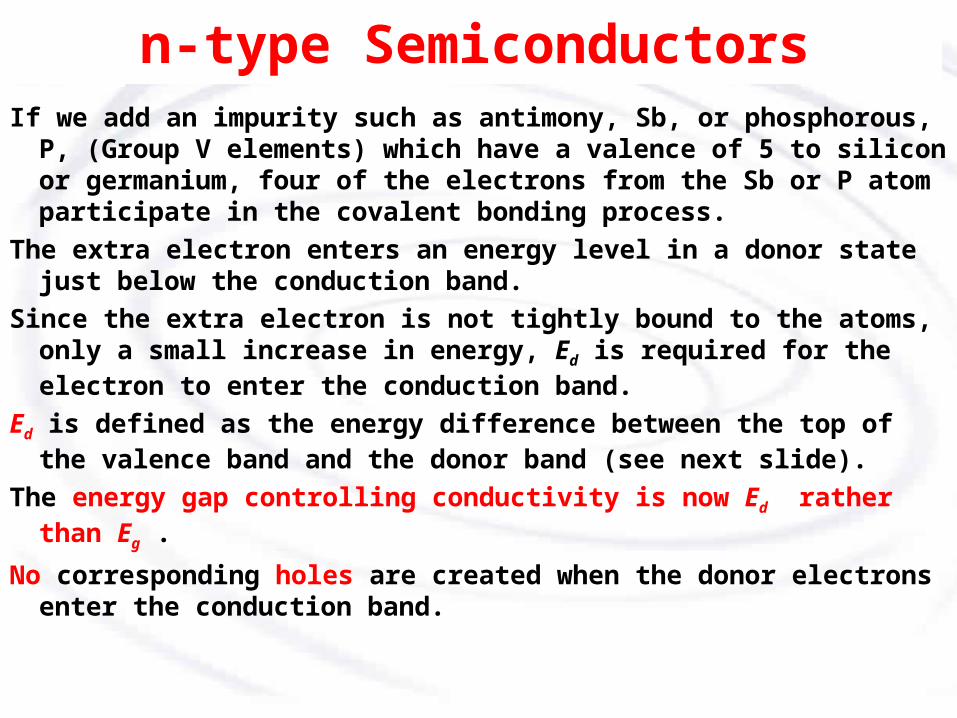
n-type SemiconductorsIf we add an impurity such as antimony, Sb, or phosphorous, P, (Group
V elements) which have a valence of 5 to silicon or germanium, four of the electrons from the Sb or P atom participate in the covalent bonding process.
The extra electron enters an energy level in a donor state just below the conduction band.
Since the extra electron is not tightly bound to the atoms, only a small increase in energy, Ed is required for the electron to enter the conduction band.
Ed is defined as the energy difference between the top of the valence band and the donor band (see next slide).
The energy gap controlling conductivity is now Ed rather than Eg .
No corresponding holes are created when the donor electrons enter the conduction band.
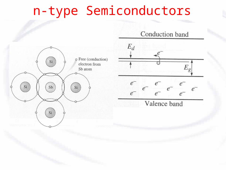
n-type Semiconductors
p-type SemiconductorsWhen we add an impurity such as gallium or boron (Group III in
the Periodic Table), which have a valence of three, to Si or Ge, there are not enough electrons to complete the covalent bonding process.
An electron hole is created in the valence band.
The holes act as acceptors of electrons.
It can be filled by electrons from the other locations in the band.
These holes sites have a somewhat higher than normal energy and create an acceptor level of possible electron energies just above the valence band.
An electron must gain an energy of only Ea in order to create a hole in the valence band.
The hole then moves and carries the charge.
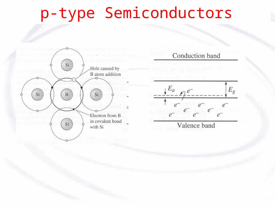
p-type Semiconductors
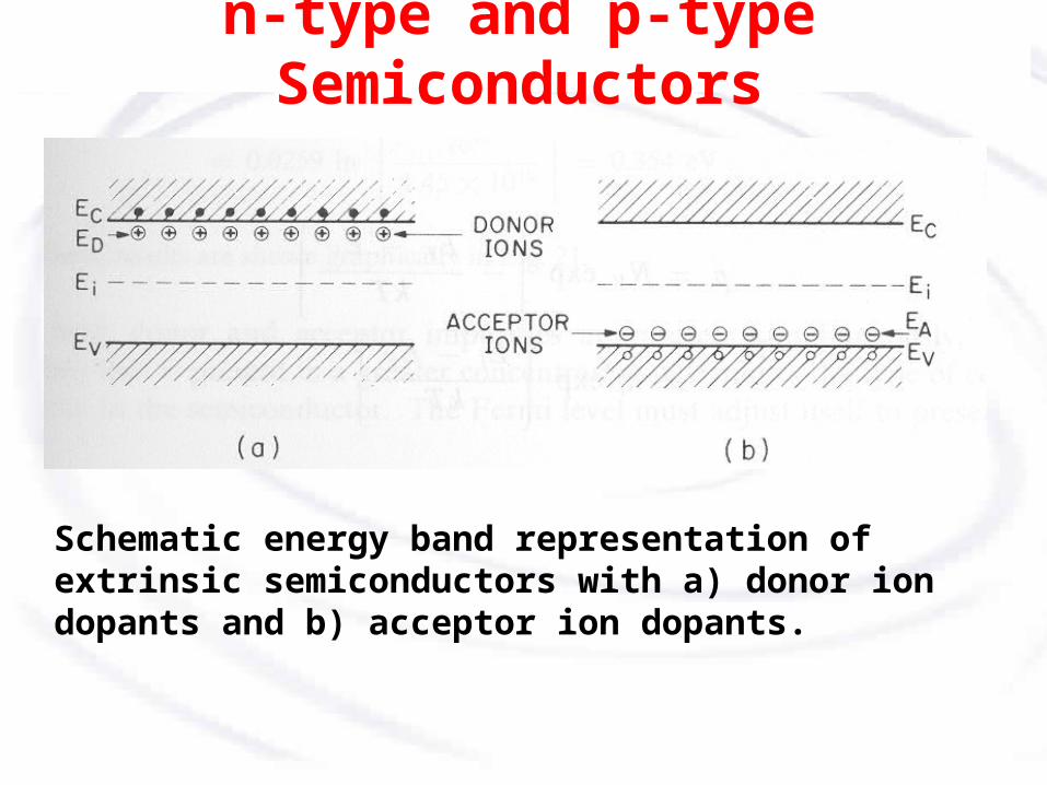
n-type and p-type Semiconductors
Schematic energy band representation of extrinsic semiconductors with a) donor ion dopants and b) acceptor ion dopants.
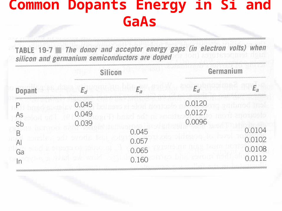
Common Dopants Energy in Si and GaAs
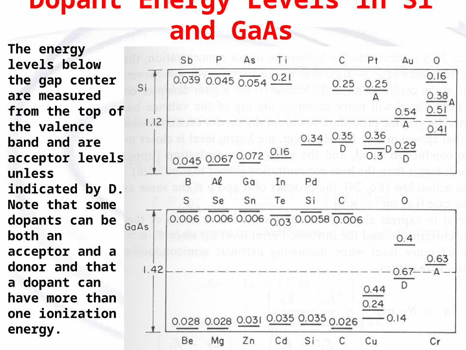
Dopant Energy Levels in Si and GaAsThe energy levels below the gap center are measured from the top of the valence band and are acceptor levels unless indicated by D.Note that some dopants can be both an acceptor and a donor and that a dopant can have more than one ionization energy.
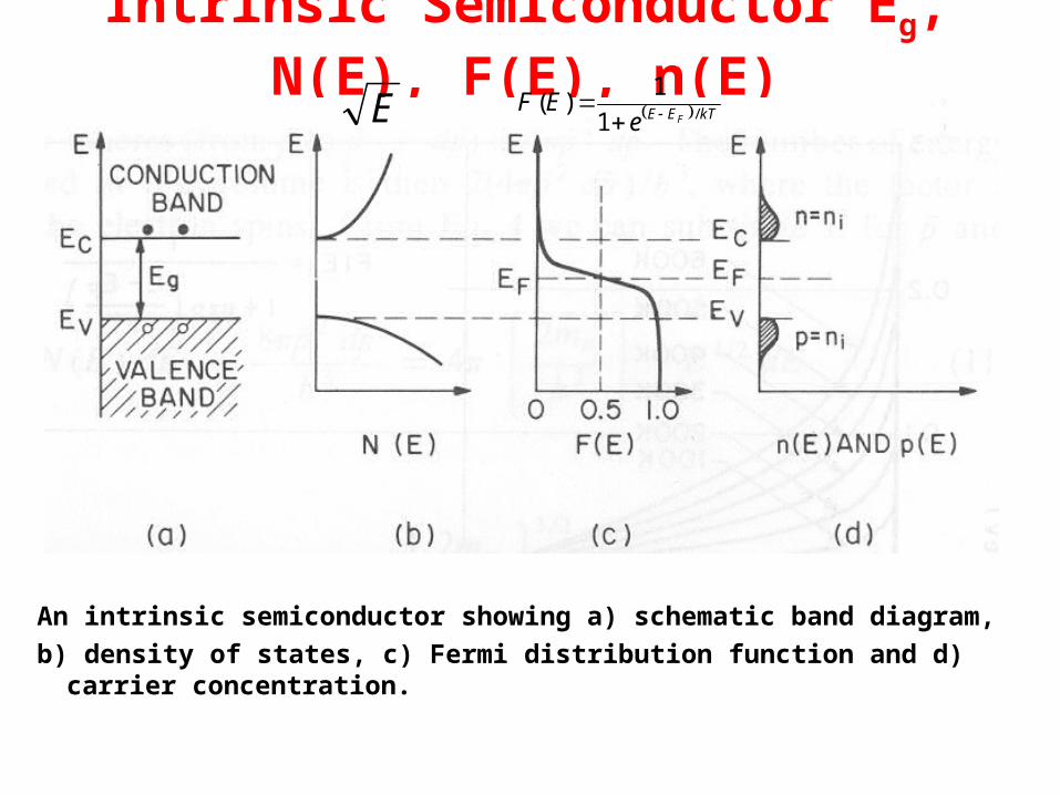
Intrinsic Semiconductor Eg, N(E), F(E), n(E)
An intrinsic semiconductor showing a) schematic band diagram,
b) density of states, c) Fermi distribution function and d) carrier concentration.
E kTEE FeEF /1
1)(
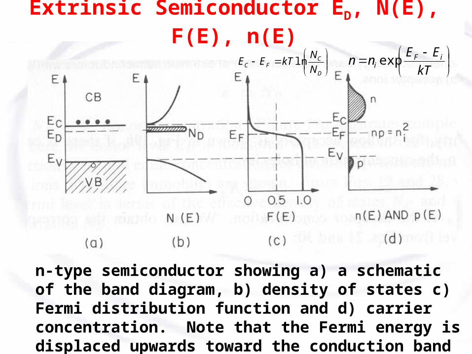
Extrinsic Semiconductor ED, N(E), F(E), n(E)
n-type semiconductor showing a) a schematic of the band diagram, b) density of states c) Fermi distribution function and d) carrier concentration. Note that the Fermi energy is displaced upwards toward the conduction band for n-type semiconductors.
D
CFC N
NkTEE ln
kT
EEnn iFi exp
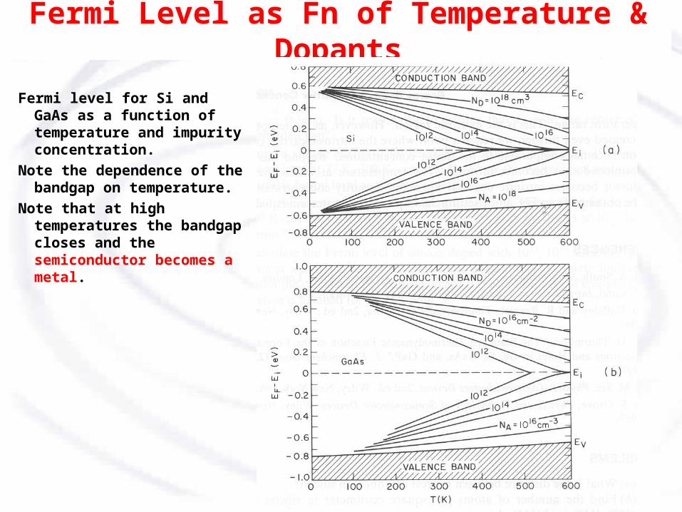
Fermi Level as Fn of Temperature & Dopants
Fermi level for Si and GaAs as a function of temperature and impurity concentration.
Note the dependence of the bandgap on temperature.
Note that at high temperatures the bandgap closes and the semiconductor becomes a metal.
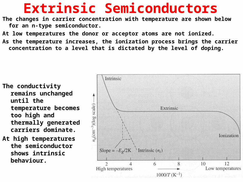
Extrinsic SemiconductorsThe changes in carrier concentration with temperature are shown below for an n-
type semiconductor.
At low temperatures the donor or acceptor atoms are not ionized.
As the temperature increases, the ionization process brings the carrier concentration to a level that is dictated by the level of doping.
The conductivity remains unchanged until the temperature becomes too high and thermally generated carriers dominate.
At high temperatures the semiconductor shows intrinsic behaviour.
Photonic MaterialsPhotonic materials have had a significant impact on the development
of the communications infrastructure and information technology.
Photonic materials have also played a key role in many other technologies related to medicine, manufacturing, astronomy, etc.
The term optoelectronics refers to the science and technology that combines electronic and optical materials.
Examples would include light emitting diodes (LEDs), solar cells and semiconductor lasers.
Optical properties of materials are related to the interaction of a material with electromagnetic radiation in the form of waves or particles of energy called photons.
The optical properties of materials involve their emission of photons and the interaction of photons with the materials.
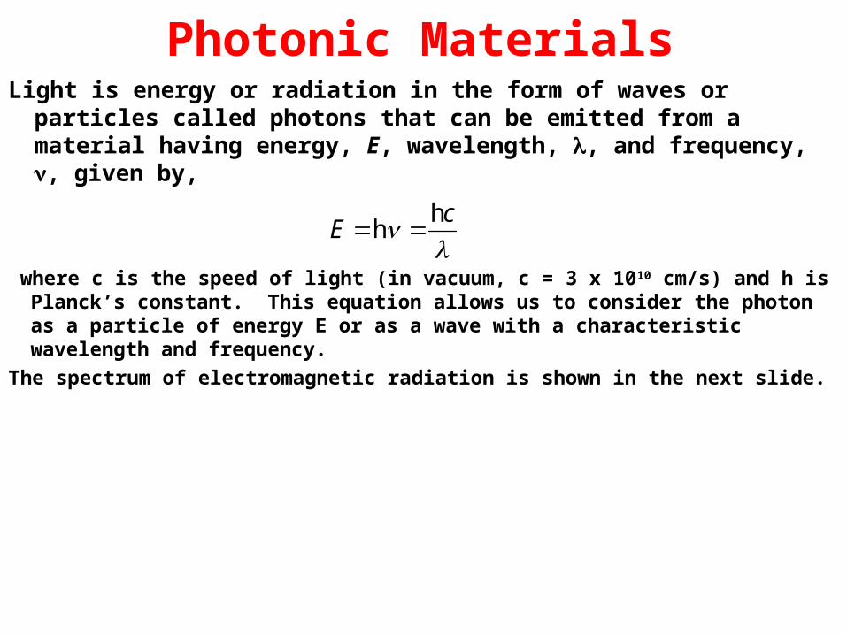
Photonic MaterialsLight is energy or radiation in the form of waves or particles called
photons that can be emitted from a material having energy, E, wavelength, , and frequency, , given by,
c
Eh
h
where c is the speed of light (in vacuum, c = 3 x 1010 cm/s) and h is Planck’s constant. This equation allows us to consider the photon as a particle of energy E or as a wave with a characteristic wavelength and frequency.
The spectrum of electromagnetic radiation is shown in the next slide.
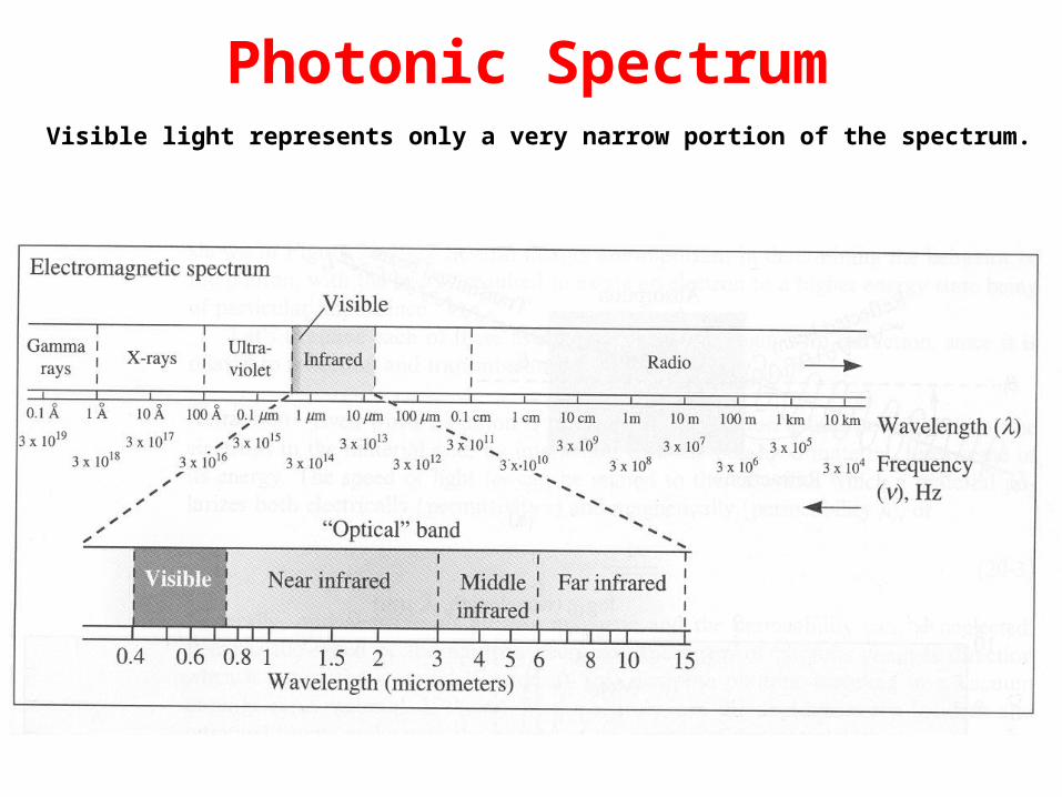
Visible light represents only a very narrow portion of the spectrum.
Photonic Spectrum
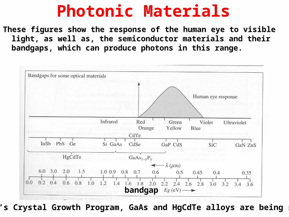
These figures show the response of the human eye to visible light, as well as, the semiconductor materials and their bandgaps, which can produce photons in this range.
Photonic Materials
bandgap
In UVic’s Crystal Growth Program, GaAs and HgCdTe alloys are being studied.
Photon-Material Interactions
All materials interact in some way with light.If the photon interacts with the valence electrons by giving up its energy, absorption occurs. This is desired for optical detectors.If the photon gives up its energy but photons of identical energy are re-emitted by the material then reflection occurs.If the photon does not interact with the electronic structure of the material then transmission occurs.If transmission occurs then the velocity of the photon is altered and refraction occurs.If an electron falls from a high energy state to a low energy state then a photon can be created and emission occurs.
Photon-Material Interactions
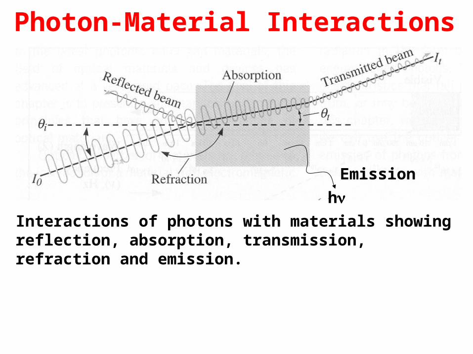
Interactions of photons with materials showing reflection, absorption, transmission, refraction and emission.
Emission
h
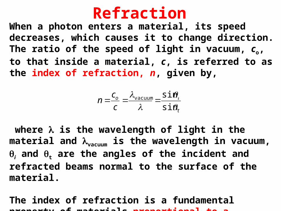
RefractionWhen a photon enters a material, its speed decreases, which causes it to change direction.The ratio of the speed of light in vacuum, co, to that inside a material, c, is referred to as the index of refraction, n, given by,
t
o
c
cn
sin
sinvacuum
where is the wavelength of light in the material and vacuum is the wavelength in vacuum, i and t are the angles of the incident and refracted beams normal to the surface of the material.
The index of refraction is a fundamental property of materials proportional to a materials composition and temperature.
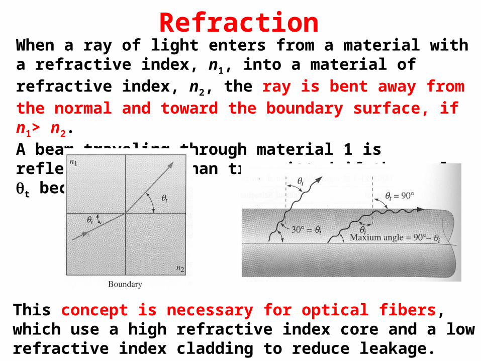
RefractionWhen a ray of light enters from a material with a refractive index, n1, into a material of refractive index, n2, the ray is bent away from the normal and toward the boundary surface, if n1> n2.A beam traveling through material 1 is reflected rather than transmitted if the angle t becomes 90o.
This concept is necessary for optical fibers, which use a high refractive index core and a low refractive index cladding to reduce leakage.
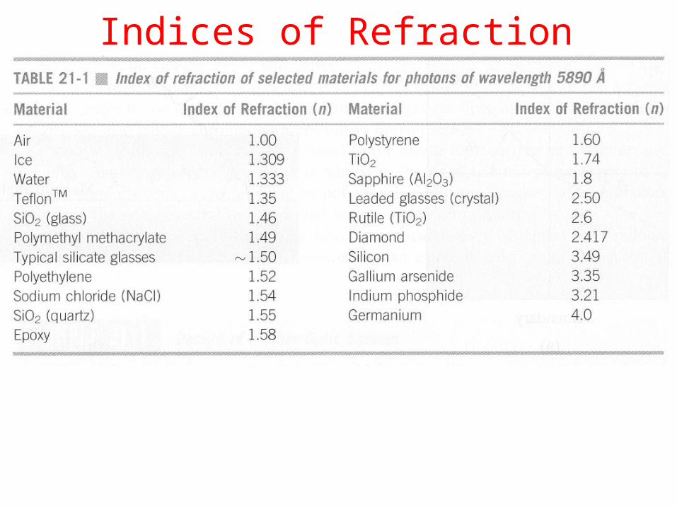
Indices of Refraction
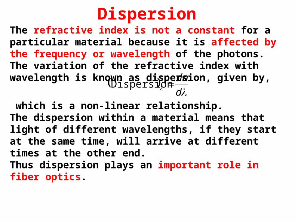
DispersionThe refractive index is not a constant for a particular material because it is affected by the frequency or wavelength of the photons.The variation of the refractive index with wavelength is known as dispersion, given by,
d
dnDispersion
which is a non-linear relationship.The dispersion within a material means that light of different wavelengths, if they start at the same time, will arrive at different times at the other end.Thus dispersion plays an important role in fiber optics.
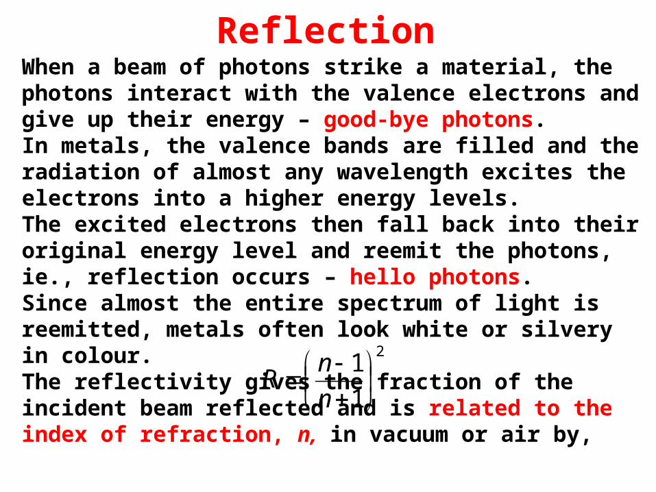
ReflectionWhen a beam of photons strike a material, the photons interact with the valence electrons and give up their energy – good-bye photons.In metals, the valence bands are filled and the radiation of almost any wavelength excites the electrons into a higher energy levels.The excited electrons then fall back into their original energy level and reemit the photons, ie., reflection occurs – hello photons.Since almost the entire spectrum of light is reemitted, metals often look white or silvery in colour.The reflectivity gives the fraction of the incident beam reflected and is related to the index of refraction, n, in vacuum or air by,
2
1
1
n
nR
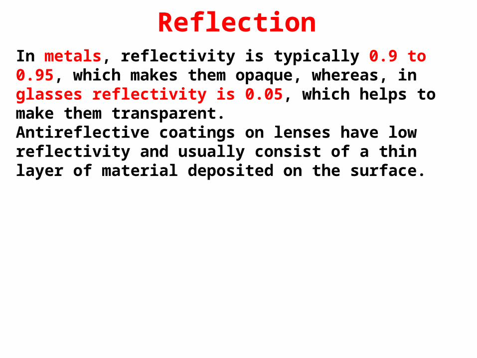
ReflectionIn metals, reflectivity is typically 0.9 to 0.95, which makes them opaque, whereas, in glasses reflectivity is 0.05, which helps to make them transparent.Antireflective coatings on lenses have low reflectivity and usually consist of a thin layer of material deposited on the surface.
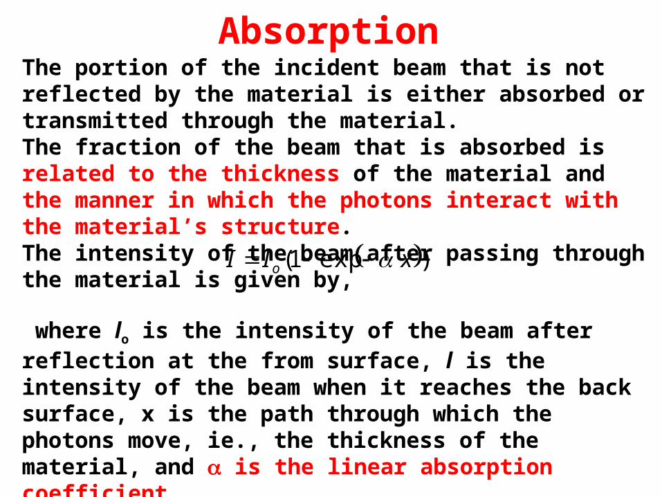
AbsorptionThe portion of the incident beam that is not reflected by the material is either absorbed or transmitted through the material.The fraction of the beam that is absorbed is related to the thickness of the material and the manner in which the photons interact with the material’s structure.The intensity of the beam after passing through the material is given by,
) exp1( xII o
where lo is the intensity of the beam after reflection at the from surface, l is the intensity of the beam when it reaches the back surface, x is the path through which the photons move, ie., the thickness of the material, and is the linear absorption coefficient.
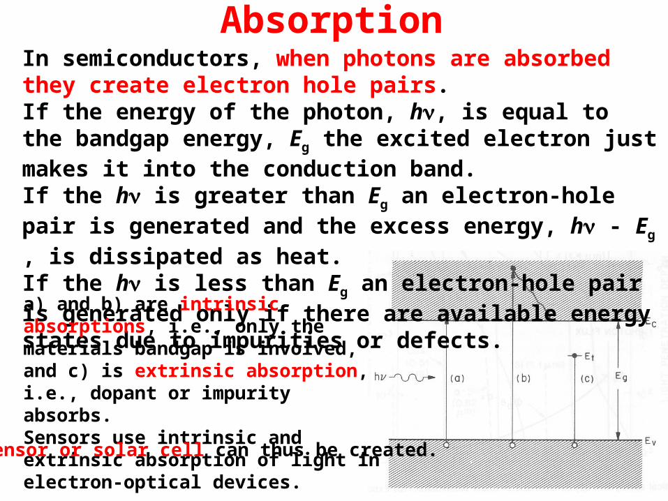
AbsorptionIn semiconductors, when photons are absorbed they create electron hole pairs.If the energy of the photon, h, is equal to the bandgap energy, Eg the excited electron just makes it into the conduction band.If the h is greater than Eg an electron-hole pair is generated and the excess energy, h - Eg , is dissipated as heat.If the h is less than Eg an electron-hole pair is generated only if there are available energy states due to impurities or defects.
a) and b) are intrinsic absorptions, i.e., only the materials bandgap is involved, and c) is extrinsic absorption, i.e., dopant or impurity absorbs.Sensors use intrinsic and extrinsic absorption of light in electron-optical devices.
A sensor or solar cell can thus be created.
Absorption
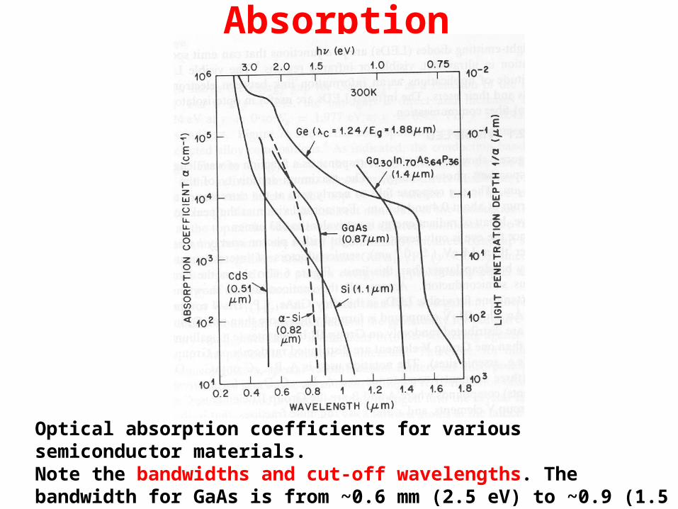
Optical absorption coefficients for various semiconductor materials.Note the bandwidths and cut-off wavelengths. The bandwidth for GaAs is from ~0.6 mm (2.5 eV) to ~0.9 (1.5 eV).
Emission
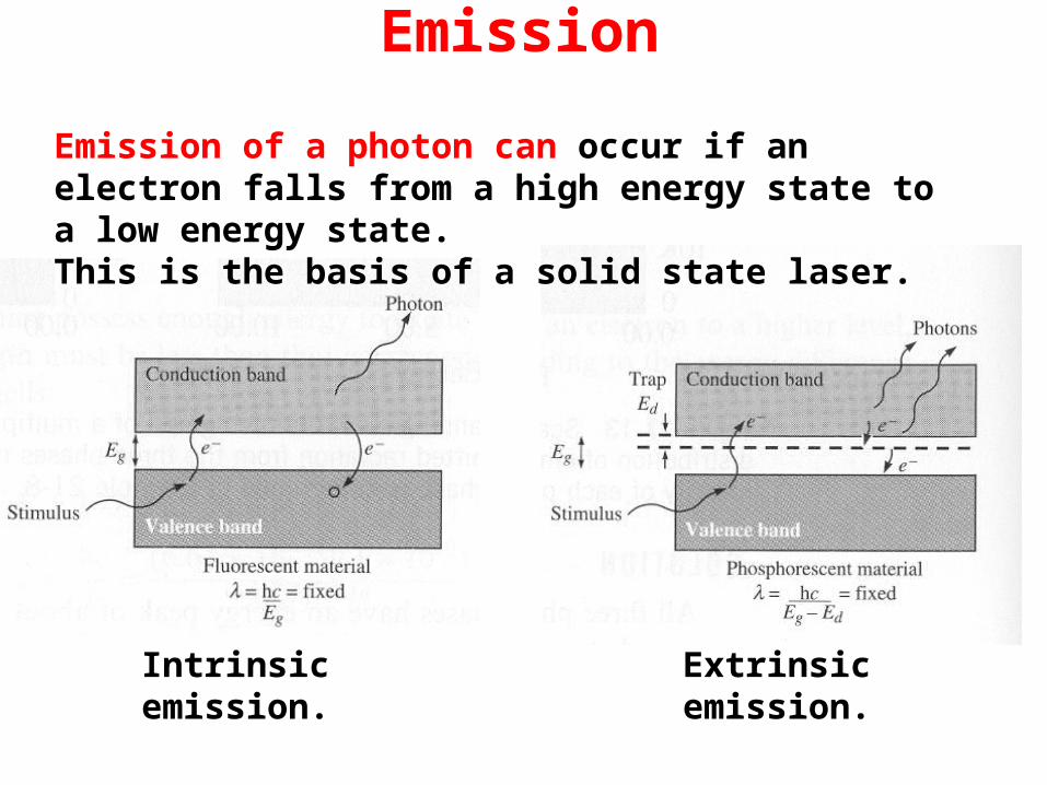
Intrinsic emission. Extrinsic emission.
Emission of a photon can occur if an electron falls from a high energy state to a low energy state. This is the basis of a solid state laser.
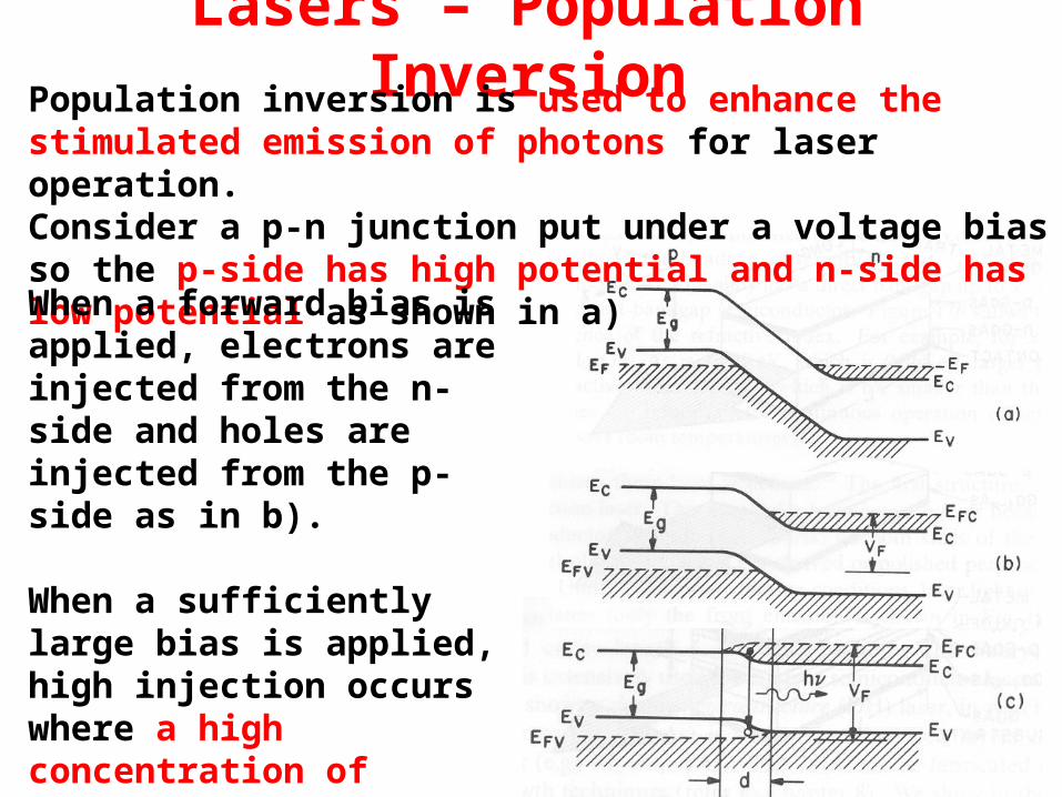
Lasers – Population InversionPopulation inversion is used to enhance the stimulated emission of photons for laser operation.Consider a p-n junction put under a voltage bias so the p-side has high potential and n-side has low potential as shown in a)
When a forward bias is applied, electrons are injected from the n-side and holes are injected from the p-side as in b).
When a sufficiently large bias is applied, high injection occurs where a high concentration of electrons and holes can recombine to produce photons as in c).
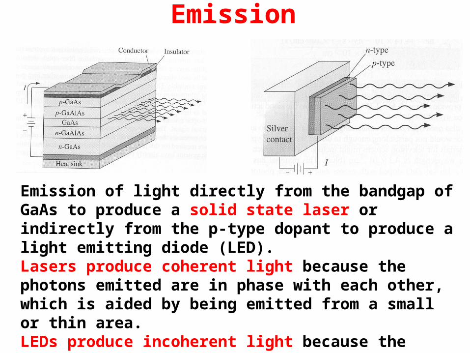
Emission
Emission of light directly from the bandgap of GaAs to produce a solid state laser or indirectly from the p-type dopant to produce a light emitting diode (LED).Lasers produce coherent light because the photons emitted are in phase with each other, which is aided by being emitted from a small or thin area.LEDs produce incoherent light because the photons being emitted are out of phase with each other, having been emitted from a large area?
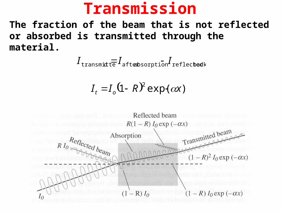
TransmissionThe fraction of the beam that is not reflected or absorbed is transmitted through the material.
back reflectedabsorptionafter dtransmitte III
)exp(1 2 xRII ot
Transmission• Due to absorption, there exists a “window” in which transmission occurs for materials, which is determined by the bandgap (Eg) of the material and the energy of the incoming photon.• The following slide summarizes the conditions for transmission and absorption.
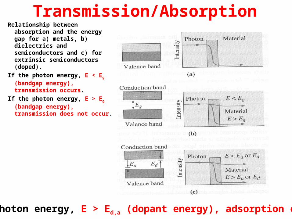
Transmission/AbsorptionRelationship between absorption
and the energy gap for a) metals, b) dielectrics and semiconductors and c) for extrinsic semiconductors (doped).
If the photon energy, E < Eg
(bandgap energy), transmission occurs.
If the photon energy, E > Eg
(bandgap energy), transmission does not occur.
If the photon energy, E > Ed,a (dopant energy), adsorption can occur.
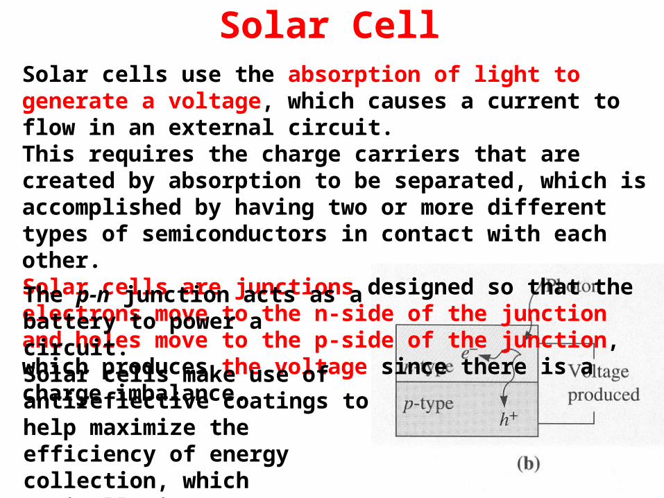
Solar CellSolar cells use the absorption of light to generate a voltage, which causes a current to flow in an external circuit.This requires the charge carriers that are created by absorption to be separated, which is accomplished by having two or more different types of semiconductors in contact with each other.Solar cells are junctions designed so that the electrons move to the n-side of the junction and holes move to the p-side of the junction, which produces the voltage since there is a charge imbalance.
The p-n junction acts as a battery to power a circuit.Solar cells make use of antireflective coatings to help maximize the efficiency of energy collection, which typically is ~10 to 20%, although recent developments are better than 30% efficient.
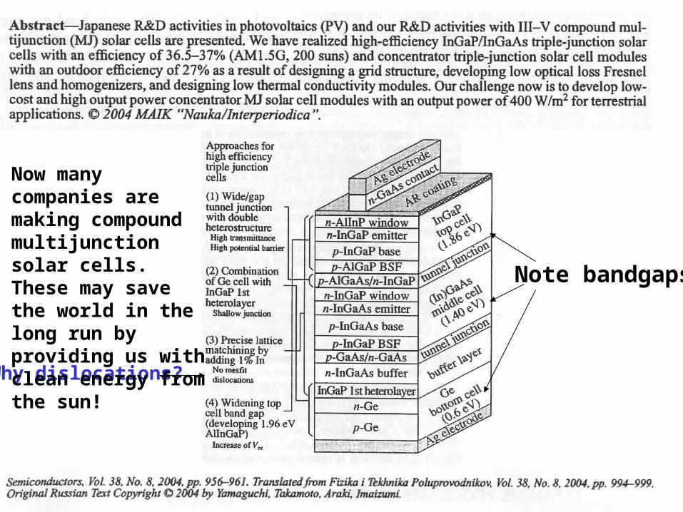
Note bandgaps
Why dislocations?
Now many companies are making compound multijunction solar cells.These may save the world in the long run by providing us with clean energy from the sun!

The End(Any questions or comments?)