Thermal Physics in Electronic and Optoelectronic Materials ...
149
Thermal Physics in Electronic and Optoelectronic Materials and Devices by Abhishek Yadav A dissertation submitted in partial fulfillment of the requirements for the degree of Doctor of Philosophy (Mechanical Engineering) in The University of Michigan 2010 Dissertation Committee: Assistant Professor Kevin P. Pipe, Co-Chair Assistant Professor Max Shtein, Co-Chair Associate Professor Rachel S. Goldman Associate Professor Katsuo Kurabayashi
Transcript of Thermal Physics in Electronic and Optoelectronic Materials ...
Thermal Physics in Electronic and Optoelectronic Materials and
Devices
by
Abhishek Yadav
A dissertation submitted in partial fulfillment of the requirements for the degree of
Doctor of Philosophy (Mechanical Engineering)
in The University of Michigan 2010
Dissertation Committee:
Assistant Professor Kevin P. Pipe, Co-Chair Assistant Professor Max Shtein, Co-Chair Associate Professor Rachel S. Goldman Associate Professor Katsuo Kurabayashi
© Abhishek Yadav 2010
All Rights Reserved
ii
Acknowledgements
First and foremost, I would like to thank my advisors Prof. Kevin P. Pipe and Prof. Max
Shtein. Their advice, motivation, and, ideas have been instrumental for this work. Prof.
Kevin Pipe was a continuous source of new and innovative ideas. His objectivity and
persistence were always helpful when facing challenging research problems. Prof. Max
Shtein helped me through infinite discussions we had during our group meetings. His
knowledge in organic semiconductors was helpful in bringing my research to quick
fruition. His passion towards research and commitment for excellence always inspired
me.
I am also grateful to my committee members Prof. Rachel S. Goldman and Prof. Katsuo
Kurabayashi. Prof. Rachel Goldman provided many critical comments for work on
quantum dot superlattices, which led to a better understanding of underlying issues.
Being a GSI with Prof. Kurabayashi was helpful in understanding the importance of
teaching in academia.
This work would not have been possible without help from many colleagues and
collaborators including: Paddy Chan, Kwang Hyup An, Huarui Sun, Brendan O’Connor,
Yiying Zhao, Steven E. Morris, Yansha Jin, Gunho Kim, Andrea Bianchini, Denis
Nothern, Jinjjing Li and Chelsea Haughn. Paddy Chan and Huarui Sun sat next to my
desk for most of my stay here, and, shared many meals and ideas about science. Paddy

iii
Chan introduced me to the field of thermoreflectance, which was the starting point of my
work on temperature modulation spectroscopy. Huarui Sun discussed intricate details of
my research, and provided many useful ideas. Kwang Hyup An trained me on thermal
evaporation system and many other experimental setups. Yansha Jin trained with me on
TEM and shared many useful ideas about electron microscopy. Steve Morris helped me
with thermal evaporation and purification of organic material.
I am also grateful to many friends who made my stay at Ann Arbor fun including:
Deepak Kumar, Krispian Lawrence, Kulwinder Singh and Manvendu Bharadwaj.
Deepak’s advice on all matters of life was helpful.
Finally, this work would not have been possible without the support of my parents
Satyanarain and Nisha Yadav and my sister Sugandha Yadav, who have shared my joys
throughout past 5+ years.
iv
Table of Contents Acknowledgements……………………………………………………………………… ii
List of Figures…………………………………………………………………………….viii
List of Tables………………………………………………………………………….. xv
Chapter 1 1
Introduction……………………………………………………………………………….. 1
1.1 Thermal effects on electronic and transport properties of semiconductors ......... 1
1.1.1 How does temperature affect the electronic bandgap? ................................. 1
1.1.2 How does temperature affect the Fermi distribution? ................................... 2
1.1.3 How does temperature affect the scattering of free carriers? ....................... 4
1.1.4 How does temperature affect scattering of phonons? ................................... 5
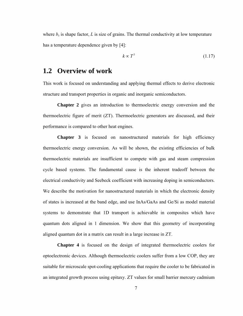
1.2 Overview of work ................................................................................................. 7
Chapter 2 10
Thermoelectric energy conversion……………………………………………………… 10
2.1 Thermoelectric transport .................................................................................... 10
2.2 Thermoelectric devices ...................................................................................... 11
2.2.1 Thermoelectric power generator ................................................................. 11
where Z is the dimensionless thermoelectric figure of merit defined by: 13
2.2.2 Thermoelectric cooler ................................................................................. 14
v
2.3 Status of thermoelectric materials ...................................................................... 16
Chapter 3 18
Thermoelectric properties of aligned quantum dot chains……………………………… 18
3.1 Theory of thermoelectric transport ..................................................................... 18
3.2 Nanostructured materials for high efficiency thermoelectric devices ................ 22
3.3 Theory and Calculation Method ......................................................................... 26
3.4 Single Quantum Dot Chains: Size Effects ......................................................... 29
3.5 QD Chain Nanocomposite ................................................................................. 31
3.6 Comparison of QD chains with 3D ordered QD nanocomposites ..................... 36
3.7 Summary and Conclusions ................................................................................. 40
Chapter 4 42
Integrated Thermoelectric Coolers for Mercury Cadmium Telluride Based Infrared
Detectors………………………………………………………………………………… 42
4.1 Introduction ........................................................................................................ 42
4.2 Cross-plane Seebeck coefficient and thermal conductivity of small-barrier Hg1-
xCdxTe superlattices ...................................................................................................... 43
4.2.1 Measurement of Seebeck coefficient and thermal conductivity of thin films
44
4.2.2 Results and discussion ................................................................................ 49
4.3 Design of integrated thermoelectric cooler ........................................................ 51
4.3.1 Design considerations ................................................................................. 51
4.3.2 Coupled electrothermal modeling ............................................................... 52
4.3.3 Results and discussion ................................................................................ 54
4.4 Summary and conclusions .................................................................................. 56
vi
Chapter 5 58
Fiber-based flexible thermoelectric power generator………………………………….. 58
5.1 Introduction ........................................................................................................ 58
5.2 Materials and processes for flexible thermoelectric devices .............................. 60
5.3 Single-fiber thermoelectric power generators .................................................... 63
5.3.1 Fabrication method and testing procedure .................................................. 63
5.3.2 Measurement of thermoelectric power generation characteristics .............. 64
5.3.3 Optimization of material parameters for maximizing power generation .... 67
5.4 Multi-fiber thermoelectric power generators: Plain weave geometry ............... 72
5.4.1 Fabrication method and testing procedure .................................................. 73
5.4.2 Results and discussion ................................................................................ 76
5.5 Summary ............................................................................................................ 80
Chapter 6 82
Organic photovoltaics 82
6.1.1 Materials and device structures ................................................................... 83
6.1.2 Working principle of organics photovoltaics .............................................. 85
6.2 Summary ............................................................................................................ 89
Chapter 7 90
Temperature Modulation Spectroscopy for Studying Excitonic Properties of Organic
Semiconductors…………………………………………………………………………..90
7.1 Introduction ........................................................................................................ 90
7.2 Determining the nature of excitonic transitions ................................................. 94
7.2.1 Electric field modulation spectroscopy ....................................................... 95
7.2.2 Piezomodulation spectroscopy .................................................................... 97
vii
7.3 Temperature modulation spectroscopy .............................................................. 98
7.3.1 Theory ......................................................................................................... 98
7.3.2 Experimental setup.................................................................................... 100
7.4 Results and Discussion ..................................................................................... 104
7.4.1 Morphology of CuPc films ....................................................................... 104
7.4.2 Optical spectrum and data fitting .............................................................. 107
7.4.3 Temperature modulation spectrum ........................................................... 110
7.5 Summary and Conclusions ............................................................................... 118
Chapter 8 120
Conclusions……………………………………………………………………………. 120
8.1 Summary of present work ................................................................................ 120
8.2 Suggestions for future work ............................................................................. 122
8.2.1 Effect of band bending on thermoelectric power factor of metal
nanoparticle-semiconductor nanocomposites ......................................................... 122
8.2.2 Fabrication of thermoelectric materials on plastic substrates ................... 122
8.2.3 Stark effect imaging of organic field effect transistors ............................. 123
Bibliography…………………………………………………………………………… 124
viii
List of Figures
Figure 1.1. Effect of temperature on Fermi distribution………………………………….4
Figure 1.2 Thermal conductivity of GaAs as a function of temperature. Low temperature thermal conductivity is determined by boundary scattering, while, high temperature thermal conductivity is determined by phonon scattering……………………………….6
Figure 1.3. An overview of the work in this thesis……………………………………...9
Figure 2.1. Illustration of different thermoelectric effects (a) Seebeck effect (b) Peltier effect, and, (c) Thomson effect…………………………………………………………10
Figure 2.2. (a) Schematic of a thermoelectric power generator (b) picture of commercially available thermoelectric unit from Melcor……………………………….12
Figure 2.3. Maximum efficiency of thermoelectric power generator as a function of heat source temperature for different dimensionless figure of merit…………………………13
Figure 2.4. Schematic of a thermoelectric cooler with a solid state description of the origin of cooling…………………………………………………………………………15
Figure 2.5. Maximum COP of a thermoelectric refrigerator as a function of dimensionless figure of merit ZT for Th=300K and ΔT = 30K. The COP of commercially available, vapor compression cycle based refrigerators is also shown………………..…14
Figure 2.6. ZT of best thermoelectric materials as a function of temperature. From reference Tritt [4]………………………………………………………………………...17
Figure 3.1. (a) Density of states (b) Fermi distribution (c) derivative of Fermi function (d) electrical conductivity and (e) seebeck coefficient as a function of energy………….21
ix
Figure 3.2. Electronic density of states of 3D bulk material, 2D quantum well and 1D quantum nanowire………………..………………………………………………………23
Figure 3.3. (a) Thermoelectric power factor of bulk III-V semiconductors (b) Thermoelectric power factor of III-V semiconductor nanowires. Figures reproduced from Mingo…………………………………………………………………………………….24
Figure 3.4. Illustration of aligned quantum dot chain, energy minibands, and potential wells in x,y, and z directions. Lx, Ly and Lz are the QD sizes in x,y,z directions, Hx is QD spacing along direction of alignment, V0 is the confining potential, and Veff is the effective confining potential for the x direction……………………………………………………26
Fig. 3.5. (a) Electrical conductivity, (b) Seebeck coefficient, and (c) power factor as a function of Fermi level for individual InAs/GaAs QD chain with Lx=10nm and Hx=5nm. Triangles denote the maximum in S2σ of bulk and QD chain with dot size Ly=Lz=5nm, used in the calculation of normalized S2σ of the QD chain nanocomposite in Fig. 3………………………………………………………………………………….………31
Figure 3.6. Comparison of normalized power factors, (i.e. the maximum power factor divided by the maximum power factor of the bulk) for the QD chain nanocomposite and random QD nanocomposite. For the InAs/GaAs system, QD dimensions and spacing for 1D chain are Lx=10nm, Ly=Lz=5nm and Hx=5nm. For the Ge/Si QD system, QD dimensions and spacing are Lx=Ly=Lz=4nm and Hx=2nm. Lx,Ly,Lz are dot dimensions in x,y,z directions and Hx is dot spacing along the alignment direction…………………….32
Figure 3.7. The average interchain spacing (solid line) is plotted on left axis and miniband widths (dotted lines) and 4 times the scattering potential (dotted line) are plotted on right axis as a function of the QD volume fraction. (a) The first and second minibands widths are plotted for InAs/GaAs dot chains with size and spacing as in Fig. 3. (b) The first, second and third minibands widths are plotted for Ge/Si dot chains with size and spacing as in Fig. 3…………………………………………………………………..34
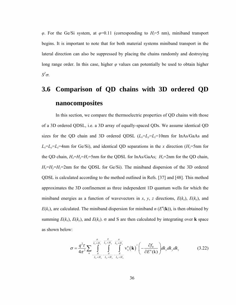
Figure 3.8. (a) Electrical conductivity, (b) Seebeck coefficient, and (c) power factor as a function of Fermi level for InAs/GaAs 1D QD chain with Lx= Ly= Lz=10nm and Hx=5nm, 3D QDSL with Lx= Ly= Lz=10nm and Hx= Hy= Hz=5nm, and bulk GaAs………..……..37
Figure 3.9. (a) Electrical conductivity, (b) Seebeck coefficient, and (c) power factor as a function of Fermi level for Ge/Si 1D QD chain with Lx= Ly= Lz=4nm and Hx=2nm, 3D
x
QDSL with Lx= Ly= Lz=4nm and Hx= Hy= Hz=2nm, and bulk Si………………….…….39
Figure 4.1. Setup for in plane Seebeck coefficient measurement……………………….41
Figure 4.2. Illustration of setup for cross plane Seebeck coefficient measurement……..45
Figure 4.3. Illustration of differential method for cross-plane Seebeck coefficient and thermal conductivity measurement…………………………………………...………….46
Figure 4.4. Schematic of SL structure used for measurement…………………………..47
Figure 4.5. Measurement setup………………………………………………………….48
Figure 4.6. (a) Thermoelectric voltage developed and (b) Temperature difference between top and bottom edge of mesa as a function of power applied to the heater…….49
Figure 4.7. Proposed geometry of an integrated thermoelectric cooler for cooling infrared detector pixels……………………………………………………………………………51
Figure 4.8. Breakdown of thermal resistances of different layers. Also shown are location of Peltier heating and cooling………………………………………….............52
Figure 4.9. (a) ANSYS drawing of cooler and detector pixel mesa (b) 3D meshing of all layers……………………………………………………………………………………..53
Figure 4.10. The average temperature drop on detector pixel surface. tsubstrate = 800μm and tbuffer = 8μm………………………………………………………………….……….54
Figure 4.11. (a) The average temperature drop on detector pixel surface. tsubstrate = 30 μm and tbuffer = 5μm (b) Maximum cooling as a function of cooler thickness………………55
Figure 4.12. (a) The average temperature drop on detector pixel surface as a function of substrate thickness. tcooler= 30 μm and tbuffer = 5μm (b) Maximum cooling as a function of substrate thickness……………………………………………………………………….56
Figure 5.1. Distribution of power produced in an internal combustion. Only 35% of the power produced is utilized with rest being dissipated mainly as heat…………………...58
Figure 5.2. Materials and processes used for producing different textile products. The abbreviations are: PES is polyester, PA is polyamide (nylon), PAN is polyacetonitrile and
xi
PI is polyimide…………………………………………………………………………...60
Figure 5.3. (a) Bulk thermoelectric device (b) TE generator with thermoelectric element fabricated on a flexible polymer substrate……………………………………………….61
Figure 5.4. a) Schematic of a plain weave fabric b) Shuttle loom widely used to make woven fabrics…………………………………………………………………………….62
Figure 5.5. (a) Picture of striped thin film thermoelectric fiber made with thermal evaporation of nickel and silver (b) Illustration of fiber with thin film deposited on one side (c) Schematic of experimental setup for applying a temperature gradient and measuring the induced open circuit voltage…………………………………...…………63
Figure 5.6. Net thermal voltage and maximum power output as a function of temperature applied for 7 couples……………………………………………………………...……...64
Figure 5.7. Power and output voltage as a function of current for ΔT=3.1 K for 1 couple………………………………………………………………………………...…..65
Figure 5.8. Temperature of cooler junction as a function of temperature of hotter junction from experiment, fin calculation and FEM simulation. Inset: One dimensional heat transfer along a segment can be modeled as fin heat transfer with adiabatic boundary condition (BC) on end of segment & convection on fiber surface………...…………….68
Figure 5.9. Power per couple vs. the segment length for different hot junction temperatures……………………………………………………………………………...69
Figure 5.10. Comparison of power per couple from Ni-Ag thin films on silica fiber substrate and Bi2Te3-Sb2Te3 thin films on silica and polyimide fiber substrates for Th=100 °C………………………………………………………………………………………...71
Figure 5.11. Schematic of (a) conventional TE power generator (b) woven TE power generator with plain weave geometry……………………………………………………72
Figure 5.12. Fabrication method for vapor deposited TE power generators (a) a plain weave mesh is used as substrate (b) 100 nm of nickel is deposited (c) alternate junctions are masked (d) 100 nm of silver is deposited through the mask………………...………73
Figure 5.13. Fabrication method for solution deposited TE power generators (a) a plain
xii
weave mesh is used as substrate (b) 100 nm of nickel is evaporated (c) 1 μm of electroless nickel is plated (d) alternate junctions are masked with epoxy (e) 1 μm of copper is electroplated (f) plating and reducing solution for nickel and copper………...74
Figure 5.14. Experimental setup used for measuring the open circuit voltage and Seebeck coefficient………………………………………………………………………………..75
Figure 5.15. (a) Temperature drop across a thermocouple for different weft and warp diameters as a function of the difference between surface temperature and ambient temperature for evaporated devices. (b) Photograph of woven fiber meshes of different warp diameters……………………………………………………………...…………76
Figure 5.16. (a) Thermoelectric voltage and (b) maximum power generated for 7 thermocouples as a function temperature difference between hot and cold junction…....77
Figure 5.17. (a) The temperature difference between the hot and cold sides of thermocouple as a function of surface temperature. (b) Photograph of 8 couple 100μm/100μm and 6 couple 100μm/200μm plain weave fiber meshes………………………………………………………………………………….78
Figure 5.18. (a) Thermoelectric voltage and (b) maximum power generated for 8 couple 100μm/100μm and 6 couple 100μm/200μm plain weave meshes as a function temperature difference between hot and cold junction for electroless plated TEG……………….………………………………………………………...…………79
Figure 6.1. Maximum conversion efficiency for solar cells made from different material systems [88]…………………………………………………………………………….83
Figure 6.2. Working principle of organic photovoltaic…………………………………84
Figure 6.3. Excitation of electrons upon absorption of a photon leads to formation of bound states called excitons. S0 is the ground state, S1 is first singlet excited state also called Frenkel exciton, S2 is second singlet excited state, T1 and T2 are first and second excited triplet states……………………………………………………………………...85
Figure 6.4. The process of autoionization of excitons leading to the formation of free carriers................................................................................................................................86
Figure 6.5. The process of autoionization of excitons leading to the formation of free
xiii
carriers……………………………………………………………………………………88
Figure 7.1. Representation of excitons in solid sate materials (a) Frenkel excitons with hole and electron bound on one molecule (b) Charge transfer excitons with hole and electron on neighboring molecules (c) Wannier-mott excitons with hole and electron delocalized and separted by distance larger than intermolecular spacing……………...92
Figure 7.2. Sample structure for electric field modulation spectroscopy……………...95
Figure 7.3. Electric field modulation spectrum of CuPc film of thickness 133 nm. The applied electric field is 6×10⁵ V/cm……………………………………………………96
Figure 7.4. Disadvantages of electric field modulation spectroscopy (a) built-in electric fields at interfaces (b) interface dipoles (c) Thomas Fermi screening………………….97
Figure 7.5. The working principle of phase sensitive detection……………………….99
Figure 7.6. Sample structure used for measuring temperature modulation spectrum………………………………………………………………………………..101
Figure 7.7. Experimental setup for measuring temperature modulation spectrum…….102
Figure 7.8. Crystal structure and lattice parameters of α and β CuPc…………………104
Figure 7.9. X-Ray diffraction data for α and β-CuPc…………………………………105
Figure 7.10. AFM image of a) as deposited CuPc films b) CuPc annealed at 250 C for 2 hours c) CuPc annealed at 300 C for 1 hour d) CuPc annealed at 300 C for 2 hours e) AFM image of large crystals formed on annealing CuPc at 300 C for 2 hours………...106
Figure 7.11. (a) Transmission spectrum of α and β CuPc films (b) the exciton transition levels……………………………………………………………………………………107
Figure 7.12. The change in exciton transition energy levels for CuPc, on going from vapor phase to condensed matter……………………………………………………….109
Figure 7.13. Temperature modulation spectra of α and β-CuPC films of thickness 75 nm. Square and circle correspond to the experimental data. Solid lines are fit to experimental data. The spectrum of β-CuPc has been scaled down 5 times to fit on same scale. The AC temperature rise (ΔTAC) is 1.1 K for α-CuPc and 0.95 K for β-CuPc. The DC temperature
xiv
rise (ΔTDC) is 21.3 K for α -CuPc and 7.7 K for β -CuPc……………………………...110
Figure 7.14. (a) Plane unpolarized light incident on normally on substrate with electric field in the plane (b) Angle between molecular polarizability and laboratory axis…….113
Figure 7.15. Temperature coefficient of (a) Oscillator strength, (b) Exciton transition level and (c) lifetime broadening for α and β-CuPc……………………………………115
xv
List of Tables Table 3.1. Effective mass and band offsets for InAs and Ge QDs. Here, mb and mw are
the effective masses of the bulk and the QD, respectively, V0 is the confining potential,
and τ is the relaxation time. The QD size spacing, and bulk ionized impurity
concentration used in calculations of the QD chain composite and random QD
nanocomposite power factors are also given. Lx, Ly and Lz are the QD size in x,y,z
directions, Hx is the QD spacing along direction of alignment, nbulk is the bulk ionized
impurity concentration…………………………………………………………………...31
Table 7.1 List of different types of modulation spectroscopies with the modulating
parameter, the modulating effect and proportionality factor for change in optical
spectrum………………………………………………………………………………...104
xvi
Abstract Operating temperature affects the performance and reliability of most electronic and
optoelectronic devices. The aim of this work is to study thermal physics in two particular
contexts – thermoelectric devices and organic photovoltaic devices – to gain fundamental
understanding of electrical transport and optical processes in these devices that could aid
in increasing their efficiency and discovering new applications.
Thermoelectric devices convert heat energy to electricity and vice versa.
Nanostructured materials offer a means to increase conversion efficiency. In the second
part of this thesis we examine a practical means to enable 1D transport (and thus high
conversion efficiency) using aligned chains of quantum dots. We show theoretically that
this alignment can increase the thermoelectric power factor by a factor of 5 in common
semiconductor material systems. In addition, we examine nanostructured thermoelectric
materials based on HgCdTe quantum well superlattices. Using a steady state differential
technique, we measure Seebeck coefficient and thermal conductivity, deriving a
maximum thermoelectric figure-of-merit of 1.4 as compared to a maximum of ~ 0.33 for
bulk HgCdTe.
Solid state thermoelectric generators can be useful for scavenging waste heat
energy, provided they meet the requirements of scalability and low cost. As a potential
means to meet the need of scalable fabrication as well as offer mechanical flexibility, we
xvii
explore the fabrication of thermoelectric power generators based on thin-films deposited
on fibers that can be woven into energy-harvesting textiles. Using Ni-Ag metal
thermocouples, we experimentally demonstrate the feasibility of this technology,
developing a model for optimizing device performance and predicting the maximum
power generated for more high-performance material systems.
In the third part of my thesis, we show that the strong link between temperature
and optical properties of a material can be used to study the generation of excitons in
organic semiconductor thin films, with important implications for solar energy
conversion. An experimental setup based on a phase-sensitive detection technique is
designed and used to measure the temperature dependences of exciton oscillator strength,
linewidth, and transition energy. Importantly, this technique can differentiate Frenkel and
charge transfer excitons, which play crucial but separate roles in the photovoltaic
conversion process.
1
Chapter 1
Introduction
1.1 Thermal effects on electronic and transport
properties of semiconductors Fundamental properties of semiconductors such as band structure, probability distribution
of charge carriers, and transport properties are strongly dependent on temperature. For
example, the dielectric constant and other optical properties are based on interband
electronic transitions for which the magnitude (oscillator strength), linewidth, and peak
energy all vary upon temperature changes. Phonons and electrical carriers, which carry
heat, have occupation probabilities and scattering rates that are all temperature-
dependent. Below I give an overview of some of the common temperature dependencies
encountered in semiconductor materials and devices, ending with a summary of the work
of this thesis in studying thermal and temperature-dependent properties in nanostructured
materials.
1.1.1 How does temperature affect the electronic bandgap?
An increase in temperature can cause thermal expansion in a crystalline lattice due to
anharmonic interactions between neighboring molecules. The potential energy of atoms
2
at a displacement x from their equilibrium separation at T=0 can be written as [1]:
( ) 2 3 4U x cx gx fx= − − (1.1)
where c,g, and f are experimentally determined constants. Upon an increase in
temperature, the mean displacement of the atoms can be given by [1]:
( )
( )
B
B
U xk T
U xk T
xe dxx
e dx
∞ −
−∞
∞ −
−∞
=∫
∫ (1.2)
assuming the Boltzmann distribution for atom positions. This then gives [1]:
2
34 B
gx k Tc
= (1.3)
where 3gkB/4c2 is the thermal expansion coefficient.
Thermal expansion in conjunction with the deformation potential can be used to
derive the effect of thermal expansion on bandgap, although due to computational
complexities it is common in practice to fit experimental data to an empirical relationship
such as the Varshni equation [2]:
( )2
0GTE T E
Tα
β= −
+ (1.4)
where E0 is the bandgap at T=0 and α and β are fitting constants. It can be seen from this
equation that an increase in temperature causes a decrease in the bandgap; an increase in
interatomic spacing weakens the bond and makes it easier to excite an electron from the
valence band to the conduction band.
1.1.2 How does temperature affect the Fermi distribution?
The probability of an electron occupying an energy level in the electronic density of
states is given by the Fermi function [1]:
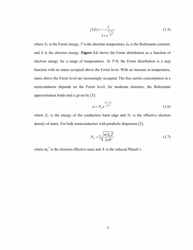
3
1( )1
F
B
E Ek T
f Ee
−=
+
(1.5)
where EF is the Fermi energy, T is the absolute temperature, kB is the Boltzmann constant,
and E is the electron energy. Figure 1.1 shows the Fermi distribution as a function of
electron energy for a range of temperatures. At T=0, the Fermi distribution is a step
function with no states occupied above the Fermi level. With an increase in temperature,
states above the Fermi level are increasingly occupied. The free carrier concentration in a
semiconductor depends on the Fermi level; for moderate densities, the Boltzmann
approximation holds and is given by [3]:
F C
B
E Ek T
Cn N e−
= (1.6)
where EC is the energy of the conduction band edge and NC is the effective electron
density of states. For bulk semiconductors with parabolic dispersion [3],
*
222
e BC
m k TNπ
=h
(1.7)
where me* is the electron effective mass and h is the reduced Planck’s.
4
1.1.3 How does temperature affect the scattering of free carriers?
Electrons traveling through a semiconductor lose energy through collisions with lattice
vibrations. The lattice vibration quantum, known as the phonon, has a frequency
distribution governed by Bose-Einstein statistics [4]:
1
1Bk T
ne
ω ω=
−h
(1.8)
where ω is the radial frequency. The dispersion relation for phonons is dependent on
material properties such as the speed of sound and interatomic potentials. The lowest
energy branch of phonons, known as acoustic phonons, has a dispersion which passes
through 0 and which can be written at low energies as [4]:
sv qω = (1.9)
where vs is the speed of sound and q is the phonon wavevector. Interactions between
electrons and phonons depend on the displacements of atoms from their equilibrium
positions. The perturbation potentials for electron-phonon interactions can be written as
[5]:
Figure 1.1. Effect of temperature on Fermi distribution
5
Acoustic phonons: ~APuU Dx
∂∂
(1.10)
Optical phonons: ~OP oU D u (1.11)
where u is the atomic displacement from equilibrium position, and D is a deformation
potential for acoustic phonons and D0 for optical phonons. With an increase in
temperature, the displacements of atoms about their equilibrium positions increase, and
as a result, the scattering of electrons with phonons is expected to increase. With an
increase in temperature, higher energy phonons are occupied which can also lead to an
increase in scattering rate.
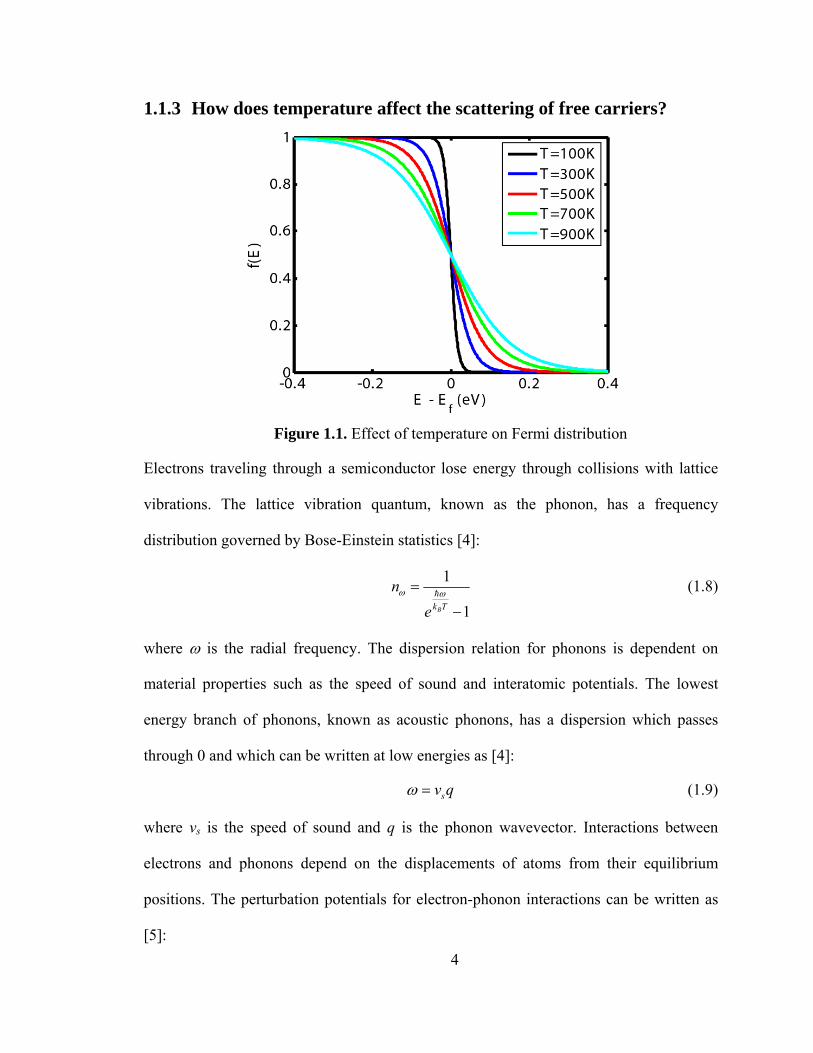
1.1.4 How does temperature affect scattering of phonons?
The scattering of phonons determines the thermal conductivity of materials. For
semiconductors, the dominating mechanisms for scattering of phonons are:
1) Phonon-Phonon scattering
2) Phonon impurity scattering
3) Phonon boundary scattering
The thermal conductivity can be written as [4]:
2
0
12
k v C dωτ ω∞
= ∫ (1.12)
Where v is the group velocity of phonons, τ is the scattering time, and, Cω is the specific
heat capacity per unit frequency at temperature T and is given by [4]:
6
( ) dnC DdT
ωω ω ω= h (1.13)
where D(ω) is the density of states of phonons. At high temperatures, the scattering is
dominated by phonon-phonon scattering, whose scattering rate can be written as [4]:
3 21 DbTBe Tθ
ωτ
−= (1.14)
where B and b are constants and θD is Debye temperature. This scattering gives the
temperature dependence of thermal conductivity as [4]:
1kT
∝ (1.15)
At low temperatures, where phonon occupation is low, the dominating scattering
mechanism is boundary scattering. The scattering rate for phonon boundary scattering
can be written as [4]:
1 sbLν
τ= (1.16)
Figure 1.2 Thermal conductivity of GaAs as a function of temperature. Low temperature thermal conductivity is determined by boundary scattering, while, high temperature thermal conductivity is determined by phonon scattering.
7
where bs is shape factor, L is size of grains. The thermal conductivity at low temperature
has a temperature dependence given by [4]:
3k T∝ (1.17)
1.2 Overview of work This work is focused on understanding and applying thermal effects to derive electronic
structure and transport properties in organic and inorganic semiconductors.
Chapter 2 gives an introduction to thermoelectric energy conversion and the
thermoelectric figure of merit (ZT). Thermoelectric generators are discussed, and their
performance is compared to other heat engines.
Chapter 3 is focused on nanostructured materials for high efficiency
thermoelectric energy conversion. As will be shown, the existing efficiencies of bulk
thermoelectric materials are insufficient to compete with gas and steam compression
cycle based systems. The fundamental cause is the inherent tradeoff between the
electrical conductivity and Seebeck coefficient with increasing doping in semiconductors.
We describe the motivation for nanostructured materials in which the electronic density
of states is increased at the band edge, and use InAs/GaAs and Ge/Si as model material
systems to demonstrate that 1D transport is achievable in composites which have
quantum dots aligned in 1 dimension. We show that this geometry of incorporating
aligned quantum dot in a matrix can result in a large increase in ZT.
Chapter 4 is focused on the design of integrated thermoelectric coolers for
optoelectronic devices. Although thermoelectric coolers suffer from a low COP, they are
suitable for microscale spot-cooling applications that require the cooler to be fabricated in
an integrated growth process using epitaxy. ZT values for small barrier mercury cadmium
8
telluride superlattices, used to make infrared detectors, are characterized using a steady-
state differential measurement. Coupled electrothermal simulations are performed, based
on measured electrical and thermal properties, to optimize the geometry of a
thermoelectric cooler monolithically integrated with an infrared detector pixel for
maximum cooling.
Chapter 5 is focused on designing thermoelectric power generators for energy
scavenging application. Similar to thermoelectric coolers, thermoelectric generators
suffer from low conversion efficiencies compared to steam or internal combustion
engines. However, many energy scavenging applications require scalable and low-cost
devices. In particular, we study textile-based geometries for thin-film thermoelectric
elements that are fabricated on flexible polymer fibers. The geometry of convectively-
cooled single-fiber thermoelectric generators is optimized based on a measured effective
heat transfer coefficient. Of many multi-fiber multi-thermocouple geometries possible,
we focus on simple weave textile geometries, fabricating plain weave thermoelectric
generators by a combination of thermal evaporation and electroless plating of metals.
Chapter 6 gives an introduction to organic photovoltaics, in which thermally
activated transport of excitons and charge carriers mediates energy conversion. In this
chapter, I briefly discuss the physics of light absorption, exciton formation and transport,
highlighting the importance of exciton disassociation through the formation of charge
transfer states. This chapter serves as background to Chapter 7, in a new characterization
technique is introduced for organic semiconductors
Chapter 7 examines the effect of temperature on the electronic structure of
organic semiconductors. Temperature modulation spectroscopy is proposed and applied
to organic semiconductors for the first time. Using a phase-sensitive detection technique,
9
we measure the modulation in optical transmission spectrum caused by a periodic change
in temperature for copper phthalocyanine. This modulation spectrum is used to determine
excitonic transitions and the temperature dependences of oscillator strength, transition
energy, and lifetime broadening. A clear difference in the temperature dependence of
oscillator strength is observed for Frenkel and charge transfer (CT) excitons, motivating
the broad use of this technique to determine exciton character and measure electronic
coupling parameters for organic semiconductors.
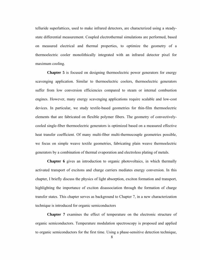
Figure 1.3 shows an overview of work in this thesis.
Figure 1.3. An overview of the work in this thesis.
10
Chapter 2
Thermoelectric energy conversion
2.1 Thermoelectric transport
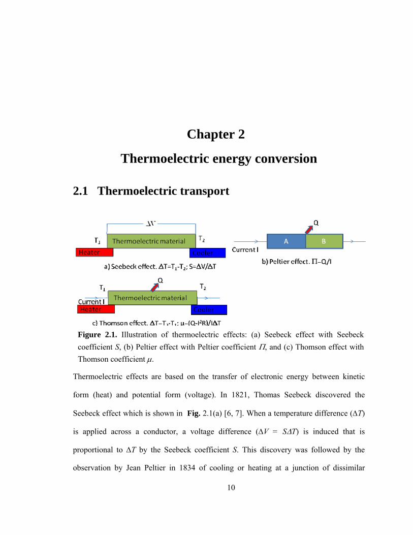
Thermoelectric effects are based on the transfer of electronic energy between kinetic
form (heat) and potential form (voltage). In 1821, Thomas Seebeck discovered the
Seebeck effect which is shown in Fig. 2.1(a) [6, 7]. When a temperature difference (ΔT)
is applied across a conductor, a voltage difference (ΔV = SΔT) is induced that is
proportional to ΔT by the Seebeck coefficient S. This discovery was followed by the
observation by Jean Peltier in 1834 of cooling or heating at a junction of dissimilar
Figure 2.1. Illustration of thermoelectric effects: (a) Seebeck effect with Seebeck coefficient S, (b) Peltier effect with Peltier coefficient Π, and (c) Thomson effect with Thomson coefficient μ.
11
metals on passing an electric current. This is known as the Peltier effect and is shown in
Fig. 2.1(b) [6]. The Peltier coefficient is defined as the heat absorbed or rejected (Q) at
the junction per unit electric current (Π=Q/I), and is related to the Seebeck coefficient by
Π=T×S. A third thermoelectric effect in which a current carrying conductor is heated or
cooled in the presence of a temperature gradient was discovered by William Thomson
(Lord Kelvin) in 1855. This is known as Thomson effect [6] and is shown in Fig. 2.1(c);
the corresponding constant is known as the Thomson coefficient γ. Together, these three
effects compose thermoelectric phenomena.
2.2 Thermoelectric devices
2.2.1 Thermoelectric power generator
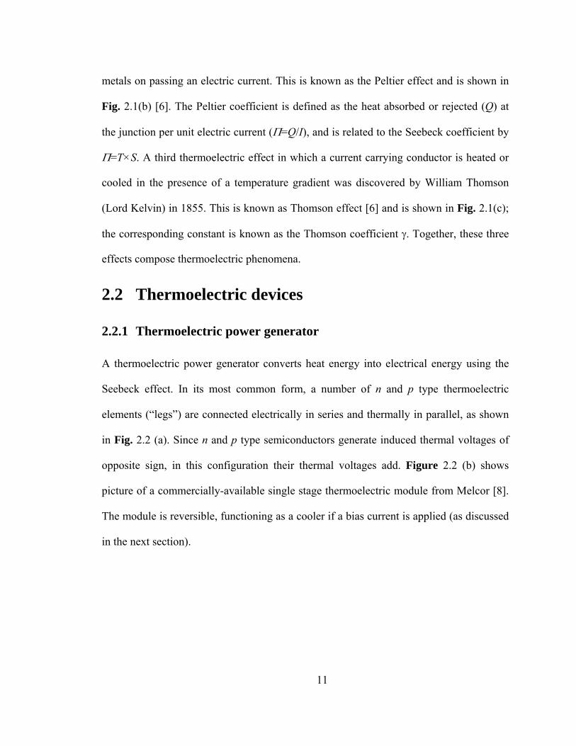
A thermoelectric power generator converts heat energy into electrical energy using the
Seebeck effect. In its most common form, a number of n and p type thermoelectric
elements (“legs”) are connected electrically in series and thermally in parallel, as shown
in Fig. 2.2 (a). Since n and p type semiconductors generate induced thermal voltages of
opposite sign, in this configuration their thermal voltages add. Figure 2.2 (b) shows
picture of a commercially-available single stage thermoelectric module from Melcor [8].
The module is reversible, functioning as a cooler if a bias current is applied (as discussed
in the next section).
12
In order to approximate the efficiency of thermoelectric energy conversion for the
module, we assume that both the heat sink and heat source function as thermal reservoirs
and have temperatures that are independent of heat flux. Under these conditions, the rate
of heat transfer from the hot side can be written as [9]:
212h hQ K T T I I Rα= Δ + − (2.1)
where Qh is the rate of heat transfer at hot side, k is the net thermal conductivity, α is the
net Seebeck coefficient, Th is the hot side temperature, I is the current through the device,
and R is the total electrical resistance of the device. Here we have assumed that the
Seebeck coefficient of metal used to form the junctions is negligible, and that half of the
resistive (I2R) heating goes to each junction. The net thermal conductivity for thermal
elements in parallel can be written as [9]:
pnn p
n p
AAk k kl l
= + (2.2)
where kn, An, and ln are the thermal conductivity, cross-sectional area, and length of the
n type legs, and kp, Ap, and lp are the thermal conductivity, cross-sectional area, and
Figure 2.2. (a) Schematic of a thermoelectric power generator (b) picture of commercially available thermoelectric unit from Melcor.
13
length of the p type legs. The net Seebeck coefficient is given by [9]:
n pα α α= + (2.3)
where αn and αp are the Seebeck coefficients of the n and p type materials. The efficiency
of the thermoelectric generator is given by
2
0
h
I RQ
η = (2.4)
which reaches a maximum value (for an optimal leg geometry) of [9]:
max
1 11
1
avgh
ccavg
h
ZTTTT ZTT
η+ −⎛ ⎞
= −⎜ ⎟⎝ ⎠ + +
(2.5)
where Z is the dimensionless thermoelectric figure of merit defined by:
2
Zkα
ρ= (2.6)
and Tavg is the average temperature of heat sink and source given by
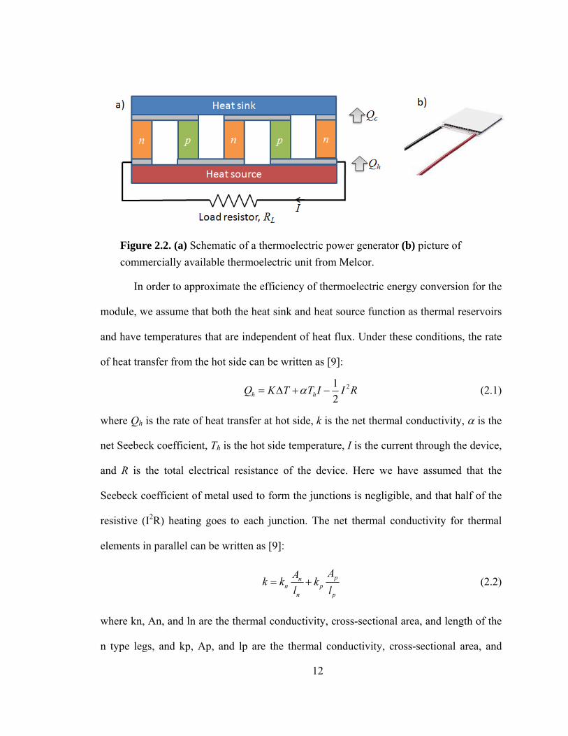
Figure 2.3. Maximum efficiency of thermoelectric power generator as a function of heat source temperature for different values of the figure of merit.
14
2
c hav
T TT += (2.7)
Figure 1.3 shows the maximum efficiency vs. hot side temperature for different values of
ZTavg, assuming a cold side temperature of 27°C. It is evident that the maximum
efficiency depends on the dimensionless figure of merit. Steam engines used in fossil fuel
fired power plants work at Th ~ 700 K at efficiencies up to 40%. Internal combustion
engines work at higher temperatures of Th ~ 1000 K but also have larger losses leading to
lower efficiencies in the range of 20-35%. Hence, a ZTavg of greater than 3 is required to
achieve efficiencies close to IC engines.
2.2.2 Thermoelectric cooler
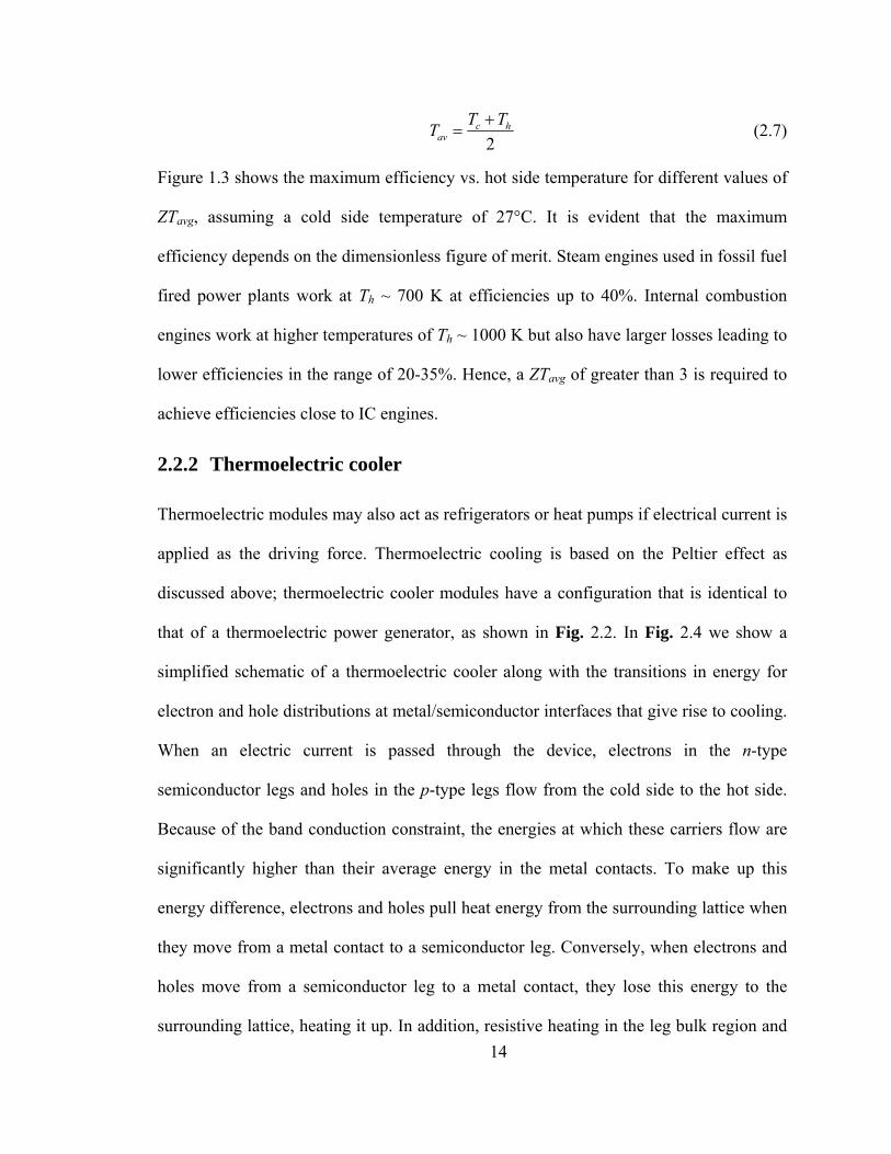
Thermoelectric modules may also act as refrigerators or heat pumps if electrical current is
applied as the driving force. Thermoelectric cooling is based on the Peltier effect as
discussed above; thermoelectric cooler modules have a configuration that is identical to
that of a thermoelectric power generator, as shown in Fig. 2.2. In Fig. 2.4 we show a
simplified schematic of a thermoelectric cooler along with the transitions in energy for
electron and hole distributions at metal/semiconductor interfaces that give rise to cooling.
When an electric current is passed through the device, electrons in the n-type
semiconductor legs and holes in the p-type legs flow from the cold side to the hot side.
Because of the band conduction constraint, the energies at which these carriers flow are
significantly higher than their average energy in the metal contacts. To make up this
energy difference, electrons and holes pull heat energy from the surrounding lattice when
they move from a metal contact to a semiconductor leg. Conversely, when electrons and
holes move from a semiconductor leg to a metal contact, they lose this energy to the
surrounding lattice, heating it up. In addition, resistive heating in the leg bulk region and
15
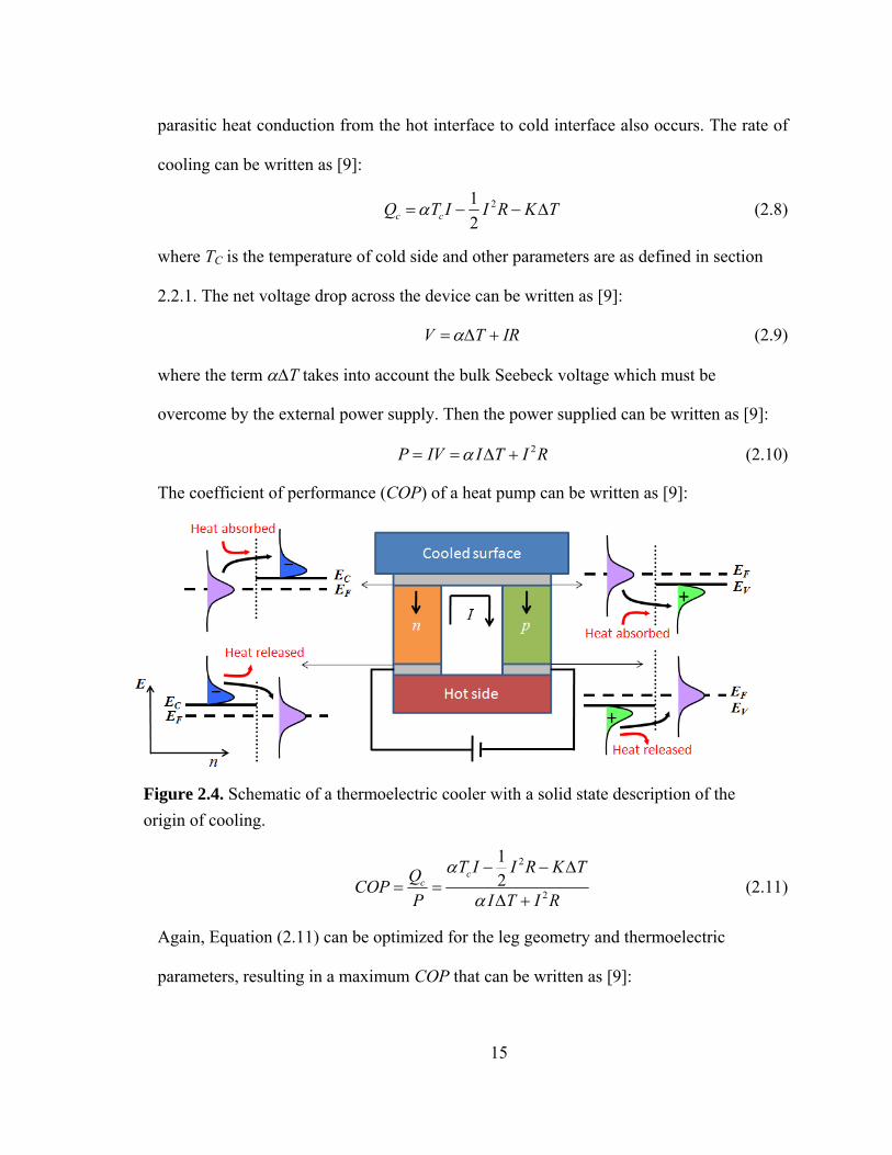
parasitic heat conduction from the hot interface to cold interface also occurs. The rate of
cooling can be written as [9]:
212c cQ T I I R K Tα= − − Δ (2.8)
where TC is the temperature of cold side and other parameters are as defined in section
2.2.1. The net voltage drop across the device can be written as [9]:
V T IRα= Δ + (2.9)
where the term αΔT takes into account the bulk Seebeck voltage which must be
overcome by the external power supply. Then the power supplied can be written as [9]:
2P IV I T I Rα= = Δ + (2.10)
The coefficient of performance (COP) of a heat pump can be written as [9]:
2
2
12c
cT I I R K TQCOP
P I T I R
α
α
− − Δ= =
Δ + (2.11)
Again, Equation (2.11) can be optimized for the leg geometry and thermoelectric
parameters, resulting in a maximum COP that can be written as [9]:
Figure 2.4. Schematic of a thermoelectric cooler with a solid state description of the origin of cooling.
16
max
1
1 1
havg
c c
h c avg
TZTT T
T T ZTη
+ −⎛ ⎞
= ⎜ ⎟− + +⎝ ⎠ (2.12)
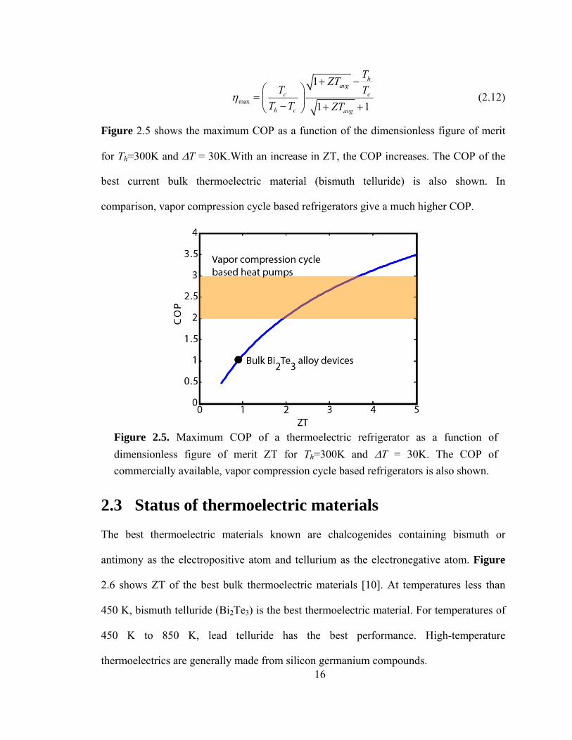
Figure 2.5 shows the maximum COP as a function of the dimensionless figure of merit
for Th=300K and ΔT = 30K.With an increase in ZT, the COP increases. The COP of the
best current bulk thermoelectric material (bismuth telluride) is also shown. In
comparison, vapor compression cycle based refrigerators give a much higher COP.
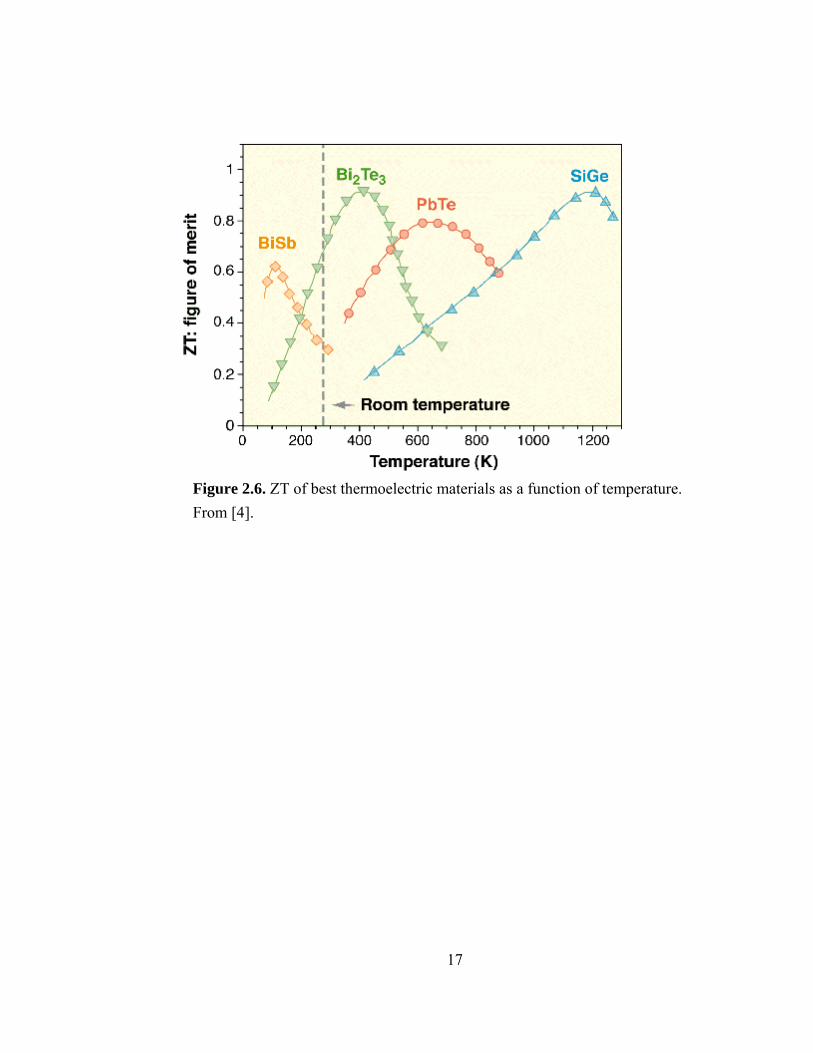
2.3 Status of thermoelectric materials The best thermoelectric materials known are chalcogenides containing bismuth or
antimony as the electropositive atom and tellurium as the electronegative atom. Figure
2.6 shows ZT of the best bulk thermoelectric materials [10]. At temperatures less than
450 K, bismuth telluride (Bi2Te3) is the best thermoelectric material. For temperatures of
450 K to 850 K, lead telluride has the best performance. High-temperature
thermoelectrics are generally made from silicon germanium compounds.
Figure 2.5. Maximum COP of a thermoelectric refrigerator as a function of dimensionless figure of merit ZT for Th=300K and ΔT = 30K. The COP of commercially available, vapor compression cycle based refrigerators is also shown.
17
Figure 2.6. ZT of best thermoelectric materials as a function of temperature. From [4].
18
Chapter 3
Thermoelectric properties of aligned quantum dot
chains
3.1 Theory of thermoelectric transport In this section we look at the tradeoff between electrical conductivity and Seebeck
coefficient that limits the thermoelectric power factor, and consequently, the
thermoelectric figure of merit of bulk materials. Our discussion follows a similar path to
that given in [4, 11]. The transport of charge carriers is governed by the Boltzmann
transport equation, which can be written as:
vv rcollision
f F ff ft m t
∂ ∂+ ⋅∇ + ⋅∇ =
∂ ∂
rr (3.1)
where f is the distribution function of charge carriers and is a function of time, spatial
coordinates, and momentum coordinates, vr is the velocity of the charge carriers, and Fr
is the force acting on charge carriers. We make simplifying assumptions of steady-state
electron transport in 1D along the x direction, a small change in the distribution function
and its gradient on application of an electric field, and elastic scattering. Given a force -
eEx on electrons, where Ex is the applied electric field along the x direction, Equation
(3.1) can be written as:
19
0 0 0xx
x
f eE f f fvx m v τ
∂ ∂ −− = −
∂ ∂ (3.2)
where f0 is the equilibrium distribution function and τ is the momentum relaxation time.
The carrier distribution can then be written as:
0 00
xx
x
f eE ff f vx m v
τ⎛ ⎞∂ ∂
= − −⎜ ⎟∂ ∂⎝ ⎠ (3.3)
The equilibrium distribution for electrons is given by the Fermi-Dirac distribution:
01
1f
B
E Ek T
f
e−=
+
(3.4)
where E is the energy of electrons, Ef is the Fermi level, kB is the Boltzmann constant,
and T is the absolute temperature. The first term in parentheses on the right side of
Equation (3.3) is a gradient in the distribution function due to a change in either the
Fermi level or the carrier temperature with position. The second term is due to the force
of the applied field on the electron distribution. The spatial gradient of the distribution
function can be written as:
0 0 0f
f
Ef f f Tx E x T x
∂∂ ∂ ∂ ∂= +
∂ ∂ ∂ ∂ ∂ (3.5)
Using Equation (3.4) this can be further simplified as:
0 0 0f f
B
E E Ef f f Tx E x k T E x
∂ −∂ ∂ ∂ ∂= − −
∂ ∂ ∂ ∂ ∂ (3.6)
The current density can be written as:
( )3
22
x x y zj ev fdk dk dkπ
∞ ∞ ∞
−∞ −∞ −∞
= − ∫ ∫ ∫ (3.7)
Substituting equation (3.3) and (3.6) in this expression yields:
20
( )
0 0 003
22
f f xx x x x y z
B x
E E Ef f eE fT Ej ev f v v dk dk dkE x k T E x m E v
τπ
∞ ∞ ∞
−∞ −∞ −∞
⎛ ⎞∂ −⎛ ⎞∂ ∂ ∂∂ ∂= − − − − −⎜ ⎟⎜ ⎟⎜ ⎟∂ ∂ ∂ ∂ ∂ ∂⎝ ⎠⎝ ⎠
∫ ∫ ∫
(3.8)
The integral over f0 is zero since the current densities in the +x and –x directions are the
same for the equilibrium distribution. Equation 1.8 can then be reduced to:
11 121 f
x
E Tj L E Le x x
∂⎛ ⎞ ∂⎛ ⎞= + + −⎜ ⎟ ⎜ ⎟∂ ∂⎝ ⎠⎝ ⎠ (3.9)
where L11 and L12 are defined as:
( )
2 011 3
22
x x y zfL ev dk dk dkE
τπ
∞ ∞ ∞
−∞ −∞ −∞
∂⎛ ⎞= −⎜ ⎟∂⎝ ⎠∫ ∫ ∫ (3.10)
( )
2 012 3
22
fx x y z
B
E E fL ev dk dk dkk T E
τπ
∞ ∞ ∞
−∞ −∞ −∞
− ∂⎛ ⎞= − −⎜ ⎟∂⎝ ⎠∫ ∫ ∫ (3.11)
The electrochemical potential can be written as:
fc EEe e
φ = − − (3.12)
where Ec is the conduction band edge and Ef is measured with respect to Ec. The gradient
of electrochemical potential is given by:
1 fx
EF
x e xφ ∂∂
= −∂ ∂
(3.13)
where ( )1/ /x cF e E x= − ∂ ∂ is the external applied electric field. Equation (3.9) can then
be written as:
11 12Tj L L
x xφ∂ ∂⎛ ⎞ ⎛ ⎞= − + −⎜ ⎟ ⎜ ⎟∂ ∂⎝ ⎠ ⎝ ⎠
(3.14)
In the case of no temperature gradient, the proportionality between electron current
density and the gradient of electrochemical potential is given by the electrical
21
conductivity. Hence, electrical conductivity σ can be written as:
11Lσ = (3.15)
In the case of a temperature gradient and open circuit, the proportionality between
induced voltage and the temperature gradient is given by Seebeck coefficient (S), which
can be written as:
12
11
//
LxST x Lφ−∂ ∂
= =∂ ∂
(3.16)
From Equation (3.11) we can see that the Seebeck coefficient is proportional to σ(E)(E-
Ef) where σ(E) is the integrand of L11. The Seebeck coefficient is proportional to the
average energy of electrons with respect to the Fermi energy under open circuit
condition, weighted by the electrical conductivity at each energy level occupied by an
electron. Hence, the Seebeck coefficient will be larger in magnitude if electrons carry
energy that is greater than or less than the Fermi energy. In contrast, the electrical
conductivity is maximized if the Fermi level lies in the conduction band, which results in
a large number of electrons participating in transport. Figure 3.1(a) shows the density of
Figure 3.1. (a) 3D electron density of states, (b) Fermi distribution, (c) derivative of Fermi function, (d) electrical conductivity, and (e) Seebeck coefficient as a function of energy.
22
states of electrons in bulk semiconductors. Figs 3.1(b) and (c) show the Fermi function
and its derivative with respect to energy. The derivative is important because only energy
levels with nonzero values of the derivative participate in transport. Fig. 3.1 (d) shows
the electrical conductivity, which is a convolution of the density of states and the
derivative of the Fermi function. It follows the derivative of Fermi function closely,
which implies that only electrons near the Fermi level can participate in charge transport.
For the Seebeck coefficient (shown in Fig. 3.1 (e)), the average energy with respect to the
Fermi energy must be taken into account. Electrons above and below the Fermi level
carry thermal energy in opposite directions (even though they travel in the same
direction) and hence their contributions to the Seebeck coefficient are of opposite sign.
3.2 Nanostructured materials for high efficiency
thermoelectric devices Nanostructured materials, which may be tailored for optimum transport of heat
and electricity, have been proposed for the next generation of thermoelectric materials
[12-15]. As seen in Section 2.1, the electrical conductivity and Seebeck coefficient have
opposite behavior as Fermi level is increased in bulk materials. Fermi level in
semiconductors increases with an increase in doping. The Seebeck coefficient can be
nonzero only if the energy distribution of conducting carriers is asymmetric about the
Fermi level. This implies that the Fermi level cannot be too deep in the conduction band.
However, if it moves too close to the band edge, the density of states becomes small,
leading to a reduction in electrical conductivity. If the density of states at the band edge
can be increased, however, then a higher electrical conductivity can be achieved without
sacrificing Seebeck coefficient, leading to a higher ZT. Low dimensional materials such
23
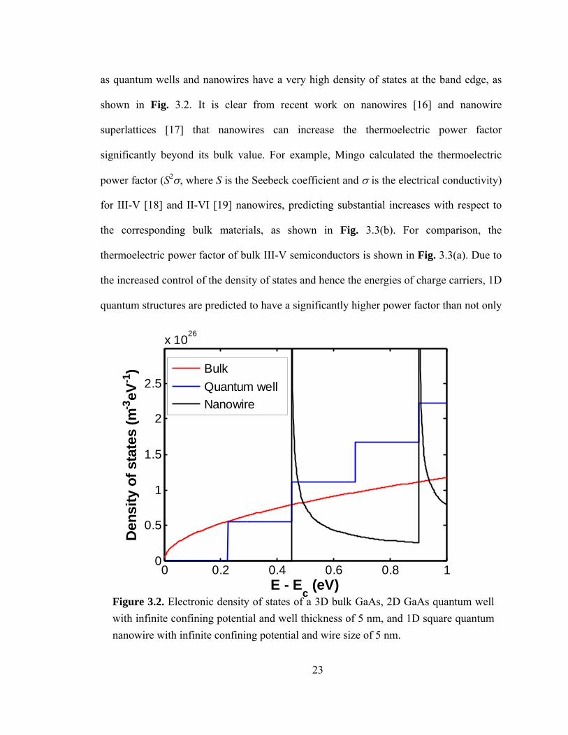
as quantum wells and nanowires have a very high density of states at the band edge, as
shown in Fig. 3.2. It is clear from recent work on nanowires [16] and nanowire
superlattices [17] that nanowires can increase the thermoelectric power factor
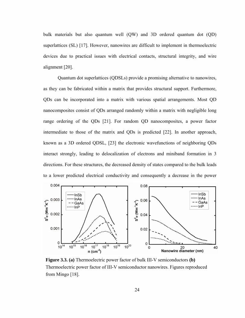
significantly beyond its bulk value. For example, Mingo calculated the thermoelectric
power factor (S2σ, where S is the Seebeck coefficient and σ is the electrical conductivity)
for III-V [18] and II-VI [19] nanowires, predicting substantial increases with respect to
the corresponding bulk materials, as shown in Fig. 3.3(b). For comparison, the
thermoelectric power factor of bulk III-V semiconductors is shown in Fig. 3.3(a). Due to
the increased control of the density of states and hence the energies of charge carriers, 1D
quantum structures are predicted to have a significantly higher power factor than not only
Figure 3.2. Electronic density of states of a 3D bulk GaAs, 2D GaAs quantum well with infinite confining potential and well thickness of 5 nm, and 1D square quantum nanowire with infinite confining potential and wire size of 5 nm.
0 0.2 0.4 0.6 0.8 10
0.5
1
1.5
2
2.5
x 1026
E - Ec (eV)
Den
sity
of s
tate
s (m
-3eV
-1) Bulk
Quantum wellNanowire
24
bulk materials but also quantum well (QW) and 3D ordered quantum dot (QD)
superlattices (SL) [17]. However, nanowires are difficult to implement in thermoelectric
devices due to practical issues with electrical contacts, structural integrity, and wire
alignment [20].
Quantum dot superlattices (QDSLs) provide a promising alternative to nanowires,
as they can be fabricated within a matrix that provides structural support. Furthermore,
QDs can be incorporated into a matrix with various spatial arrangements. Most QD
nanocomposites consist of QDs arranged randomly within a matrix with negligible long
range ordering of the QDs [21]. For random QD nanocomposites, a power factor
intermediate to those of the matrix and QDs is predicted [22]. In another approach,
known as a 3D ordered QDSL, [23] the electronic wavefunctions of neighboring QDs
interact strongly, leading to delocalization of electrons and miniband formation in 3
directions. For these structures, the decreased density of states compared to the bulk leads
to a lower predicted electrical conductivity and consequently a decrease in the power
Figure 3.3. (a) Thermoelectric power factor of bulk III-V semiconductors (b) Thermoelectric power factor of III-V semiconductor nanowires. Figures reproduced from Mingo [18].
25
factor. Here we calculate the thermoelectric properties of a QD chain nanocomposite,
which consists of a QDSL with a 2D pattern of QDs that are aligned to form chains [24-
28], with negligible interactions between neighboring chains. This geometry leads to
confinement of electrons in the chains, with carrier transport through minibands
occurring only along the chains. We predict that QD chain nanocomposites can have
greatly enhanced thermoelectric properties due to 1D carrier transport along the chains,
analogous to transport in nanowires or nanowire SLs. In both nanowires and QD chain
nanocomposites, a reduction in thermal conductivity (λ) with respect to the bulk is
expected to lead to further enhancement in the thermoelectric figure of merit ZT =
S2σ/λ [29−31]. For example, while the bulk thermal conductivities of GaAs and Si are 55
W/mK and 130 W/mK respectively, the addition of ErAs nanoparticles to InGaAs has
been shown to decrease its thermal conductivity by a factor of 2 [30]. Here we focus on
the electronic contribution to ZT (S2σ) for two material systems (InAs/GaAs and Ge/Si)
that are frequently utilized in electronic and optoelectronic applications. Both are
compressively strained semiconductor systems in which Stranski-Krastanow (SK) growth
leads to self-assembled QD formation; control of the ordering of such QDs is an active
area of investigation [32, 33]. For GaAs (Si) with embedded InAs (Ge) QD chains, we
calculate an increase in the thermoelectric power factor by a factor of 3 (1.5) in
comparison with the corresponding GaAs (Si) bulk.
26
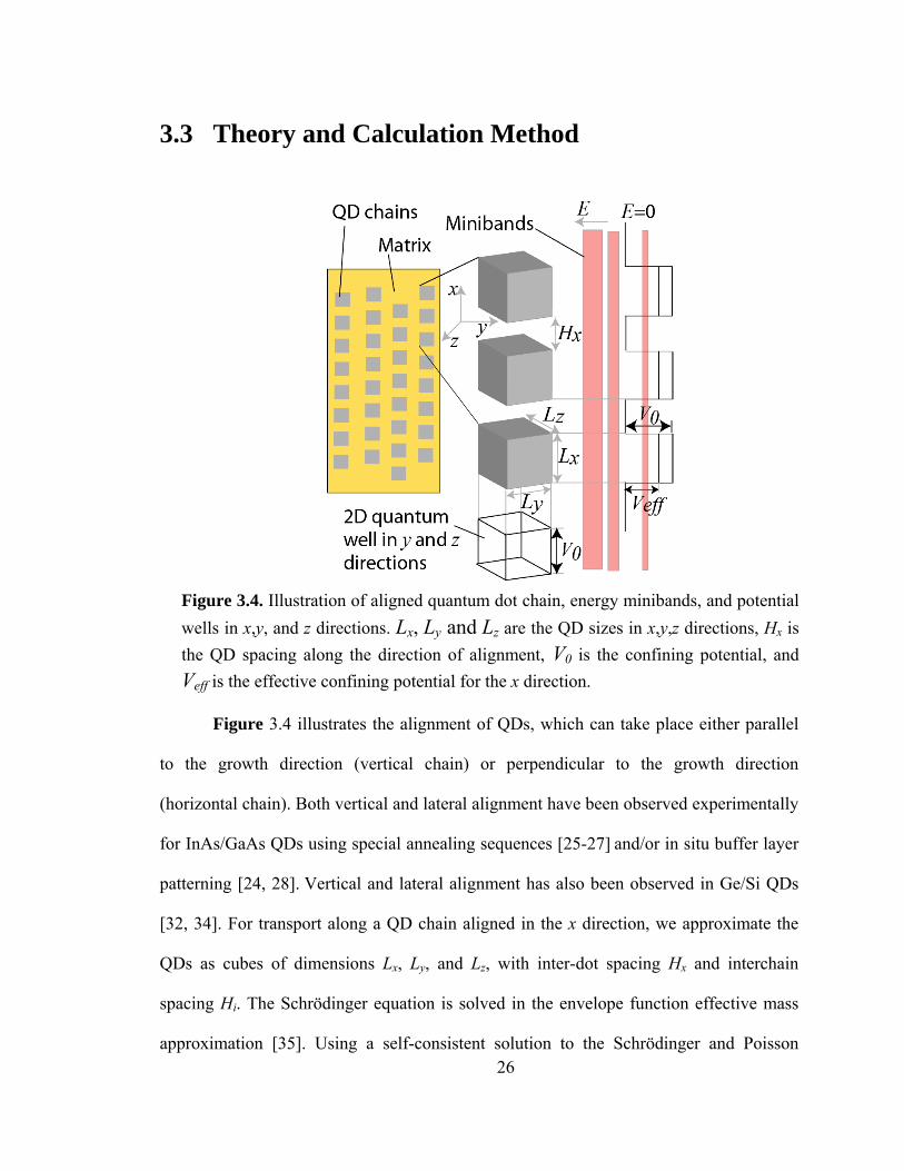
3.3 Theory and Calculation Method
Figure 3.4 illustrates the alignment of QDs, which can take place either parallel
to the growth direction (vertical chain) or perpendicular to the growth direction
(horizontal chain). Both vertical and lateral alignment have been observed experimentally
for InAs/GaAs QDs using special annealing sequences [25-27] and/or in situ buffer layer
patterning [24, 28]. Vertical and lateral alignment has also been observed in Ge/Si QDs
[32, 34]. For transport along a QD chain aligned in the x direction, we approximate the
QDs as cubes of dimensions Lx, Ly, and Lz, with inter-dot spacing Hx and interchain
spacing Hi. The Schrödinger equation is solved in the envelope function effective mass
approximation [35]. Using a self-consistent solution to the Schrödinger and Poisson
Figure 3.4. Illustration of aligned quantum dot chain, energy minibands, and potential wells in x,y, and z directions. Lx, Ly and Lz are the QD sizes in x,y,z directions, Hx is the QD spacing along the direction of alignment, V0 is the confining potential, and Veff is the effective confining potential for the x direction.
27
equations, the error in the position of the energy bands due to neglecting the effect of
band-bending has been shown to be less than 5% [36]. Hence, for ease of calculation,
band-bending is neglected. In the directions perpendicular to the QD chain, 2D
confinement is approximated by two 1D QWs with confined subband energy levels [36].
Using these subband energy levels, an effective potential along the QD chain (Veff) is
calculated, as illustrated in Fig. 3.4. Veff is then used in a Kronig-Penny model to
calculate the miniband energy levels as a function of kx, i.e. the miniband dispersion
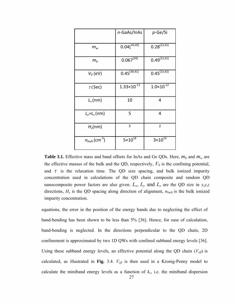
Table 3.1. Effective mass and band offsets for InAs and Ge QDs. Here, mb and mw are the effective masses of the bulk and the QD, respectively, V0 is the confining potential, and τ is the relaxation time. The QD size spacing, and bulk ionized impurity concentration used in calculations of the QD chain composite and random QD nanocomposite power factors are also given. Lx, Ly and Lz are the QD size in x,y,z directions, Hx is the QD spacing along direction of alignment, nbulk is the bulk ionized impurity concentration.
n‐GaAs/InAs p‐Ge/Si
mw 0.04[39,40] 0.28[23,42]
mb 0.067[39] 0.49[23,42]
V0 (eV) 0.45[39,41] 0.45[23,42]
τ (Sec) 1.33×10‐13 1.0×10‐12
Lx (nm) 10 4
Ly=Lz (nm) 5 4
Hx(nm) 5 2
nbulk (cm‐3) 5×10¹⁸ 3×10¹⁹
28
E(kx). Finally, E(kx) is used to calculate the density of states 2/(Ly×Lz)×dkx/dE. The
electronic transport properties σ and S are then calculated using the Boltzmann transport
equation by summing over all n minibands [11]:
( )22
0,v
x x
x x
L H
x n x xny z
L H
fq k dkL L E
π
π
τσπ
+
−+
∂⎛ ⎞= −⎜ ⎟∂⎝ ⎠∑ ∫ (3.17)
( ) ( )( )
( )
2
2
0,
0,
v
1
v
x x
x x
x x
x x
L H
x n x n x f xn
L H
L H
x n x xn
L H
fk E k E dkE
SqT
fk dkE
π
π
π
π
+
−+
+
−+
∂⎛ ⎞− −⎜ ⎟∂⎝ ⎠−
=
∂⎛ ⎞−⎜ ⎟∂⎝ ⎠
∑ ∫
∑ ∫
(3.18)
Here, the integration is over the miniband quasi Brillouin zone [37], q is the electron
charge, τ is the relaxation time for carriers, T is the temperature, f0 is the equilibrium
Fermi distribution, Ef is the Fermi level, kx is the wavevector for minibands along the QD
chain, E(kx) is the dispersion relation obtained from the solution of the Schrödinger wave
equation, and vx is the electron group velocity given by:
( ) ( ),
1v n xx n x
x
E kk
k∂
=∂h
(3.19)
We have studied two different material systems: InAs/GaAs and Ge/Si, which have
different confining potentials and free carrier effective masses. For InAs/GaAs (Ge/Si),
the band offset is dominated by the conduction (valence) band offset [38]; hence, we
study n-InAs/GaAs and p-Ge/Si. A Fermi level of zero corresponds to the GaAs
conduction band edge (silicon valence band edge) for the InAs/GaAs (Ge/Si) system. We
use literature values of conduction and valence band offsets and QD carrier effective
29
masses that are corrected for strain and confinement effects, as given in Table 3.1, which
are taken from Refs. [39-41] for InAs/GaAs and [23, 42] for Ge/Si. For all calculations,
we assume room temperature (300 K) and a constant relaxation time, with values listed in
Table 3.1. For the InAs/GaAs system, τ is derived from the mobility in bulk GaAs at the
doping level that corresponds to a Fermi level position at the conduction band edge. For
the Ge/Si system, τ is taken from Ref. [23].
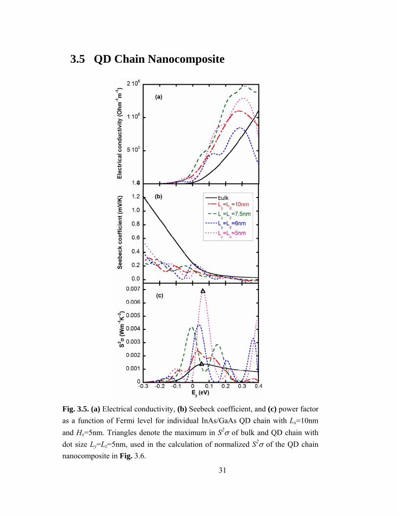
3.4 Single Quantum Dot Chains: Size Effects In this section, we examine the effects of QD size on the thermoelectric properties
of a single QD chain. Similar trends were observed for both Ge/Si and InAs/GaAs
systems; for simplicity, we focus on the InAs/GaAs system. Figures 3.5 (a) and 3.5 (b)
show σ and S as a function of the Fermi level for a single InAs/GaAs QD chain, in
comparison with that of bulk GaAs. Oscillations in σ and S occur as the Fermi level is
increased and swept through the minibands. Similar oscillations as a function of Fermi
level have been predicted for various nanostructured materials including 3D ordered
QDSLs [23, 37], quantum well (QW) SLs [43], and nanowire SLs [17]. For 1D transport
(along an individual nanowire), σ is inversely proportional to the wire diameter [16].
Additionally, for QD chains, an increase in σ is predicted to occur with increasing QD
diameter due to an increase in the number of subbands per QD, leading to a greater
number of QD chain minibands. Since the total density of states at any energy level is the
summation of the density of states for each individual miniband at that energy level, the
presence of multiple minibands increases the total density of states and hence σ.
In Fig. 3.5 (c), the power factor (S2σ) is plotted as a function of Fermi level for a
variety of QD sizes, in comparison with that of bulk GaAs. In all cases, S2σ is maximized

30
when the Fermi level lies within a few kBT of the GaAs matrix conduction band edge. For
higher Fermi levels, the minibands form a nearly continuous band, leading to low values
of S and S2σ.
31
3.5 QD Chain Nanocomposite
Fig. 3.5. (a) Electrical conductivity, (b) Seebeck coefficient, and (c) power factor as a function of Fermi level for individual InAs/GaAs QD chain with Lx=10nm and Hx=5nm. Triangles denote the maximum in S2σ of bulk and QD chain with dot size Ly=Lz=5nm, used in the calculation of normalized S2σ of the QD chain nanocomposite in Fig. 3.6.
32
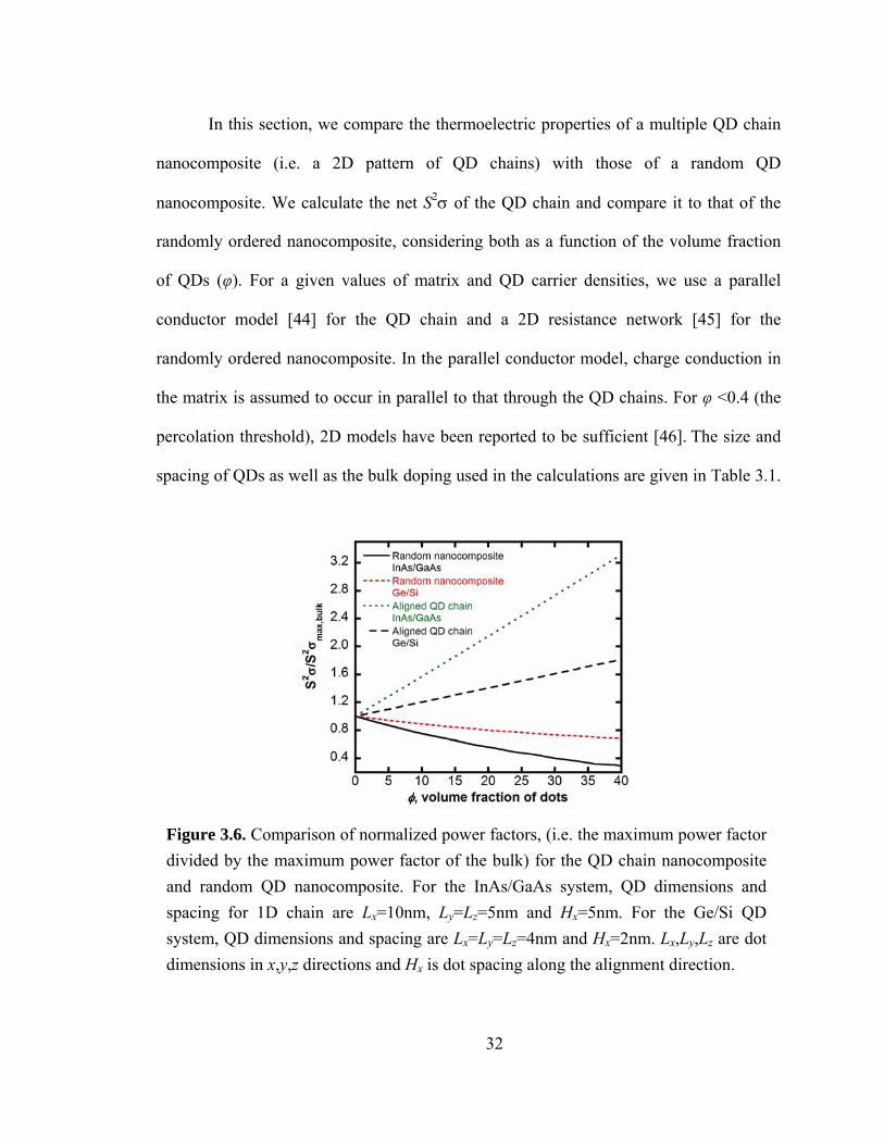
In this section, we compare the thermoelectric properties of a multiple QD chain
nanocomposite (i.e. a 2D pattern of QD chains) with those of a random QD
nanocomposite. We calculate the net S2σ of the QD chain and compare it to that of the
randomly ordered nanocomposite, considering both as a function of the volume fraction
of QDs (φ). For a given values of matrix and QD carrier densities, we use a parallel
conductor model [44] for the QD chain and a 2D resistance network [45] for the
randomly ordered nanocomposite. In the parallel conductor model, charge conduction in
the matrix is assumed to occur in parallel to that through the QD chains. For φ <0.4 (the
percolation threshold), 2D models have been reported to be sufficient [46]. The size and
spacing of QDs as well as the bulk doping used in the calculations are given in Table 3.1.
Figure 3.6. Comparison of normalized power factors, (i.e. the maximum power factor divided by the maximum power factor of the bulk) for the QD chain nanocomposite and random QD nanocomposite. For the InAs/GaAs system, QD dimensions and spacing for 1D chain are Lx=10nm, Ly=Lz=5nm and Hx=5nm. For the Ge/Si QD system, QD dimensions and spacing are Lx=Ly=Lz=4nm and Hx=2nm. Lx,Ly,Lz are dot dimensions in x,y,z directions and Hx is dot spacing along the alignment direction.
33
The bulk doping is chosen to correspond to the value which gives a maximum power
factor. The ionized impurity concentration in the QDs is then calculated using the Poisson
equation. The maximum S2σ of the InAs/GaAs QD chain occurs at Ef=0.064 eV above
the conduction band edge of bulk GaAs, which corresponds to a bulk doping
concentration of approximately 5×1018 cm-3 [11]. For Ge/Si QDs, the maximum S2σ
occurs at Ef=0.002 eV above the valence band edge of bulk Si, which corresponds to a
bulk doping concentration of approximately 1×1019 cm-3.
To compare the InAs/GaAs and Ge/Si systems, we plot the maximum S2σ of the
nanocomposite divided by the maximum S2σ of the bulk (GaAs or Si), i.e. the
"normalized" power factor, as a function of φ. This is shown in Fig. 3.6 for both multiple
QD chain and random nanocomposites. Since the parallel conductor model does not
include interactions between the bulk and QD chains or between neighboring QD chains,
the nanocomposite electrical conductivity (σnanocomposite) and Seebeck coefficient
(Snanocomposite) can be written as:
34
( )1nanocomposite chain chain bulk chainσ σ ϕ σ ϕ= + − (3.20)
( )( )
11
chain chain chain bulk bulk chainnanocomposite
chain chain bulk chain
S SS
σ ϕ σ ϕσ ϕ σ ϕ
+ −=
+ − (3.21)
Here, σchain and Schain (σbulk and Sbulk) are the electrical conductivity and Seebeck
coefficient of the QD chain (bulk) corresponding to the maximum in power factor of the
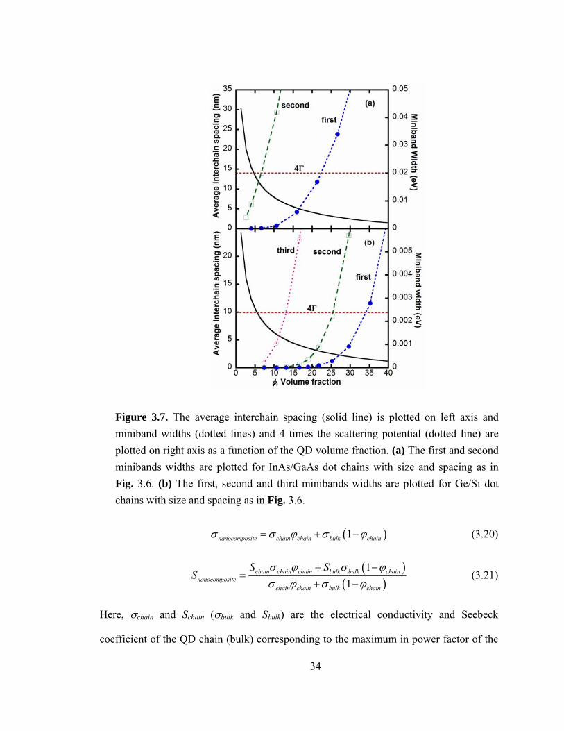
Figure 3.7. The average interchain spacing (solid line) is plotted on left axis and miniband widths (dotted lines) and 4 times the scattering potential (dotted line) are plotted on right axis as a function of the QD volume fraction. (a) The first and second minibands widths are plotted for InAs/GaAs dot chains with size and spacing as in Fig. 3.6. (b) The first, second and third minibands widths are plotted for Ge/Si dot chains with size and spacing as in Fig. 3.6.
35
QD chain (bulk), shown by the triangles in Fig. 3.5 (c). φchain= φ×(Lx+Hx)/Lx is the
volume fraction of QD chains. From Equation (3.20), it is evident that the σnanocomposite is
linearly dependent on φ. Due to the similarities in S for the bulk and QD chain,
Snanocomposite has a weak dependence on φ. Hence, for the multiple QD chain
nanocomposite, the normalized S2σ is linearly dependent on φ. For the random QD
nanocomposite, S2σ varies linearly with φ for low φ. For high φ, percolation effects lead
to saturation in S2σ. For aligned QDs with φ = 0.4, the normalized S2σ increases by more
than 300% (180%) compared to bulk InAs/GaAs (Ge/Si). This stands in stark contrast to
the random QD nanocomposite, for which the normalized S2σ decreases with increasing
φ due to the intrinsically lower S2σ of the QDs.
To achieve 1D transport along the chain, interactions between neighboring chains
must be negligible. Fig. 3.7 plots the values of φ and interchain spacing (Hi) for which
this assumption holds. As φ is increased, the spacing between QD chains is reduced. The
different regimes of charge transport in confined systems can be described using the
parameters of lateral interwell coupling (Δ/4) and scattering potential (Γ=ℏ/τ, where Δ is
the miniband width and τ is the relaxation time) [47]. When Δ/4<<Γ, there is negligible
miniband transport along the lateral direction (i.e. between the chains) [47]. In Fig.
3.7(a), for the InAs/GaAs system, Hi (left axis) and the first and second miniband widths
in the lateral direction (right axis) are plotted as a function of φ. For comparison, 4Γ is
also shown. For φ=0.06, corresponding to Hi=11 nm, miniband transport in the lateral
direction commences, and the assumption of negligible transport between the chains is no
longer valid. As shown in Fig. 3.6, Hi=11 nm corresponds to an increase in power factor
of 1.4x in comparison to the bulk. Similarly, for Ge/Si, Hi (left axis) and the first, second,
and third miniband widths in the lateral direction (right axis) are plotted as a function of
36
φ. For the Ge/Si system, at φ=0.11 (corresponding to Hi=5 nm), miniband transport
begins. It is important to note that for both material systems miniband transport in the
lateral direction can also be suppressed by placing the chains randomly and destroying
long range order. In this case, higher φ values can potentially be used to obtain higher
S2σ.
3.6 Comparison of QD chains with 3D ordered QD
nanocomposites In this section, we compare the thermoelectric properties of QD chains with those
of a 3D ordered QDSL, i.e. a 3D array of equally-spaced QDs. We assume identical QD
sizes for the QD chain and 3D ordered QDSL (Lx=Ly=Lz=10nm for InAs/GaAs and
Lx=Ly=Lz=4nm for Ge/Si), and identical QD separations in the x direction (Hx=5nm for
the QD chain, Hx=Hy=Hz=5nm for the QDSL for InAs/GaAs; Hx=2nm for the QD chain,
Hx=Hy=Hz=2nm for the QDSL for Ge/Si). The miniband dispersion of the 3D ordered
QDSL is calculated according to the method outlined in Refs. [37] and [48]. This method
approximates the 3D confinement as three independent 1D quantum wells for which the
miniband energies as a function of wavevectors in x, y, z directions, E(kx), E(ky), and
E(kz), are calculated. The miniband dispersion for miniband n (En(k)), is then obtained by
summing E(kx), E(ky), and E(kz). σ and S are then calculated by integrating over k space
as shown below:
( )22
n 0x3 v
4 (k)
y y x xz z
z z y y x x
L H L HL H
x y znn
L H L H L H
fq dk dk dkE
π ππ
π π π
τσπ
+ ++
− − −+ + +
⎛ ⎞∂= −⎜ ⎟∂⎝ ⎠
∑ ∫ ∫ ∫ k (3.22)
37
Figure 3.8. (a) Electrical conductivity, (b) Seebeck coefficient, and (c) power factor as a function of Fermi level for InAs/GaAs 1D QD chain with Lx= Ly= Lz=10nm and Hx=5nm, 3D QDSL with Lx= Ly= Lz=10nm and Hx= Hy= Hz=5nm, and bulk GaAs.
38
( ) ( )( ) ( )
( ) ( )
2
2
n 0x
n 0x
v
1
vk
y y x xz z
z z y y x x
y y x xz z
z z y y x x
L H L HL Hn
f x y znn
L H L H L H
L H L HL H
x y znn
L H L H L H
fE E dk dk dkE
SqT
f dk dk dkE
π ππ
π π π
π ππ
π π π
+ ++
− − −+ + +
+ ++
− − −+ + +
⎛ ⎞∂− −⎜ ⎟∂⎝ ⎠
−=
⎛ ⎞∂−⎜ ⎟
∂⎝ ⎠
∑ ∫ ∫ ∫
∑ ∫ ∫ ∫
k
k
kk
(3.23)
where the summation is over n minibands. The electron group velocity is again given by
Equation (3.19).
A comparison of σ, S, and S2σ for single QD chains, a 3D ordered QDSL, and the
bulk are shown in Figs. 3.8(a), (b) and (c) (Figs. 3.9(a), (b) and (c)), for the InAs/GaAs
(Ge/Si) system. σ of the QD chains is much higher than that of the bulk and the 3D QD
SL, as shown in Figs. 3.8(a) and 3.9(a), presumably due to 1D transport along the chains.
The lower σ for the 3D QD SL in comparison with that of the bulk, even above (below)
the conduction (valence) band edges, is likely due to the lower density of states for the
QD SL in comparison to the bulk. For both QD chains and the 3D QD SL, S is smaller
than that of the bulk for Fermi levels below (above) the band edge, presumably due to the
presence of minibands below (above) the band edge in the bulk, as shown in Figs. 3.8(b)
and 3.9(b). As the Fermi level moves through the minibands, oscillations in S and σ are
observed, similar to those observed in Section III for the case of the 1D QD chain.
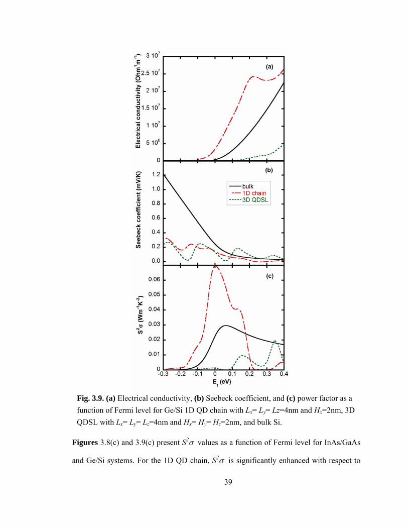
39
Figures 3.8(c) and 3.9(c) present S2σ values as a function of Fermi level for InAs/GaAs
and Ge/Si systems. For the 1D QD chain, S2σ is significantly enhanced with respect to
Fig. 3.9. (a) Electrical conductivity, (b) Seebeck coefficient, and (c) power factor as a function of Fermi level for Ge/Si 1D QD chain with Lx= Ly= Lz=4nm and Hx=2nm, 3D QDSL with Lx= Ly= Lz=4nm and Hx= Hy= Hz=2nm, and bulk Si.
40
the 3D ordered QDSL and bulk, due to the higher σ in the 1D QD chain case. For the 3D
QDSL, due to its low σ, S2σ is not enhanced even with respect to the bulk.
As Hi (φ) is decreased (increased), the interaction between neighboring chains
(interwell coupling Δ/4) is enhanced. At a critical Hi, (given by Δ/4 > Γ=ℏ/τ) there is a
transition from localized carrier transport through QD chains to delocalized carrier
transport in all three directions, as shown in Fig. 3.7. In Ref. [23], a 3D ordered QDSL
with carrier transport coupled to all 3 directions through the minibands was likewise
investigated numerically. In both 3D cases (here and Ref. [23]), insignificant increases in
the S2σ with respect to the maximum S2σ in the bulk were predicted. For the 1D QD
chains, however, as shown in Figs. 3.8 and 3.9, S2σ is predicted to be much higher than
that of either a 3D QDSL or the bulk.
3.7 Summary and Conclusions We have investigated the thermoelectric properties of aligned QD chains and QD chain
nanocomposites in the InAs/GaAs and Ge/Si systems. Using the Schrödinger and
Boltzmann transport equations, we calculated the miniband dispersion and resulting
transport properties S and σ. A comparison of the properties of single QD chains with
those of the corresponding bulk reveals higher S2σ values for both Ge/Si and InAs/GaAs
systems, presumably due to the 1D confinement along the chain length which increases
σ. Additionally, in both cases, S2σ of the QD chains increases with decreasing QD size.
The incorporation of the QD chains into a matrix leads to a reduced S2σ in comparison
with single QD chains, due to parallel conduction through the matrix; however, an
increase in S2σ compared with both the random QD composite and the corresponding
bulk is observed. An increase in thermoelectric power factor by a factor of 3 (1.5) for the
41
InAs/GaAs (Ge/Si) system with respect to bulk is demonstrated. The power factor of a
1D QD chain is shown to be much higher than that of 3D ordered QDSL with similar QD
sizes and spacings. The limitations of our model were assessed in terms of the minimum
(maximum) Hi (φ) for which 1D conduction through the chains occurs without lateral
inter-chain coupling. Overall, we show that the 1D nature of conduction in the minibands
can be exploited to yield a thermoelectric enhancement similar to that predicted for
nanowires and nanowire superlattices, but without the practical difficulties associated
with these structures. This improved thermoelectric performance using aligned QD
chains is a general concept which could be applied to many material systems to yield
high energy conversion efficiencies.
42
Chapter 4
Integrated Thermoelectric Coolers for Mercury
Cadmium Telluride Based Infrared Detectors
4.1 Introduction Mercury cadmium telluride (MCT) is an alloy of semimetal mercury telluride (Eg=-0.01
eV) and semiconductor cadmium telluride (Eg=1.5 eV) [49]. By alloying the two in
various compositions (Hg1-xCdxTe), the bandgap can be controlled between 0 and 1.5 eV.
It has a direct energy gap, high mobility, and low dielectric constant, making it suitable
for many optoelectronic applications such as infrared photodetectors. Specifically, at
x~0.2 the bandgap is matched to long wave infrared (LWIR) light which is detected in
thermal imaging applications such as night vision [49]. MCT has very low electron
effective mass [50], resulting in low scattering rates and very high mobility and electrical
conductivity. The thermal conductivity of bulk MCT is very small [50] (< 4 W/mK at
300K) and decreases with increasing cadmium concentration. However, the density of
electron states is also low, leading to a smaller Seebeck coefficient than many other
semiconductors and poor thermoelectric performance in spite of its high electrical
mobility and low thermal conductivity.
43
Small-barrier [51] and high-barrier [52, 53] quantum well (QW) superlattices
(SLs) have been proposed to improve the ZT of MCT. If MCT with high ZT were
developed, it could be used as a monolithically integrated cooler material for infrared
photodetector pixel elements. Such coolers have potential for dramatically reducing the
pixel operating temperature, leading to greatly reduced noise. Recognizing that the cross-
plane thermoelectric properties of MCT SLs are much better than their in-plane
properties (this direction also being more convenient for monolithic integration with pixel
elements), we concentrate in this chapter on the measurement of cross-plane Seebeck
coefficient and thermal conductivity of small-barrier MCT SLs fabricated by EPIR
Technologies, Inc. (Bolingbrook, IL).
4.2 Cross-plane Seebeck coefficient and thermal
conductivity of small-barrier Hg1-xCdxTe
superlattices Nanostructuring electronic materials can lead to anisotropic thermal and electrical
properties due to quantum confinement effects and scattering at interfaces [4, 31]. 1D
nanostructured materials, such as quantum well superlattices have different thermal and
electrical properties in the direction of growth (cross-plane direction) and in the plane of
growth (inplane direction) [31]. In this chapter, we will concentrate on measurement of
cross-plane thermal conductivity and Seebeck coefficient of small barrier HgCdTe
superlattices.
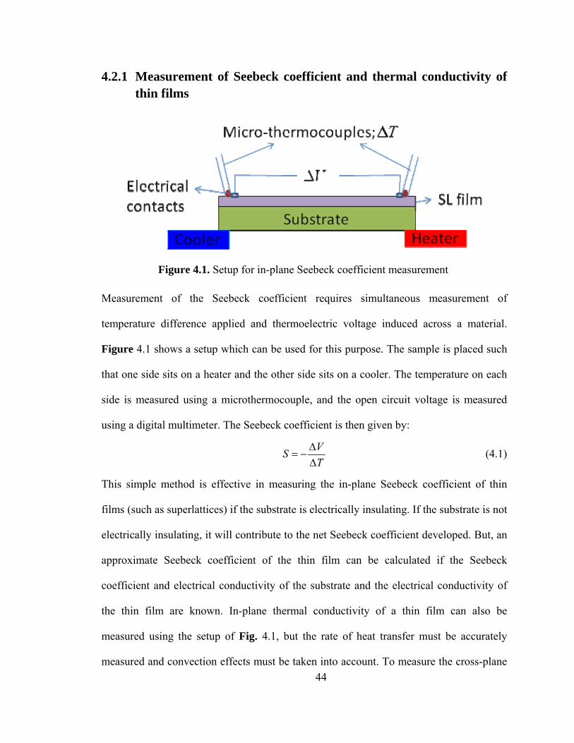
44
4.2.1 Measurement of Seebeck coefficient and thermal conductivity of thin films
Measurement of the Seebeck coefficient requires simultaneous measurement of
temperature difference applied and thermoelectric voltage induced across a material.
Figure 4.1 shows a setup which can be used for this purpose. The sample is placed such
that one side sits on a heater and the other side sits on a cooler. The temperature on each
side is measured using a microthermocouple, and the open circuit voltage is measured
using a digital multimeter. The Seebeck coefficient is then given by:
VST
Δ= −
Δ (4.1)
This simple method is effective in measuring the in-plane Seebeck coefficient of thin
films (such as superlattices) if the substrate is electrically insulating. If the substrate is not
electrically insulating, it will contribute to the net Seebeck coefficient developed. But, an
approximate Seebeck coefficient of the thin film can be calculated if the Seebeck
coefficient and electrical conductivity of the substrate and the electrical conductivity of
the thin film are known. In-plane thermal conductivity of a thin film can also be
measured using the setup of Fig. 4.1, but the rate of heat transfer must be accurately
measured and convection effects must be taken into account. To measure the cross-plane
Figure 4.1. Setup for in-plane Seebeck coefficient measurement
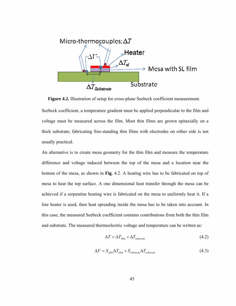
45
Seebeck coefficient, a temperature gradient must be applied perpendicular to the film and
voltage must be measured across the film. Most thin films are grown epitaxially on a
thick substrate; fabricating free-standing thin films with electrodes on either side is not
usually practical.
An alternative is to create mesa geometry for the thin film and measure the temperature
difference and voltage induced between the top of the mesa and a location near the
bottom of the mesa, as shown in Fig. 4.2. A heating wire has to be fabricated on top of
mesa to heat the top surface. A one dimensional heat transfer through the mesa can be
achieved if a serpentine heating wire is fabricated on the mesa to uniformly heat it. If a
line heater is used, then heat spreading inside the mesa has to be taken into account. In
this case, the measured Seebeck coefficient contains contributions from both the thin film
and substrate. The measured thermoelectric voltage and temperature can be written as:
film substrateT T TΔ = Δ + Δ (4.2)
film film substrate substrateV S T S TΔ = Δ + Δ (4.3)
Figure 4.2. Illustration of setup for cross-plane Seebeck coefficient measurement.
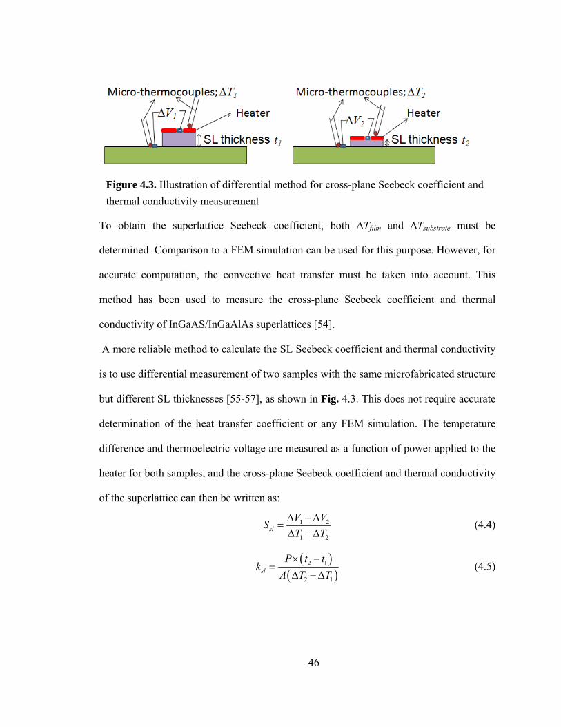
46
To obtain the superlattice Seebeck coefficient, both ΔTfilm and ΔTsubstrate must be
determined. Comparison to a FEM simulation can be used for this purpose. However, for
accurate computation, the convective heat transfer must be taken into account. This
method has been used to measure the cross-plane Seebeck coefficient and thermal
conductivity of InGaAS/InGaAlAs superlattices [54].
A more reliable method to calculate the SL Seebeck coefficient and thermal conductivity
is to use differential measurement of two samples with the same microfabricated structure
but different SL thicknesses [55-57], as shown in Fig. 4.3. This does not require accurate
determination of the heat transfer coefficient or any FEM simulation. The temperature
difference and thermoelectric voltage are measured as a function of power applied to the
heater for both samples, and the cross-plane Seebeck coefficient and thermal conductivity
of the superlattice can then be written as:
1 2
1 2sl
V VST T
Δ − Δ=
Δ − Δ (4.4)
( )( )
2 1
2 1sl
P t tk
A T T× −
=Δ − Δ
(4.5)
Figure 4.3. Illustration of differential method for cross-plane Seebeck coefficient and thermal conductivity measurement
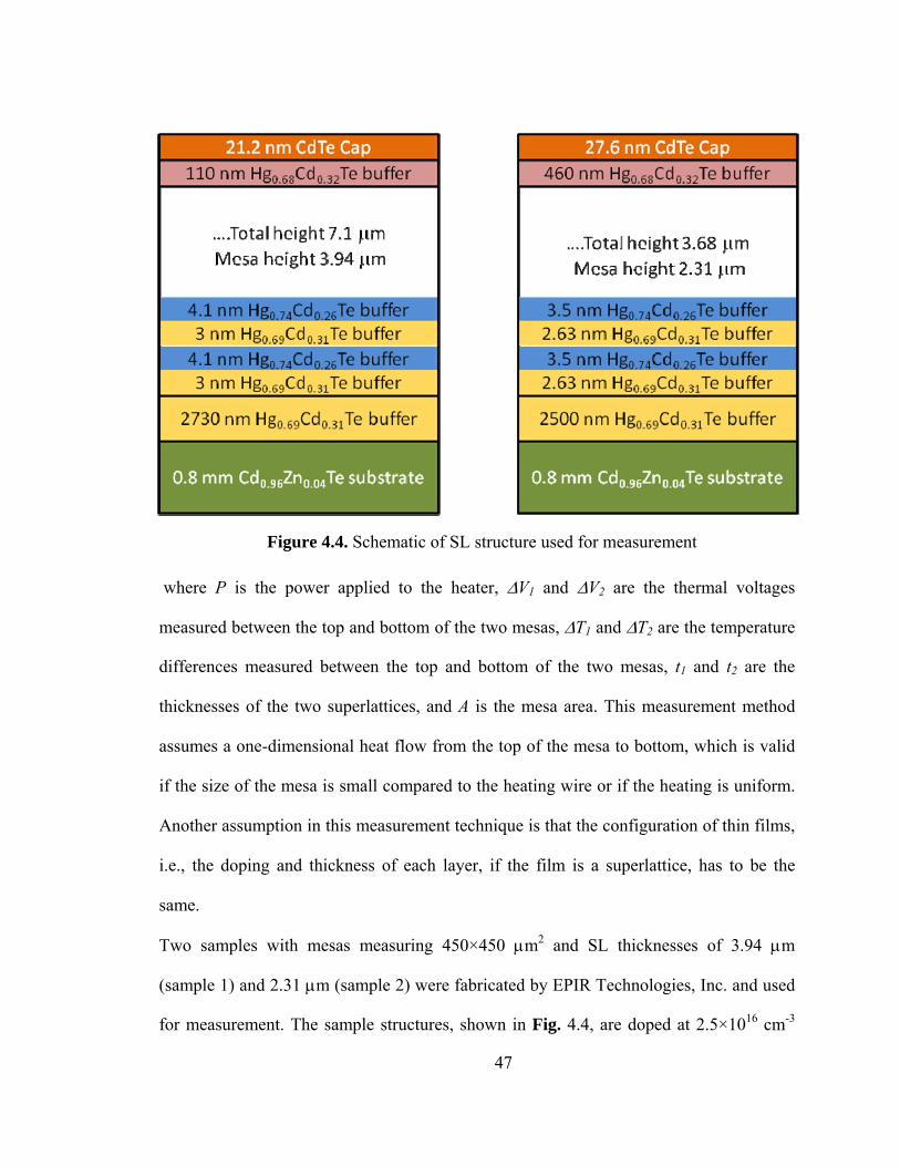
47
where P is the power applied to the heater, ΔV1 and ΔV2 are the thermal voltages
measured between the top and bottom of the two mesas, ΔT1 and ΔT2 are the temperature
differences measured between the top and bottom of the two mesas, t1 and t2 are the
thicknesses of the two superlattices, and A is the mesa area. This measurement method
assumes a one-dimensional heat flow from the top of the mesa to bottom, which is valid
if the size of the mesa is small compared to the heating wire or if the heating is uniform.
Another assumption in this measurement technique is that the configuration of thin films,
i.e., the doping and thickness of each layer, if the film is a superlattice, has to be the
same.
Two samples with mesas measuring 450×450 μm2 and SL thicknesses of 3.94 μm
(sample 1) and 2.31 μm (sample 2) were fabricated by EPIR Technologies, Inc. and used
for measurement. The sample structures, shown in Fig. 4.4, are doped at 2.5×1016 cm-3
Figure 4.4. Schematic of SL structure used for measurement
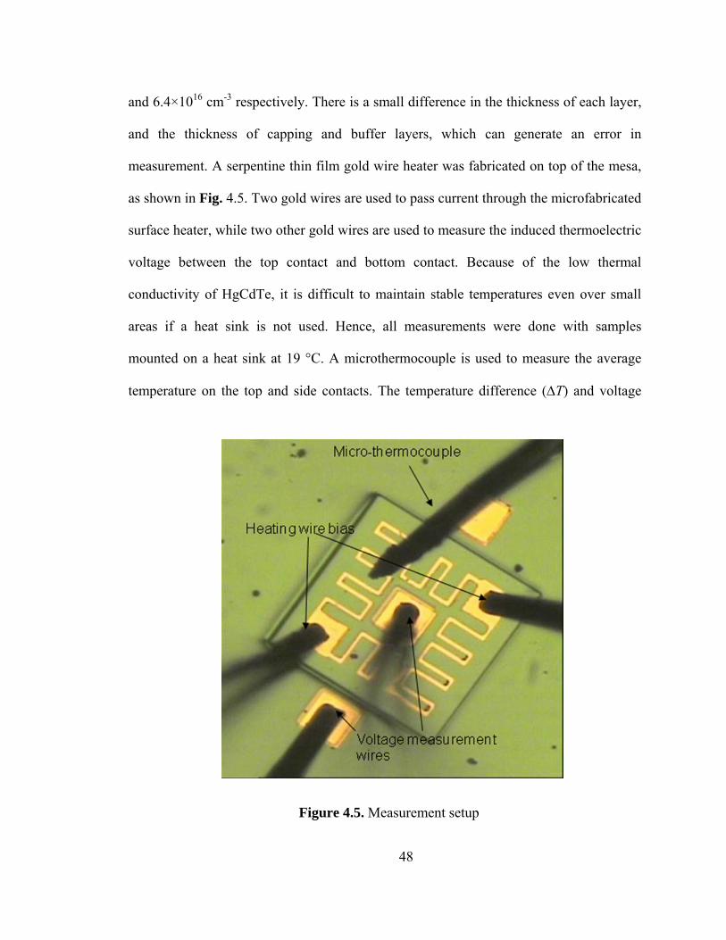
48
and 6.4×1016 cm-3 respectively. There is a small difference in the thickness of each layer,
and the thickness of capping and buffer layers, which can generate an error in
measurement. A serpentine thin film gold wire heater was fabricated on top of the mesa,
as shown in Fig. 4.5. Two gold wires are used to pass current through the microfabricated
surface heater, while two other gold wires are used to measure the induced thermoelectric
voltage between the top contact and bottom contact. Because of the low thermal
conductivity of HgCdTe, it is difficult to maintain stable temperatures even over small
areas if a heat sink is not used. Hence, all measurements were done with samples
mounted on a heat sink at 19 °C. A microthermocouple is used to measure the average
temperature on the top and side contacts. The temperature difference (ΔT) and voltage
Figure 4.5. Measurement setup
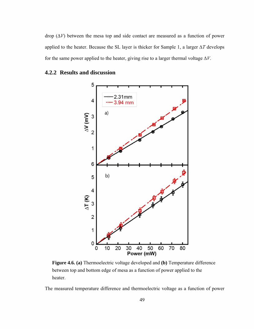
49
drop (ΔV) between the mesa top and side contact are measured as a function of power
applied to the heater. Because the SL layer is thicker for Sample 1, a larger ΔT develops
for the same power applied to the heater, giving rise to a larger thermal voltage ΔV.
4.2.2 Results and discussion
The measured temperature difference and thermoelectric voltage as a function of power
Figure 4.6. (a) Thermoelectric voltage developed and (b) Temperature difference between top and bottom edge of mesa as a function of power applied to the heater.
50
applied to the heater are shown in Figs. 4.6. Recognizing the linear nature of the Seebeck
coefficient reflected in Equation (4.1), linear curves are fit to the ΔT vs. power and ΔV vs.
power curves, yielding the following equations:
( )2 65.66 0.453T PΔ = ± × (4.6)
( )2 48.66 0.48V PΔ = ± × (4.7)
( )1 55.846 0.361T PΔ = ± × (4.8)
( )1 40.54 0.32V PΔ = ± × (4.9)
The slope of ΔT vs. power gives the thermal resistance. The cross-plane thermal
conductivity is then given by:
2 1,2 ,1th th
t tR RkA−
− = (4.10)
where Rth is the thermal resistance, A is the mesa area, t is the SL thickness, and k is the
cross-plane thermal conductivity to be calculated. The Seebeck coefficient was similarly
obtained as the ratio of voltage difference to temperature difference. A thermal
conductivity of 0.82±0.07 W/mK and Seebeck coefficient of 811±150 μV/K were
measured. Although the error in individual measurement is small (0.2 K for ΔT and 0.02
mV for ΔV), this error is amplified when taking the difference ΔT or ΔV between the
samples because of very small difference in thickness between the samples. Hall
measurements were used to measure the resistivity of a sample with superlattice
configuration of 4.1 nm Hg0.74Cd0.26Te/3.5 nm Hg0.68Cd0.32Te and doping of 3.03×10¹⁶
cm-3. These measurements were done at EPIR Technologies, Inc. (Bolingbrook, IL) and a
resistivity of 0.017 Ω.cm was obtained. From this value of resistvity, ZT is calculated to
be 1.43 as compared to a maximum ZT of 0.33 for bulk Hg1-xCdxTe with 0<x<0.3 and
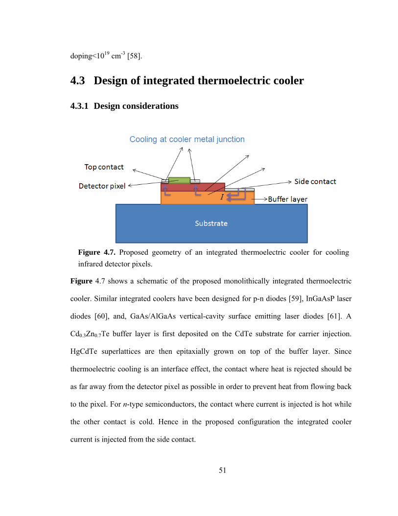
51
doping<1019 cm-3 [58].
4.3 Design of integrated thermoelectric cooler
4.3.1 Design considerations
Figure 4.7 shows a schematic of the proposed monolithically integrated thermoelectric
cooler. Similar integrated coolers have been designed for p-n diodes [59], InGaAsP laser
diodes [60], and, GaAs/AlGaAs vertical-cavity surface emitting laser diodes [61]. A
Cd0.3Zn0.7Te buffer layer is first deposited on the CdTe substrate for carrier injection.
HgCdTe superlattices are then epitaxially grown on top of the buffer layer. Since
thermoelectric cooling is an interface effect, the contact where heat is rejected should be
as far away from the detector pixel as possible in order to prevent heat from flowing back
to the pixel. For n-type semiconductors, the contact where current is injected is hot while
the other contact is cold. Hence in the proposed configuration the integrated cooler
current is injected from the side contact.
Figure 4.7. Proposed geometry of an integrated thermoelectric cooler for cooling infrared detector pixels.
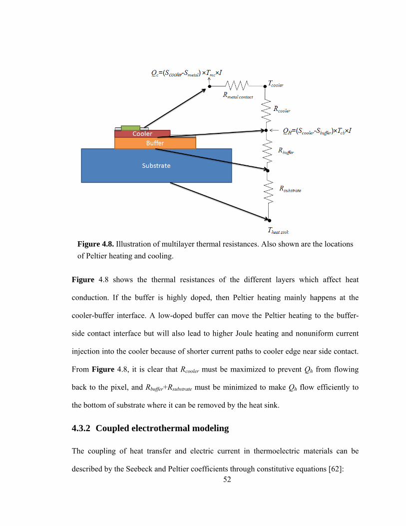
52
Figure 4.8 shows the thermal resistances of the different layers which affect heat
conduction. If the buffer is highly doped, then Peltier heating mainly happens at the
cooler-buffer interface. A low-doped buffer can move the Peltier heating to the buffer-
side contact interface but will also lead to higher Joule heating and nonuniform current
injection into the cooler because of shorter current paths to cooler edge near side contact.
From Figure 4.8, it is clear that Rcooler must be maximized to prevent Qh from flowing
back to the pixel, and Rbuffer+Rsubstrate must be minimized to make Qh flow efficiently to
the bottom of substrate where it can be removed by the heat sink.
4.3.2 Coupled electrothermal modeling
The coupling of heat transfer and electric current in thermoelectric materials can be
described by the Seebeck and Peltier coefficients through constitutive equations [62]:
Figure 4.8. Illustration of multilayer thermal resistances. Also shown are the locations of Peltier heating and cooling.
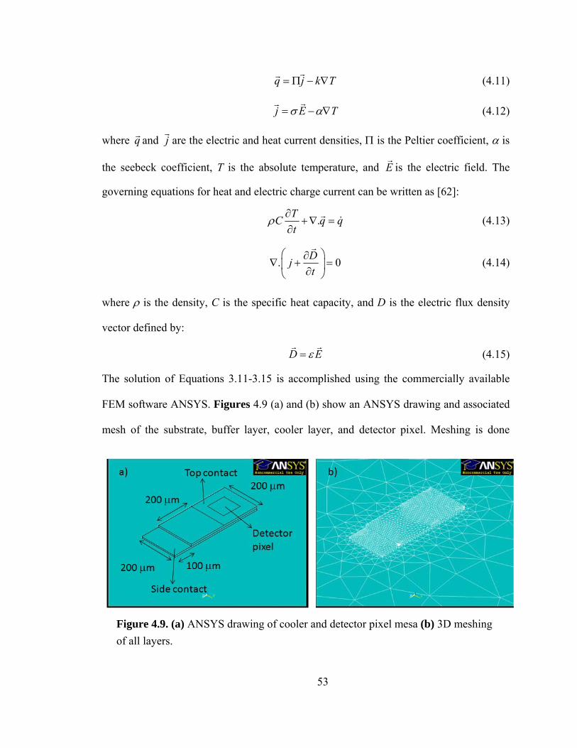
53
q j k T= Π − ∇rr (4.11)
j E Tσ α= − ∇rr
(4.12)
where qr and jr
are the electric and heat current densities, Π is the Peltier coefficient, α is
the seebeck coefficient, T is the absolute temperature, and Er
is the electric field. The
governing equations for heat and electric charge current can be written as [62]:
.TC q qt
ρ ∂+ ∇ =
∂r
& (4.13)
. 0Djt
⎛ ⎞∂∇ + =⎜ ⎟∂⎝ ⎠
r
(4.14)
where ρ is the density, C is the specific heat capacity, and D is the electric flux density
vector defined by:
D Eε=r r
(4.15)
The solution of Equations 3.11-3.15 is accomplished using the commercially available
FEM software ANSYS. Figures 4.9 (a) and (b) show an ANSYS drawing and associated
mesh of the substrate, buffer layer, cooler layer, and detector pixel. Meshing is done
Figure 4.9. (a) ANSYS drawing of cooler and detector pixel mesa (b) 3D meshing of all layers.
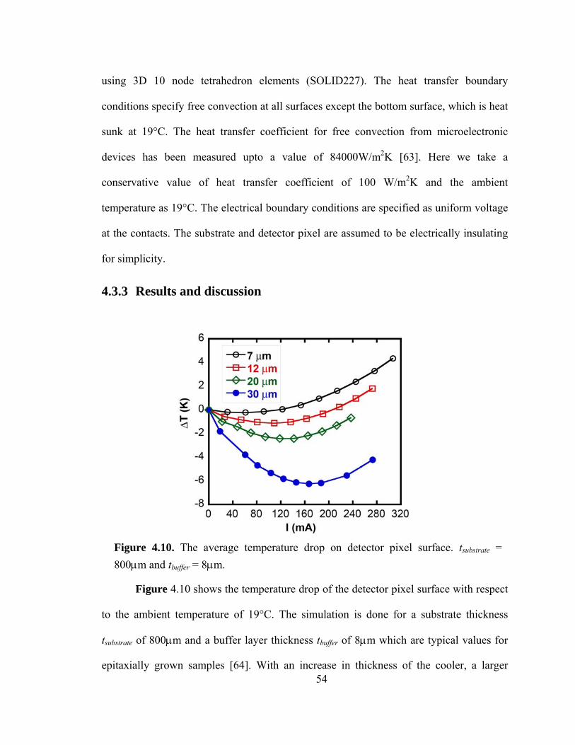
54
using 3D 10 node tetrahedron elements (SOLID227). The heat transfer boundary
conditions specify free convection at all surfaces except the bottom surface, which is heat
sunk at 19°C. The heat transfer coefficient for free convection from microelectronic
devices has been measured upto a value of 84000W/m2K [63]. Here we take a
conservative value of heat transfer coefficient of 100 W/m2K and the ambient
temperature as 19°C. The electrical boundary conditions are specified as uniform voltage
at the contacts. The substrate and detector pixel are assumed to be electrically insulating
for simplicity.
4.3.3 Results and discussion
Figure 4.10 shows the temperature drop of the detector pixel surface with respect
to the ambient temperature of 19°C. The simulation is done for a substrate thickness
tsubstrate of 800μm and a buffer layer thickness tbuffer of 8μm which are typical values for
epitaxially grown samples [64]. With an increase in thickness of the cooler, a larger
Figure 4.10. The average temperature drop on detector pixel surface. tsubstrate = 800μm and tbuffer = 8μm.
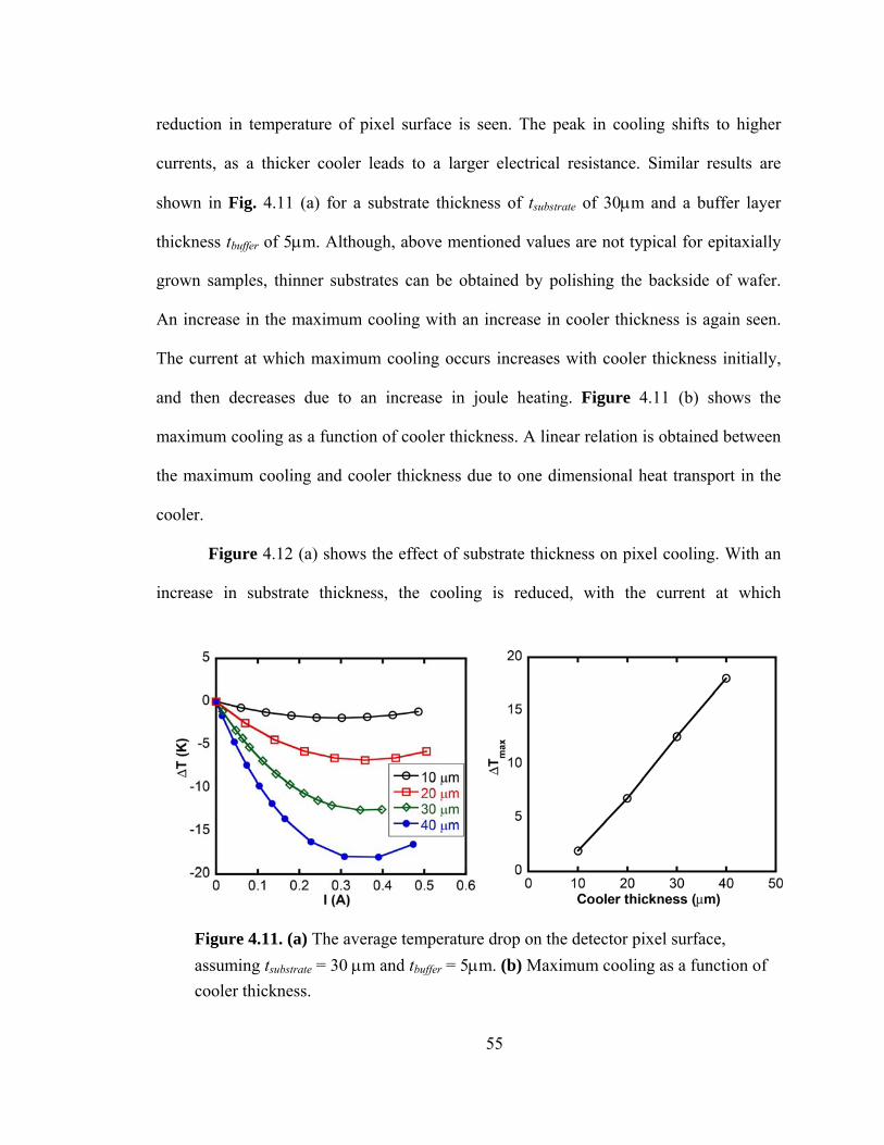
55
reduction in temperature of pixel surface is seen. The peak in cooling shifts to higher
currents, as a thicker cooler leads to a larger electrical resistance. Similar results are
shown in Fig. 4.11 (a) for a substrate thickness of tsubstrate of 30μm and a buffer layer
thickness tbuffer of 5μm. Although, above mentioned values are not typical for epitaxially
grown samples, thinner substrates can be obtained by polishing the backside of wafer.
An increase in the maximum cooling with an increase in cooler thickness is again seen.
The current at which maximum cooling occurs increases with cooler thickness initially,
and then decreases due to an increase in joule heating. Figure 4.11 (b) shows the
maximum cooling as a function of cooler thickness. A linear relation is obtained between
the maximum cooling and cooler thickness due to one dimensional heat transport in the
cooler.
Figure 4.12 (a) shows the effect of substrate thickness on pixel cooling. With an
increase in substrate thickness, the cooling is reduced, with the current at which
Figure 4.11. (a) The average temperature drop on the detector pixel surface, assuming tsubstrate = 30 μm and tbuffer = 5μm. (b) Maximum cooling as a function of cooler thickness.
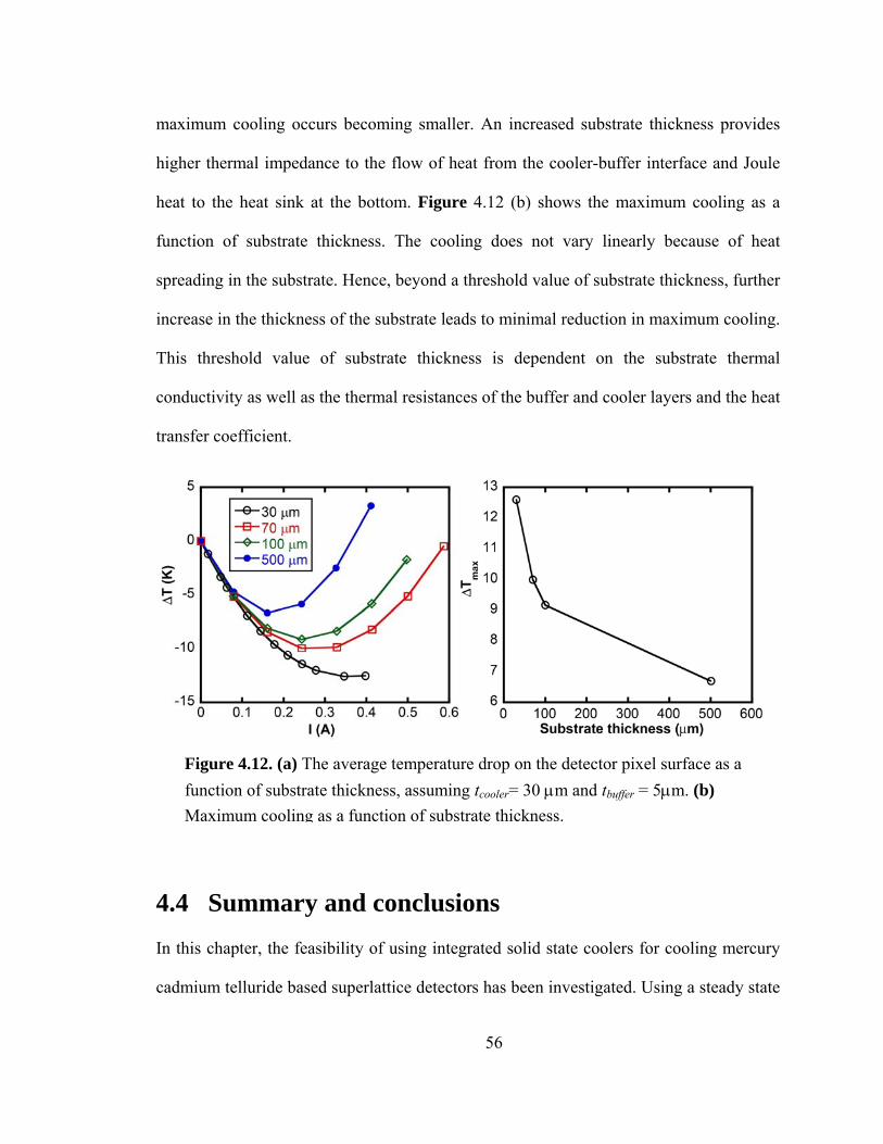
56
maximum cooling occurs becoming smaller. An increased substrate thickness provides
higher thermal impedance to the flow of heat from the cooler-buffer interface and Joule
heat to the heat sink at the bottom. Figure 4.12 (b) shows the maximum cooling as a
function of substrate thickness. The cooling does not vary linearly because of heat
spreading in the substrate. Hence, beyond a threshold value of substrate thickness, further
increase in the thickness of the substrate leads to minimal reduction in maximum cooling.
This threshold value of substrate thickness is dependent on the substrate thermal
conductivity as well as the thermal resistances of the buffer and cooler layers and the heat
transfer coefficient.
4.4 Summary and conclusions In this chapter, the feasibility of using integrated solid state coolers for cooling mercury
cadmium telluride based superlattice detectors has been investigated. Using a steady state
Figure 4.12. (a) The average temperature drop on the detector pixel surface as a function of substrate thickness, assuming tcooler= 30 μm and tbuffer = 5μm. (b) Maximum cooling as a function of substrate thickness.
57
differential measurement, the cross-plane Seebeck coefficient and thermal conductivity of
small barrier HgCdTe superlattices were measured, finding a Seebeck coefficient of
811±150 μV/K and a thermal conductivity of 0.82±0.07 W/mK. Assuming an electrical
resistivity of 0.017 Ω·cm (obtained from Hall measurements), a ZT value of 1.43 is
obtained, as compared to ZT of 0.33 for bulk Hg1-xCdxTe with 0<x<0.3 and doping<1019
cm-3. This increase in ZT is attributed to an increase in the Seebeck coefficient as well as
a decrease in thermal conductivity. Although a ZT of 1.43 is still small for solid state heat
engines or heat pumps to compete with mechanical heat engines and heat pumps, it
shows a promising trend of using nanostructed HgCdTe superlattices for high efficiency
thermoelectrics.
Using the obtained values of Seebeck coefficient and thermal conductivity, we use FEM
simulation to design a thermoelectric cooler monolithically integrated with an infrared
detector pixel. An integrated cooler can help in reducing local hot spots, and effectively
pumping heat from active device area in a chip, such as infrared detector pixel in a focal
plane array, to the parts of chip which are not utilized in active devices such as substrate.
We find a general trend of higher cooling with thinner substrates and thicker cooler
layers. The cooling on pixel surface increases linearly with cooler thickness
demonstrating a one dimensional heat transfer in the cooler. With an increase in thickness
of substrate, the cooling decrease in a non linear fashion because of heat spreading in the
substrate.
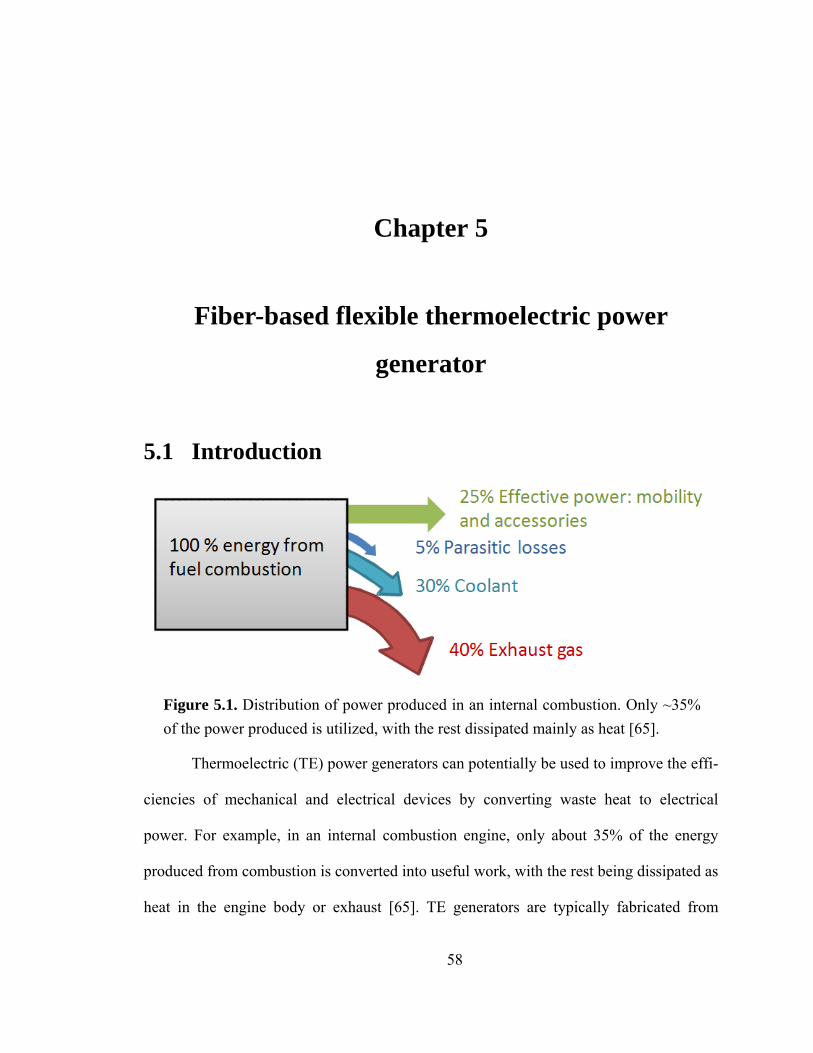
58
Chapter 5
Fiber-based flexible thermoelectric power
generator
5.1 Introduction
Thermoelectric (TE) power generators can potentially be used to improve the effi-
ciencies of mechanical and electrical devices by converting waste heat to electrical
power. For example, in an internal combustion engine, only about 35% of the energy
produced from combustion is converted into useful work, with the rest being dissipated as
heat in the engine body or exhaust [65]. TE generators are typically fabricated from
Figure 5.1. Distribution of power produced in an internal combustion. Only ~35% of the power produced is utilized, with the rest dissipated mainly as heat [65].
59
crystalline semiconductors such as Bi2Te3 or SiGe, making them rigid and unsuitable for
covering large areas or arbitrary shapes that are commonly encountered in waste heat
recovery applications. In order to improve thermal contact to heat sources of arbitrary
geometry, it is desirable to produce thermoelectric generators that can conform easily to a
surface. However, thermoelectric devices based on flexible materials such as organic
semiconductors have proven impractical to date due to low ZT stemming from low
electrical carrier mobility [66]. Another idea is to embed discrete miniature TE chips in a
flexible matrix; however, such systems are not easy or inexpensive to manufacture and
may be hampered by their reliability [20].
A more desirable configuration is one in which intrinsically flexible thermoelec-
tric devices are fabricated in an inexpensive reel-to-reel process. Flexible photovoltaic
cells [67] and organic light emitting diodes (OLEDs) [68] have been fabricated by
depositing thin films on flexible substrates or fibers [69, 70]. In addition, miniaturization
of energy conversion devices is being pursued to operate low power electronics using
readily available energy sources such as human body heat [71] or heel strikes during
walking [71].
Previous work in flexible thermoelectric power generators has involved fabrica-
tion of multiple thermocouple junctions on flexible planar substrates. Itoigawa et al. [72]
used a wavy polyimide sheet with junctions at the top and bottom of the sheet to build a
flexible thermopile. Sato et al [73] used a combination of copper and polyimide sheets as
a flexible substrate to create an in-plane temperature gradient from a cross-plane heat
flux. These techniques require photolithography and precision machining, however, and
their flexibility is limited to a single plane and constrained by the thickness of the
substrate. Here we demonstrate a flexible thermoelectric generator based on thin-film
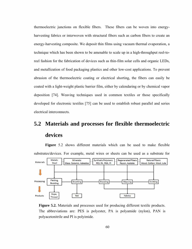
60
thermoelectric junctions on flexible fibers. These fibers can be woven into energy-
harvesting fabrics or interwoven with structural fibers such as carbon fibers to create an
energy-harvesting composite. We deposit thin films using vacuum thermal evaporation, a
technique which has been shown to be amenable to scale up in a high-throughput reel-to-
reel fashion for the fabrication of devices such as thin-film solar cells and organic LEDs,
and metallization of food packaging plastics and other low-cost applications. To prevent
abrasion of the thermoelectric coating or electrical shorting, the fibers can easily be
coated with a light-weight plastic barrier film, either by calendaring or by chemical vapor
deposition [74]. Weaving techniques used in common textiles or those specifically
developed for electronic textiles [75] can be used to establish robust parallel and series
electrical interconnects.
5.2 Materials and processes for flexible thermoelectric
devices Figure 5.2 shows different materials which can be used to make flexible
substrates/devices. For example, metal wires or sheets can be used as a substrate for
Figure 5.2. Materials and processes used for producing different textile products. The abbreviations are: PES is polyester, PA is polyamide (nylon), PAN is polyacetonitrile and PI is polyimide.
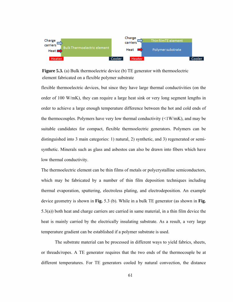
61
flexible thermoelectric devices, but since they have large thermal conductivities (on the
order of 100 W/mK), they can require a large heat sink or very long segment lengths in
order to achieve a large enough temperature difference between the hot and cold ends of
the thermocouples. Polymers have very low thermal conductivity (<1W/mK), and may be
suitable candidates for compact, flexible thermoelectric generators. Polymers can be
distinguished into 3 main categories: 1) natural, 2) synthetic, and 3) regenerated or semi-
synthetic. Minerals such as glass and asbestos can also be drawn into fibers which have
low thermal conductivity.
The thermoelectric element can be thin films of metals or polycrystalline semiconductors,
which may be fabricated by a number of thin film deposition techniques including
thermal evaporation, sputtering, electroless plating, and electrodeposition. An example
device geometry is shown in Fig. 5.3 (b). While in a bulk TE generator (as shown in Fig.
5.3(a)) both heat and charge carriers are carried in same material, in a thin film device the
heat is mainly carried by the electrically insulating substrate. As a result, a very large
temperature gradient can be established if a polymer substrate is used.
The substrate material can be processed in different ways to yield fabrics, sheets,
or threads/ropes. A TE generator requires that the two ends of the thermocouple be at
different temperatures. For TE generators cooled by natural convection, the distance
Figure 5.3. (a) Bulk thermoelectric device (b) TE generator with thermoelectric element fabricated on a flexible polymer substrate
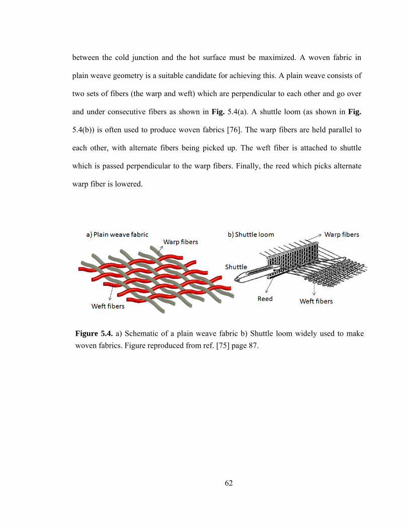
62
between the cold junction and the hot surface must be maximized. A woven fabric in
plain weave geometry is a suitable candidate for achieving this. A plain weave consists of
two sets of fibers (the warp and weft) which are perpendicular to each other and go over
and under consecutive fibers as shown in Fig. 5.4(a). A shuttle loom (as shown in Fig.
5.4(b)) is often used to produce woven fabrics [76]. The warp fibers are held parallel to
each other, with alternate fibers being picked up. The weft fiber is attached to shuttle
which is passed perpendicular to the warp fibers. Finally, the reed which picks alternate
warp fiber is lowered.
Figure 5.4. a) Schematic of a plain weave fabric b) Shuttle loom widely used to make woven fabrics. Figure reproduced from ref. [75] page 87.
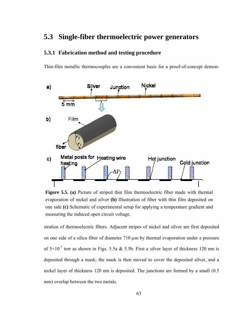
63
5.3 Single-fiber thermoelectric power generators
5.3.1 Fabrication method and testing procedure
Thin-film metallic thermocouples are a convenient basis for a proof-of-concept demon-
stration of thermoelectric fibers. Adjacent stripes of nickel and silver are first deposited
on one side of a silica fiber of diameter 710 μm by thermal evaporation under a pressure
of 5×10⁻⁷ torr as shown in Figs. 5.5a & 5.5b. First a silver layer of thickness 120 nm is
deposited through a mask; the mask is then moved to cover the deposited silver, and a
nickel layer of thickness 120 nm is deposited. The junctions are formed by a small (0.5
mm) overlap between the two metals.
Figure 5.5. (a) Picture of striped thin film thermoelectric fiber made with thermal evaporation of nickel and silver (b) Illustration of fiber with thin film deposited on one side (c) Schematic of experimental setup for applying a temperature gradient and measuring the induced open circuit voltage.
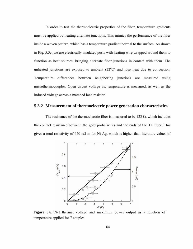
64
In order to test the thermoelectric properties of the fiber, temperature gradients
must be applied by heating alternate junctions. This mimics the performance of the fiber
inside a woven pattern, which has a temperature gradient normal to the surface. As shown
in Fig. 5.5c, we use electrically insulated posts with heating wire wrapped around them to
function as heat sources, bringing alternate fiber junctions in contact with them. The
unheated junctions are exposed to ambient (22oC) and lose heat due to convection.
Temperature differences between neighboring junctions are measured using
microthermocouples. Open circuit voltage vs. temperature is measured, as well as the
induced voltage across a matched load resistor.
5.3.2 Measurement of thermoelectric power generation characteristics
The resistance of the thermoelectric fiber is measured to be 123 Ω, which includes
the contact resistance between the gold probe wires and the ends of the TE fiber. This
gives a total resistivity of 470 nΩ m for Ni-Ag, which is higher than literature values of
Figure 5.6. Net thermal voltage and maximum power output as a function of temperature applied for 7 couples.
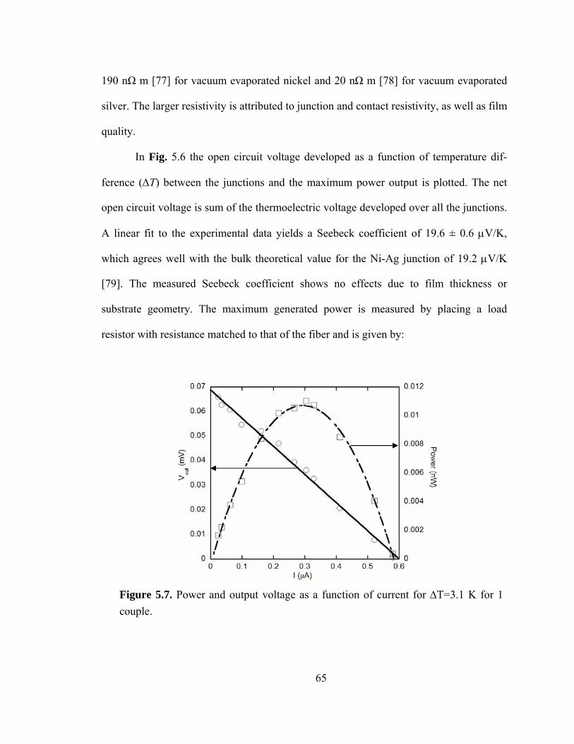
65
190 nΩ m [77] for vacuum evaporated nickel and 20 nΩ m [78] for vacuum evaporated
silver. The larger resistivity is attributed to junction and contact resistivity, as well as film
quality.
In Fig. 5.6 the open circuit voltage developed as a function of temperature dif-
ference (ΔT) between the junctions and the maximum power output is plotted. The net
open circuit voltage is sum of the thermoelectric voltage developed over all the junctions.
A linear fit to the experimental data yields a Seebeck coefficient of 19.6 ± 0.6 μV/K,
which agrees well with the bulk theoretical value for the Ni-Ag junction of 19.2 μV/K
[79]. The measured Seebeck coefficient shows no effects due to film thickness or
substrate geometry. The maximum generated power is measured by placing a load
resistor with resistance matched to that of the fiber and is given by:
Figure 5.7. Power and output voltage as a function of current for ΔT=3.1 K for 1 couple.
66
2 2 2
max 4 f
n S TPRΔ
= (5.1)
where Pmax is the maximum power output, S is the net Seebeck coefficient of each junc-
tion, n is the number of thermocouples, and Rf is the total electrical resistance of the fiber,
which can be written as:
pef
e p
R nlA A
ρρ⎛ ⎞= +⎜ ⎟⎜ ⎟
⎝ ⎠ (5.2)
where ρe and ρp are the electrical resistivity of the n and p segments and Ae and Ap are the
respective cross-sectional areas. The maximum power increases as the square of the
temperature difference applied, which is seen in the experimental data. The internal
resistance of the fiber and the combined Seebeck coefficient of the junction also affect
the power output. Figure 5.7 plots the voltage and power versus the current produced by
a single thermocouple for a constant ΔT = 3.1 K. At a constant ΔT, the fiber acts as a
constant voltage source for which the maximum current is given by the short circuit
current. With an increase in load resistance, the current decreases but the output voltage
increases; hence there is a maximum in the power output at a load resistance that is
matched to the resistance of fiber. Increasing the number of thermocouples shifts the line
upward, but the slope of the Vout versus I curve will remain constant for same load
resistance. Increasing the number of thermocouples will increase the maximum output
voltage (ΔVOC), as well as the slope of the graph (i.e. fiber resistance, Rf). As Equation
(5.1) indicates, the power will increase linearly with the number of couples.
67
5.3.3 Optimization of material parameters for maximizing power generation
In thermoelectric power generators ΔT is often a fixed parameter, given for
example by the wall temperature of the heat source and the lowest heat sink temperature
accessible via convective cooling. In the case of constant ΔT, the power simply scales as
1/l with increasing segment length l, due to an increase in the electrical resistance [80].
Taking into account the effect of contact resistance, an optimization of power can be
obtained [81, 82]. For fiber-based flexible thermoelectric power generators, one practical
configuration would involve a woven thermoelectric fabric wrapped around a hot object,
experiencing convective cooling on the opposite side. Under these boundary conditions,
both ΔT and resistance can change with segment length, and an optimization in power
output can also be obtained. To investigate the optimization conditions for power output,
a simple fin heat transfer equation is used to calculate the temperature difference between
the hot and cold junctions. The thermal resistances of the thin film and fiber substrate are
given by [83]:
( ), 2 2
2 1th film
film
lRr r kπ
=−
(5.3)
, 21
th fiberfiber
lRr kπ
= (5.4)
where r2 and r1 are the outer and inner diameters as shown in Fig. 5.5, kfiber is the thermal
conductivity of the fiber, and kfilm is the thermal conductivity of the thin film. For the
silica fiber, the thermal conductivity is 1.2 W/mK, and the thermal resistance of both
metal films is calculated to be at least 9 times larger than the thermal resistance of the
fiber; hence heat transfer through the film is neglected. If thicker films of metals were to
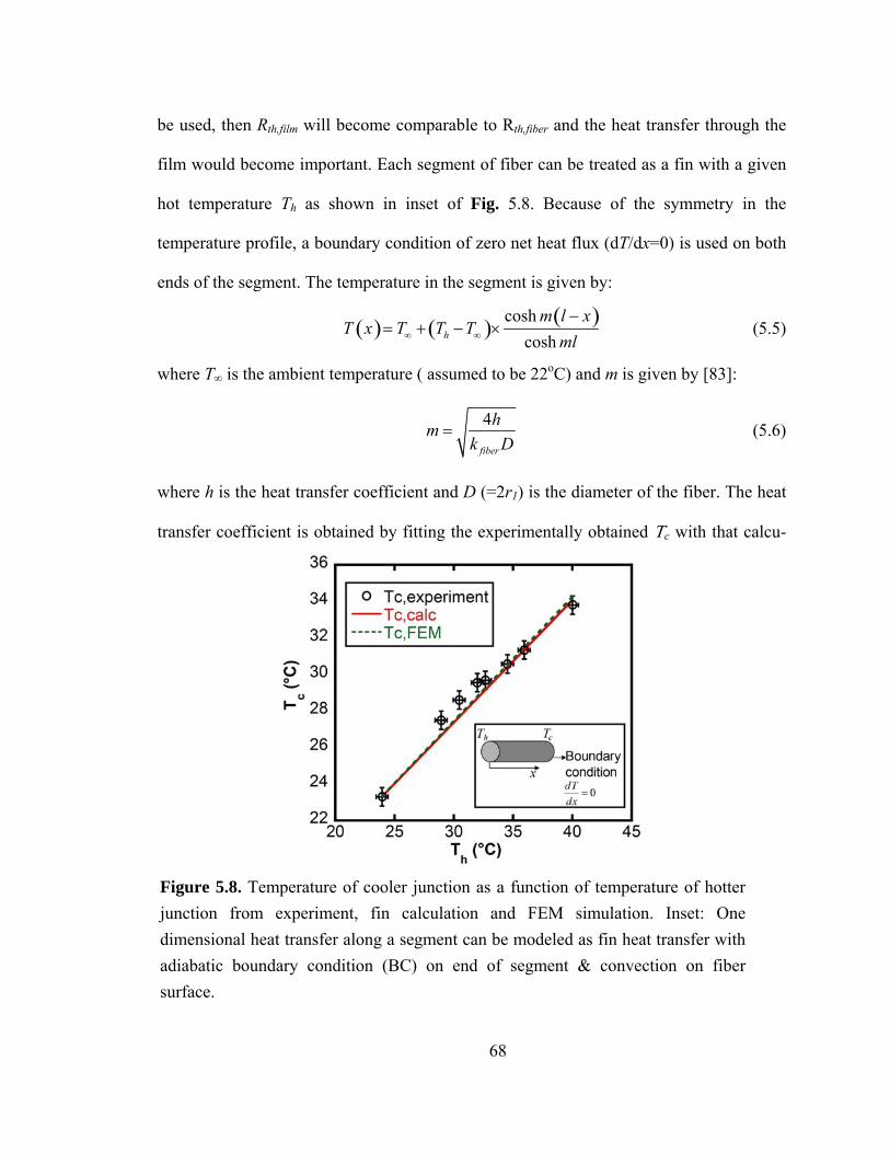
68
be used, then Rth,film will become comparable to Rth,fiber and the heat transfer through the
film would become important. Each segment of fiber can be treated as a fin with a given
hot temperature Th as shown in inset of Fig. 5.8. Because of the symmetry in the
temperature profile, a boundary condition of zero net heat flux (dT/dx=0) is used on both
ends of the segment. The temperature in the segment is given by:
( ) ( ) ( )coshcoshh
m l xT x T T T
ml∞ ∞
−= + − × (5.5)
where T∞ is the ambient temperature ( assumed to be 22oC) and m is given by [83]:
4
fiber
hmk D
= (5.6)
where h is the heat transfer coefficient and D (=2r1) is the diameter of the fiber. The heat
transfer coefficient is obtained by fitting the experimentally obtained Τc with that calcu-
Figure 5.8. Temperature of cooler junction as a function of temperature of hotter junction from experiment, fin calculation and FEM simulation. Inset: One dimensional heat transfer along a segment can be modeled as fin heat transfer with adiabatic boundary condition (BC) on end of segment & convection on fiber surface.
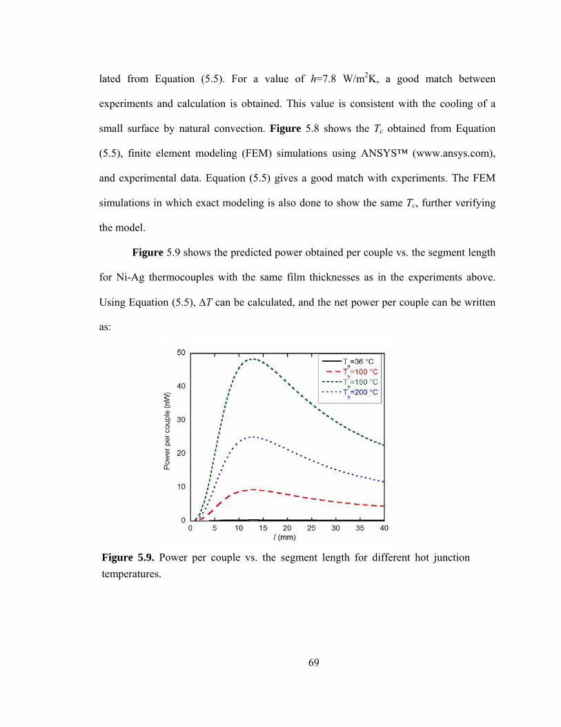
69
lated from Equation (5.5). For a value of h=7.8 W/m2K, a good match between
experiments and calculation is obtained. This value is consistent with the cooling of a
small surface by natural convection. Figure 5.8 shows the Tc obtained from Equation
(5.5), finite element modeling (FEM) simulations using ANSYS™ (www.ansys.com),
and experimental data. Equation (5.5) gives a good match with experiments. The FEM
simulations in which exact modeling is also done to show the same Tc, further verifying
the model.
Figure 5.9 shows the predicted power obtained per couple vs. the segment length
for Ni-Ag thermocouples with the same film thicknesses as in the experiments above.
Using Equation (5.5), ΔT can be calculated, and the net power per couple can be written
as:
Figure 5.9. Power per couple vs. the segment length for different hot junction temperatures.
70
( )( )
2
22 118 4cosh
h
e p
fiber
S T T t DPl h l
k D
πρ ρ
∞
⎛ ⎞⎜ ⎟
− ⎜ ⎟= × −⎜ ⎟+ ⎜ ⎟⎜ ⎟⎝ ⎠
(5.7)
where t is the thickness of films. With an increase in segment length, the resistance of
the fiber-based thermoelectric device increases linearly. However, there is also an in-
crease in ΔT, until the maximum ΔT of Th- T∞ is obtained. At short segment lengths, the
increase in ΔT dominates, and there is an increase in power. At large segment lengths, ΔT
saturates at a value of Th-T∞, and the power decreases as 1/l. A maximum power per
couple is obtained by minimizing Equation (5.7) with respect to l, yielding an
optimization condition for a given diameter of fiber:
max4 2.44h lkD
= (5.8)
For the silica fiber having approximately 0.71 mm diameter used in the experiments here,
lmax=13 mm is obtained. Smaller diameter fibers would allow a shorter segment length.
Other controllable parameters include the thickness and composition of the de-
posited thin films. In Fig. 5.10, the effects of depositing materials with high
thermoelectric figure-of-merit (ZT) at different film thicknesses are investigated. Bi2Te3-
Sb2Te3 is a high ZT material, but for thin films the increase in electrical resistance caused
by using a semiconductor material can offset the effect of increased thermopower. The
Seebeck coefficient for Bi2Te3-Sb2Te3 is taken to be 375 μV/K, and the total resistivity is
taken to be 33.5 μΩ·m. These values are based on thermally co-evaporated thin film
measurements with a substrate temperature of 260 °C [84]. Similar values have also been
obtained for Bi2Te3-Sb2Te3 films evaporated on polyimide substrates [85]. For Bi2Te3-
Sb2Te3 thin films having the same thickness as Ni-Ag films, the generated power is
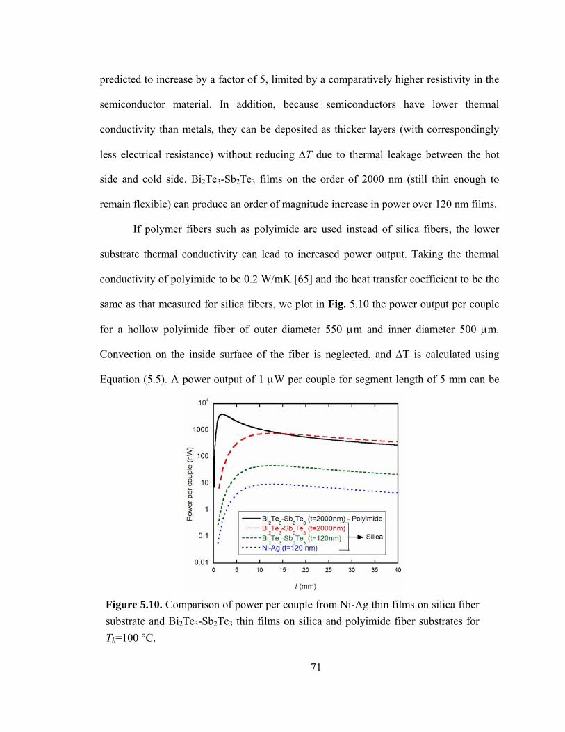
71
predicted to increase by a factor of 5, limited by a comparatively higher resistivity in the
semiconductor material. In addition, because semiconductors have lower thermal
conductivity than metals, they can be deposited as thicker layers (with correspondingly
less electrical resistance) without reducing ΔT due to thermal leakage between the hot
side and cold side. Bi2Te3-Sb2Te3 films on the order of 2000 nm (still thin enough to
remain flexible) can produce an order of magnitude increase in power over 120 nm films.
If polymer fibers such as polyimide are used instead of silica fibers, the lower
substrate thermal conductivity can lead to increased power output. Taking the thermal
conductivity of polyimide to be 0.2 W/mK [65] and the heat transfer coefficient to be the
same as that measured for silica fibers, we plot in Fig. 5.10 the power output per couple
for a hollow polyimide fiber of outer diameter 550 μm and inner diameter 500 μm.
Convection on the inside surface of the fiber is neglected, and ΔT is calculated using
Equation (5.5). A power output of 1 μW per couple for segment length of 5 mm can be
Figure 5.10. Comparison of power per couple from Ni-Ag thin films on silica fiber substrate and Bi2Te3-Sb2Te3 thin films on silica and polyimide fiber substrates for Th=100 °C.
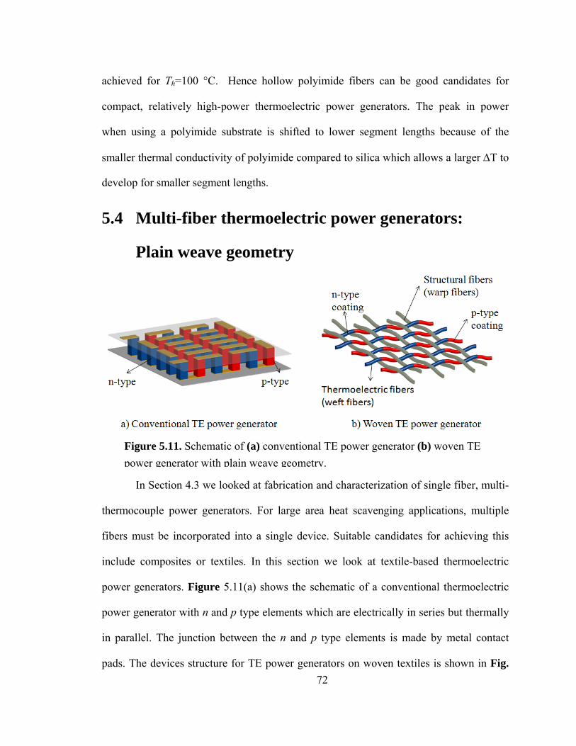
72
achieved for Th=100 °C. Hence hollow polyimide fibers can be good candidates for
compact, relatively high-power thermoelectric power generators. The peak in power
when using a polyimide substrate is shifted to lower segment lengths because of the
smaller thermal conductivity of polyimide compared to silica which allows a larger ΔT to
develop for smaller segment lengths.
5.4 Multi-fiber thermoelectric power generators:
Plain weave geometry
In Section 4.3 we looked at fabrication and characterization of single fiber, multi-
thermocouple power generators. For large area heat scavenging applications, multiple
fibers must be incorporated into a single device. Suitable candidates for achieving this
include composites or textiles. In this section we look at textile-based thermoelectric
power generators. Figure 5.11(a) shows the schematic of a conventional thermoelectric
power generator with n and p type elements which are electrically in series but thermally
in parallel. The junction between the n and p type elements is made by metal contact
pads. The devices structure for TE power generators on woven textiles is shown in Fig.
Figure 5.11. Schematic of (a) conventional TE power generator (b) woven TE power generator with plain weave geometry.
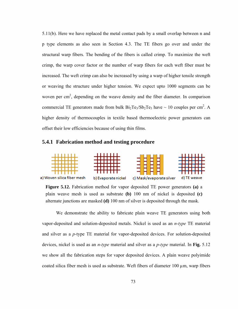
73
5.11(b). Here we have replaced the metal contact pads by a small overlap between n and
p type elements as also seen in Section 4.3. The TE fibers go over and under the
structural warp fibers. The bending of the fibers is called crimp. To maximize the weft
crimp, the warp cover factor or the number of warp fibers for each weft fiber must be
increased. The weft crimp can also be increased by using a warp of higher tensile strength
or weaving the structure under higher tension. We expect upto 1000 segments can be
woven per cm2, depending on the weave density and the fiber diameter. In comparison
commercial TE generators made from bulk Bi2Te3/Sb2Te3 have ~ 10 couples per cm2. A
higher density of thermocouples in textile based thermoelectric power generators can
offset their low efficiencies because of using thin films.
5.4.1 Fabrication method and testing procedure
We demonstrate the ability to fabricate plain weave TE generators using both
vapor-deposited and solution-deposited metals. Nickel is used as an n-type TE material
and silver as a p-type TE material for vapor-deposited devices. For solution-deposited
devices, nickel is used as an n-type material and silver as a p-type material. In Fig. 5.12
we show all the fabrication steps for vapor deposited devices. A plain weave polyimide
coated silica fiber mesh is used as substrate. Weft fibers of diameter 100 μm, warp fibers
Figure 5.12. Fabrication method for vapor deposited TE power generators (a) a plain weave mesh is used as substrate (b) 100 nm of nickel is deposited (c) alternate junctions are masked (d) 100 nm of silver is deposited through the mask.
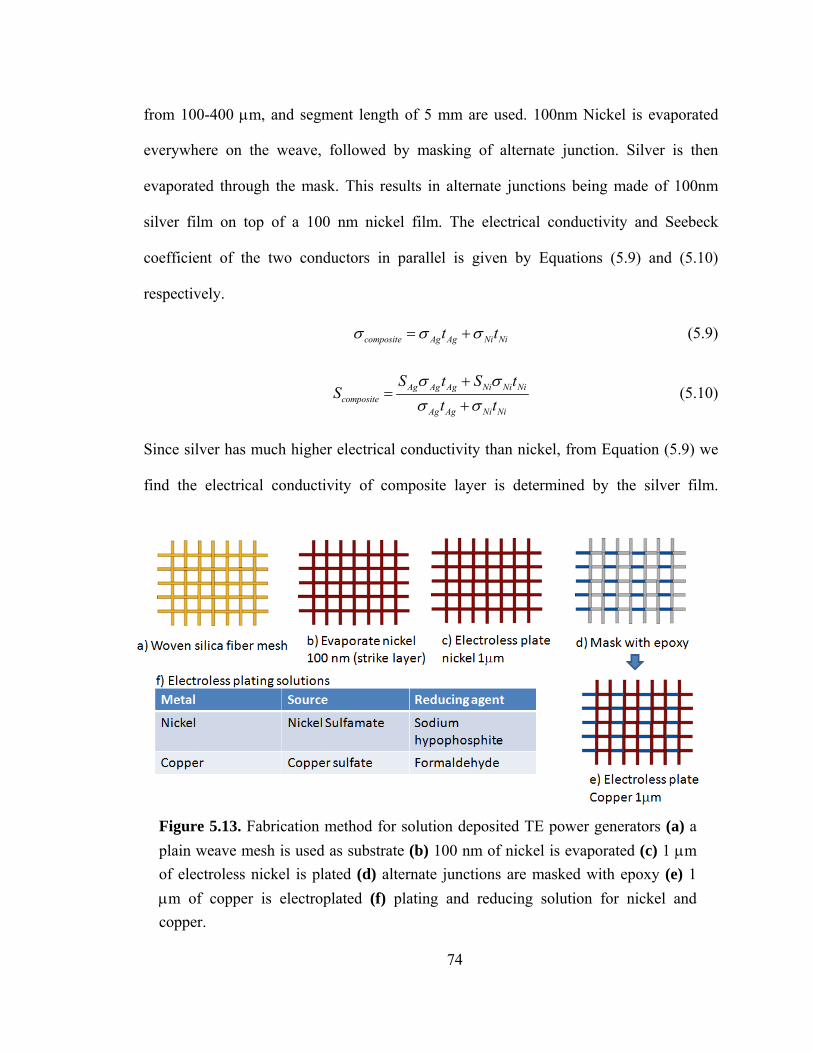
74
from 100-400 μm, and segment length of 5 mm are used. 100nm Nickel is evaporated
everywhere on the weave, followed by masking of alternate junction. Silver is then
evaporated through the mask. This results in alternate junctions being made of 100nm
silver film on top of a 100 nm nickel film. The electrical conductivity and Seebeck
coefficient of the two conductors in parallel is given by Equations (5.9) and (5.10)
respectively.
composite Ag Ag Ni Nit tσ σ σ= + (5.9)
Ag Ag Ag Ni Ni Nicomposite
Ag Ag Ni Ni
S t S tS
t tσ σσ σ
+=
+ (5.10)
Since silver has much higher electrical conductivity than nickel, from Equation (5.9) we
find the electrical conductivity of composite layer is determined by the silver film.
Figure 5.13. Fabrication method for solution deposited TE power generators (a) a plain weave mesh is used as substrate (b) 100 nm of nickel is evaporated (c) 1 μm of electroless nickel is plated (d) alternate junctions are masked with epoxy (e) 1 μm of copper is electroplated (f) plating and reducing solution for nickel and copper.
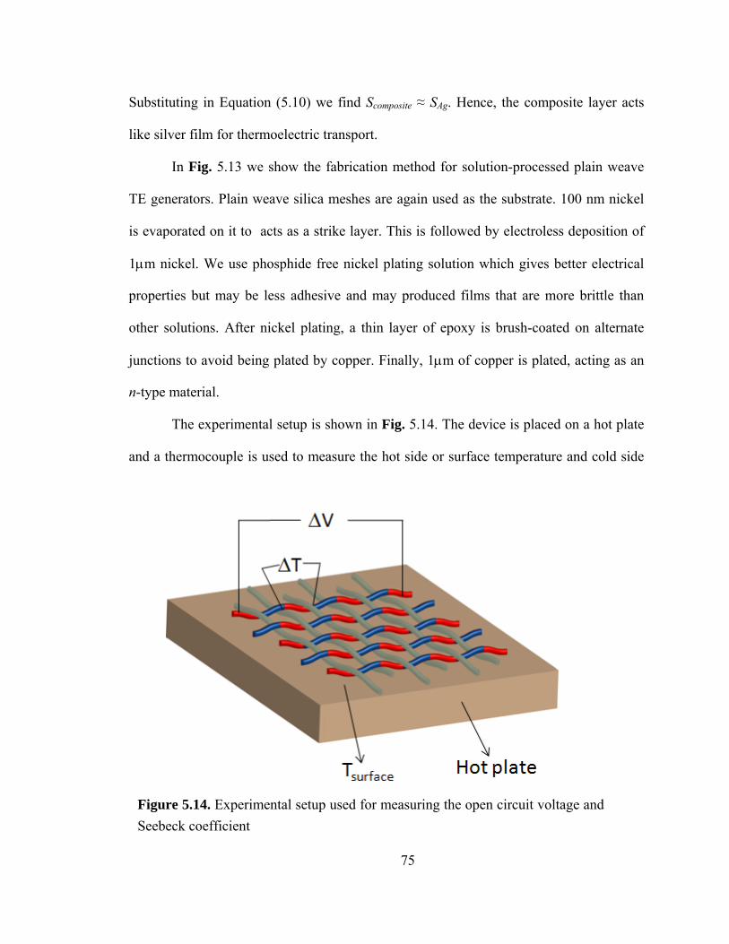
75
Substituting in Equation (5.10) we find Scomposite ≈ SAg. Hence, the composite layer acts
like silver film for thermoelectric transport.
In Fig. 5.13 we show the fabrication method for solution-processed plain weave
TE generators. Plain weave silica meshes are again used as the substrate. 100 nm nickel
is evaporated on it to acts as a strike layer. This is followed by electroless deposition of
1μm nickel. We use phosphide free nickel plating solution which gives better electrical
properties but may be less adhesive and may produced films that are more brittle than
other solutions. After nickel plating, a thin layer of epoxy is brush-coated on alternate
junctions to avoid being plated by copper. Finally, 1μm of copper is plated, acting as an
n-type material.
The experimental setup is shown in Fig. 5.14. The device is placed on a hot plate
and a thermocouple is used to measure the hot side or surface temperature and cold side
Figure 5.14. Experimental setup used for measuring the open circuit voltage and Seebeck coefficient
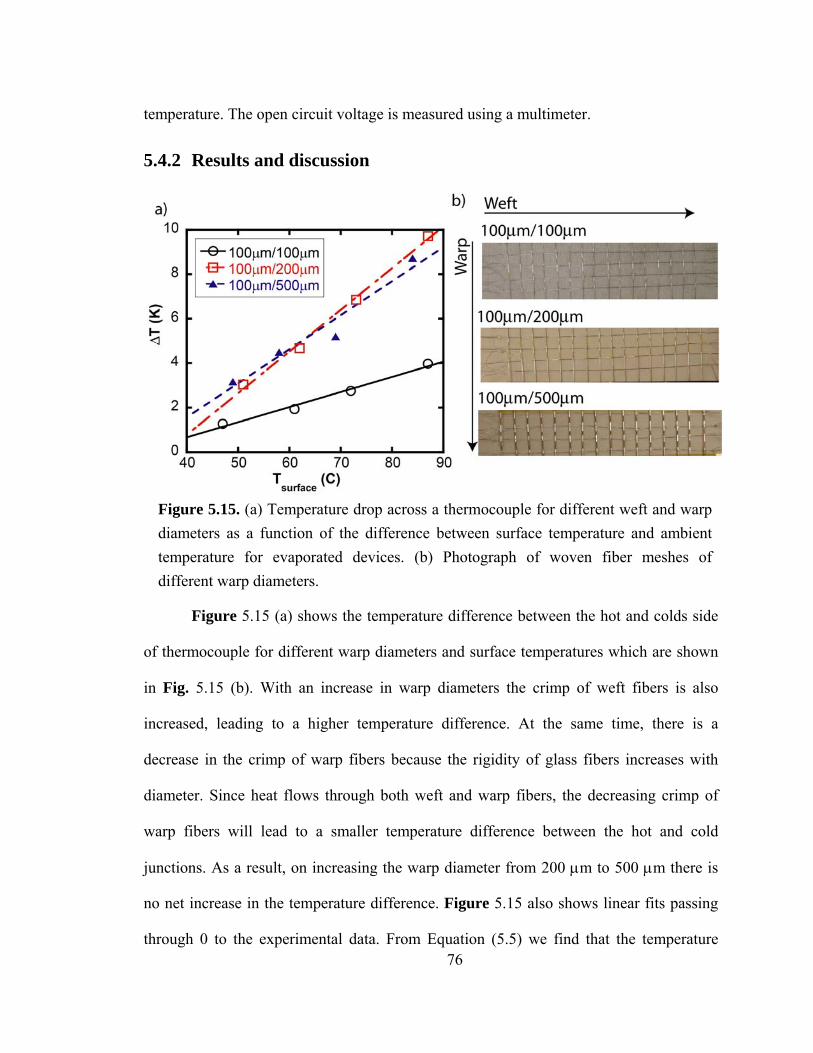
76
temperature. The open circuit voltage is measured using a multimeter.
5.4.2 Results and discussion
Figure 5.15 (a) shows the temperature difference between the hot and colds side
of thermocouple for different warp diameters and surface temperatures which are shown
in Fig. 5.15 (b). With an increase in warp diameters the crimp of weft fibers is also
increased, leading to a higher temperature difference. At the same time, there is a
decrease in the crimp of warp fibers because the rigidity of glass fibers increases with
diameter. Since heat flows through both weft and warp fibers, the decreasing crimp of
warp fibers will lead to a smaller temperature difference between the hot and cold
junctions. As a result, on increasing the warp diameter from 200 μm to 500 μm there is
no net increase in the temperature difference. Figure 5.15 also shows linear fits passing
through 0 to the experimental data. From Equation (5.5) we find that the temperature
Figure 5.15. (a) Temperature drop across a thermocouple for different weft and warp diameters as a function of the difference between surface temperature and ambient temperature for evaporated devices. (b) Photograph of woven fiber meshes of different warp diameters.
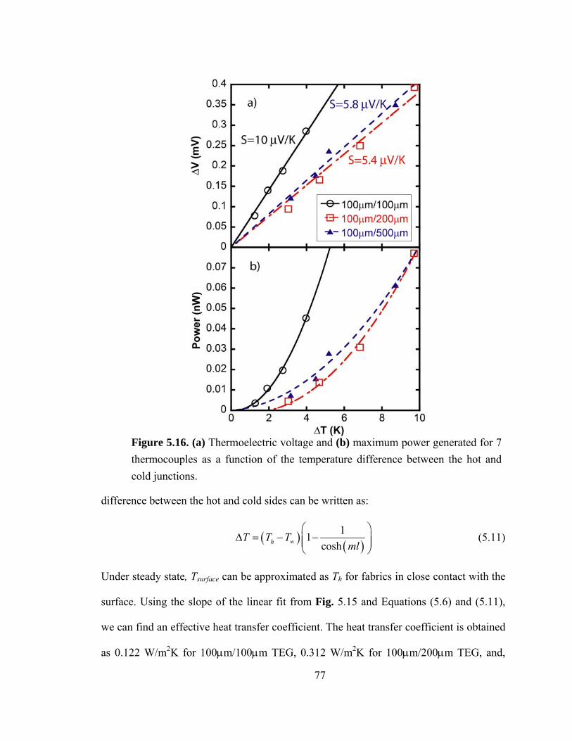
77
difference between the hot and cold sides can be written as:
( ) ( )11
coshhT T Tml∞
⎛ ⎞Δ = − −⎜ ⎟⎜ ⎟
⎝ ⎠ (5.11)
Under steady state, Tsurface can be approximated as Th for fabrics in close contact with the
surface. Using the slope of the linear fit from Fig. 5.15 and Equations (5.6) and (5.11),
we can find an effective heat transfer coefficient. The heat transfer coefficient is obtained
as 0.122 W/m2K for 100μm/100μm TEG, 0.312 W/m2K for 100μm/200μm TEG, and,
Figure 5.16. (a) Thermoelectric voltage and (b) maximum power generated for 7 thermocouples as a function of the temperature difference between the hot and cold junctions.
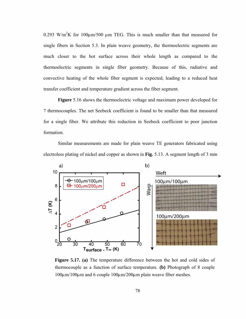
78
0.293 W/m2K for 100μm/500 μm TEG. This is much smaller than that measured for
single fibers in Section 5.3. In plain weave geometry, the thermoelectric segments are
much closer to the hot surface across their whole length as compared to the
thermoelectric segments in single fiber geometry. Because of this, radiative and
convective heating of the whole fiber segment is expected, leading to a reduced heat
transfer coefficient and temperature gradient across the fiber segment.
Figure 5.16 shows the thermoelectric voltage and maximum power developed for
7 thermocouples. The net Seebeck coefficient is found to be smaller than that measured
for a single fiber. We attribute this reduction in Seebeck coefficient to poor junction
formation.
Similar measurements are made for plain weave TE generators fabricated using
electroless plating of nickel and copper as shown in Fig. 5.13. A segment length of 3 mm
Figure 5.17. (a) The temperature difference between the hot and cold sides of thermocouple as a function of surface temperature. (b) Photograph of 8 couple 100μm/100μm and 6 couple 100μm/200μm plain weave fiber meshes.
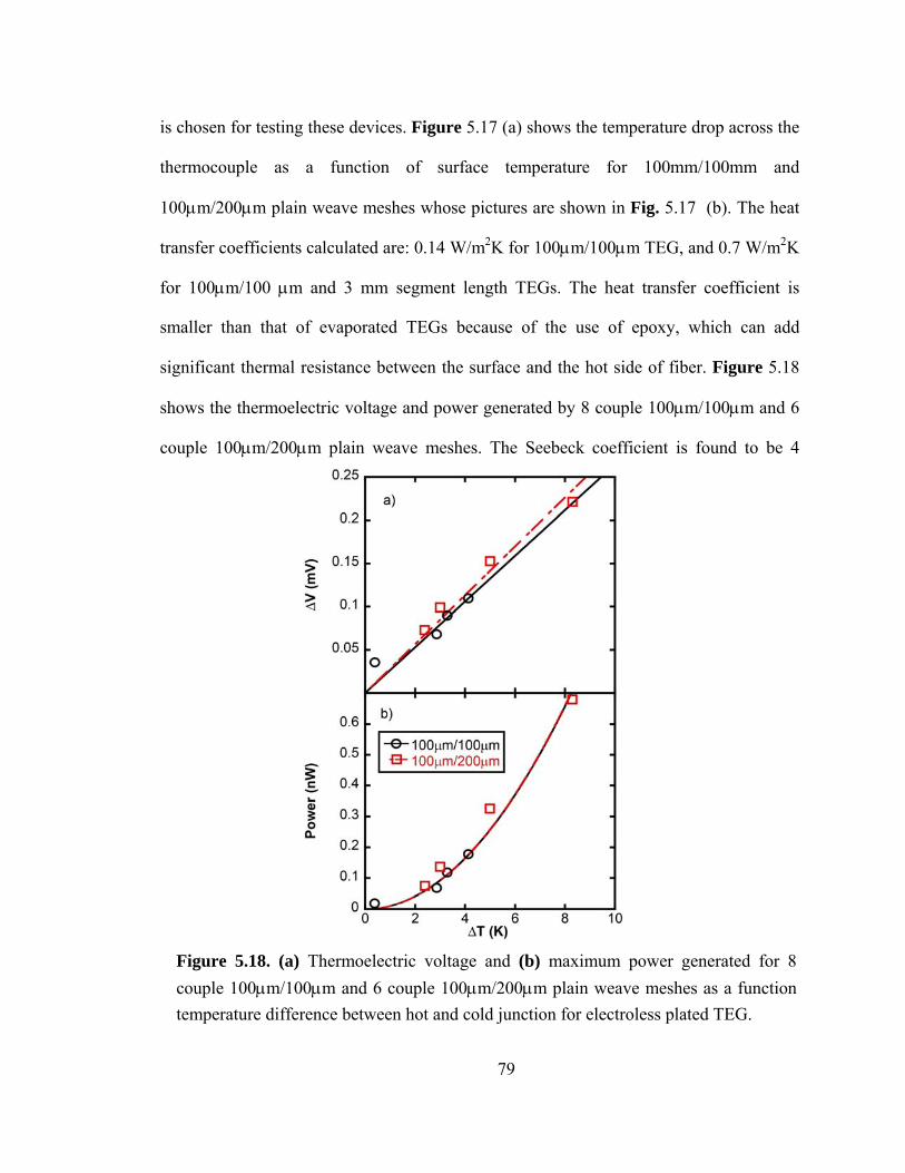
79
is chosen for testing these devices. Figure 5.17 (a) shows the temperature drop across the
thermocouple as a function of surface temperature for 100mm/100mm and
100μm/200μm plain weave meshes whose pictures are shown in Fig. 5.17 (b). The heat
transfer coefficients calculated are: 0.14 W/m2K for 100μm/100μm TEG, and 0.7 W/m2K
for 100μm/100 μm and 3 mm segment length TEGs. The heat transfer coefficient is
smaller than that of evaporated TEGs because of the use of epoxy, which can add
significant thermal resistance between the surface and the hot side of fiber. Figure 5.18
shows the thermoelectric voltage and power generated by 8 couple 100μm/100μm and 6
couple 100μm/200μm plain weave meshes. The Seebeck coefficient is found to be 4
Figure 5.18. (a) Thermoelectric voltage and (b) maximum power generated for 8 couple 100μm/100μm and 6 couple 100μm/200μm plain weave meshes as a function temperature difference between hot and cold junction for electroless plated TEG.
80
μV/K for 100μm/100μm plain weave meshes and 4 μV/K for 100μm/200μm plain weave
meshes. The lower Seebeck coefficient can arise because of poor junction quality or poor
quality of electroless plated films. The power generated is proportional to square of
thermoelectric voltage, and hence scales as the square of temperature difference. Using
electroless plating, a larger thickness of metal layers can be obtained, yielding a smaller
electrical resistance. Hence, the maximum power produced is much higher than that
achievable in evaporated TEGs.
5.5 Summary We demonstrated novel fiber-shaped thermoelectric devices composed of thermally
evaporated or electroless plated thin film thermocouples for both single fiber and multiple
fiber plain weave devices. Single fiber thermoelectric power generators were
characterized by measuring open circuit voltage and electrical power output as a function
of the temperature difference between the junctions. The measurements were extended to
different thermocouple segment lengths, different material systems, and different fiber
geometries by applying simple heat transfer analysis based on the measured data. These
theoretical and experimental analyses show that fiber-based thermoelectric devices can be
utilized to make flexible thermoelectric power generators for waste heat recovery. In
particular, thicker semiconductor films evaporated on hollow, low thermal conductivity
polymer substrates offer a good opportunity to extract and convert a relatively large
amount of heat energy from arbitrarily shaped heat sources.
Multiple fiber thermoelectric power generators were demonstrated using plain weave
textile geometries. Polyimide fibers of diameter 100μm were woven with polyimide
fibers of diameter in range 100μm-500μm. Thin film metal thermocouples were
81
fabricated using either thermal evaporation of Ni-Ag thermocouples or a combination of
thermal evaporation and electroless plating of Ni-Cu thermocouples. Although, the
convective cooling for plain weave geometries is adversely affected because of close
spacing to hot surface, this technique can lead to fabrication of a large number of
thermocouples per unit area. For example, with close packing of 100μm fibers and a
segment length of 1mm, upto 500 thermocouples can be fabricated per cm2. In
comparison, commercially available thermoelectric power generators have about 10
thermocouples per cm2. A high thermocouple density is expected to offset the low
efficiency expected from thin film thermoelectric devices. Other weave geometries such
as twill, matt, and satin require more complicated weaving techniques but are possible
candidates for textile based thermoelectric power generators.
82
Chapter 6
Organic photovoltaics The photovoltaic effect consists of the conversion of light into electricity.
Photovoltaic devices are based on the photoelectric effect, which holds that a minimum
amount of energy given by the work function of a material is needed to absorb a photon
and eject an electron from the material [9]. Semiconductor solar cells are based on the
internal photoelectric effect in which an electron moves from the valence band to the
conduction band upon absorption of a photon.
Most photovoltaic devices are made from inorganic semiconductors such as silicon
(amorphous and crystalline), II-VI compounds (CdTe or CdS) and chalcogenides
(CuInSe2 or CuInGaSe2) [86]. These materials consist of covalently bonded atoms which
support strong delocalization of electronic wavefunctions and the formation of bands.
Organic semiconductors, on the other hand, consist of Van der Waals bonded molecules
made up of conjugate bonded carbon and hydrogen atoms. The presence of conjugate
bonds results in a large delocalization of electronic wavefunctions over single molecules.
However, Van der Waals interactions are very weak, causing most organic crystals to
retain the electronic properties of single molecules. In addition, these weak
intermolecular forces result in significant differences in charge transport. While charge
transport in inorganic semiconductors occurs through band transport, in organic
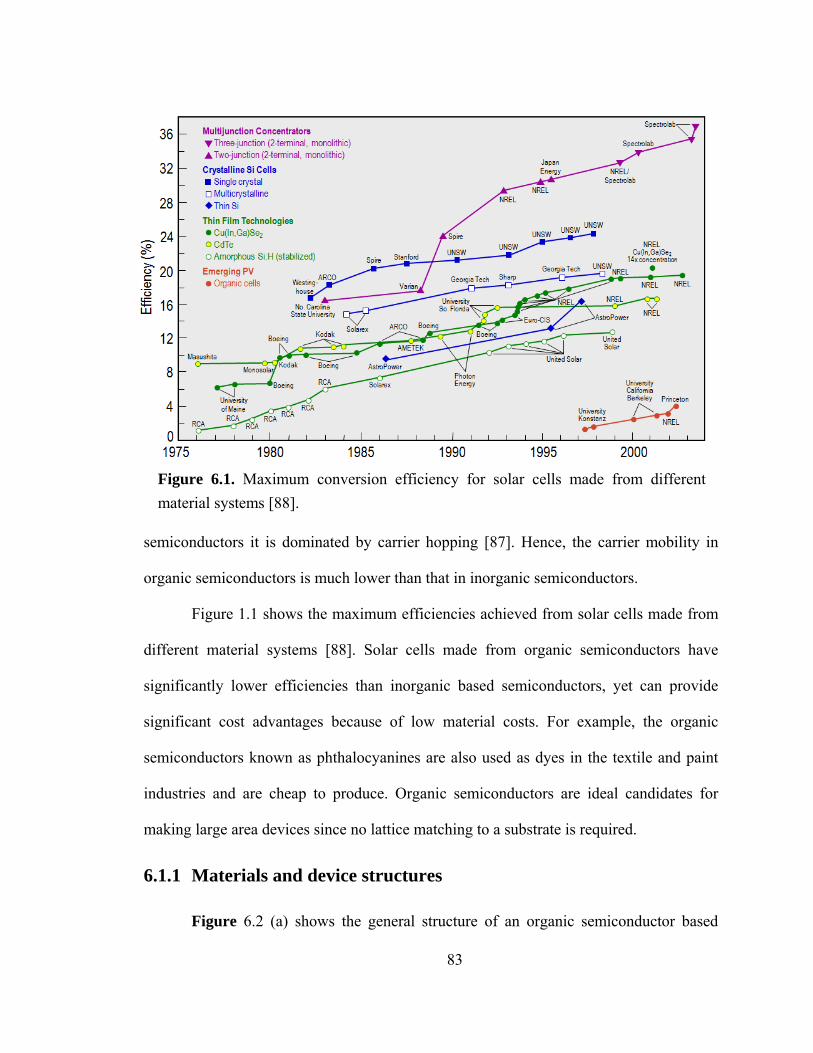
83
semiconductors it is dominated by carrier hopping [87]. Hence, the carrier mobility in
organic semiconductors is much lower than that in inorganic semiconductors.
Figure 1.1 shows the maximum efficiencies achieved from solar cells made from
different material systems [88]. Solar cells made from organic semiconductors have
significantly lower efficiencies than inorganic based semiconductors, yet can provide
significant cost advantages because of low material costs. For example, the organic
semiconductors known as phthalocyanines are also used as dyes in the textile and paint
industries and are cheap to produce. Organic semiconductors are ideal candidates for
making large area devices since no lattice matching to a substrate is required.
6.1.1 Materials and device structures
Figure 6.2 (a) shows the general structure of an organic semiconductor based
Figure 6.1. Maximum conversion efficiency for solar cells made from different material systems [88].
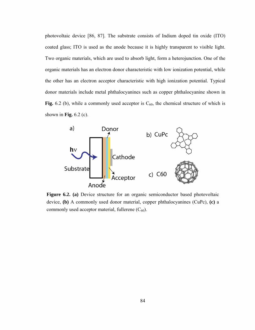
84
photovoltaic device [86, 87]. The substrate consists of Indium doped tin oxide (ITO)
coated glass; ITO is used as the anode because it is highly transparent to visible light.
Two organic materials, which are used to absorb light, form a heterojunction. One of the
organic materials has an electron donor characteristic with low ionization potential, while
the other has an electron acceptor characteristic with high ionization potential. Typical
donor materials include metal phthalocyanines such as copper phthalocyanine shown in
Fig. 6.2 (b), while a commonly used acceptor is C60, the chemical structure of which is
shown in Fig. 6.2 (c).
Figure 6.2. (a) Device structure for an organic semiconductor based photovoltaic device, (b) A commonly used donor material, copper phthalocyanines (CuPc), (c) a commonly used acceptor material, fullerene (C60).
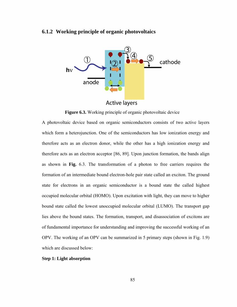
85
6.1.2 Working principle of organic photovoltaics
A photovoltaic device based on organic semiconductors consists of two active layers
which form a heterojunction. One of the semiconductors has low ionization energy and
therefore acts as an electron donor, while the other has a high ionization energy and
therefore acts as an electron acceptor [86, 89]. Upon junction formation, the bands align
as shown in Fig. 6.3. The transformation of a photon to free carriers requires the
formation of an intermediate bound electron-hole pair state called an exciton. The ground
state for electrons in an organic semiconductor is a bound state the called highest
occupied molecular orbital (HOMO). Upon excitation with light, they can move to higher
bound state called the lowest unoccupied molecular orbital (LUMO). The transport gap
lies above the bound states. The formation, transport, and disassociation of excitons are
of fundamental importance for understanding and improving the successful working of an
OPV. The working of an OPV can be summarized in 5 primary steps (shown in Fig. 1.9)
which are discussed below:
Step 1: Light absorption
Figure 6.3. Working principle of organic photovoltaic device

86
Light absorption in organic semiconductors occurs through the formation of bound
electron-hole pairs called excitons as shown in Fig. 6.4. This is in contrast to inorganic
semiconductors where light absorption results in the formation of free carriers. This
distinction in formation of excitons or free carriers arises due very different dielectric
constants in organic and inorganic semiconductors. Organic semiconductors have very
low dielectric constants (typically in the range of 3-4) while the dielectric constant of
inorganic semiconductors is 2-3 times higher. As a result, the binding energy of excitons,
which is inversely proportional to square of the dielectric constant, is few hundreds of
meV in organic semiconductors. In comparison, the binding energies of excitons are only
few meV in inorganic semiconductors, which is comparable to the thermal energy (kBT =
26 meV at room temperature). Hence, the formation of excitons in inorganic
Figure 6.4. Excitation of electrons upon absorption of a photon leads to formation of bound states called excitons. S0 is the ground state, S1 is first singlet excited state also called a Frenkel exciton, S2 is the second singlet excited state, and T1 and T2 are the first and second excited triplet states.
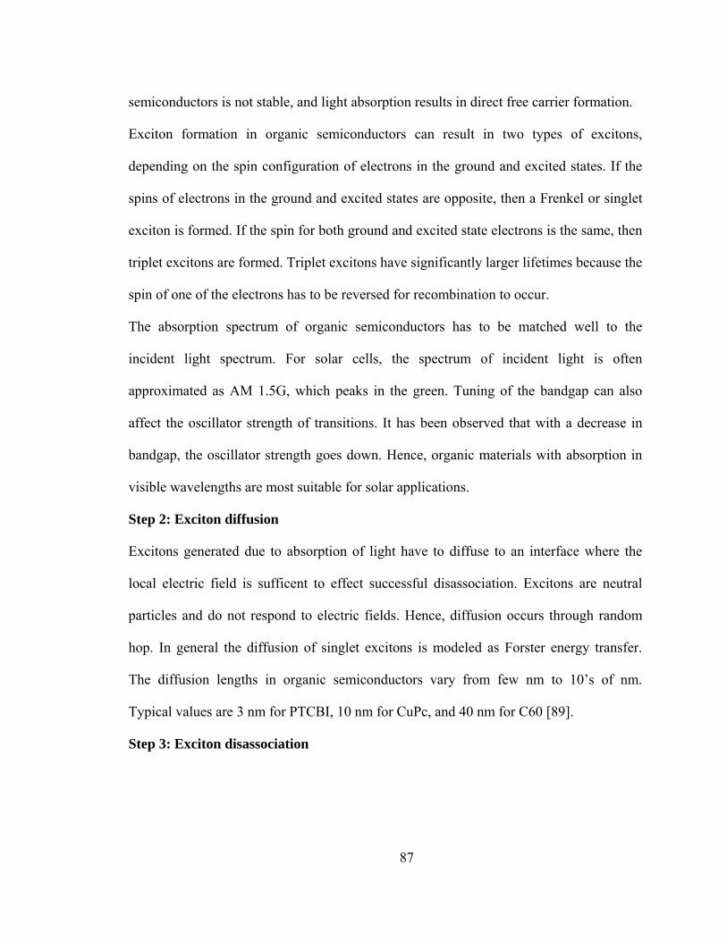
87
semiconductors is not stable, and light absorption results in direct free carrier formation.
Exciton formation in organic semiconductors can result in two types of excitons,
depending on the spin configuration of electrons in the ground and excited states. If the
spins of electrons in the ground and excited states are opposite, then a Frenkel or singlet
exciton is formed. If the spin for both ground and excited state electrons is the same, then
triplet excitons are formed. Triplet excitons have significantly larger lifetimes because the
spin of one of the electrons has to be reversed for recombination to occur.
The absorption spectrum of organic semiconductors has to be matched well to the
incident light spectrum. For solar cells, the spectrum of incident light is often
approximated as AM 1.5G, which peaks in the green. Tuning of the bandgap can also
affect the oscillator strength of transitions. It has been observed that with a decrease in
bandgap, the oscillator strength goes down. Hence, organic materials with absorption in
visible wavelengths are most suitable for solar applications.
Step 2: Exciton diffusion
Excitons generated due to absorption of light have to diffuse to an interface where the
local electric field is sufficent to effect successful disassociation. Excitons are neutral
particles and do not respond to electric fields. Hence, diffusion occurs through random
hop. In general the diffusion of singlet excitons is modeled as Forster energy transfer.
The diffusion lengths in organic semiconductors vary from few nm to 10’s of nm.
Typical values are 3 nm for PTCBI, 10 nm for CuPc, and 40 nm for C60 [89].
Step 3: Exciton disassociation
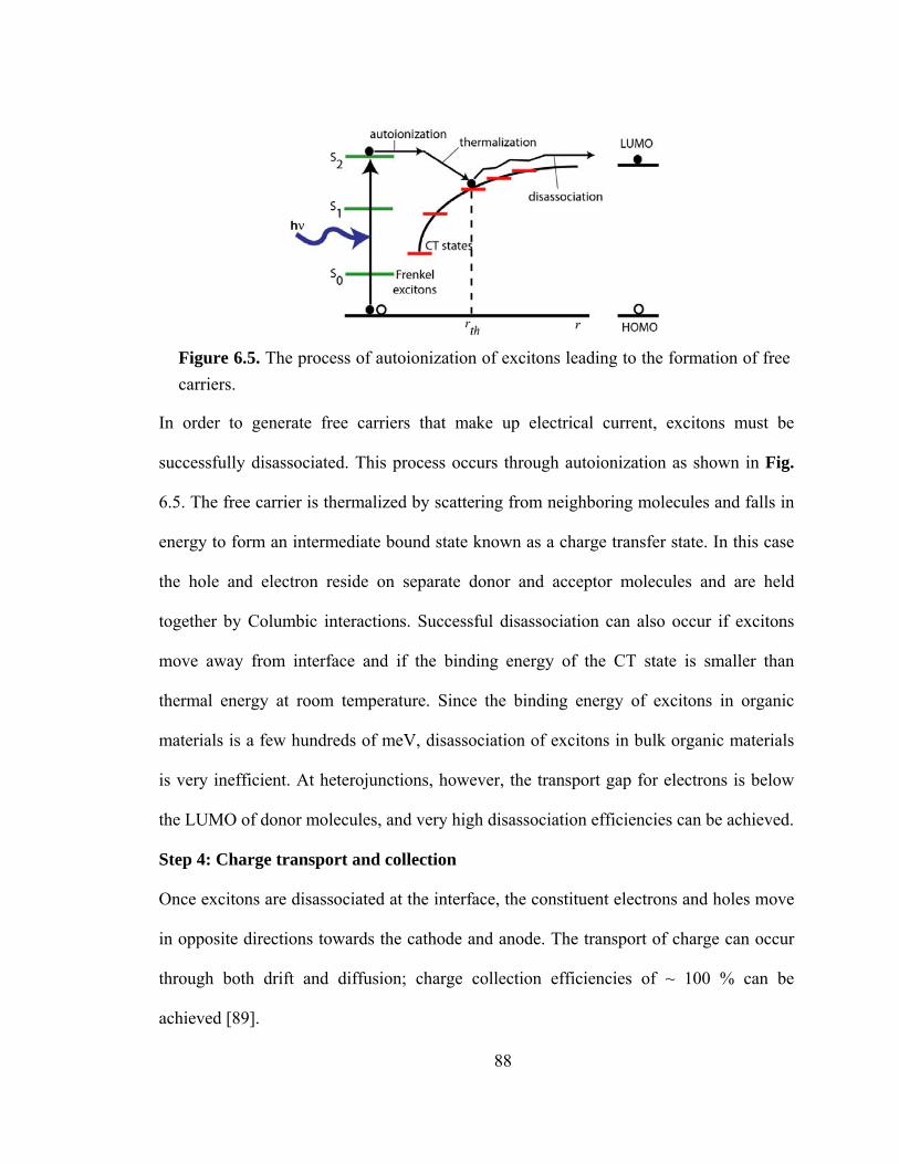
88
In order to generate free carriers that make up electrical current, excitons must be
successfully disassociated. This process occurs through autoionization as shown in Fig.
6.5. The free carrier is thermalized by scattering from neighboring molecules and falls in
energy to form an intermediate bound state known as a charge transfer state. In this case
the hole and electron reside on separate donor and acceptor molecules and are held
together by Columbic interactions. Successful disassociation can also occur if excitons
move away from interface and if the binding energy of the CT state is smaller than
thermal energy at room temperature. Since the binding energy of excitons in organic
materials is a few hundreds of meV, disassociation of excitons in bulk organic materials
is very inefficient. At heterojunctions, however, the transport gap for electrons is below
the LUMO of donor molecules, and very high disassociation efficiencies can be achieved.
Step 4: Charge transport and collection
Once excitons are disassociated at the interface, the constituent electrons and holes move
in opposite directions towards the cathode and anode. The transport of charge can occur
through both drift and diffusion; charge collection efficiencies of ~ 100 % can be
achieved [89].
Figure 6.5. The process of autoionization of excitons leading to the formation of free carriers.
89
6.2 Summary In this chapter, the basic photophysics of organic semiconductors was discussed. The
process from light absorption to free carrier generation can be divided into five main
steps. The efficiency of organic photovoltaic devices is mainly determined by the tradeoff
between exciton diffusion length and absorption length, which are dependent on the
nature of exciton. The open circuit voltage is determined by the disassociation of excitons
at heterojunctions. Charge transfer excitons play an important role in this process and
their identification at heterojunctions is important. The morphology and crystal structure
can affect the intermolecular interactions significantly leading to change in excitonic
properties. In chapter 7, we use modulation spectroscopy based on temperature to
determine excitonic nature in CuPc thin films. The effect of different crystal structure on
the optical spectrum and excitonic properties is also studied. Finally, assuming the dipole
moment matrix element for charge transfer excitons to decay exponentially, we determine
the coefficient of exponential decay.
90
Chapter 7
Temperature Modulation Spectroscopy for
Studying Excitonic Properties of Organic
Semiconductors
7.1 Introduction Organic thin films are finding applications in next-generation light-emitting and
photovoltaic devices [89, 90]. The correlation of molecular structure and optical
properties is a fundamental problem in condensed matter physics and is central to the
design of optoelectronic materials and devices. While strong carrier localization in
organic semiconductors is known to lead to the generation of bound electron-hole pairs
(excitons) during light absorption or emission, the complex physical structure of most
organic materials has precluded a detailed understanding of the processes governing
exciton formation and transport. However, this carrier localization entails a sensitivity of
exciton formation to perturbations in physical structure that can be significantly stronger
than that of optical processes involving delocalized free carriers in inorganic crystalline
semiconductors. Here we demonstrate that perturbation by thermal expansion offers a
powerful and convenient method to characterize the excitonic properties of organic
semiconductors.
The light absorption or emission spectrum of an organic material is determined by the
91
superimposed contributions of a number of excitonic transitions, each of which is
typically described in terms of transition energy, oscillator strength, and lifetime
broadening. The oscillator strength describes the interaction strength between the two
states involved in the transition, while the lifetime broadening determines the exciton
coherence length, affecting exciton transport properties such as diffusion length [87].
Exciton formation or recombination typically occurs through the direct transfer of charge
between highest occupied molecular orbital (HOMO) and lowest unoccupied molecular
orbital (LUMO) states. For charge transfer (CT) excitons, the transition occurs between
HOMO and LUMO levels that are on neighboring molecules, while for Frenkel excitons
it occurs between levels on the same molecule [91, 92]. Frenkel and CT excitons have
significant differences in diffusion length, dissociation efficiency, and other transport
properties [93, 94].
The intermolecular electronic transfer integral plays a key role in quantifying charge
transfer in molecular crystals [95]. Photoemission spectroscopy has been used to derive
transfer integrals for intraband (HOMO-HOMO and LUMO-LUMO) intermolecular
transitions [96], which govern carrier mobility. However, no measurements have been
made of interband (HOMO-LUMO) intermolecular transfer integrals, which govern the
formation and dissociation of CT excitons. Here we demonstrate the use of thermal
modulation to obtain interband transfer integrals; a simple variation of the technique in
which modulated electrical current rather than optical transmission was measured could
similarly be applied to obtain intraband integrals.
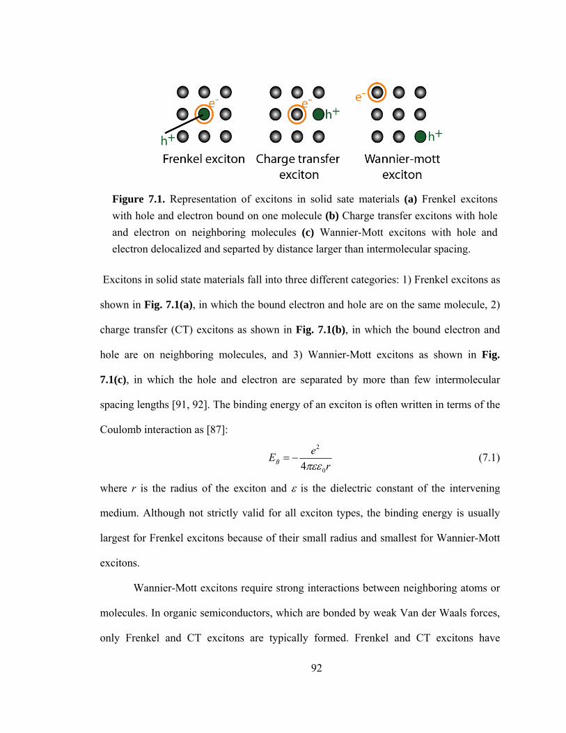
92
Excitons in solid state materials fall into three different categories: 1) Frenkel excitons as
shown in Fig. 7.1(a), in which the bound electron and hole are on the same molecule, 2)
charge transfer (CT) excitons as shown in Fig. 7.1(b), in which the bound electron and
hole are on neighboring molecules, and 3) Wannier-Mott excitons as shown in Fig.
7.1(c), in which the hole and electron are separated by more than few intermolecular
spacing lengths [91, 92]. The binding energy of an exciton is often written in terms of the
Coulomb interaction as [87]:
2
04BeE
rπεε= − (7.1)
where r is the radius of the exciton and ε is the dielectric constant of the intervening
medium. Although not strictly valid for all exciton types, the binding energy is usually
largest for Frenkel excitons because of their small radius and smallest for Wannier-Mott
excitons.
Wannier-Mott excitons require strong interactions between neighboring atoms or
molecules. In organic semiconductors, which are bonded by weak Van der Waals forces,
only Frenkel and CT excitons are typically formed. Frenkel and CT excitons have
Figure 7.1. Representation of excitons in solid sate materials (a) Frenkel excitons with hole and electron bound on one molecule (b) Charge transfer excitons with hole and electron on neighboring molecules (c) Wannier-Mott excitons with hole and electron delocalized and separted by distance larger than intermolecular spacing.
93
significantly different transport properties [93, 94]. While Frenkel excitons have a larger
diffusion length than CT excitons, their smaller radius often leads to lower dissociation
efficiency. Furthermore, Frenkel and CT excitons may couple to each other; for example,
light absorption in an organic photovoltaic cell may initially create a Frenkel exciton,
which diffuses to the donor-acceptor interface and forms a CT exciton, which then
dissociates to generate photocurrent [87, 91]. To obtain high quantum efficiency in
photovoltaic devices, both large diffusion length and high exciton dissociation efficiency
are desired. In the context of organic light-emitting devices, electroluminescence has
mainly been attributed to recombination on individual molecules that is limited by free
carrier diffusion (Langevin recombination). However, optical recombination can also
occur through the formation of a CT state [91] if the binding energy is large.
The formation or recombination of CT exciton states typically occurs through the direct
transfer of charge between the highest occupied molecular orbital (HOMO) of one
molecule and the lowest unoccupied molecular orbital (LUMO) of a neighboring
molecule. The strength of the CT state depends on the spatial overlap of HOMO and
LUMO electronic wavefunctions, which we refer to as interband electronic coupling.
Because of the spheroidal shapes of molecular wavefunctions, electronic coupling is
often written as an exponentially decaying function of intermolecular separation [97].
The decay coefficient quantifies the strength of electronic coupling and depends on the
size and shape of the electronic wavefunctions as well as the binding energy of the
electron on the donor site. For charge transfer states in liquid and glassy media, the decay
coefficient has been derived by varying the concentrations of donor and acceptor
molecules and measuring time-resolved optical spectra [97, 98]. As we show below,
thermal expansion provides a convenient means to measure this important parameter in
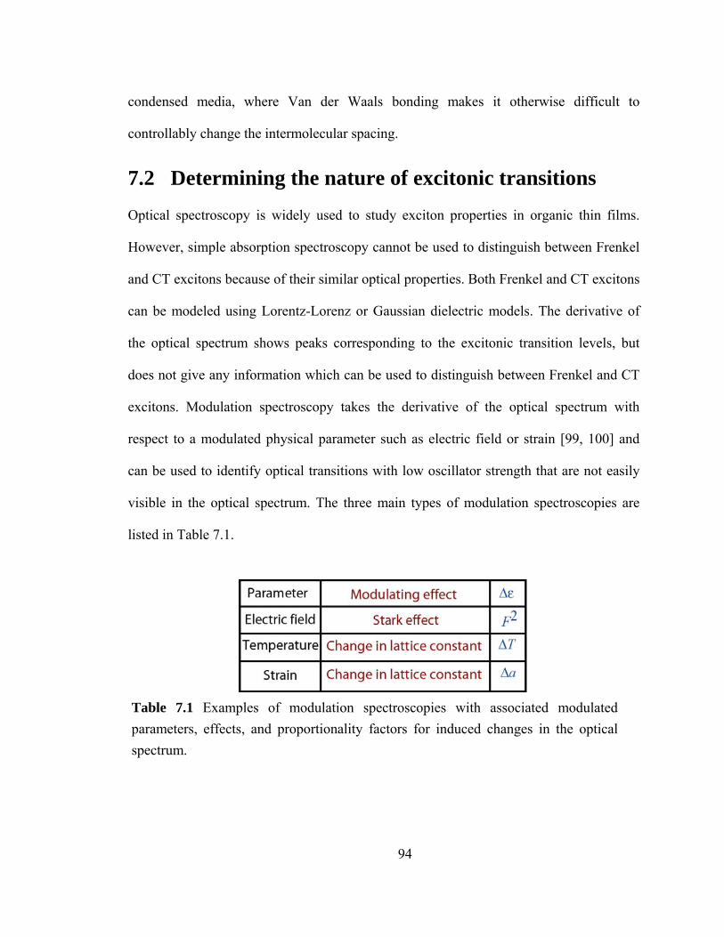
94
condensed media, where Van der Waals bonding makes it otherwise difficult to
controllably change the intermolecular spacing.
7.2 Determining the nature of excitonic transitions Optical spectroscopy is widely used to study exciton properties in organic thin films.
However, simple absorption spectroscopy cannot be used to distinguish between Frenkel
and CT excitons because of their similar optical properties. Both Frenkel and CT excitons
can be modeled using Lorentz-Lorenz or Gaussian dielectric models. The derivative of
the optical spectrum shows peaks corresponding to the excitonic transition levels, but
does not give any information which can be used to distinguish between Frenkel and CT
excitons. Modulation spectroscopy takes the derivative of the optical spectrum with
respect to a modulated physical parameter such as electric field or strain [99, 100] and
can be used to identify optical transitions with low oscillator strength that are not easily
visible in the optical spectrum. The three main types of modulation spectroscopies are
listed in Table 7.1.
Table 7.1 Examples of modulation spectroscopies with associated modulated parameters, effects, and proportionality factors for induced changes in the optical spectrum.
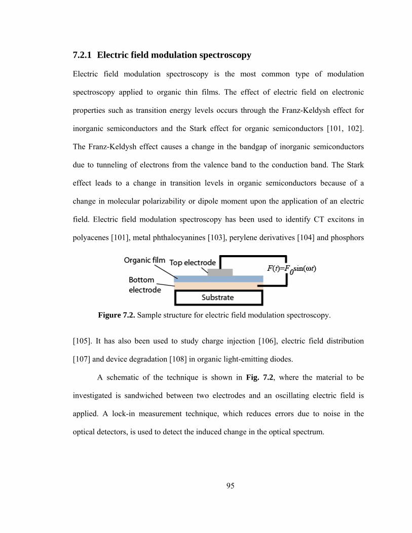
95
7.2.1 Electric field modulation spectroscopy
Electric field modulation spectroscopy is the most common type of modulation
spectroscopy applied to organic thin films. The effect of electric field on electronic
properties such as transition energy levels occurs through the Franz-Keldysh effect for
inorganic semiconductors and the Stark effect for organic semiconductors [101, 102].
The Franz-Keldysh effect causes a change in the bandgap of inorganic semiconductors
due to tunneling of electrons from the valence band to the conduction band. The Stark
effect leads to a change in transition levels in organic semiconductors because of a
change in molecular polarizability or dipole moment upon the application of an electric
field. Electric field modulation spectroscopy has been used to identify CT excitons in
polyacenes [101], metal phthalocyanines [103], perylene derivatives [104] and phosphors
[105]. It has also been used to study charge injection [106], electric field distribution
[107] and device degradation [108] in organic light-emitting diodes.
A schematic of the technique is shown in Fig. 7.2, where the material to be
investigated is sandwiched between two electrodes and an oscillating electric field is
applied. A lock-in measurement technique, which reduces errors due to noise in the
optical detectors, is used to detect the induced change in the optical spectrum.
Figure 7.2. Sample structure for electric field modulation spectroscopy.
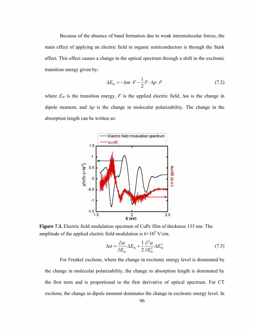
96
Because of the absence of band formation due to weak intermolecular forces, the
main effect of applying an electric field in organic semiconductors is through the Stark
effect. This effect causes a change in the optical spectrum through a shift in the excitonic
transition energy given by:
012iE m F F p FΔ = −Δ ⋅ − ⋅ Δ ⋅ (7.2)
where E0i is the transition energy, F is the applied electric field, Δm is the change in
dipole moment, and Δp is the change in molecular polarizability. The change in the
absorption length can be written as:
2
20 02
0 0
12i i
i i
E EE Eα αα ∂ ∂
Δ = Δ + Δ∂ ∂
(7.3)
For Frenkel excitons, where the change in excitonic energy level is dominated by
the change in molecular polarizability, the change in absorption length is dominated by
the first term and is proportional to the first derivative of optical spectrum. For CT
excitons, the change in dipole moment dominates the change in excitonic energy level. In
Figure 7.3. Electric field modulation spectrum of CuPc film of thickness 133 nm. The amplitude of the applied electric field modulation is 6×10⁵ V/cm.
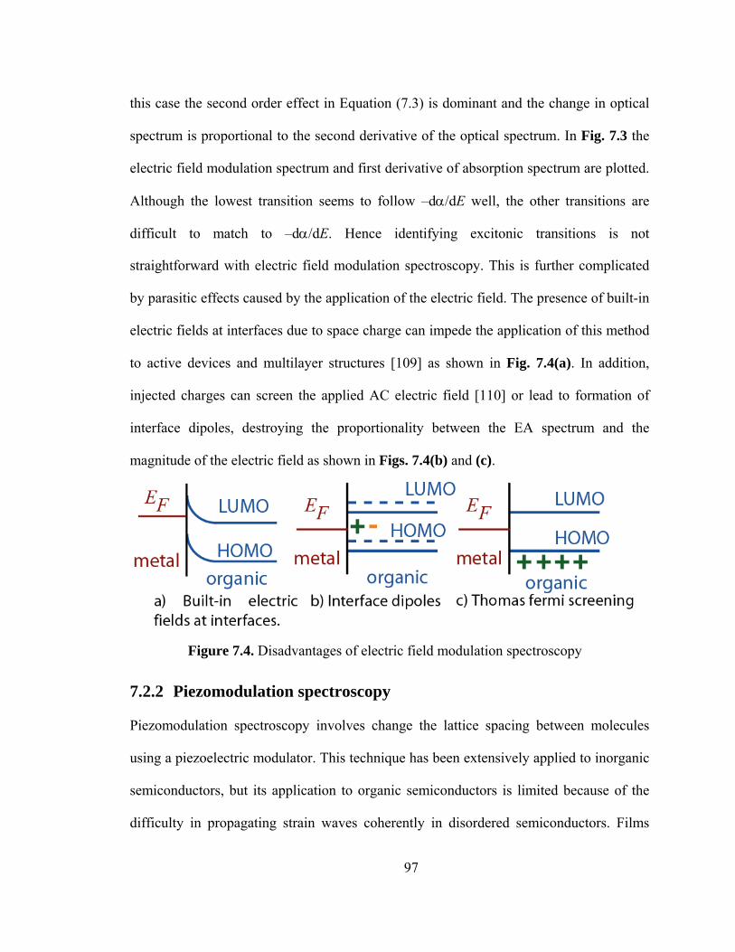
97
this case the second order effect in Equation (7.3) is dominant and the change in optical
spectrum is proportional to the second derivative of the optical spectrum. In Fig. 7.3 the
electric field modulation spectrum and first derivative of absorption spectrum are plotted.
Although the lowest transition seems to follow –dα/dE well, the other transitions are
difficult to match to –dα/dE. Hence identifying excitonic transitions is not
straightforward with electric field modulation spectroscopy. This is further complicated
by parasitic effects caused by the application of the electric field. The presence of built-in
electric fields at interfaces due to space charge can impede the application of this method
to active devices and multilayer structures [109] as shown in Fig. 7.4(a). In addition,
injected charges can screen the applied AC electric field [110] or lead to formation of
interface dipoles, destroying the proportionality between the EA spectrum and the
magnitude of the electric field as shown in Figs. 7.4(b) and (c).
7.2.2 Piezomodulation spectroscopy
Piezomodulation spectroscopy involves change the lattice spacing between molecules
using a piezoelectric modulator. This technique has been extensively applied to inorganic
semiconductors, but its application to organic semiconductors is limited because of the
difficulty in propagating strain waves coherently in disordered semiconductors. Films
Figure 7.4. Disadvantages of electric field modulation spectroscopy
98
have to be made with long distance order using a method such as Langmuir-Blodgett.
Low temperature measurements are also needed to successfully propagate strain.
7.3 Temperature modulation spectroscopy
7.3.1 Theory
The effect of temperature on the dielectric constant occurs through both thermal
expansion and increased phonon occupation. The average induced molecular
polarizability for ith optical transition can be written as [111]:
( )2
0 ,2 20
2 i DA ii
i i
E VE
E E iQ Eα =
− −h (7.4)
where VDA,i is the dipole moment matrix element of ith transition, E0i is the transition
energy, Qi is the lifetime broadening, E is the energy of incident light. We make the
assumption that the polarizability tensor has only one component in a local coordinate
space (x,y,z) given by αxx,i= α i. The polarizability due to the electric field component
along the X direction in laboratory coordinates (X,Y,Z) is then given by:
( )2, , cosXX i xx i iXxα α= (7.5)
with all other components of the polarizability tensor being 0. Xxi is the angle between
the laboratory X-axis and the local x-axis for transition i. The net polarizability can be
written by summing contributions from all electronic transitions:
( ) ( )2 20 ,
2 20
cos2 i DA i i
i i i
E V XxE
E E iQ Eα =
− −∑h (7.6)
and the dielectric constant can be written as:
99
( ) ( ) ( )2 20 ,
2 20
cos4 8 i DA i i
i i i
E V XxE N E N
E E iQ Eε ε π α ε π∞ ∞= + = +
− −∑h (7.7)
where N is the number density of molecules. Phenomenologically we can write the
dielectric constant as:
( )2
2 20
pi
i i i
EE
E E iQ Eε ε∞= +
− −∑ (7.8)
where Epi is the effective oscillator strength. From Equations (7.7) and (7.8), the effective
oscillator strength can be written as:
( )2 2 20 ,8 cospi i DA i iE NE V Xxπ= h (7.9)
The change in oscillator strength with respect to temperature can be written as:
( )2
,02
0 ,
2 1 1 1 2 tanpi DA ii ii
pi i DA i
dE dVdE dXxdN XxE dT N dT E dT V dT dT
= + + − (7.10)
The first term on right hand side arises because of a change in the number density due to
Figure 7.5. The working principle of phase sensitive detection.
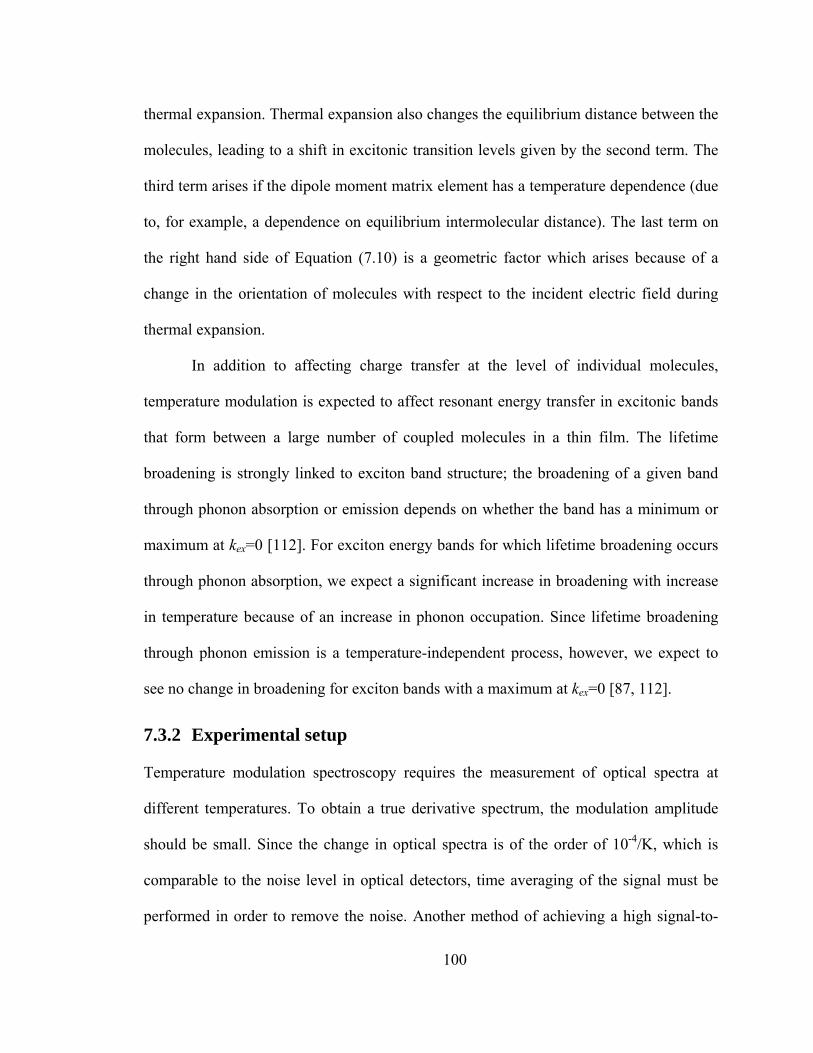
100
thermal expansion. Thermal expansion also changes the equilibrium distance between the
molecules, leading to a shift in excitonic transition levels given by the second term. The
third term arises if the dipole moment matrix element has a temperature dependence (due
to, for example, a dependence on equilibrium intermolecular distance). The last term on
the right hand side of Equation (7.10) is a geometric factor which arises because of a
change in the orientation of molecules with respect to the incident electric field during
thermal expansion.
In addition to affecting charge transfer at the level of individual molecules,
temperature modulation is expected to affect resonant energy transfer in excitonic bands
that form between a large number of coupled molecules in a thin film. The lifetime
broadening is strongly linked to exciton band structure; the broadening of a given band
through phonon absorption or emission depends on whether the band has a minimum or
maximum at kex=0 [112]. For exciton energy bands for which lifetime broadening occurs
through phonon absorption, we expect a significant increase in broadening with increase
in temperature because of an increase in phonon occupation. Since lifetime broadening
through phonon emission is a temperature-independent process, however, we expect to
see no change in broadening for exciton bands with a maximum at kex=0 [87, 112].
7.3.2 Experimental setup
Temperature modulation spectroscopy requires the measurement of optical spectra at
different temperatures. To obtain a true derivative spectrum, the modulation amplitude
should be small. Since the change in optical spectra is of the order of 10-4/K, which is
comparable to the noise level in optical detectors, time averaging of the signal must be
performed in order to remove the noise. Another method of achieving a high signal-to-
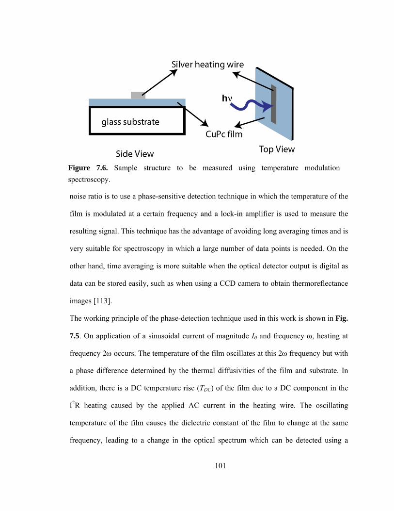
101
noise ratio is to use a phase-sensitive detection technique in which the temperature of the
film is modulated at a certain frequency and a lock-in amplifier is used to measure the
resulting signal. This technique has the advantage of avoiding long averaging times and is
very suitable for spectroscopy in which a large number of data points is needed. On the
other hand, time averaging is more suitable when the optical detector output is digital as
data can be stored easily, such as when using a CCD camera to obtain thermoreflectance
images [113].
The working principle of the phase-detection technique used in this work is shown in Fig.
7.5. On application of a sinusoidal current of magnitude I0 and frequency ω, heating at
frequency 2ω occurs. The temperature of the film oscillates at this 2ω frequency but with
a phase difference determined by the thermal diffusivities of the film and substrate. In
addition, there is a DC temperature rise (TDC) of the film due to a DC component in the
I2R heating caused by the applied AC current in the heating wire. The oscillating
temperature of the film causes the dielectric constant of the film to change at the same
frequency, leading to a change in the optical spectrum which can be detected using a
Figure 7.6. Sample structure to be measured using temperature modulation spectroscopy.
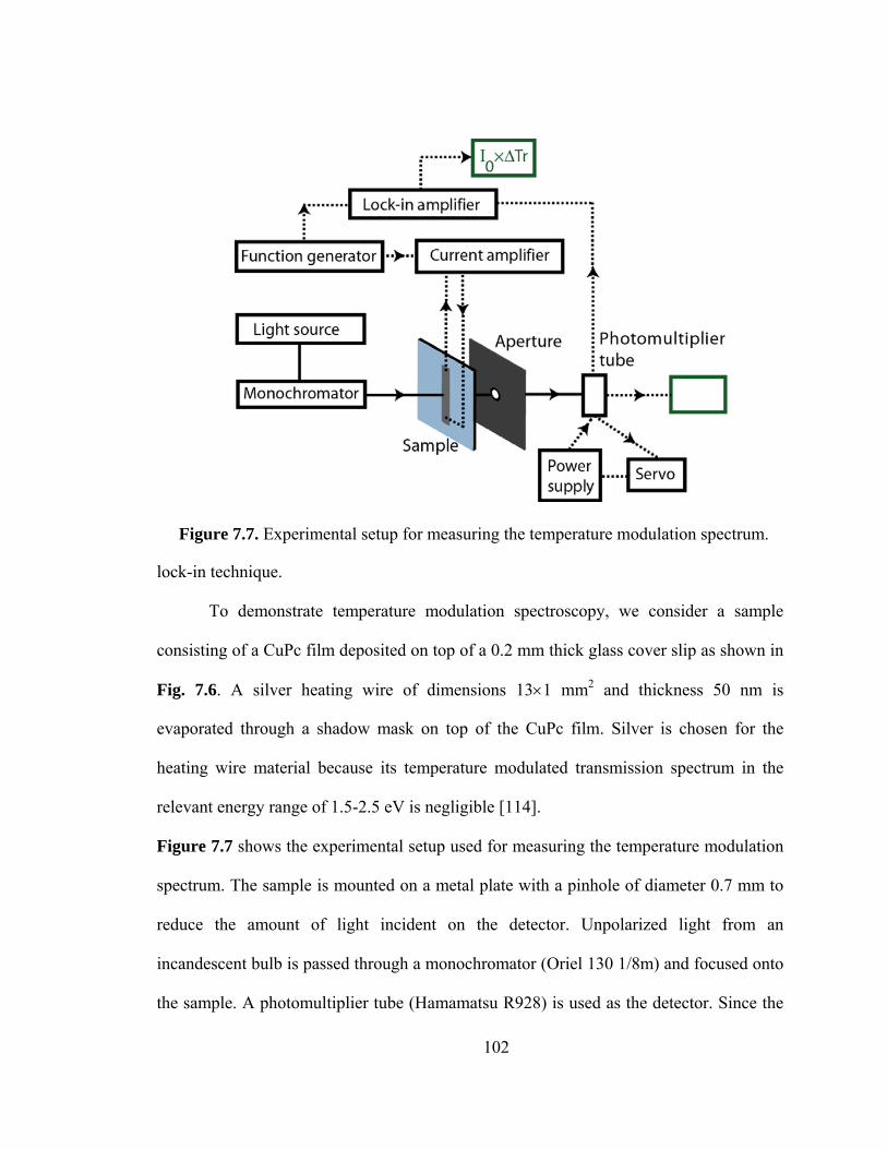
102
lock-in technique.
To demonstrate temperature modulation spectroscopy, we consider a sample
consisting of a CuPc film deposited on top of a 0.2 mm thick glass cover slip as shown in
Fig. 7.6. A silver heating wire of dimensions 13×1 mm2 and thickness 50 nm is
evaporated through a shadow mask on top of the CuPc film. Silver is chosen for the
heating wire material because its temperature modulated transmission spectrum in the
relevant energy range of 1.5-2.5 eV is negligible [114].
Figure 7.7 shows the experimental setup used for measuring the temperature modulation
spectrum. The sample is mounted on a metal plate with a pinhole of diameter 0.7 mm to
reduce the amount of light incident on the detector. Unpolarized light from an
incandescent bulb is passed through a monochromator (Oriel 130 1/8m) and focused onto
the sample. A photomultiplier tube (Hamamatsu R928) is used as the detector. Since the
Figure 7.7. Experimental setup for measuring the temperature modulation spectrum.
103
light intensity from an incandescent bulb varies with wavelength, the DC output of the
PMT also varies with the wavelength of light. To keep the DC output of PMT constant at
the maximum possible level, a computer based servo is used to change the gain of the
tube and achieve the desired constant DC output. For modulating the temperature of the
thin film, an AC current is passed through the heating wire. The AC current is generated
using a function generator to create a sine wave which is then input to a Howland current
pump [115]. Because the change in transmitted intensity (or the AC signal) is of the order
10-4, a lock-in amplifier (Stanford Research Systems 530) is used to sensitively measure
the AC signal from the PMT. To quantify the sign of the AC signal with change in
temperature, the temperature modulation spectrum of a thin gold film is measured and
compared with that in literature.[116] The magnitude of temperature modulation is
measured using a microthermocouple and is kept in the range of 1–1.5 K to satisfy the
small perturbation requirement needed in order to measure the derivative spectrum.
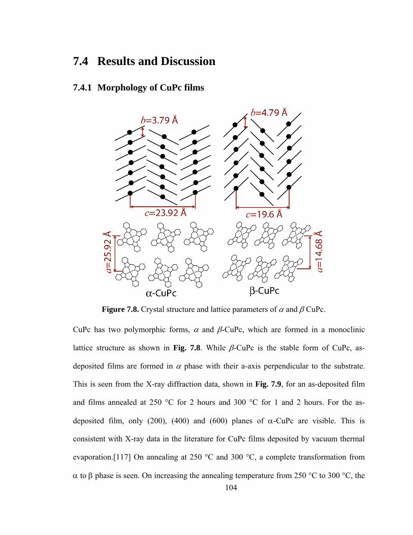
104
7.4 Results and Discussion
7.4.1 Morphology of CuPc films
CuPc has two polymorphic forms, α and β-CuPc, which are formed in a monoclinic
lattice structure as shown in Fig. 7.8. While β-CuPc is the stable form of CuPc, as-
deposited films are formed in α phase with their a-axis perpendicular to the substrate.
This is seen from the X-ray diffraction data, shown in Fig. 7.9, for an as-deposited film
and films annealed at 250 °C for 2 hours and 300 °C for 1 and 2 hours. For the as-
deposited film, only (200), (400) and (600) planes of α-CuPc are visible. This is
consistent with X-ray data in the literature for CuPc films deposited by vacuum thermal
evaporation.[117] On annealing at 250 °C and 300 °C, a complete transformation from
α to β phase is seen. On increasing the annealing temperature from 250 °C to 300 °C, the
Figure 7.8. Crystal structure and lattice parameters of α and β CuPc.
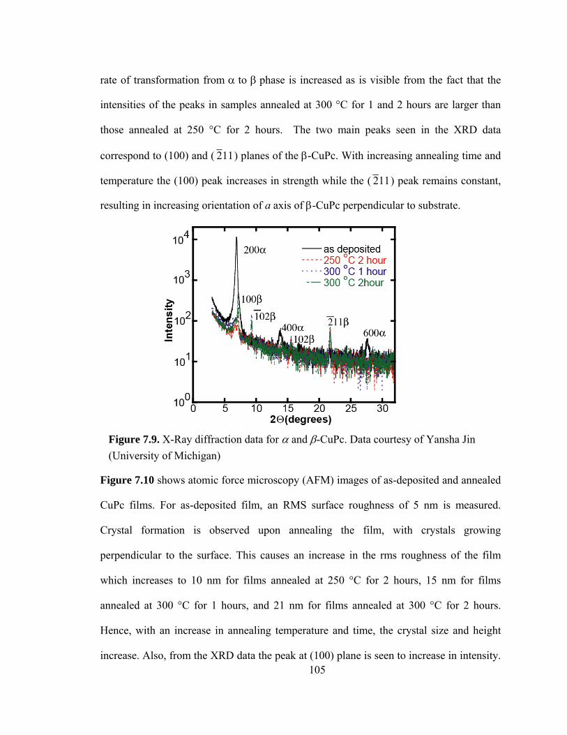
105
rate of transformation from α to β phase is increased as is visible from the fact that the
intensities of the peaks in samples annealed at 300 °C for 1 and 2 hours are larger than
those annealed at 250 °C for 2 hours. The two main peaks seen in the XRD data
correspond to (100) and ( 211) planes of the β-CuPc. With increasing annealing time and
temperature the (100) peak increases in strength while the ( 211) peak remains constant,
resulting in increasing orientation of a axis of β-CuPc perpendicular to substrate.
Figure 7.10 shows atomic force microscopy (AFM) images of as-deposited and annealed
CuPc films. For as-deposited film, an RMS surface roughness of 5 nm is measured.
Crystal formation is observed upon annealing the film, with crystals growing
perpendicular to the surface. This causes an increase in the rms roughness of the film
which increases to 10 nm for films annealed at 250 °C for 2 hours, 15 nm for films
annealed at 300 °C for 1 hours, and 21 nm for films annealed at 300 °C for 2 hours.
Hence, with an increase in annealing temperature and time, the crystal size and height
increase. Also, from the XRD data the peak at (100) plane is seen to increase in intensity.
Figure 7.9. X-Ray diffraction data for α and β-CuPc. Data courtesy of Yansha Jin (University of Michigan)
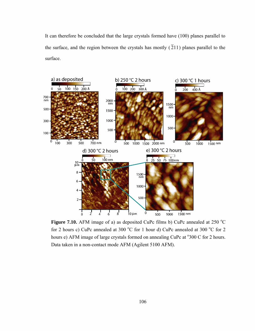
106
It can therefore be concluded that the large crystals formed have (100) planes parallel to
the surface, and the region between the crystals has mostly ( 211) planes parallel to the
surface.
Figure 7.10. AFM image of a) as deposited CuPc films b) CuPc annealed at 250 oC for 2 hours c) CuPc annealed at 300 oC for 1 hour d) CuPc annealed at 300 oC for 2 hours e) AFM image of large crystals formed on annealing CuPc at o300 C for 2 hours. Data taken in a non-contact mode AFM (Agilent 5100 AFM).
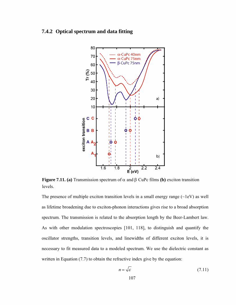
107
7.4.2 Optical spectrum and data fitting
The presence of multiple exciton transition levels in a small energy range (~1eV) as well
as lifetime broadening due to exciton-phonon interactions gives rise to a broad absorption
spectrum. The transmission is related to the absorption length by the Beer-Lambert law.
As with other modulation spectroscopies [101, 118], to distinguish and quantify the
oscillator strengths, transition levels, and linewidths of different exciton levels, it is
necessary to fit measured data to a modeled spectrum. We use the dielectric constant as
written in Equation (7.7) to obtain the refractive index give by the equation:
n ε= (7.11)
Figure 7.11. (a) Transmission spectrum of α and β CuPc films (b) exciton transition levels.
108
where n is refractive index. The transmission Tr(Ta) through the optically thin organic
film and optically thick substrate can be modeled using Fresnel coefficients, taking into
account multiple internal reflections using a matrix method [89] to obtain Epi (Ta), E0i
(Ta), and Qi (Ta) as fitting parameters. These parameters can then be determined for all
exciton transitions by minimizing the square of the error between the measured and
modeled transmission spectra.
A temperature modulation due to periodic heating, ΔTAC, causes a small change in the
dielectric constant of CuPc. The perturbed dielectric constant is given by:
( ) ( )( ) ( )
20
0 2 20 0 0
Pi ACAC
i i AC i AC
E T TT T
E T T E iQ T T Eε ε∞
+ Δ+ Δ = +
+ Δ − − + Δ∑ (7.12)
where T0 is the average temperature of the film. T0 is higher than Ta by ΔTDC, which is
due to steady state heating caused by the periodic heating. For small ΔTAC and ΔTDC
compared to Ta, the modulated values of Epi, E0i and Qi can be approximated by:
( ) ( ) ( )0pi
pi AC pi a DC AC
dEE T T E T T T
dT+ Δ = + Δ + Δ (7.13)
( ) ( ) ( )00 0 0 0
ii AC i DC AC
dEE T T E T T TdT
+ Δ = + Δ + Δ (7.14)
( ) ( ) ( )0 0i
i AC i DC ACdQQ T T Q T T TdT
+ Δ = + Δ + Δ (7.15)
The change in transmission ( ) ( )0 0ACTr Tr T T Tr TΔ = + Δ − can be modeled using Fresnel
coefficients and solving for interference effects in the multilayer system of optically thin
silver, optically thin CuPc, and optically thick substrate using a matrix method [89].
dEPi/dT, dE0i/dT, and dQi/dT can then be obtained by a least-square minimization of the
error in the modeled temperature modulation spectrum with respect to the measured
spectrum.
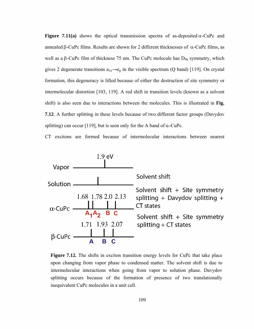
109
Figure 7.11(a) shows the optical transmission spectra of as-deposited α-CuPc and
annealed β-CuPc films. Results are shown for 2 different thicknesses of α-CuPc films, as
well as a β-CuPc film of thickness 75 nm. The CuPc molecule has D4h symmetry, which
gives 2 degenerate transitions a1u→eg in the visible spectrum (Q band) [119]. On crystal
formation, this degeneracy is lifted because of either the destruction of site symmetry or
intermolecular distortion [103, 119]. A red shift in transition levels (known as a solvent
shift) is also seen due to interactions between the molecules. This is illustrated in Fig.
7.12. A further splitting in these levels because of two different factor groups (Davydov
splitting) can occur [119], but is seen only for the A band of α-CuPc.
CT excitons are formed because of intermolecular interactions between nearest
Figure 7.12. The shifts in exciton transition energy levels for CuPc that take place upon changing from vapor phase to condensed matter. The solvent shift is due to intermolecular interactions when going from vapor to solution phase. Davydov splitting occurs because of the formation of presence of two translationally inequivalent CuPc molecules in a unit cell.
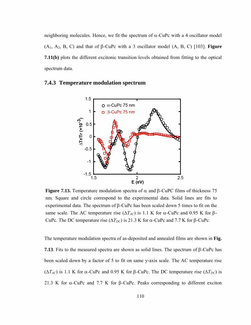
110
neighboring molecules. Hence, we fit the spectrum of α-CuPc with a 4 oscillator model
(A1, A2, B, C) and that of β-CuPc with a 3 oscillator model (A, B, C) [103]. Figure
7.11(b) plots the different excitonic transition levels obtained from fitting to the optical
spectrum data.
7.4.3 Temperature modulation spectrum
The temperature modulation spectra of as-deposited and annealed films are shown in Fig.
7.13. Fits to the measured spectra are shown as solid lines. The spectrum of β-CuPc has
been scaled down by a factor of 5 to fit on same y-axis scale. The AC temperature rise
(ΔTAC) is 1.1 K for α-CuPc and 0.95 K for β-CuPc. The DC temperature rise (ΔTDC) is
21.3 K for α-CuPc and 7.7 K for β-CuPc. Peaks corresponding to different exciton
Figure 7.13. Temperature modulation spectra of α and β-CuPC films of thickness 75 nm. Square and circle correspond to the experimental data. Solid lines are fits to experimental data. The spectrum of β-CuPc has been scaled down 5 times to fit on the same scale. The AC temperature rise (ΔTAC) is 1.1 K for α-CuPc and 0.95 K for β-CuPc. The DC temperature rise (ΔTDC) is 21.3 K for α-CuPc and 7.7 K for β-CuPc.
111
transition energies are visible in the modulation spectrum. For α-CuPc, the first three
peaks (~ 1.65 eV, 1.8 eV and 1.93 eV) and the shoulder at ~ 2.05 eV correspond to the
first 3 Frenkel exciton transitions [103]. The peak at ~ 2.2 eV corresponds to a CT
exciton [103]. For β-CuPc, the first three peaks (~ 1.65 eV, 1.75 eV and 1.9 eV)
correspond to the first 2 exciton transitions, and the peak at 2.05 eV corresponds to a CT
exciton [103]. The modulation spectrum corresponding to the Frenkel exciton states is
larger in β-CuPc than in α-CuPc, while the modulated spectrum of CT excitons is
smaller. The increase in the modulation spectrum of Frenkel states could be because of
increased roughness of the film observed in XRD and AFM data, which leads to an
increase in effective thickness of the film because of light scattering at film surface. A
decrease in the modulation spectrum corresponding to CT excitons is seen for β-CuPc
because of a larger intermolecular spacing along the b-axis as compared to α-CuPc. This
leads to a smaller effect on CT excitonic properties for β-CuPc than α-CuPc upon
applying the same amplitude of temperature modulation.
Because of small intermolecular forces, the separation between the exciton transition
levels is small in molecular crystals (~ 0.1 eV) as compared to inorganic crystals where
the bandgaps are of the order of 1 eV. This leads to a strong overlap between the different
exciton transition levels, leading to a broad absorption spectrum. The temperature
modulation spectrum also shows this effect, and the assignment of peaks to different
exciton transition levels is difficult because of spectral overlaps. In addition, a change in
temperature leads to a shift in exciton transition levels as well as a change in the
oscillator strength and linewidth. Hence, we use a data fitting method based on least
square minimization of error in the calculated temperature modulation spectrum to link
temperature modulation data to different exciton transition levels.
112
To understand the effect of temperature modulation on excitonic properties we
must know the angle between the molecular polarizability and the electric field for each
excitonic transition. Then, using equation (7.10), we can calculate the change in various
electronic properties such as the dipole moment matrix element or the angle between the
molecular plane and substrate. Evaporated CuPc films are formed with molecules stacked
parallel to the substrate, and CT excitons are formed along the nearest neighbor direction,
which is in the plane of the substrate. Hence, Xxi=0 and Epi can be written as:
2 2, 08pi DA i iE NV Eπ= h (7.16)
For CT excitons, the matrix element can be written as ( )2 2, 0 expDA CTV V dβ= − , where β is
the coefficient of exponential decay that characterizes the strength of electron exchange
between the two molecules and d is the equilibrium distance between the molecules [97]
along the b-axis. The dependence of Ep on temperature (T) is then given by:
( ), 0,
, 0,
2 1 1p CT CT
p CT CT
dE dEdN dE dT N dT E dT
β α= + − (7.17)
For Frenkel excitons we make the assumption that all transitions are polarized along
same direction in the plane of the molecule. The molecular plane makes an angle of θ to
the substrate normal. For plane unpolarized light incident perpendicular to the substrate,
the electric field can be written as:
( )ˆF F X Y= +r )
(7.18)
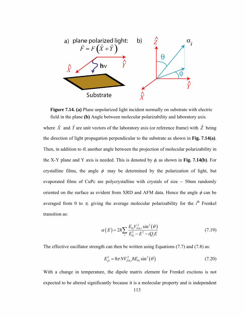
113
where X and Y)
are unit vectors of the laboratory axis (or reference frame) with Z being
the direction of light propagation perpendicular to the substrate as shown in Fig. 7.14(a).
Then, in addition to θ, another angle between the projection of molecular polarizability in
the X-Y plane and Y axis is needed. This is denoted by φ, as shown in Fig. 7.14(b). For
crystalline films, the angle φ may be determined by the polarization of light, but
evaporated films of CuPc are polycrystalline with crystals of size ~ 50nm randomly
oriented on the surface as evident from XRD and AFM data. Hence the angle φ can be
averaged from 0 to π, giving the average molecular polarizability for the ith Frenkel
transition as:
( ) ( )2 20 ,2 20
sin2 i DA i
i i i
E VE
E E iQ Eθ
α =− −∑h (7.19)
The effective oscillator strength can then be written using Equations (7.7) and (7.8) as:
( )2 2 2, 08 sinpi DA i iE NV Eπ θ= h (7.20)
With a change in temperature, the dipole matrix element for Frenkel excitons is not
expected to be altered significantly because it is a molecular property and is independent
Figure 7.14. (a) Plane unpolarized light incident normally on substrate with electric field in the plane (b) Angle between molecular polarizability and laboratory axis.
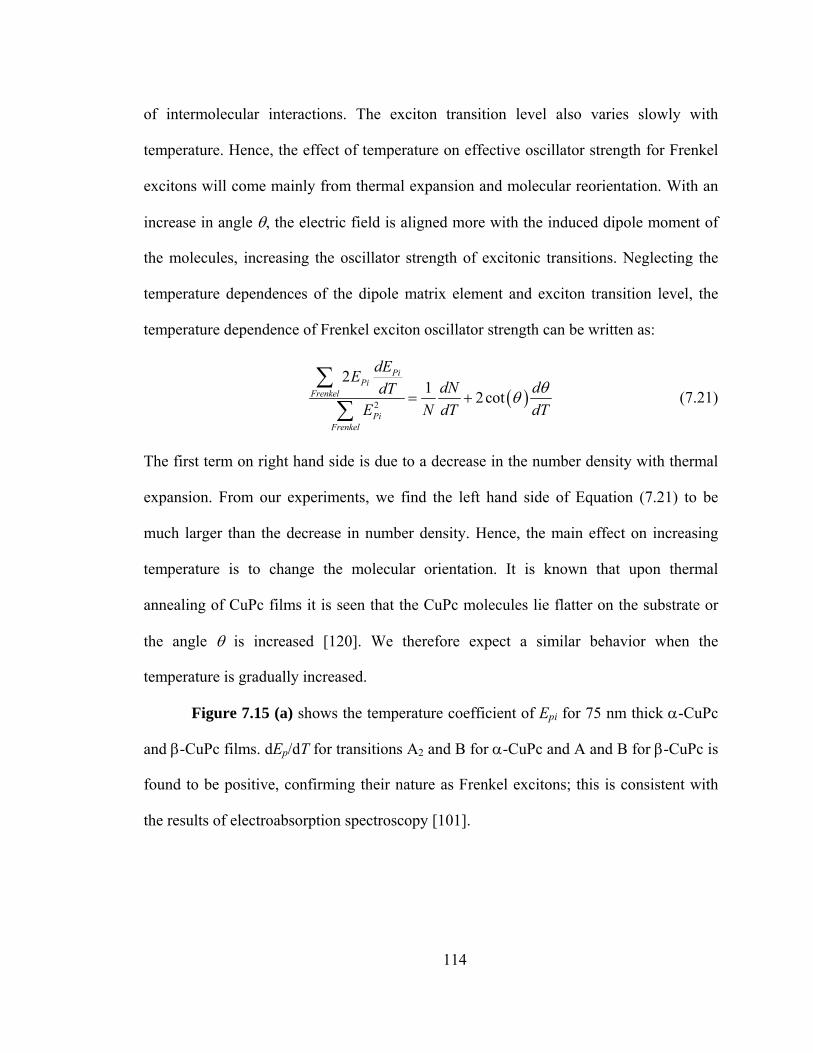
114
of intermolecular interactions. The exciton transition level also varies slowly with
temperature. Hence, the effect of temperature on effective oscillator strength for Frenkel
excitons will come mainly from thermal expansion and molecular reorientation. With an
increase in angle θ, the electric field is aligned more with the induced dipole moment of
the molecules, increasing the oscillator strength of excitonic transitions. Neglecting the
temperature dependences of the dipole matrix element and exciton transition level, the
temperature dependence of Frenkel exciton oscillator strength can be written as:
( )2
21 2cot
PiPi
Frenkel
PiFrenkel
dEEdN ddT
E N dT dTθθ= +
∑∑
(7.21)
The first term on right hand side is due to a decrease in the number density with thermal
expansion. From our experiments, we find the left hand side of Equation (7.21) to be
much larger than the decrease in number density. Hence, the main effect on increasing
temperature is to change the molecular orientation. It is known that upon thermal
annealing of CuPc films it is seen that the CuPc molecules lie flatter on the substrate or
the angle θ is increased [120]. We therefore expect a similar behavior when the
temperature is gradually increased.
Figure 7.15 (a) shows the temperature coefficient of Epi for 75 nm thick α-CuPc
and β-CuPc films. dEp/dT for transitions A2 and B for α-CuPc and A and B for β-CuPc is
found to be positive, confirming their nature as Frenkel excitons; this is consistent with
the results of electroabsorption spectroscopy [101].
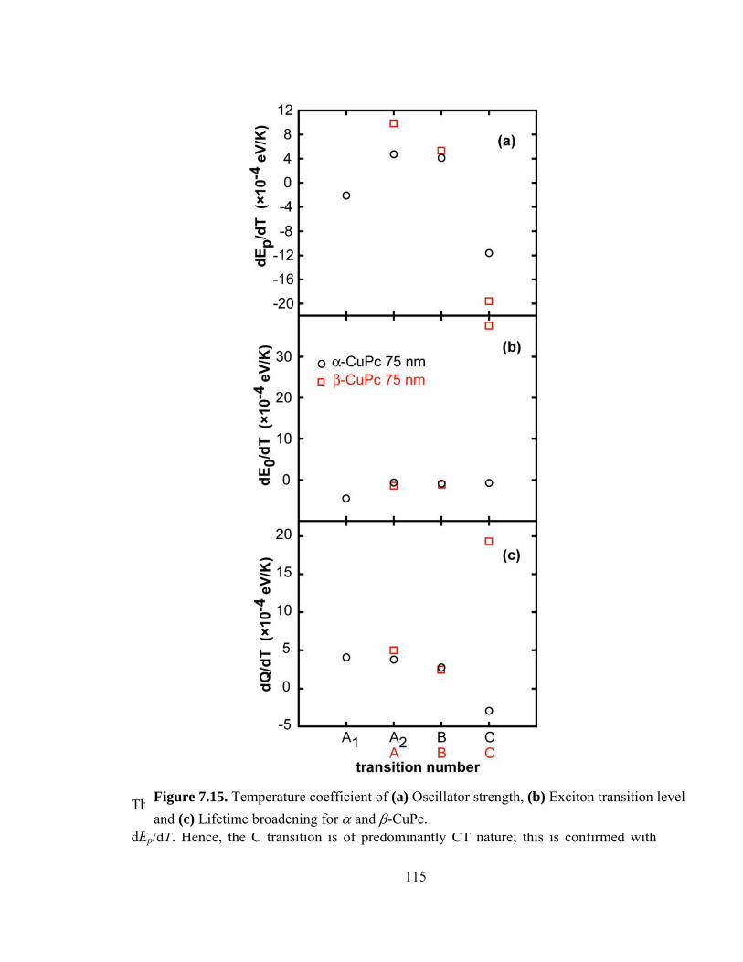
115
The A1 and C transitions for α-CuPc and the C transition for β-CuPc have negative
dEp/dT. Hence, the C transition is of predominantly CT nature; this is confirmed with
Figure 7.15. Temperature coefficient of (a) Oscillator strength, (b) Exciton transition level and (c) Lifetime broadening for α and β-CuPc.
116
electroabsorption spectroscopy [101]. The A1 transition for α-CuPc has a negative dEp/dT
but has been identified as a Frenkel exciton in electroabsorption spectroscopy [101]. We
expect a higher error in resolving the oscillator strength from the transmission spectrum
for the A1 transition in α-CuPc, because of lifetime broadening and its low oscillator
strength. The higher measured dEp/dT for transition C in β-CuPc in comparison to that in
α-CuPc is in contradiction to the measured ΔTr/Tr spectrum, where even a larger
thickness of β-CuPc film has a smaller ΔTr/Tr for the C transition as compared to α-
CuPc. This is mostly likely because a larger equilibrium intermolecular distance along
the stacking axis for β-CuPc leads to Ep for CT excitons being much less sensitive to
changes in intermolecular distance than α-CuPc. This result is in contrast to electric field
modulation, where CT states in β-CuPc are more sensitive to modulation amplitude of
electric field than α-CuPc because of smaller mixing between CT and Frenkel excitons in
β-CuPc, arising from a larger intermolecular distance along the b-axis [103].
Using Equation (7.17) and literature values for the coefficients of linear thermal
expansion (1×10⁻⁴ for α-CuPc and 0.36×10⁻⁴ for β-CuPc [121]), we obtain a value of β of
13.6 Å-1 for α-CuPc and 40.6 Å-1 for β-CuPc. This value is significantly higher than
those measured for LUMO-LUMO charge transfer in frozen media between various
aromatic molecules such as biphenyl-naphthalene [97, 98]. The value of the transfer
integral for HOMO-HOMO charge transfer is 5-10 times lower than LUMO-LUMO
charge transfer, which could arise because of a larger β for HOMO-HOMO charge
transfer [122]. Charge transfer excitons are formed between the HOMO of one molecule
and the LUMO of a neighboring molecule. Because of the difference in energy levels and
the spatial extent of electronic wavefunction between HOMO and LUMO levels, β is
expected to be even larger for the case of charge transfer excitons. A discrepancy
117
between the values of β for α and β-CuPc is also seen, which most likely arises from the
significant difference in thermal expansion coefficient.
The oscillator strength of Frenkel excitons is expected to increase with an increase in
temperature because of an increase in the angle of molecules (θ) with respect to the
substrate normal. The ratio (∑2×Epi×dEpi/dT)/( ∑Epi2) is found to be 8.6 K-1 for α-CuPc
and 18.4 K-1 for β-CuPc. The angle θ is not known with certainty for α and β-CuPc films,
but it is expected to be larger for β-CuPc as evidenced by the smaller distance between
the molecules along the a-axis in β-CuPc in comparison to α-CuPc. If π-π* transitions
are polarized in the plane of molecules, then using Equation (7.21) we find dθ/dT to be
larger for β-CuPc in comparison to α-CuPc. The linear expansion coefficient of β-CuPc
is smaller than α-CuPc. It can be concluded that the relaxation of intermolecular
repulsion on increasing temperature occurs mostly through thermal expansion in α-CuPc
but through molecular reorientation in β-CuPc. The molecules are inclined more in β-
CuPc with respect to the normal to the surface than in α-CuPc. The end to end distance
between neighboring molecules is smaller in α-CuPc, leading to a relatively larger
thermal expansion.
Figure 7.15 (b) shows the temperature coefficients of E0i for the same 75 nm
thick α-CuPc film and 75 nm thick β-CuPc film as discussed above. Similar values of
dE0/dT are obtained for β-CuPc and α-CuPc films, except for transition C for which there
is a significant error in fitting as mentioned earlier. A general trend of E0 to lower
energies is seen. The magnitude of dE0/dT is also found to be smaller than dEp/dT or
dQ/dT. Hence the exciton transition levels are affected to a lesser extent by temperature
than by either oscillator strength or linewidth.
Figure 7.15 (c) shows the temperature coefficient of Qi for the same 75 nm thick
118
α-CuPc film and 75 nm thick β-CuPc film. An increase in the linewidth is seen for
Frenkel excitons in both α and β-CuPc, with the increase in linewidth being larger for
lower energy excitons. The two lowest energy exciton bands have a minimum in the
dispersion at k=0 according to reference [112]. Hence, lifetime broadening can occur only
through the absorption of phonons. With an increase in temperature, phonon occupation
at higher energies is increased, leading to a larger lifetime broadening. For the case of
high energy excitons (B and C), the exciton dispersion shows a maximum at k=0 [112].
Hence, lifetime broadening occurs through the emission of phonons, which is a
temperature independent process. Some increase in broadening is still seen for transition
B, which could be caused by the absorption of phonons resulting from interband
transitions. For the CT excitons, the linewidth shows a decrease for α-CuPc. The CT
excitons in α-CuPc are strongly affected by temperature modulation, which may result in
a decrease in exciton dispersion due to smaller interaction between neighboring
molecules leading to a decrease in linewidth. For the case of β-CuPc there is a significant
error in data fitting for CT excitons as seen in Fig. 3, which gives the erroneous result of
a large increase in linewidth with temperature.
7.5 Summary and Conclusions
In summary, we have used the temperature modulation spectra of α and β-CuPc to
quantify the interband coupling between molecules and differentiate exciton types. A
dielectric model of excitons in conjunction with a least square minimization of error is
used to determine the oscillator strength, exciton transition energy and linewidth from
measured optical transmission. These values are then used to obtain the temperature
coefficients of the oscillator strength, exciton transition energy, and linewidth from the
119
temperature modulation data. The oscillator strength for CT excitons is shown to
decrease as temperature is increased, with the opposite behavior observed for Frenkel
excitons. This criterion can be used to differentiate between Frenkel and CT excitons in
organic semiconductors. The technique is shown to be more sensitive than electric field
modulation spectroscopy for finding CT excitons with strong intermolecular interactions
such as in α-CuPc. A shift in the exciton transition levels to lower energy is seen, but its
magnitude is smaller than the temperature coefficients of oscillator strength and linewidth
broadening. The linewidth increases with an increase in temperature. A larger increase in
the linewidth broadening is seen for lower transition energies, which is attributed to
temperature-dependent phonon absorption based lifetime broadening. In comparison, the
linewidth broadening of higher energy excitons is through the temperature-independent
process of phonon emission.
120
Chapter 8
Conclusions
8.1 Summary of present work The aim of present work is to use thermal effects to understand electronic
structure and transport properties in organic and inorganic semiconductors that play an
important role in determining the efficiencies of thermoelectric and photovoltaic devices.
In addition, innovative thermoelectric device geometries have been examined.
Thermoelectric energy conversion can provide many advantages over traditional
compression cycle based engines or heat pumps, such as low cost, reliability, and small
volume. However, current TE modules suffer from low conversion efficiency. In Chapter
2, we studied the tradeoff between electrical conductivity and Seebeck coefficient, a
primary cause for low efficiency in bulk thermoelectric materials. Nanostructured
materials provide an opportunity to circumvent this tradeoff by independently controlling
the Seebeck coefficient and electrical conductivity. However, while 1D structures such as
nanowires and nanowire superlattices have shown the potential for high ZT, practical
devices based on these structures are plagued by practical difficulties. In Chapter 3, we
examined nanocomposites based on quantum dots that are aligned to form 1D chains as
an alternative method to achieve 1D transport (and consequently high ZT) without the
practical difficulties of nanowires. An increase in the thermoelectric power factor of over
121
5 was predicted for InAs/GaAs quantum dot chains.
In spite of low efficiency, thermoelectric devices have applications in niche areas
where cost or space requirements are important. Two such applications were investigated
in Chapters 4 and 5. In Chapter 4, we demonstrated the feasibility of using monolithically
integrated thermoelectric devices to cool HgCdTe-based infrared detectors. Using a
steady state differential measurement, we measured the Seebeck coefficient and thermal
conductivity of small barrier HgCdTe superlattices, deriving an upper limit for ZT of 1.4.
Chapter 5 examined the feasibility of thermoelectric textiles composed of thin
film thermocouples on fibers. This technology could be suitable for waste heat recovery
applications requiring large area flexible thermoelectric power generators. To
demonstrate the fundamental building block of such a system, Ni-Ag thermocouples were
fabricated on fibers, and thermoelectric power generation was measured. Plain weave
geometries consisting of multiple fibers were also fabricated using a combination of
thermal evaporation and electroless plating. The measured heat transfer coefficient of this
device geometry was used to optimize convectively cooled thermoelectric segments and
extrapolate performance to more high-performance thermoelectric material systems.
In Chapter 7, we studied thermal effects on excitonic properties of organic
semiconductors. Excitons are of fundamental importance for the conversion of light into
electricity in organic semiconductors. Recognizing that temperature affects a material’s
crystal structure by thermal expansion, we developed a phase-sensitive detection
technique to measure the change in a material’s transmission spectrum during
temperature modulation. From the measured change in transmission spectrum for the
organic material CuPc, the temperature derivatives of oscillator strength, exciton
transition level, and lifetime broadening were calculated. The temperature derivative of
122
oscillator strength showed a clear distinction between Frenkel and CT excitons,
demonstrating that the technique could be further applied to study the different
mechanisms within the photovoltaic conversion process associated with these exciton
types.
8.2 Suggestions for future work
8.2.1 Effect of band bending on thermoelectric power factor of metal nanoparticle-semiconductor nanocomposites
In Chapter 3 we examined quantum dot superlattices with unipolar doping. Bipolar
doping or the presence of metal nanoparticles can significantly increase the electronic
band bending at interfaces. It has been shown that the Seebeck coefficient can greatly
increase in the depletion region surrounding an interface [123]. This could potentially be
used to further enhance the thermoelectric performance predicted for quantum dot chains.
8.2.2 Fabrication of thermoelectric materials on plastic substrates
The feasibility of textile-based thermoelectric power generators has been
demonstrated using metal thermocouples. However, the efficiency of such devices could
be greatly increased if thin-film semiconductors with higher ZT (such as chalcogenides)
could be fabricated on plastic substrates. Non-epitaxial growth of semiconductors can be
achieved using vacuum methods such as vacuum thermal evaporation or solution-based
methods such as electrodeposition. Films deposited using these methods are generally
polycrystalline or amorphous, and optimization of annealing conditions are required to
maximize their thermoelectric performance. In addition, surface preparation for
maximizing adhesion is also important. The fabrication processes themselves must be
optimized to obtain good quality films.
123
8.2.3 Stark effect imaging of organic field effect transistors
Stark effect spectroscopy has been used to study excitonic transitions in organic
semiconductors; the change in optical spectrum has been shown to be proportional to
square of the applied electric field. This method could also be used to study the local
electric field in organic semiconductor devices such as thin film transistors. For example,
if a light beam of less than 5μm diameter is scanned across a transistor channel while the
Stark effect spectrum is simultaneously measured using a lock-in technique; the local
electric field can be obtained. This map of the electric field would likely provide useful
information regarding the mechanisms of charge injection.
124
Bibliography
[1] C. Kittel, Introduction to solid state physics (Wiley, New Jersey, 1966).
[2] K. P. Odonnell, and X. Chen, Appl. Phys. Lett. 58, 2924 (1991).
[3] R. F. Pierret, Semiconductor fundamentals (Addison-Wesley, New York, 1983).
[4] G. Chen, Nanoscale Energy Transport and Conversion: A Parallel Treatment of
Electrons, Molecules, Phonons, and Photons (Oxford University Press, New York,
2005).
[5] J. Singh, Electronic and optoelectronic properties of semiconductor structures
(Cambridge University Press, New York, 2003).
[6] H. J. GOLDSMID, Rev. Gen. Therm. 6, 102 (1967).
[7] A. F. Ioffe, Semiconductor Thermoelements and Thermoelectric Cooling
(Infosearch, ltd., London, 1958).
[8] www.melcor.com
[9] S. W. Angrist, Direct energy conversion 1965), p. Medium: X; Size: Pages: 440.
[10] T. M. Tritt, Science 283, 804 (1999).
[11] M. Lundstrom, Fundamentals of Carrier Transport (Cambridge University Press,
Cambridge, 2000), p. 418.
[12] T. C. Harman et al., Science 297, 2229 (2002).
[13] L. D. Hicks et al., Physical Review B 53, 10493 (1996).
125
[14] D. A. Broido, and T. L. Reinecke, Physical Review B 51, 13797 (1995).
[15] D. A. Broido, and T. L. Reinecke, Physical Review B 64, 10 (2001).
[16] Y. M. Lin, X. Z. Sun, and M. S. Dresselhaus, Physical Review B 62, 4610 (2000).
[17] Y. M. Lin, and M. S. Dresselhaus, Physical Review B 68, 14 (2003).
[18] N. Mingo, Appl. Phys. Lett. 84, 2652 (2004).
[19] N. Mingo, Appl. Phys. Lett. 85, 5986 (2004).
[20] A. R. Abramson et al., J. Microelectromech. Syst. 13, 505 (2004).
[21] M. S. Dresselhaus et al., Adv. Mater. 19, 1043 (2007).
[22] D. J. Bergman, and O. Levy, J. Appl. Phys. 70, 6821 (1991).
[23] A. A. Balandin, and O. L. Lazarenkova, Appl. Phys. Lett. 82, 415 (2003).
[24] W. Ye et al., in 32nd Annual Conference on the Physic and Chemistry of
Semiconductor Interfaces (A V S Amer Inst Physics, Bozeman, MT, 2005), pp. 1736.
[25] B. Lita et al., Appl. Phys. Lett. 74, 2824 (1999).
[26] Z. M. Wang et al., Appl. Phys. Lett. 84, 1931 (2004).
[27] T. Mano et al., J. Appl. Phys. 95, 109 (2004).
[28] L. Li et al., Appl. Phys. Lett. 92, 3 (2008).
[29] N. Mingo, and D. A. Broido, Phys. Rev. Lett. 93, 4 (2004).
[30] W. Kim et al., Phys. Rev. Lett. 96, 4 (2006).
[31] B. Yang et al., Appl. Phys. Lett. 80, 1758 (2002).
[32] K. Brunner, Rep. Prog. Phys. 65, 27 (2002).
[33] S. Kiravittaya et al., Nanoscale Res. Lett. 1, 1 (2006).
[34] K. L. Wang et al., Proc. IEEE 95, 1866 (2007).
[35] G. Bastard, Wave mechanics applied to semiconductor heterostructures (Wiley-
Interscience, 1988).
126
[36] M. Califano, and P. Harrison, J. Appl. Phys. 86, 5054 (1999).
[37] O. L. Lazarenkova, and A. A. Balandin, in 6th International on Quantum
Confinement - Nanostructured Materials and Devices, edited by M. Cahay et al.
(Electrochemical Society Inc, San Francisco, Ca, 2001), pp. 238.
[38] S. Tiwari, and D. J. Frank, Appl. Phys. Lett. 60, 630 (1992).
[39] M. Califano, and P. Harrison, J. Appl. Phys. 88, 5870 (2000).
[40] M. A. Cusack, P. R. Briddon, and M. Jaros, Physical Review B 54, R2300 (1996).
[41] M. Grundmann, O. Stier, and D. Bimberg, Physical Review B 52, 11969 (1995).
[42] O. L. Lazarenkova, and A. A. Balandin, Physical Review B 66, 9 (2002).
[43] J. R. Leite et al., in 1st International Conference on Low Dimensional Structures
and Devices (Elsevier Science Sa Lausanne, Singapore, Singapore, 1995), pp. 250.
[44] D. K. C. MacDonald, Thermoelectricity: An Introduction to the Principles (Dover
Publications 2006).
[45] X. Kleber et al., Model. Simul. Mater. Sci. Eng. 13, 341 (2005).
[46] D. Ganapathy, K. Singh, and P. E. Phelan, J. Heat Transf.-Trans. ASME 127, 553
(2005).
[47] A. Wacker, and A. P. Jauho, Phys. Rev. Lett. 80, 369 (1998).
[48] O. L. Lazarenkova, and A. A. Balandin, J. Appl. Phys. 89, 5509 (2001).
[49] A. Rogalski, Infrared detectors (CRC Press, Amsterdam, 2000).
[50] R. W. Miles, in Properties of Mercury Cadmium Telluride, edited by J. Brice, and
P. Caper (INSPEC, New York, 1987), p. 111.
[51] R. J. Radtke, H. Ehrenreich, and C. H. Grein, J. Appl. Phys. 86, 3195 (1999).
[52] D. Vashaee, and A. Shakouri, J. Appl. Phys. 95, 1233 (2004).
[53] D. Vashaee, and A. Shakouri, Appl. Phys. Lett. 88, 3 (2006).
127
[54] G. H. Zeng et al., J. Appl. Phys. 101, 5 (2007).
[55] B. Yang et al., Appl. Phys. Lett. 81, 3588 (2002).
[56] T. Borca-Tasciuc et al., Superlattices Microstruct. 28, 199 (2000).
[57] Y. Zhang et al., in Thermoelectric Materials 2003-Research and Applications,
edited by G. S. Nolas et al. (Materials Research Society, Warrendale, 2004), pp. 59.
[58] J. O. Sofo, G. D. Mahan, and J. Baars, J. Appl. Phys. 76, 2249 (1994).
[59] C. LaBounty et al., Optical Engineering 39, 2847 (2000).
[60] N. K. Dutta et al., Appl. Phys. Lett. 47, 222 (1985).
[61] P. R. Berger et al., Appl. Phys. Lett. 59, 117 (1991).
[62] E. E. Antonova, D. C. Looman, and Ieee, Finite elements for thermoelectric
device analysis in ANSYS (Ieee, New York, 2005), pp. 200.
[63] C. Nui, T. A. S. Srinivas, and H. Ahmed, Microelectromechanical Systems,
Journal of 6, 136 (1997).
[64] S. Velicu et al., J. Electron. Mater. 37, 1504 (2008).
[65] J. Yang, in American Physical Society March Meeting, Energy Workshop, New
Orleans, Louisiana (March 9, 2008).
[66] A. I. Casian, in Thermoelectrics Handbook: Macro to Nano, edited by D. M.
Rowe (CRC Press, London 2006).
[67] C. Lungenschmied et al., Solar Energy Materials and Solar Cells 91, 379 (2007).
[68] B. O'Connor et al., Adv. Mater. 19, 3897 (2007).
[69] J. J. Allen, and A. J. Smits, Journal of Fluids and Structures 15, 629 (2001).
[70] F. Mohammadi, A. Khan, and R. B. Cass, in Symposium on Electronics on
Unconventional Substrates-Electrotextiles and Giant-Area Flexible Circuits held at the
2002 MRS Fall Meeting, edited by M. S. Shur, P. M. Wilson, and D. Urban (Materials
128
Research Society, Boston, Ma, 2002), pp. 263.
[71] J. A. Paradiso, and T. Starner, Pervasive Computing, IEEE 4, 18 (2005).
[72] K. Itoigawa et al., in 4thInternational Workshop on Micro and Nanotechnology
for Power Generation and Energy Conversion Applications (Iop Publishing Ltd, Kyoto,
JAPAN, 2004), pp. S233.
[73] N. Sato, M. Takeda, and Ieee, in 24th International Conference on
Thermoelectrics (ICT) (Ieee, Clemson, SC, 2005), pp. 160.
[74] A. P. Ghosh et al., Appl. Phys. Lett. 86, 223503 (2005).
[75] A. Dhawan et al., in Symposium on Electronics on Unconventional Substrates-
Electrotextiles and Giant-Area Flexible Circuits held at the 2002 MRS Fall Meeting,
edited by M. S. Shur, P. M. Wilson, and D. Urban (Materials Research Society, Boston,
Ma, 2002), pp. 67.
[76] A. R. Horrocks, and S. C. Anand, Handbook of Technical Textiles (Woodhead
Publishing Cambridge, England, 2000).
[77] Syukri et al., Thin Solid Films 422, 48 (2002).
[78] W. Zhang et al., Microelectronic Engineering 76, 146 (2004).
[79] F. J. Blatt et al., Thermoelectric Power of Metals (Plenum press, New York
1976).
[80] S. W. Angrist, Direct Energy Conversion (Allyn and Bacon Inc., Boston 1982).
[81] G. Min, and D. M. Rowe, in CRC Handbook of Thermoelectrics, edited by D. M.
Rowe (CRC Press, London 1995).
[82] D. M. Rowe, and G. Min, Journal of Power Sources 73, 193 (1998).
[83] F. P. I. a. D. P. DeWitt, Fundamentals of Heat & Mass Transfer (John Wiley &
Sons, New York 2002).
129
[84] L. W. d. Silva, M. Kaviany, and C. Uher, J. Appl. Phys. 97, 114903 (2005).
[85] L. M. Goncalves et al., in Thermoelectrics, 2006. ICT '06. 25th International
Conference on2006), pp. 327.
[86] J. L. Bredds, and J. R. Durrant, Accounts Chem. Res. 42, 1689 (2009).
[87] M. Schwoerer, and H. C. Wolf, Organic Molecular Solids (Wiley-VCH, 2007).
[88] http://www.nrel.gov/pv/thin_film/docs/kaz_best_research_cells.ppt
[89] P. Peumans, A. Yakimov, and S. R. Forrest, J. Appl. Phys. 93, 3693 (2003).
[90] S. R. Forrest, Nature 428, 911 (2004).
[91] M. Pope, and C. E. Swenberg, Electronic Processes in Organic Crystals (Oxford
University Press, New York, 1982).
[92] E. A. Silinsh, and V. Capek, Organic Molecular Crystals (AIP Press, New York,
1994).
[93] Y. Vertsimakha et al., Thin Solid Films 515, 7950 (2007).
[94] V. Bulovic, and S. R. Forrest, Chem. Phys. Lett. 238, 88 (1995).
[95] J. L. Bredas et al., Proc. Natl. Acad. Sci. U. S. A. 99, 5804 (2002).
[96] N. Koch et al., Phys. Rev. Lett. 96, 4 (2006).
[97] R. A. Marcus, and N. Sutin, Biochimica Et Biophysica Acta 811, 265 (1985).
[98] J. R. Miller, J. V. Beitz, and R. K. Huddleston, J. Am. Chem. Soc. 106, 5057
(1984).
[99] M. Cardona, Modulation spectroscopy (Academic Press, New York, 1969).
[100] R. K. Willardson, and A. C. Beer, Modulation techniques (Academic Press, New
York, 1972).
[101] L. Sebastian, G. Weiser, and H. Bassler, Chemical Physics 61, 125 (1981).
[102] G. U. Bublitz, and S. G. Boxer, Annual Review Of Physical Chemistry 48, 213
130
(1997).
[103] H. Yoshida, Y. Tokura, and T. Koda, Chemical Physics 109, 375 (1986).
[104] Z. Shen et al., Chem. Phys. Lett. 236, 129 (1995).
[105] W. Stampor, Chemical Physics 305, 77 (2004).
[106] M. Liess et al., Synthetic Metals 102, 1075 (1999).
[107] F. Rohlfing, T. Yamada, and T. Tsutsui, J. Appl. Phys. 86, 4978 (1999).
[108] C. Giebeler et al., Applied Physics Letters 75, 2144 (1999).
[109] W. Stampor, Chemical Physics 334, 216 (2007).
[110] N. W. Ashcroft, and N. D. Mermin, Solid State Physics (Holt, Rinehart and
Winston, New York, 1976).
[111] W. H. Flygare, Molecular Structure and Dynamics (Prentice Hall Englewood
Cliffs, NJ.
[112] Y. Iyechika, K. Yakushi, and H. Kuroda, Chemical Physics 87, 101 (1984).
[113] P. K. L. Chan et al., Appl. Phys. Lett. 89, 011110 (2006).
[114] R. Rosei, C. H. Culp, and J. H. Weaver, Physical Review B 10, 484 (1974).
[115] L. T. Harrison, Current Sources and Voltage References (Elseiver, New York,
2005).
[116] R. Rosei, Antonang.F, and U. M. Grassano, Surf. Sci. 37, 689 (1973).
[117] O. Berger et al., Journal Of Materials Science-Materials In Electronics 11, 331
(2000).
[118] M. Tanaka et al., Journal Of Chemical Physics 95, 2371 (1991).
[119] E. A. Lucia, and F. D. Verderame, The Journal of Chemical Physics 48, 2674
(1968).
[120] S. Dogo et al., Thin Solid Films 219, 244 (1992).
131
[121] C. Hamann, and M. Schenk, Kristall und Technik 6, K103 (1971).
[122] J. Kjelstrup-Hansen et al., Organic Electronics 10, 1228 (2009).
[123] K. P. Pipe, Bipolar thermoelectric devices, PhD Thesis (Massachusetts Institute of
Technology, Boston, 2004)