Norbert Koch: Energy materials for electronics and optoelectronic.
13
Research in Germany: Berlin - Adlershof Institut für Physik & IRIS Adlershof Humboldt-Universität zu Berlin Helmholtz Zentrum Berlin für Materialien und Energie GmbH Norbert Koch [email protected] energy materials for electronics & optoelectronics
-
Upload
sociedade-brasileira-de-pesquisa-em-materiais -
Category
Science
-
view
83 -
download
2
Transcript of Norbert Koch: Energy materials for electronics and optoelectronic.

Research in Germany:Berlin - Adlershof
Institut für Physik & IRIS AdlershofHumboldt-Universität zu Berlin
Helmholtz Zentrum Berlinfür Materialien und Energie GmbH
Norbert [email protected]
energy materials for electronics & optoelectronics

Humboldt-Universität zu Berlin
one of Germany’s top research universities
39.000 students
6.000 students from abroad
over 450 tenured faculty members
all main disciplines of humanities,
social and cultural sciences, human medicine,
mathematics & natural sciences

HZB: one center - two sources
annual budget: 110 million Euro
staff: 1.100
scientists: 400
international users: more than 3.000 p.a.
500 2.500
Science with
Neutrons
Science with
PhotonsUser Service
Solar Energy
Research
Energy Materials
Research

Berlin - Adlershof Science & Technology Park
Berlin
one of the 15 biggest science parks worldwide
6 departments of Humboldt-Universität 10 non-university research institutes over 500 technology orientated companies
6.500 students 16.000 employees
annual turnoverin science & technology:1 billion Euro
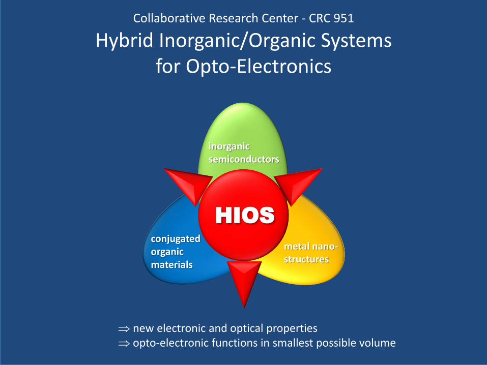
Collaborative Research Center - CRC 951
Hybrid Inorganic/Organic Systemsfor Opto-Electronics
HIOS
inorganic semiconductors
metal nano-structures
conjugated organic materials
new electronic and optical properties opto-electronic functions in smallest possible volume

inorganic semiconductors
highest purity levels high excitation density high carrier mobility
Synergy rationale
• combine & take advantage of individual material strengths• compensate weaknesses
conjugated organicmaterials
tunable energy range strong light-matter coupling high frequency response
metal nanostructures
confine guide emit amplify
light at subwavelength dimensions
• new opto-electronic properties via hybridization

Structure & electronic properties
inorganic semiconductor
conjugated organic material
interface energy levels
VBM
CBM
HOMO
LUMO
VBM
CBM
HOMO
LUMO
hybrid material
reality

Optical excitations
-+
Wannier-Mott Frenkel
-
+
?Tailor optical excitation dynamics:
• energy transfer vs. charge transfer• (non-)radiative decay, mobile carriers
excited state hybridization Exploit hybrid excitations
• formation mechanisms• electronic & spatial structure
- +?

--
-
++
+
metallic/dielectric structures:
• coupling of molecular & hybrid excitations with tailored plasmon polaritons /cavities
Plasmonic & photonic coupling
metal nanostructures:
• local increase - absorption / emission- energy transfer
- +

The CRC 951
• 27 PIs & 60 postdocs/students provide complementary expertise in physics and chemistry of semiconductors & molecular systems, optics/photonics, and inorganic & organic opto-electronics
• all relevant methods in theory and experiment for all three material classes
synergistic merger of scientific communities = added value
FHI
www.physik.hu-berlin.de/sfb951

Inorganic surface work function tuning with donors & acceptors:
Unprecedented dynamic rangeCN
CN
F
F
F
F
NC
NC
not limited to ZnO!
Schlesinger, et al., Phys. Rev. B 87 (2013) 155311Schlesinger, et al., Nat. Commun. 6 (2015) 6754Akaike, et al., Adv. Funct. Mater. 26 (2016) 2493

Functionality of hybrid structure with optimized energy levels
PL emission from L4P-sp3 in hybrid
overall PL yield from 5% to 35%
type-I energy levels realized:•efficient energy transfer•electron transfer from L4P-sp3 exciton to ZnO suppressed
Schlesinger, Bianchi, Blumstengel, Christodoulou, Ovsyannikov, Kobin, Moudgil, Barlow, Hecht, Marder, Henneberger, Koch, Nat. Commun. 6 (2015) 6754
2.8 2.9 3.0 3.1 3.2 3.3
PL
Inte
nsity
Energy (eV)

Rendering: Nickl & Partner Architekten AG
The IRIS Research Building @ Campus Adlershof …
… always ready for new cooperations!


![Organic Electronic Devices and Their Functional Interfacespeople.physik.hu-berlin.de/~nkoch/1.pdf · 2007-07-05 · Norbert Koch*[a] 1. Introduction ... design concepts for consumer](https://static.fdocuments.in/doc/165x107/5f4729e43264fa24cf6ba288/organic-electronic-devices-and-their-functional-nkoch1pdf-2007-07-05-norbert.jpg)