MOSFET Models - SCU · 4-March-04 HO #18: ELEN 251 - MOSFET Models Saha #4 Level-1 MOSFET Model n+...
42
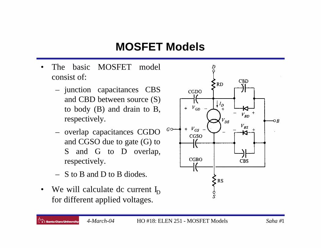
4-March-04 HO #18: ELEN 251 - MOSFET Models Saha # 1 MOSFET Models • The basic MOSFET model consist of: – junction capacitances CBS and CBD between source (S) to body (B) and drain to B, respectively. – overlap capacitances CGDO and CGSO due to gate (G) to S and G to D overlap, respectively. – S to B and D to B diodes. • We will calculate dc current I D for different applied voltages.
Transcript of MOSFET Models - SCU · 4-March-04 HO #18: ELEN 251 - MOSFET Models Saha #4 Level-1 MOSFET Model n+...
4-March-04 HO #18: ELEN 251 - MOSFET Models Saha #1
MOSFET Models
• The basic MOSFET modelconsist of:
– junction capacitances CBSand CBD between source (S)to body (B) and drain to B,respectively.
– overlap capacitances CGDOand CGSO due to gate (G) toS and G to D overlap,respectively.
– S to B and D to B diodes.
• We will calculate dc current IDfor different applied voltages.
4-March-04 HO #18: ELEN 251 - MOSFET Models Saha #2
MOSFET DC Models
Where,
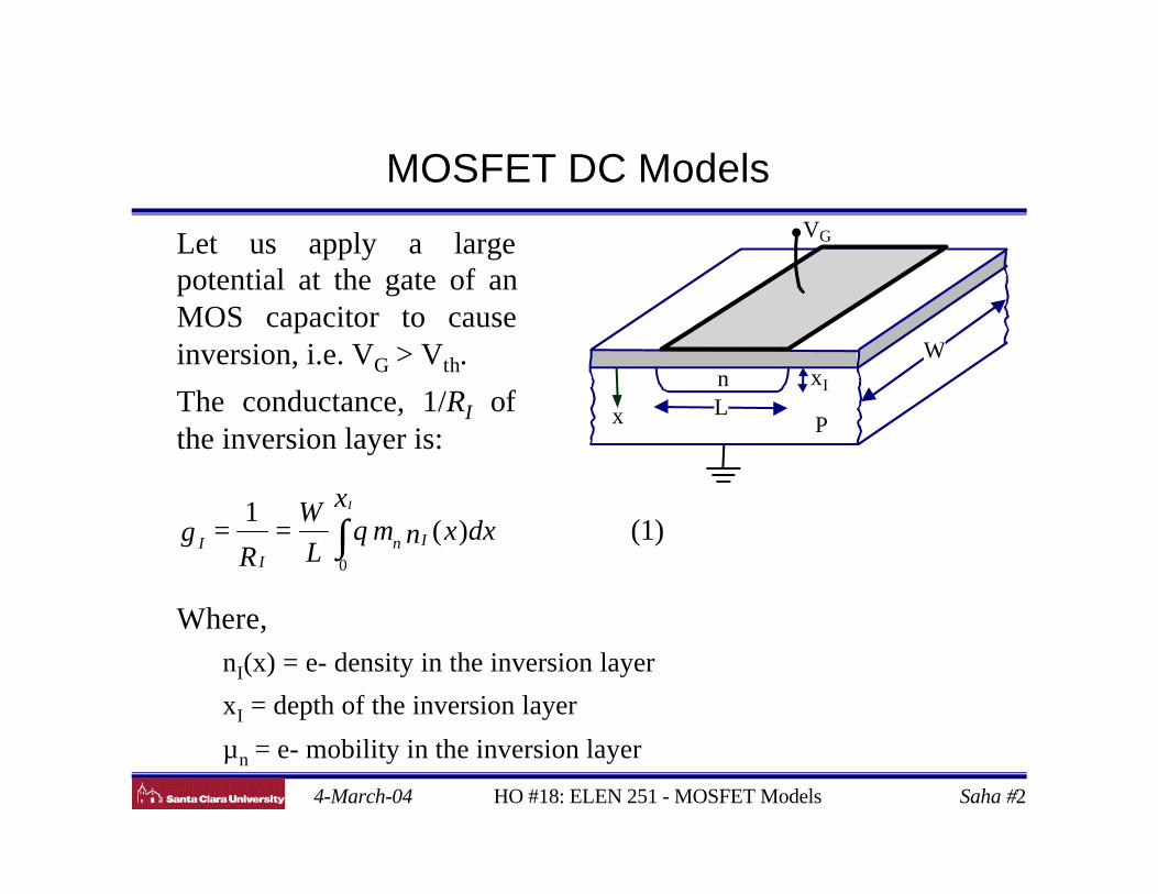
nI(x) = e- density in the inversion layer
xI = depth of the inversion layer
µn = e- mobility in the inversion layer
n
VG
Lx
W
P
xI
Let us apply a largepotential at the gate of anMOS capacitor to causeinversion, i.e. VG > Vth.
The conductance, 1/RI ofthe inversion layer is:
dxxnx
qL
W
Rg In
II
I
)(1
0∫== µ (1)
4-March-04 HO #18: ELEN 251 - MOSFET Models Saha #3
Inversion Layer Conductance
The inversion layer mobility is, also, called the surface mobilityand is ≈ 1/2 bulk mobility.
Now, the inversion layer charge per unit area is given by:
Assuming µn = constant, we get from (1) and (2):
and the inversion layer resistance of an elemental length dy is:
Eq. (4) for MOS capacitors can be directly used to derive draincurrent for MOSFETs under different biasing conditions.
dxxnx
qQ II
I
)(0∫−= (2)
QL
Wg InI µ= (3)(− ⇒ e−)
QW
dydR
In
I µ= (4)
4-March-04 HO #18: ELEN 251 - MOSFET Models Saha #4
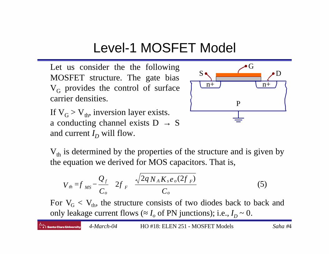
Level-1 MOSFET Model
n+ n+
S DG
P
Let us consider the the followingMOSFET structure. The gate biasVG provides the control of surfacecarrier densities.
If VG > Vth, inversion layer exists. ∴a conducting channel exists D → Sand current ID will flow.
Vth is determined by the properties of the structure and is given bythe equation we derived for MOS capacitors. That is,
For VG < Vth, the structure consists of two diodes back to back andonly leakage current flows (≈ Io of PN junctions); i.e., ID ~ 0.
C
KNq
C
QV
o
FosA
Fo
fMSth
)2(22
φεφφ ++−= (5)
4-March-04 HO #18: ELEN 251 - MOSFET Models Saha #5
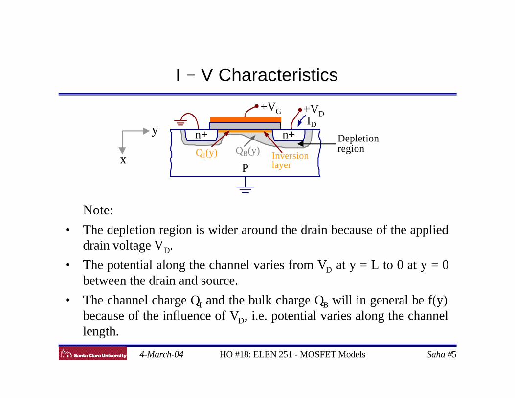
I − V Characteristics
Note:
• The depletion region is wider around the drain because of the applieddrain voltage VD.
• The potential along the channel varies from VD at y = L to 0 at y = 0between the drain and source.
• The channel charge QI and the bulk charge QB will in general be f(y)because of the influence of VD, i.e. potential varies along the channellength.
+VD+VG
P
ID
QI(y) QB(y)
n+ n+
Inversionlayer
Depletionregion
y
x
4-March-04 HO #18: ELEN 251 - MOSFET Models Saha #6
I − V Characteristics
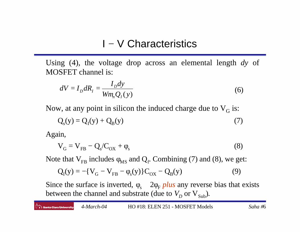
Using (4), the voltage drop across an elemental length dy ofMOSFET channel is:
Now, at any point in silicon the induced charge due to VG is:
Qs(y) = QI(y) + QB(y) (7)
Again,
VG = VFB − Qs/COX + φs (8)
Note that VFB includes φMS and Qf. Combining (7) and (8), we get:
QI(y) = −{VG − VFB − φs(y)}COX − QB(y) (9)
Since the surface is inverted, φs ≅ 2φF plus any reverse bias that existsbetween the channel and substrate (due to VD or VSub).
)( yQW
dyIdRIdV
In
DID µ
== (6)
4-March-04 HO #18: ELEN 251 - MOSFET Models Saha #7
I − V Characteristics
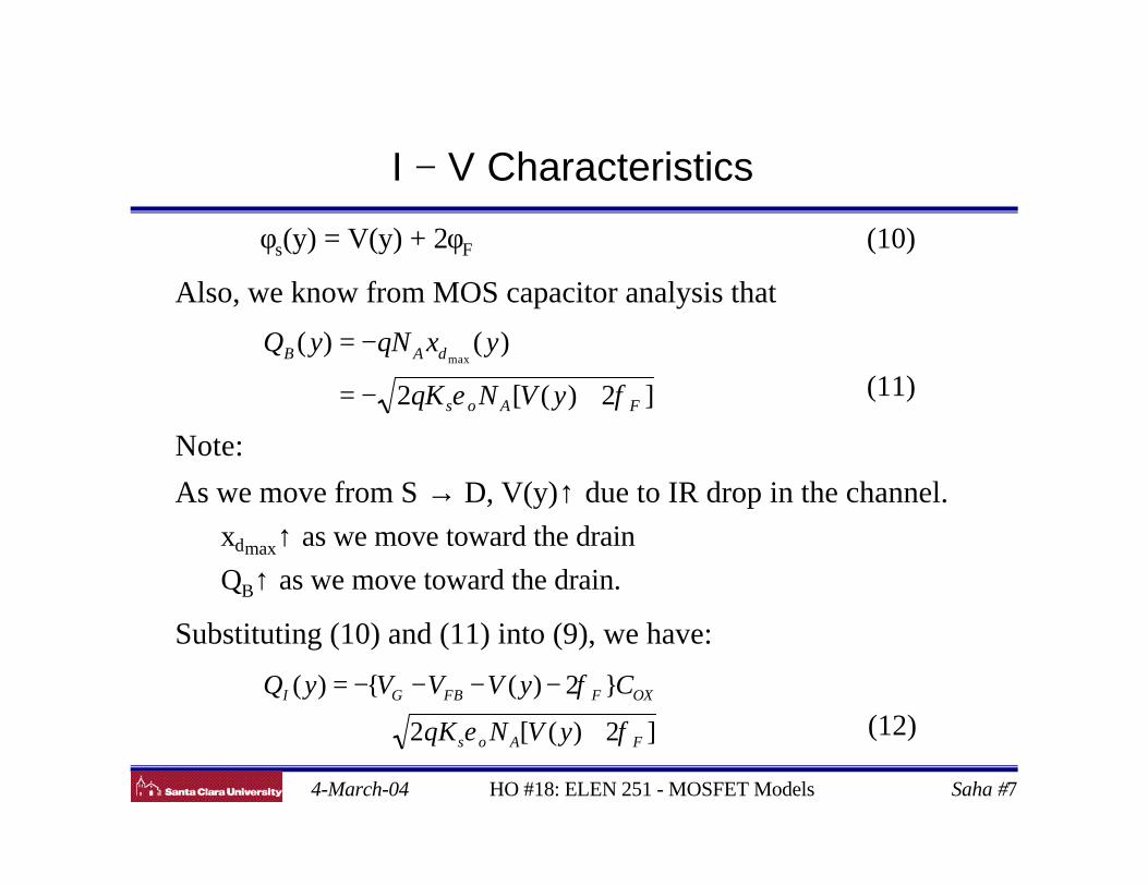
∴ φs(y) = V(y) + 2φF (10)
Also, we know from MOS capacitor analysis that
Note:
As we move from S → D, V(y)↑ due to IR drop in the channel.
∴ xdmax↑ as we move toward the drain
QB↑ as we move toward the drain.
Substituting (10) and (11) into (9), we have:
]2)([2
)()(max
FAos
dAB
yVNqK
yxqNyQ
φε +−=
−=
(11)
]2)([2
}2)({)(
FAos
OXFFBGI
yVNqK
CyVVVyQ
φε
φ
++
−−−−=(12)
4-March-04 HO #18: ELEN 251 - MOSFET Models Saha #8
I − V Characteristics
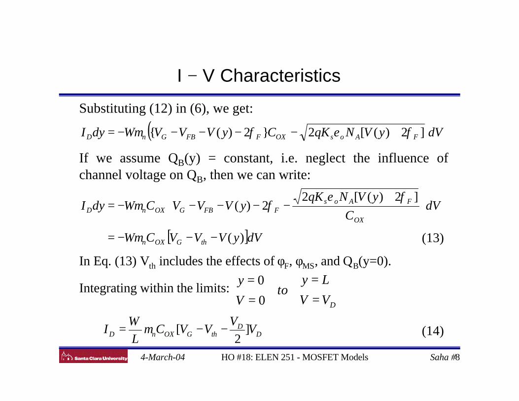
Substituting (12) in (6), we get:
If we assume QB(y) = constant, i.e. neglect the influence ofchannel voltage on QB, then we can write:
In Eq. (13) Vth includes the effects of φF, φMS, and QB(y=0).
Integrating within the limits:
( )dVyVNqKCyVVVWdyI FAosOXFFBGnD ]2)([2}2)({ φεφµ +−−−−−=
(13)[ ]dVyVVVCW
dVC
yVNqKyVVVCWdyI
thGOXn
OX
FAosFFBGOXnD
)(
]2)([22)(
−−−=
+−−−−−=
µ
φεφµ
⇒
==
==
DVV
Lyto
V
y
0
0
DD
thGOXnD VV
VVCL
WI ]
2[ −−= µ (14)
4-March-04 HO #18: ELEN 251 - MOSFET Models Saha #9
I − V Characteristics: Linear Region
Eq. (14) is used in Level 1 MOSFET SPICE model to calculate ID.If we define:
κ ≡ µnCOX = process transconductance
β ≡ µnCOX(W/L) = κ(W/L) = gain factor of the device
If VD < 0.1 V, we can simplify (15) to:
Eq. (16) shows that current varies linearly with VD. This region ofMOSFET operation is called the linear region of operation. From(16), the effective resistance between the source and drain is:
(15)DD
thGD VV
VVI ]2
[ −−= β
(16)( ) DthGD VVVI −≅ β
(17)( )thGD
Dch VVI
VR
−≅=
β1
4-March-04 HO #18: ELEN 251 - MOSFET Models Saha #10
I − V Characteristics
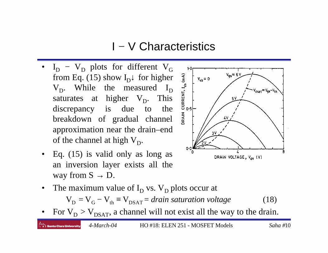
• ID − VD plots for different VG
from Eq. (15) show ID↓ for higherVD. While the measured ID
saturates at higher VD. Thisdiscrepancy is due to thebreakdown of gradual channelapproximation near the drain–endof the channel at high VD.
• Eq. (15) is valid only as long asan inversion layer exists all theway from S → D.
• The maximum value of ID vs. VD plots occur atVD = VG − Vth ≡ VDSAT = drain saturation voltage (18)
• For VD > VDSAT, a channel will not exist all the way to the drain.
4-March-04 HO #18: ELEN 251 - MOSFET Models Saha #11
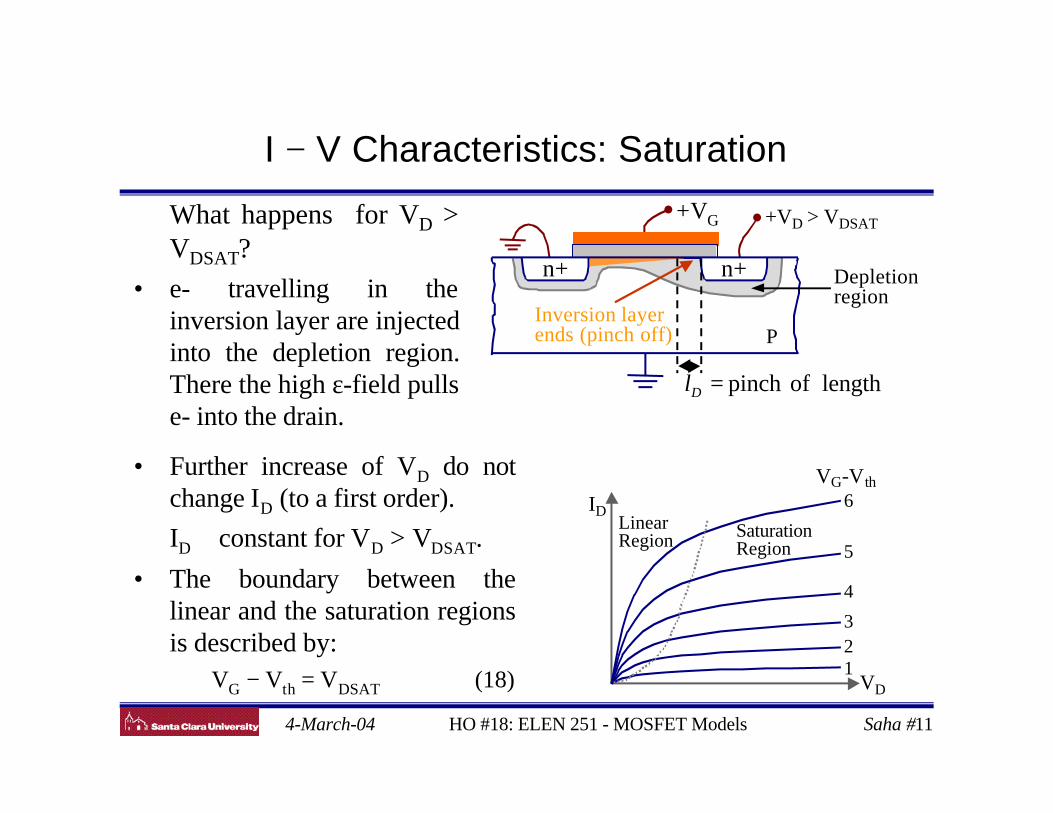
I − V Characteristics: Saturation
What happens for VD >VDSAT?
• e- travelling in theinversion layer are injectedinto the depletion region.There the high ε-field pullse- into the drain.
VD
ID6
5
4
321
VG-Vth
LinearRegion Saturation
Region
• Further increase of VD do notchange ID (to a first order).
∴ ID ≅ constant for VD > VDSAT.
• The boundary between thelinear and the saturation regionsis described by: VG − Vth = VDSAT (18)
+VD > VDSAT+VG
P
n+
Inversion layerends (pinch off)
Depletionregion
n+
lengthofpinch=Dl
4-March-04 HO #18: ELEN 251 - MOSFET Models Saha #12
I − V Characteristics: Saturation
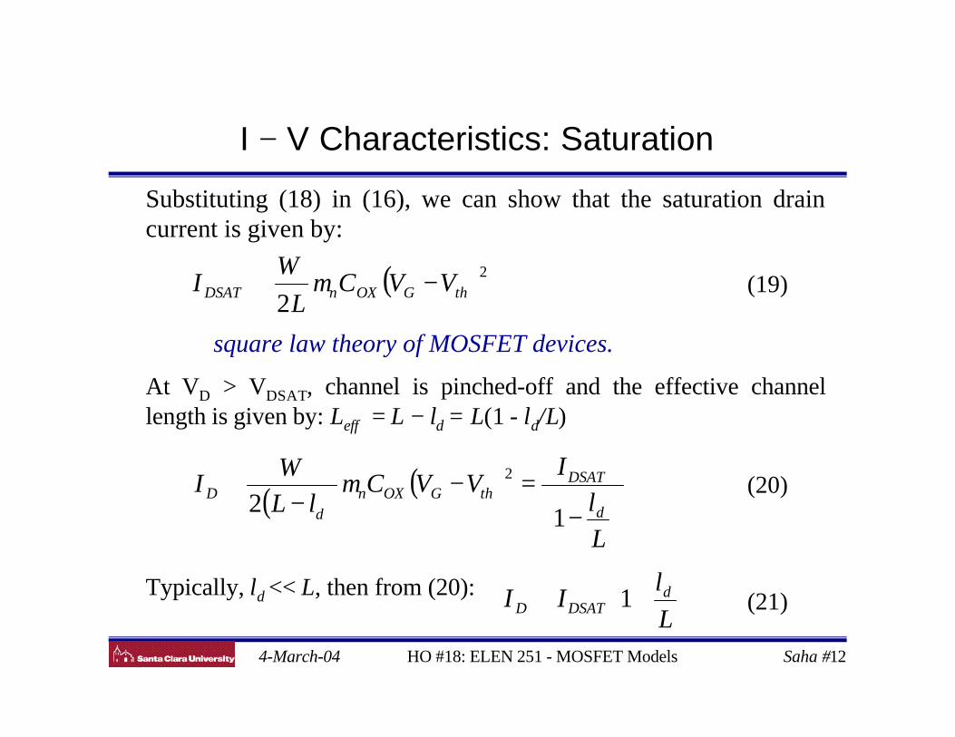
Substituting (18) in (16), we can show that the saturation draincurrent is given by:
⇒ square law theory of MOSFET devices.
At VD > VDSAT, channel is pinched-off and the effective channellength is given by: Leff = L − ld = L(1 - ld/L)
Typically, ld << L, then from (20):
( )2
2 thGOXnDSAT VVCL
WI −≅ µ (19)
( ) ( )
−
=−−
≅∴
Ll
IVVC
lLW
Id
DSATthGOXn
dD
122µ (20)
+≅
L
lII d
DSATD 1 (21)
4-March-04 HO #18: ELEN 251 - MOSFET Models Saha #13
I − V Characteristics: Saturation
Since ld = f(VD), we can write:
Here, λ = f(VD) = channel length modulation model parameter.
Dd VL
lλ+≡+ 11 (22)
( )DDSATD VII λ+≅∴ 1 (23)
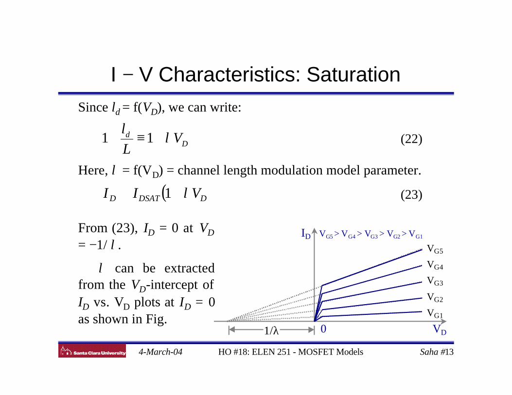
From (23), ID = 0 at VD
= −1/ λ.
∴ λ can be extractedfrom the VD-intercept ofID vs. VD plots at ID = 0as shown in Fig.
VG5
VG4
VG3
VG2
VG1
1/λ VD
ID VG5 > VG4 > VG3 > VG2 > VG1
0
4-March-04 HO #18: ELEN 251 - MOSFET Models Saha #14
Level 1 MOSFET Model: Summary
• Current Eq:
• Model Parameters:
– VTO = threshold voltage at VB = 0
– KP = process transconductance
– GAMMA = body factor
– LAMBDA = channel length modulation factor
– PHI = 2|φF| = bulk Fermi-potential.
(24)
( ) ( ).12
]2
[
0
2DthG
DD
thG
VVV
VV
VV
λβ
β
+−
−−
VG ≤ Vth (cut-off region)
VG ≥ Vth, VD ≤ VDSAT (linear region)
VG ≥ Vth, VD ≥ VDSAT (saturation region)
=DI
4-March-04 HO #18: ELEN 251 - MOSFET Models Saha #15
Level 1 MOSFET Model: Summary
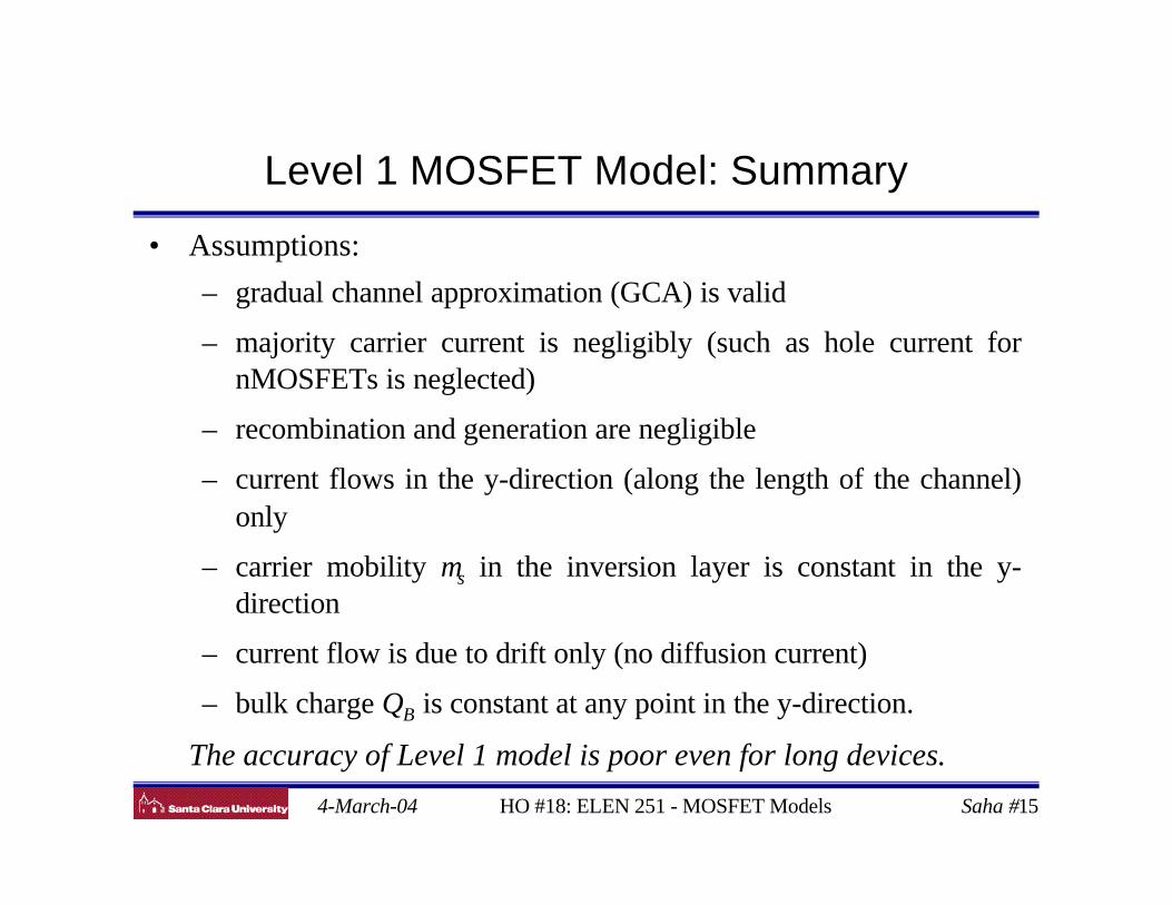
• Assumptions:
– gradual channel approximation (GCA) is valid
– majority carrier current is negligibly (such as hole current fornMOSFETs is neglected)
– recombination and generation are negligible
– current flows in the y-direction (along the length of the channel)only
– carrier mobility µs in the inversion layer is constant in the y-direction
– current flow is due to drift only (no diffusion current)
– bulk charge QB is constant at any point in the y-direction.
The accuracy of Level 1 model is poor even for long devices.

4-March-04 HO #18: ELEN 251 - MOSFET Models Saha #16
Level 2 Model: Bulk-Charge Model
In reality, QB varies along the channel form source at y = 0 todrain at y = L because of applied bias VD. Then from (11) withback bias VB we have:
Using (26) in (6) and integrating form y = 0 to y = L we get:
Eq (27) is the current used by SPICE Level 2 MOSFET model.
)(2
]2)([2)()(max
yVVC
VyVNqKyxqNyQ
BFOX
BFAosdAB
++−=
++−=−=
φγ
φε
(25)
( ))(2)(2)( yVVyVVVCyQ BFFFBGOXI ++−−−−−=∴ φγφ (26)
( ) ( ) }]22{32
)2
2[(
2323BFBFD
DD
FFBGOXn
D
VVV
VV
VVL
CWI
+−++−
−−−=
φφγ
φµ
(27)
4-March-04 HO #18: ELEN 251 - MOSFET Models Saha #17
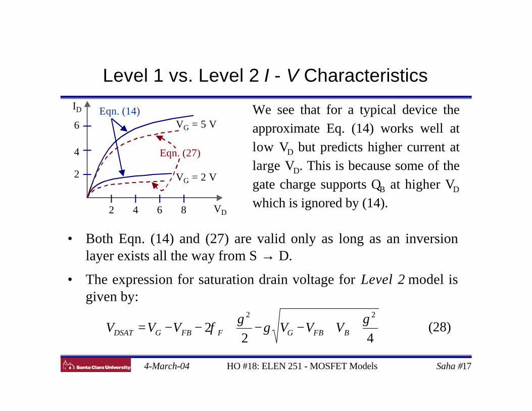
Level 1 vs. Level 2 I - V Characteristics
We see that for a typical device theapproximate Eq. (14) works well atlow VD but predicts higher current atlarge VD. This is because some of thegate charge supports QB at higher VD
which is ignored by (14).
VG = 5 V
VG = 2 V
2 4 6 8
6
4
2
Eqn. (14)
Eqn. (27)
VD
ID
• Both Eqn. (14) and (27) are valid only as long as an inversionlayer exists all the way from S → D.
• The expression for saturation drain voltage for Level 2 model isgiven by:
422
22 γγ
γφ ++−−+−−= BFBGFFBGDSAT VVVVVV (28)

4-March-04 HO #18: ELEN 251 - MOSFET Models Saha #18
Level 2 MOSFET Model Current
• Consideration of QB variation along the channel offers moreaccurate ID modeling in the linear and saturation region.
• The current given by (27) is accurate, however, complex.
∴ ID is simplified using a new model parameters:
• If
(31)( ) ( ).1
2
]2
[
0
2DthG
DD
thG
VVV
VV
VV
λαβ
αβ
+−
−−
VG ≤ Vth (cut-off region)
VG ≥ Vth, VD ≤ VDSAT (linear region)
VG ≥ Vth, VD ≥ VDSAT (saturation region)
=DI
BF V+=
φδ
2
5.0(29)
then,1 δγα +≡ (30)
4-March-04 HO #18: ELEN 251 - MOSFET Models Saha #19
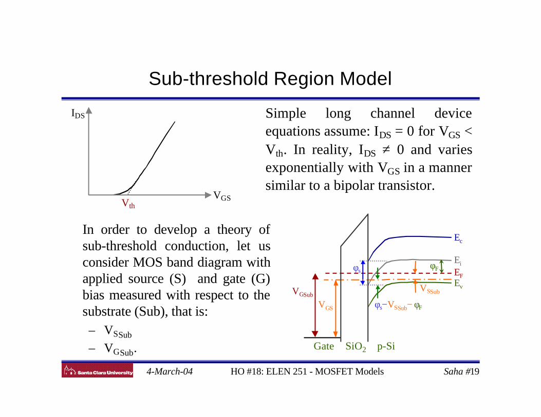
Sub-threshold Region Model
Simple long channel deviceequations assume: IDS = 0 for VGS <Vth. In reality, IDS ≠ 0 and variesexponentially with VGS in a mannersimilar to a bipolar transistor.
IDS
VGSVth
In order to develop a theory ofsub-threshold conduction, let usconsider MOS band diagram withapplied source (S) and gate (G)bias measured with respect to thesubstrate (Sub), that is:– VSSub
– VGSub.
Ev
EF
Gate SiO2 p-Si
Eiφs
VGS
Ec
φF
VSSubVGSub
φs−VSSub− φF
4-March-04 HO #18: ELEN 251 - MOSFET Models Saha #20
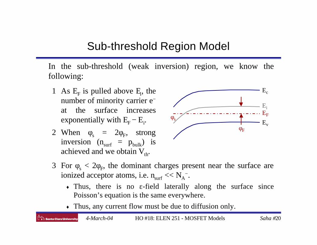
Sub-threshold Region Model
In the sub-threshold (weak inversion) region, we know thefollowing:
Ec
EiEF
EvφF
φs
1 As EF is pulled above Ei, thenumber of minority carrier e−
at the surface increasesexponentially with EF − Ei.
2 When φs = 2φF, stronginversion (nsurf = pbulk) isachieved and we obtain Vth.
3 For φs < 2φF, the dominant charges present near the surface areionized acceptor atoms, i.e. nsurf << NA
−.♦ Thus, there is no ε-field laterally along the surface since
Poisson’s equation is the same everywhere.
♦ Thus, any current flow must be due to diffusion only.
4-March-04 HO #18: ELEN 251 - MOSFET Models Saha #21
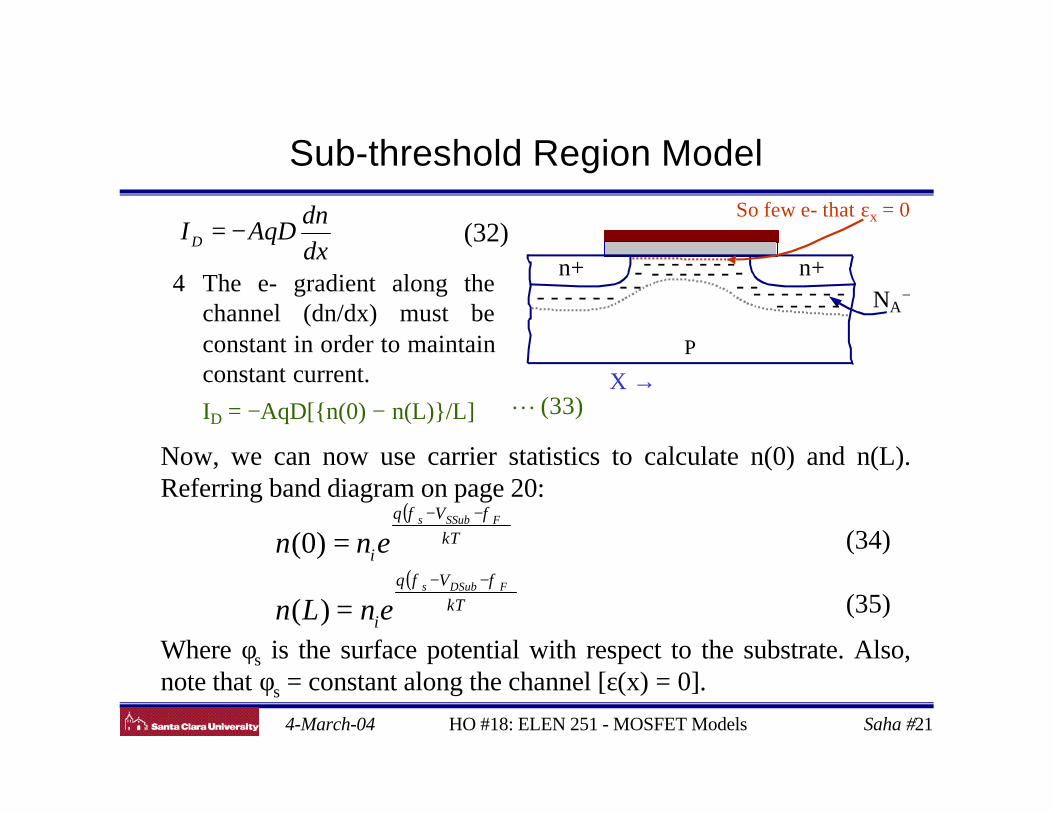
Now, we can now use carrier statistics to calculate n(0) and n(L).Referring band diagram on page 20:
Where φs is the surface potential with respect to the substrate. Also,note that φs = constant along the channel [ε(x) = 0].
Sub-threshold Region Model
n+
P
n+- - - - - - -
- - - - - - - - - - - - -- - - - - --
- --- -
X →
NA−- - - - -
So few e- that εx = 0
dx
dnAqDID −=∴ (32)
4 The e- gradient along thechannel (dn/dx) must beconstant in order to maintainconstant current.
∴ ID = −AqD[{n(0) − n(L)}/L] . . . (33)
( )
( )kT
Vq
i
kT
Vq
i
FDSubs
FSSubs
enLn
ennφφ
φφ
−−
−−
=
=
)(
)0( (34)
(35)

4-March-04 HO #18: ELEN 251 - MOSFET Models Saha #22
Sub-threshold Region Model
Since the charge in the substrate is assumed uniform (NA−), then
from Poisson’s equation:
∴ φ varies parabolically and E varies linearly with distance. Since the e- concentration falls off as e−qφ/kT away from the
surface, essentially, all of the minority carrier e- are contained in aregion in which the potential drops by kT/q.
∴ The depth of the inversion layer, Xinv = ∆φ/Es.where ∆φ = kT/q, and Es is the ε-field at the surface.
Again, from Gauss’ Law:
dx
dEqN
dx
d
s
A −==ε
φ2
2
(36)
sAsBss qNQE φεε 2=−= (37)
sA
s
sAs
s
inv qNq
kT
qN
qkT
Xφ
εφε
ε
22==∴ (38)

4-March-04 HO #18: ELEN 251 - MOSFET Models Saha #23
Sub-threshold Region Model
Using (34), (35), and (38) in (33), we get:
Here A = WXinv.
Using VDSub = VDS + VSSub,
To make use of this equation, we need to know how φs varies withthe externally applied potential VG.
( ) ( )
sA
skT
Vq
kT
Vq
iD qNq
kTeeDn
L
WqI
FDSubsFSSubs
φεφφφφ
2
−=−−−−
(39)
( )
−
=−
−−kT
qV
kT
Vq
sA
siD
DSFSSubs
eeqN
kTDnL
WI 1
2
φφ
φε
(40)
o
sAssFBGSub C
NqVV
φεφ
2++= (41)
4-March-04 HO #18: ELEN 251 - MOSFET Models Saha #24
Sub-threshold Region Model
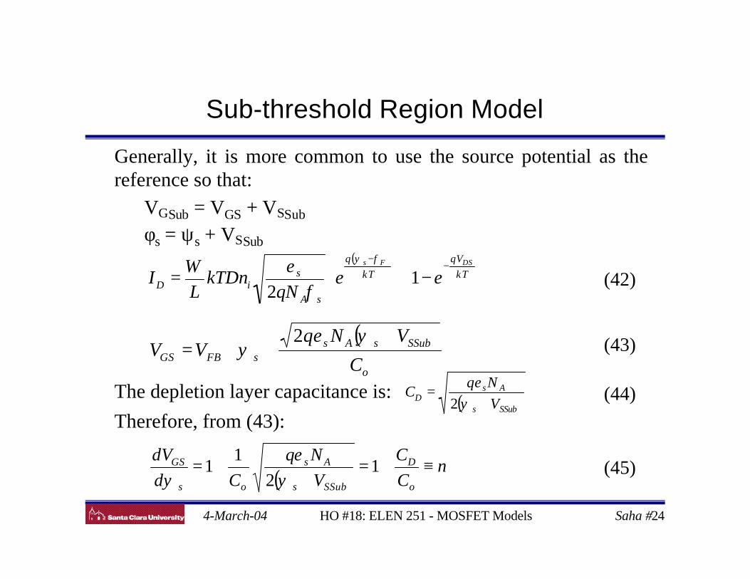
Generally, it is more common to use the source potential as thereference so that:
VGSub = VGS + VSSub
φs = ψs + VSSub
The depletion layer capacitance is:
Therefore, from (43):
( )
−
=∴−
−kT
qV
kT
q
sA
siD
DSFs
eeqN
kTDnL
WI 1
2
φψ
φε
(42)
( )o
SSubsAssFBGS C
VNqVV
+++=
ψεψ
2 (43)
( )SSubs
AsD V
NqC
+=
ψε
2(44)
( ) nC
C
V
Nq
Cd
dV
o
D
SSubs
As
os
GS ≡+=+
+= 12
11
ψε
ψ(45)

4-March-04 HO #18: ELEN 251 - MOSFET Models Saha #25
Sub-threshold Region Model
In order to eliminate ψs from (42), we expand VGS in a seriesabout the point ψs = 1.5φF (weak inversion corresponds to φF ≤ ψs
≤ 2φF).
Where and is obtained from (43).
Combining (46) with (42) to eliminate ψs in the exponential andusing (44) to eliminate the square root of ψs in (42), we obtain:
FsGSGS VV
φψ 5.1
*
=≡
( )FsGSGS nVVFs
φψφψ
5.15.1
−+≅∴= (46)
( )
−
=
−
−
−
kT
qVkT
q
nkT
VVq
iDD
DSFGSGS
eenCq
kT
L
WI 1
22
* φ
µ (47)

4-March-04 HO #18: ELEN 251 - MOSFET Models Saha #26
Sub-threshold Region Model
Thus, the sub-threshold current is given by:
From (47) we note that:
• ID depends on VDS only for small VDS, i.e. VDS ≤ 3kT/q, sinceexp[−qVDS/kT) → 0 for larger VDS.
• ID depends exponentially on VGS but with an “ideality factor” n >1. Thus, the slope is poorer than a BJT but approaches to that of aBJT in the limit n → 1.
• NA and VSSub enter through CD.
( )
−
=
−
−
−
kT
qVkT
q
nkT
VVq
iDD
DSFGSGS
eenCq
kT
L
WI 12
2 * φ
µ (47)
4-March-04 HO #18: ELEN 251 - MOSFET Models Saha #27
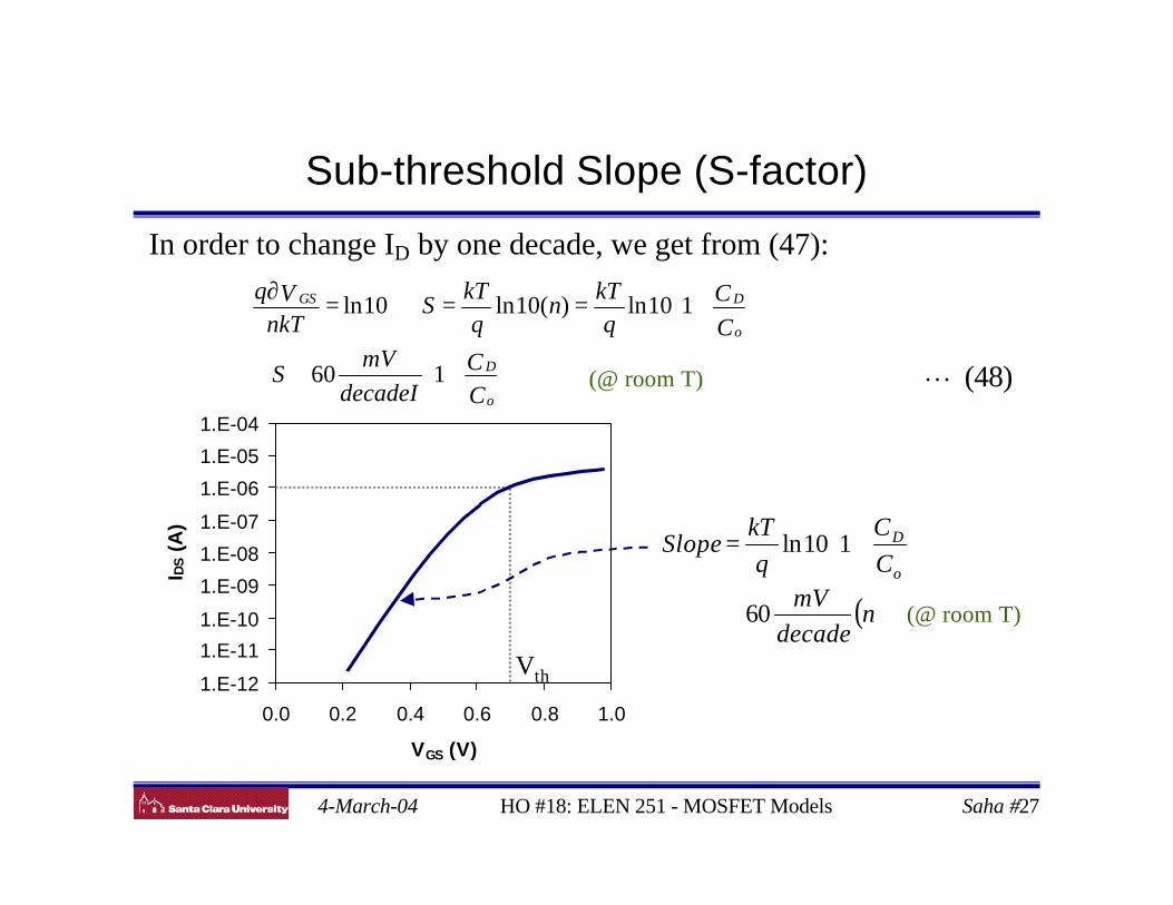
Sub-threshold Slope (S-factor)
1.E-12
1.E-11
1.E-10
1.E-09
1.E-08
1.E-07
1.E-06
1.E-05
1.E-04
0.0 0.2 0.4 0.6 0.8 1.0
VGS (V)
I DS (
A)
( )ndecade
mVC
C
q
kTSlope
o
D
60
110ln
≅
+=
(@ room T)
Vth
In order to change ID by one decade, we get from (47):
+≅∴
+==⇒=∂
CC
decadeI
mVS
C
Cq
kTn
qkT
SnkT
Vq
o
D
o
DGS
160
110ln)(10ln10ln
(@ room T) . . . (48)
4-March-04 HO #18: ELEN 251 - MOSFET Models Saha #28
Sub-threshold Model - Final Note
• In weak inversion or subthreshold region, MOS devices haveexponential characteristics but are less “efficient” than BJTsbecause n > 1.
• Subthreshold slope S does not scale and is ≈ constant. Therefore,Vth can not be scaled as required by the ideal scaling laws.
• VDS affects Vth as well as subthreshold currents.
• In order to optimize S, the desirable parameters are:
– thin oxide
– low NA
– high VSub.

4-March-04 HO #18: ELEN 251 - MOSFET Models Saha #29
Level 2/3 MOSFET Model Current
• Using sub-threshold region model, for VG < Von, we can show:
Here Von = VG at the point of intersection between the strong andweak inversion while Ion = ID @ VG = Von
• Thus, the complete long-channel DC MOSFET model is given by:
(50)
( )
( ) ( ).12
]2
[
exp
2DthG
DD
thG
onGon
VVV
VV
VV
nkT
VVqI
λαβ
αβ
+−
−−
−
VG ≤ Von (cut-off region)
VG ≥ Vth, VD ≤ VDSAT (linear region)
VG ≥ Vth, VD ≥ VDSAT (saturation region)
=DI
(49)( )
nkTVVq
onD
onG
eII−
=
4-March-04 HO #18: ELEN 251 - MOSFET Models Saha #30
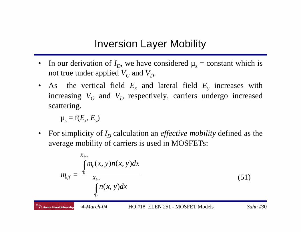
Inversion Layer Mobility
• In our derivation of ID, we have considered µs = constant which isnot true under applied VG and VD.
• As the vertical field Ex and lateral field Ey increases withincreasing VG and VD respectively, carriers undergo increasedscattering.
∴ µs = f(Ex, Ey)
• For simplicity of ID calculation an effective mobility defined as theaverage mobility of carriers is used in MOSFETs:
(51)
∫
∫=
inv
inv
X
X
s
eff
dxyxn
dxyxnyx
0
0
),(
),(),(µµ
4-March-04 HO #18: ELEN 251 - MOSFET Models Saha #31
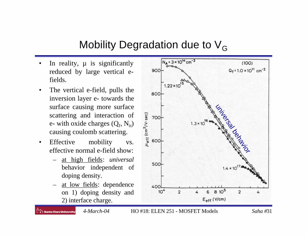
Mobility Degradation due to VG
• In reality, µ is significantlyreduced by large vertical e-fields.
• The vertical e-field, pulls theinversion layer e- towards thesurface causing more surfacescattering and interaction ofe- with oxide charges (Qf, Nit)causing coulomb scattering.
• Effective mobility vs.effective normal e-field show:
– at high fields: universalbehavior independent ofdoping density.
– at low fields: dependenceon 1) doping density and2) interface charge.
universal behavior

4-March-04 HO #18: ELEN 251 - MOSFET Models Saha #32
Mobility Degradation due to VG
• Mobility versus effective normal electric field curve is modeledusing three components:
– coulomb scattering (due to ionized impurity)
– phonon scattering - almost constant
– surface roughness scattering (at Si/SiO2 interface).
• At low normal fields:
– less inversion charge density
– ionized impurity scattering dominates and µeff = f(NA).
• At high normal fields:
– higher inversion charge density close to the interface
– surface roughness scattering dominates.
4-March-04 HO #18: ELEN 251 - MOSFET Models Saha #33
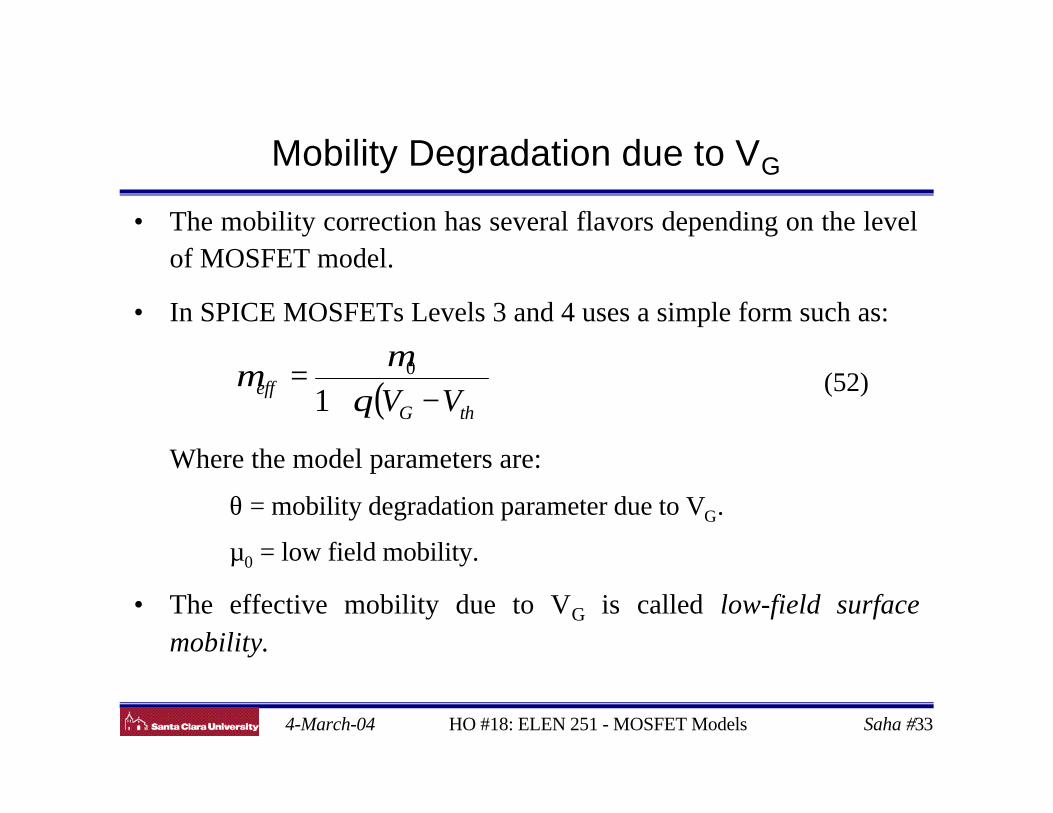
Mobility Degradation due to VG
• The mobility correction has several flavors depending on the levelof MOSFET model.
• In SPICE MOSFETs Levels 3 and 4 uses a simple form such as:
Where the model parameters are:
θ = mobility degradation parameter due to VG.
µ0 = low field mobility.
• The effective mobility due to VG is called low-field surfacemobility.
( )thGeff VV −+
=θ
µµ
10
(52)
4-March-04 HO #18: ELEN 251 - MOSFET Models Saha #34
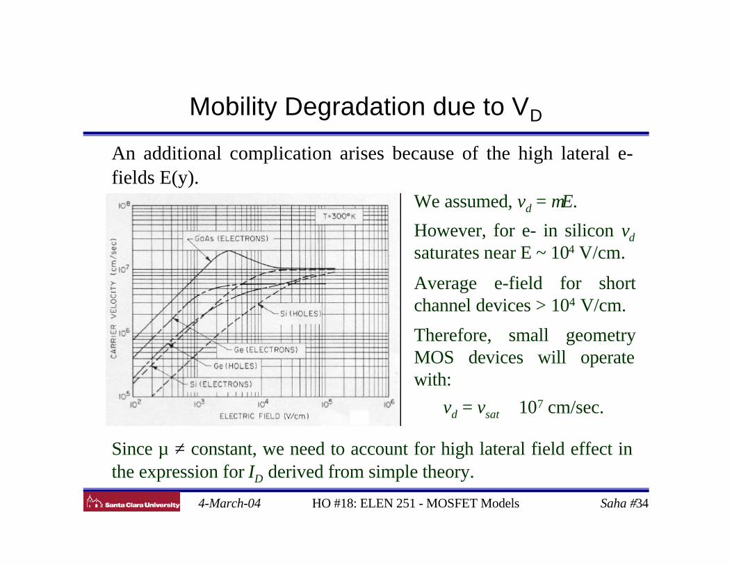
Mobility Degradation due to VD
We assumed, vd = µE.
However, for e- in silicon vd
saturates near E ~ 104 V/cm.
Average e-field for shortchannel devices > 104 V/cm.
Therefore, small geometryMOS devices will operatewith:
vd = vsat ≅ 107 cm/sec.
An additional complication arises because of the high lateral e-fields E(y).
Since µ ≠ constant, we need to account for high lateral field effect inthe expression for ID derived from simple theory.
4-March-04 HO #18: ELEN 251 - MOSFET Models Saha #35
Mobility Degradation due to VD
• The velocity saturation of inversion carriers due to increasedlateral field causes:
– current saturation sooner than predicted by VDSAT = VG – Vth
– lower IDSAT than the predicted value by simple theory.
• The drift velocity due to high field effect is given by:
• Where EC ≡ vsat/µs = critical lateral field for velocity saturation.
• For simplicity of numerical solution, β = 1 is used for modeling.
( )[ ] ββ
µ1
1 Cy
ys
EE
Ev
+=
satv
yE
s
Ev ys
µ
µ
+=∴
1 (53)
4-March-04 HO #18: ELEN 251 - MOSFET Models Saha #36
Modeling Mobility Degradation
• The effective mobility due to combine effect of VG and VD isgiven by:
Where θC ≡ 1/LEC
L = channel length of MOSFETs.
• Thus, µeff is modeled by the parameter set:
– {(µ0, θ, θb, and vsat (EC)}.
• The model parameters are obtained by curve fitting theexperimental data to the model equation.
( ) DcBbthGeff VVVV θθθ
µµ
++−+=
10
(54)
4-March-04 HO #18: ELEN 251 - MOSFET Models Saha #37
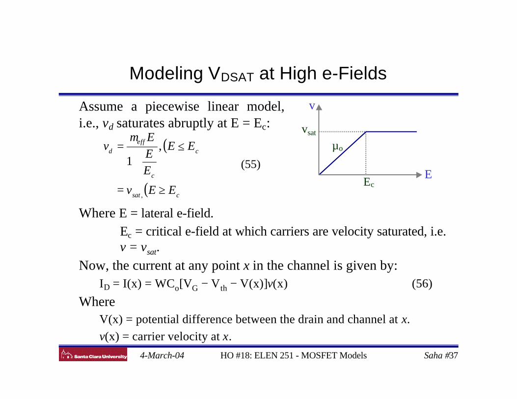
Modeling VDSAT at High e-Fields
Where E = lateral e-field. Ec = critical e-field at which carriers are velocity saturated, i.e.
v = vsat.
Now, the current at any point x in the channel is given by: ID = I(x) = WCo[VG − Vth − V(x)]v(x) (56)
Where V(x) = potential difference between the drain and channel at x.
v(x) = carrier velocity at x.
Assume a piecewise linear model,i.e., vd saturates abruptly at E = Ec: vsat
v
EcE
µo( )
( )csat
c
c
effd
EEv
EE
EEE
v
≥=
≤+
=
,
,1
µ
(55)
4-March-04 HO #18: ELEN 251 - MOSFET Models Saha #38
Modeling VDSAT at High e-Fields
Substituting (55) in (56) we get:
Integrating (57) from x = 0 to x = L and V(x) = 0 to V(x) = VD, we getin the linear region (VDS ≤ VDSAT):
Let us define, VDSAT = the drain saturation voltage due to vsat. i.e. at E = Ec.
Using this condition in (57) we get in the saturation region (VDS ≥ VDSAT):
[ ] dxxdV
EIxVVVCW
IxE
c
DthGoeff
D )(
)()( =
−−−=
µ (57)
+
−−
=
LEV
L
VVVVCWI
c
DS
DSDSthGoeff
D
1
21
µ
(58)
( )2
cDSATthGoeffD
EVVVCWI
−−=
µ(59)
4-March-04 HO #18: ELEN 251 - MOSFET Models Saha #39
Modeling VDSAT at High e-Fields
ID given by (58) and (59) must be continuous @ VDS = VDSAT.Thus, Equating (58) and (59) we can solve for VDSAT:
From (60), if L is large, VDSAT → (VG − Vth) used in the simpletheory.
Eq (60) is used to calculate drain current ID for VD > VDSAT inBSIM3 and BSIM4 MOSFET models.
(60)
( )( )
LEVV
VV
VVLE
VVLEV
C
thG
thG
thGC
thGCDSAT −
+
−=
−+−
=1
4-March-04 HO #18: ELEN 251 - MOSFET Models Saha #40
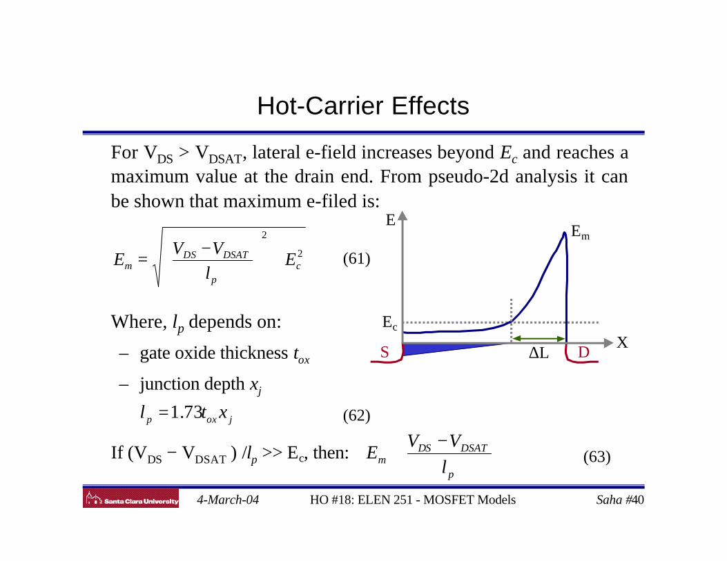
Hot-Carrier Effects
For VDS > VDSAT, lateral e-field increases beyond Ec and reaches amaximum value at the drain end. From pseudo-2d analysis it canbe shown that maximum e-filed is:
Where, lp depends on:
– gate oxide thickness tox
– junction depth xj
If (VDS − VDSAT ) /lp >> Ec, then:
DSX
EEm
Ec
∆L
2
2
cp
DSATDSm E
l
VVE +
−= (61)
joxp xtl 73.1= (62)
p
DSATDSm l
VVE
−≅ (63)
4-March-04 HO #18: ELEN 251 - MOSFET Models Saha #41
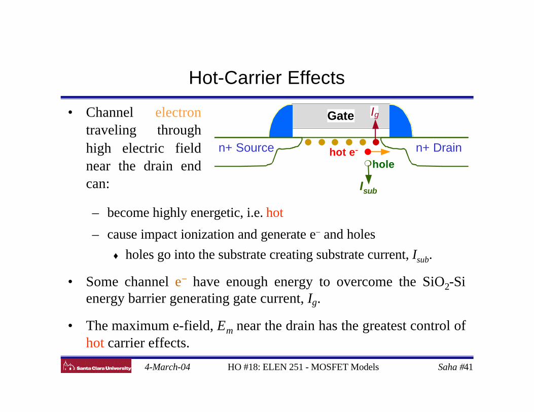
Hot-Carrier Effects
• Channel electrontraveling throughhigh electric fieldnear the drain endcan:
– become highly energetic, i.e. hot
– cause impact ionization and generate e− and holes
♦ holes go into the substrate creating substrate current, Isub.
• Some channel e− have enough energy to overcome the SiO2-Sienergy barrier generating gate current, Ig.
• The maximum e-field, Em near the drain has the greatest control ofhot carrier effects.
Gate Ig
n+ Drainn+ Source
Isub
❍holehot e−− ●
●● ● ● ● ●

4-March-04 HO #18: ELEN 251 - MOSFET Models Saha #42
Substrate Current Modeling
Impact ionization coefficient, α = Aiexp(−Bi/E). Then the substratecurrent due to impact ionization is:
Where x = o ⇒ start of impact ionization region with E = Ec. x = lp ⇒ length of impact ionization region with E = Em.
Changing the limits of integration to E in (19) and after integrationwe get:
∴ As Em↑, Isub↑.
dxeAI
dxII
xE
B
i
l
o
D
l
o
Dsub
ip
p
)(−
∫
∫
=
= α
(64)
−
=
m
iDmp
i
isub E
BIEl
B
AI exp (65)