
MOSFET - Royal Institute of Technology · MOSFET characteristics require computer models that have...
21
MOSFET 1 MOSFET Two power MOSFETs in the surface-mount package D2PAK. Operating as switches, each of these components can sustain a blocking voltage of 120 volts in the OFF state, and can conduct a continuous current of 30 amperes in the ON state, dissipating up to about 100 watts and controlling a load of over 2000 watts. A matchstick is pictured for scale. A cross section through an nMOSFET when the gate voltage V GS is below the threshold for making a conductive channel; there is little or no conduction between the terminals source and drain; the switch is off. When the gate is more positive, it attracts electrons, inducing an n-type conductive channel in the substrate below the oxide, which allows electrons to flow between the n-doped terminals; the switch is on. The metal–oxide–semiconductor field-effect transistor (MOSFET, MOS-FET, or MOS FET) is a device used for amplifying or switching electronic signals. The basic principle of the device was first proposed by Julius Edgar Lilienfeld in 1925. In MOSFETs, a voltage on the oxide-insulated gate electrode can induce a conducting channel between the two other contacts called source and drain. The channel can be of n-type or p-type (see article on semiconductor devices), and is accordingly called an nMOSFET or a pMOSFET (also commonly nMOS, pMOS). It is by far the most common transistor in both digital and analog circuits, though the bipolar junction transistor was at one time much more common. The 'metal' in the name is now often a misnomer because the previously metal gate material is now often a layer of polysilicon (polycrystalline silicon). Aluminium had been the gate material until the mid 1970s, when polysilicon became dominant, due to its capability to form self-aligned gates. Metallic gates are regaining popularity, since it is difficult to increase the speed of operation of transistors without metal gates. IGFET is a related term meaning insulated-gate field-effect transistor, and is almost synonymous with MOSFET, though it can refer to FETs with a gate insulator that is not oxide. Another synonym is MISFET for metal–insulator–semiconductor FET.
Transcript of MOSFET - Royal Institute of Technology · MOSFET characteristics require computer models that have...
MOSFET 1
MOSFET
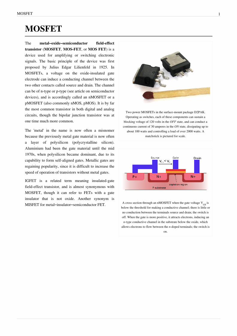
Two power MOSFETs in the surface-mount package D2PAK.Operating as switches, each of these components can sustain a
blocking voltage of 120 volts in the OFF state, and can conduct acontinuous current of 30 amperes in the ON state, dissipating up to
about 100 watts and controlling a load of over 2000 watts. Amatchstick is pictured for scale.
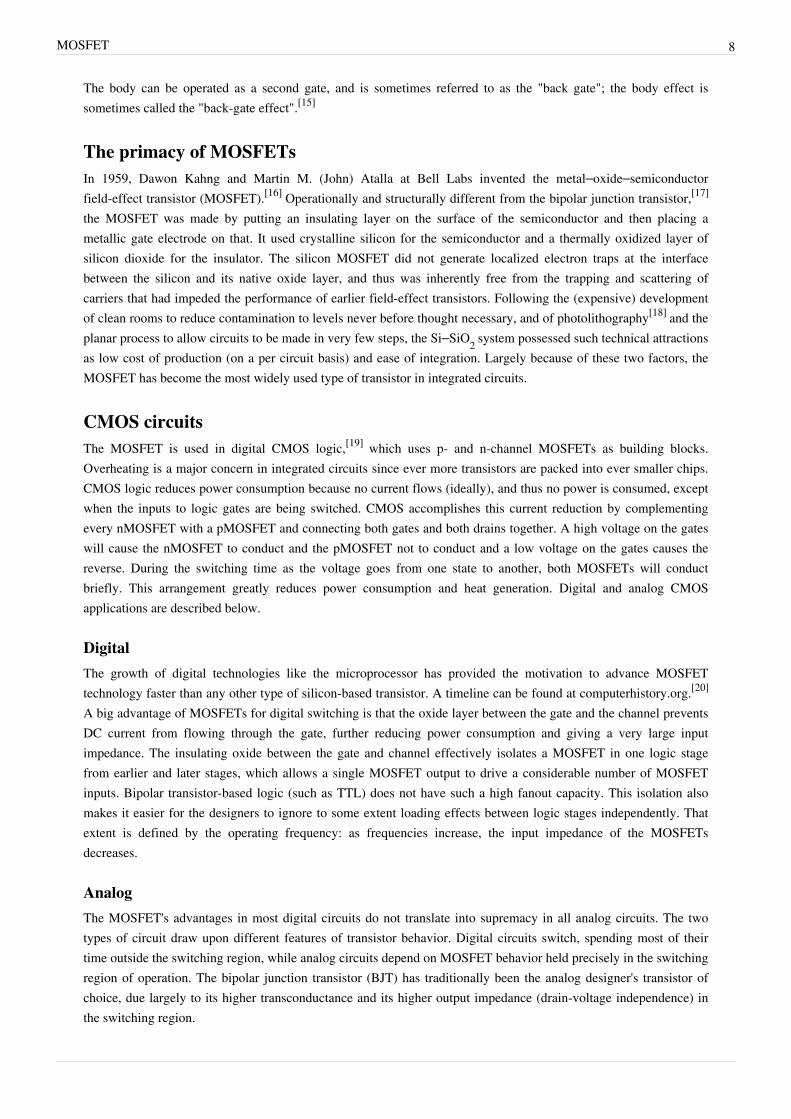
A cross section through an nMOSFET when the gate voltage VGS isbelow the threshold for making a conductive channel; there is little orno conduction between the terminals source and drain; the switch isoff. When the gate is more positive, it attracts electrons, inducing ann-type conductive channel in the substrate below the oxide, which
allows electrons to flow between the n-doped terminals; the switch ison.
The metal–oxide–semiconductor field-effecttransistor (MOSFET, MOS-FET, or MOS FET) is adevice used for amplifying or switching electronicsignals. The basic principle of the device was firstproposed by Julius Edgar Lilienfeld in 1925. InMOSFETs, a voltage on the oxide-insulated gateelectrode can induce a conducting channel between thetwo other contacts called source and drain. The channelcan be of n-type or p-type (see article on semiconductordevices), and is accordingly called an nMOSFET or apMOSFET (also commonly nMOS, pMOS). It is by farthe most common transistor in both digital and analogcircuits, though the bipolar junction transistor was atone time much more common.
The 'metal' in the name is now often a misnomerbecause the previously metal gate material is now oftena layer of polysilicon (polycrystalline silicon).Aluminium had been the gate material until the mid1970s, when polysilicon became dominant, due to itscapability to form self-aligned gates. Metallic gates areregaining popularity, since it is difficult to increase thespeed of operation of transistors without metal gates.
IGFET is a related term meaning insulated-gatefield-effect transistor, and is almost synonymous withMOSFET, though it can refer to FETs with a gateinsulator that is not oxide. Another synonym isMISFET for metal–insulator–semiconductor FET.

MOSFET 2
Simulation result for formation of inversion channel (electron density) and attainment ofthreshold voltage (IV) in a nanowire MOSFET. Note that the threshold voltage for this
device lies around 0.45V.
Composition
Photomicrograph of two metal-gate MOSFETs in a test pattern. Probe pads for twogates and three source/drain nodes are labeled.
Usually the semiconductor of choice issilicon, but some chip manufacturers, mostnotably IBM, recently started using achemical compound of silicon andgermanium (SiGe) in MOSFET channels.Unfortunately, many semiconductors withbetter electrical properties than silicon, suchas gallium arsenide, do not form goodsemiconductor-to-insulator interfaces, thusare not suitable for MOSFETs. Researchcontinues on creating insulators withacceptable electrical characteristics on othersemiconductor material.
In order to overcome power consumptionincrease due to gate current leakage, high-κdielectric replaces silicon dioxide for the gate insulator, while metal gates return by replacing polysilicon (see Intelannouncement[1] ).
The gate is separated from the channel by a thin insulating layer, traditionally of silicon dioxide and later of siliconoxynitride. Some companies have started to introduce a high-κ dielectric + metal gate combination in the 45nanometer node.When a voltage is applied between the gate and body terminals, the electric field generated penetrates through theoxide and creates an alleged "inversion layer" or "channel" at the semiconductor-insulator interface. The inversionchannel is of the same type, P-type or N-type, as the source and drain, thus it provides a channel through whichcurrent can pass. Varying the voltage between the gate and body modulates the conductivity of this layer and allowsto control the current flow between drain and source.

MOSFET 3
Circuit symbolsA variety of symbols are used for the MOSFET. The basic design is generally a line for the channel with the sourceand drain leaving it at right angles and then bending back at right angles into the same direction as the channel.Sometimes three line segments are used for enhancement mode and a solid line for depletion mode. Another line isdrawn parallel to the channel for the gate.The bulk connection, if shown, is shown connected to the back of the channel with an arrow indicating PMOS orNMOS. Arrows always point from P to N, so an NMOS (N-channel in P-well or P-substrate) has the arrow pointingin (from the bulk to the channel). If the bulk is connected to the source (as is generally the case with discrete devices)it is sometimes angled to meet up with the source leaving the transistor. If the bulk is not shown (as is often the casein IC design as they are generally common bulk) an inversion symbol is sometimes used to indicate PMOS,alternatively an arrow on the source may be used in the same way as for bipolar transistors (out for nMOS, in forpMOS).Comparison of enhancement-mode and depletion-mode MOSFET symbols, along with JFET symbols (drawn withsource and drain ordered such that higher voltages appear higher on the page than lower voltages):
P-channel
N-channel
JFET MOSFET enh MOSFET enh (no bulk) MOSFET dep
For the symbols in which the bulk, or body, terminal is shown, it is here shown internally connected to the source.This is a typical configuration, but by no means the only important configuration. In general, the MOSFET is afour-terminal device, and in integrated circuits many of the MOSFETs share a body connection, not necessarilyconnected to the source terminals of all the transistors.
MOSFET operation
Example application of an N-Channel MOSFET.When the switch is pushed the LED lights up.[2]
Metal–oxide–semiconductor structure
A traditional metal–oxide–semiconductor (MOS) structure is obtainedby growing a layer of silicon dioxide (SiO2) on top of a siliconsubstrate and depositing a layer of metal or polycrystalline silicon (thelatter is commonly used). As the silicon dioxide is a dielectric material,its structure is equivalent to a planar capacitor, with one of theelectrodes replaced by a semiconductor.
When a voltage is applied across a MOS structure, it modifies thedistribution of charges in the semiconductor. If we consider a P-typesemiconductor (with the density of acceptors, p the density of holes; p= NA in neutral bulk), a positive voltage, , from gate to body (seefigure) creates a depletion layer by forcing the positively charged holesaway from the gate-insulator/semiconductor interface,

MOSFET 4
Metal–oxide–semiconductor structure on P-typesilicon
leaving exposed a carrier-free region of immobile, negatively chargedacceptor ions (see doping (semiconductor)). If is high enough, a highconcentration of negative charge carriers forms in an inversion layerlocated in a thin layer next to the interface between the semiconductorand the insulator. Unlike the MOSFET, where the inversion layerelectrons are supplied rapidly from the source/drain electrodes, in theMOS capacitor they are produced much more slowly by thermalgeneration through carrier generation and recombination centers in thedepletion region. Conventionally, the gate voltage at which the volume density of electrons in the inversion layer isthe same as the volume density of holes in the body is called the threshold voltage.
This structure with P-type body is the basis of the N-type MOSFET, which requires the addition of an N-type sourceand drain regions.
MOSFET structure and channel formation
Cross section of an NMOS without channelformed: OFF state
Cross section of an NMOS with channel formed:ON state
A metal–oxide–semiconductor field-effect transistor (MOSFET) isbased on the modulation of charge concentration by a MOScapacitance between a body electrode and a gate electrode locatedabove the body and insulated from all other device regions by a gatedielectric layer which in the case of a MOSFET is an oxide, such assilicon dioxide. If dielectrics other than an oxide such as silicondioxide (often referred to as oxide) are employed the device may bereferred to as a metal–insulator–semiconductor FET (MISFET).Compared to the MOS capacitor, the MOSFET includes two additionalterminals (source and drain), each connected to individual highlydoped regions that are separated by the body region. These regions canbe either p or n type, but they must both be of the same type, and ofopposite type to the body region. The source and drain (unlike thebody) are highly doped as signified by a '+' sign after the type ofdoping.
If the MOSFET is an n-channel or nMOS FET, then the source anddrain are 'n+' regions and the body is a 'p' region. As described above,with sufficient gate voltage, holes from the body are driven away fromthe gate, forming an inversion layer or n-channel at the interfacebetween the p region and the oxide. This conducting channel extendsbetween the source and the drain, and current is conducted through itwhen a voltage is applied between source and drain.
For gate voltages below the threshold value, the channel is lightlypopulated, and only a very small subthreshold leakage current can flowbetween the source and the drain.
If the MOSFET is a p-channel or pMOS FET, then the source and drain are 'p+' regions and the body is a 'n' region.When a negative gate-source voltage (positive source-gate) is applied, it creates a p-channel at the surface of the nregion, analogous to the n-channel case, but with opposite polarities of charges and voltages. When a voltage lessnegative than the threshold value (a negative voltage for p-channel) is applied between gate and source, the channeldisappears and only a very small subthreshold current can flow between the source and the drain.

MOSFET 5
The source is so named because it is the source of the charge carriers (electrons for n-channel, holes for p-channel)that flow through the channel; similarly, the drain is where the charge carriers leave the channel.The device may comprise a Silicon On Insulator (SOI) device in which a Buried OXide (BOX) is formed below athin semiconductor layer. If the channel region between the gate dielectric and a Buried Oxide (BOX) region is verythin, the very thin channel region is referred to as an Ultra Thin Channel (UTC) region with the source and drainregions formed on either side thereof in and/or above the thin semiconductor layer. Alternatively, the device maycomprise a SEMiconductor On Insulator (SEMOI) device in which semiconductors other than silicon are employed.Many alternative semicondutor materials may be employed.When the source and drain regions are formed above the channel in whole or in part, they are referred to as RaisedSource/Drain (RSD) regions.
Modes of operationThe operation of a MOSFET can be separated into three different modes, depending on the voltages at the terminals.In the following discussion, a simplified algebraic model is used that is accurate only for old technology. ModernMOSFET characteristics require computer models that have rather more complex behavior.For an enhancement-mode, n-channel MOSFET, the three operational modes are:Cutoff, subthreshold, or weak-inversion mode
When VGS
< Vth
:
where is the threshold voltage of the device.According to the basic threshold model, the transistor is turned off, and there is no conduction between drainand source. In reality, the Boltzmann distribution of electron energies allows some of the more energeticelectrons at the source to enter the channel and flow to the drain, resulting in a subthreshold current that is anexponential function of gate–source voltage. While the current between drain and source should ideally bezero when the transistor is being used as a turned-off switch, there is a weak-inversion current, sometimescalled subthreshold leakage.In weak inversion the current varies exponentially with gate-to-source bias as given approximately by:[3]
[4]
,
where = current at and the slope factor n is given by
,with = capacitance of the depletion layer and = capacitance of the oxide layer. In a long-channeldevice, there is no drain voltage dependence of the current once , but as channel length isreduced drain-induced barrier lowering introduces drain voltage dependence that depends in a complex wayupon the device geometry (for example, the channel doping, the junction doping and so on). Frequently,threshold voltage Vth for this mode is defined as the gate voltage at which a selected value of current ID0occurs, for example, ID0 = 1 μA, which may not be the same Vth-value used in the equations for the followingmodes.Some micropower analog circuits are designed to take advantage of subthreshold conduction.[5] [6] [7] Byworking in the weak-inversion region, the MOSFETs in these circuits deliver the highest possibletransconductance-to-current ratio, namely: , almost that of a bipolar transistor.[8]
The subthreshold I–V curve depends exponentially upon threshold voltage, introducing a strong dependenceon any manufacturing variation that affects threshold voltage; for example: variations in oxide thickness,junction depth, or body doping that change the degree of drain-induced barrier lowering. The resultingsensitivity to fabricational variations complicates optimization for leakage and performance.[9] [10]

MOSFET 6
MOSFET drain current vs. drain-to-source voltage for several values of; the boundary between linear (Ohmic) and saturation (active)
modes is indicated by the upward curving parabola.
Cross section of a MOSFET operating in thelinear (Ohmic) region; strong inversion region
present even near drain
Cross section of a MOSFET operating in thesaturation (active) region; channel exhibits
pinch-off near drain
Triode mode or linear region (also known asthe ohmic mode[11] [12] )
When VGS
> Vth
and VDS
< ( VGS
-V
th )
The transistor is turned on, and achannel has been created whichallows current to flow between thedrain and the source. The MOSFEToperates like a resistor, controlled bythe gate voltage relative to both thesource and drain voltages. The currentfrom drain to source is modeled as:
where is the charge-carrier effective mobility, is the gate width, is the gate length and is thegate oxide capacitance per unit area. The transition from the exponential subthreshold region to the trioderegion is not as sharp as the equations suggest.
Saturation or active mode[3] [13]
When VGS
> Vth
and VDS
> ( VGS
- Vth
)
The switch is turned on, and a channel has been created, which allows current to flow between the drain and source. Since the drain voltage is higher than the gate voltage, the electrons spread out, and conduction is not

MOSFET 7
through a narrow channel but through a broader, two- or three-dimensional current distribution extendingaway from the interface and deeper in the substrate. The onset of this region is also known as pinch-off toindicate the lack of channel region near the drain. The drain current is now weakly dependent upon drainvoltage and controlled primarily by the gate–source voltage, and modeled very approximately as:
The additional factor involving λ, the channel-length modulation parameter, models current dependence ondrain voltage due to the Early effect, or channel length modulation. According to this equation, a key designparameter, the MOSFET transconductance is:
,where the combination Vov = VGS - Vth is called the overdrive voltage.[14] Another key design parameter is theMOSFET output resistance given by:
.
rout is the inverse of gds where . VDS is the expression in saturation region.
If λ is taken as zero, an infinite output resistance of the device results that leads to unrealistic circuitpredictions, particularly in analog circuits.As the channel length becomes very short, these equations become quite inaccurate. New physical effectsarise. For example, carrier transport in the active mode may become limited by velocity saturation. Whenvelocity saturation dominates, the saturation drain current is more nearly linear than quadratic in VGS. At evenshorter lengths, carriers transport with near zero scattering, known as quasi-ballistic transport. In addition, theoutput current is affected by drain-induced barrier lowering of the threshold voltage.
Body effect
Ohmic contact to body to ensure no body bias; top left:subthreshold, top right:Ohmicmode, bottom left:Active mode at onset of pinch-off, bottom right: Active mode well into
pinch-off - channel length modulation evident
The body effect describes the changesin the threshold voltage by the changein the source-bulk voltage,approximated by the followingequation:
,
where is the threshold voltage with substrate bias present, and is the zero- value of thresholdvoltage, is the body effect parameter, and is the surface potential parameter.
MOSFET 8
The body can be operated as a second gate, and is sometimes referred to as the "back gate"; the body effect issometimes called the "back-gate effect".[15]
The primacy of MOSFETsIn 1959, Dawon Kahng and Martin M. (John) Atalla at Bell Labs invented the metal–oxide–semiconductorfield-effect transistor (MOSFET).[16] Operationally and structurally different from the bipolar junction transistor,[17]
the MOSFET was made by putting an insulating layer on the surface of the semiconductor and then placing ametallic gate electrode on that. It used crystalline silicon for the semiconductor and a thermally oxidized layer ofsilicon dioxide for the insulator. The silicon MOSFET did not generate localized electron traps at the interfacebetween the silicon and its native oxide layer, and thus was inherently free from the trapping and scattering ofcarriers that had impeded the performance of earlier field-effect transistors. Following the (expensive) developmentof clean rooms to reduce contamination to levels never before thought necessary, and of photolithography[18] and theplanar process to allow circuits to be made in very few steps, the Si–SiO2 system possessed such technical attractionsas low cost of production (on a per circuit basis) and ease of integration. Largely because of these two factors, theMOSFET has become the most widely used type of transistor in integrated circuits.
CMOS circuitsThe MOSFET is used in digital CMOS logic,[19] which uses p- and n-channel MOSFETs as building blocks.Overheating is a major concern in integrated circuits since ever more transistors are packed into ever smaller chips.CMOS logic reduces power consumption because no current flows (ideally), and thus no power is consumed, exceptwhen the inputs to logic gates are being switched. CMOS accomplishes this current reduction by complementingevery nMOSFET with a pMOSFET and connecting both gates and both drains together. A high voltage on the gateswill cause the nMOSFET to conduct and the pMOSFET not to conduct and a low voltage on the gates causes thereverse. During the switching time as the voltage goes from one state to another, both MOSFETs will conductbriefly. This arrangement greatly reduces power consumption and heat generation. Digital and analog CMOSapplications are described below.
DigitalThe growth of digital technologies like the microprocessor has provided the motivation to advance MOSFETtechnology faster than any other type of silicon-based transistor. A timeline can be found at computerhistory.org.[20]
A big advantage of MOSFETs for digital switching is that the oxide layer between the gate and the channel preventsDC current from flowing through the gate, further reducing power consumption and giving a very large inputimpedance. The insulating oxide between the gate and channel effectively isolates a MOSFET in one logic stagefrom earlier and later stages, which allows a single MOSFET output to drive a considerable number of MOSFETinputs. Bipolar transistor-based logic (such as TTL) does not have such a high fanout capacity. This isolation alsomakes it easier for the designers to ignore to some extent loading effects between logic stages independently. Thatextent is defined by the operating frequency: as frequencies increase, the input impedance of the MOSFETsdecreases.
AnalogThe MOSFET's advantages in most digital circuits do not translate into supremacy in all analog circuits. The twotypes of circuit draw upon different features of transistor behavior. Digital circuits switch, spending most of theirtime outside the switching region, while analog circuits depend on MOSFET behavior held precisely in the switchingregion of operation. The bipolar junction transistor (BJT) has traditionally been the analog designer's transistor ofchoice, due largely to its higher transconductance and its higher output impedance (drain-voltage independence) inthe switching region.

MOSFET 9
Nevertheless, MOSFETs are widely used in many types of analog circuits because of certain advantages. Thecharacteristics and performance of many analog circuits can be designed by changing the sizes (length and width) ofthe MOSFETs used. By comparison, in most bipolar transistors the size of the device does not significantly affect theperformance. MOSFETs' ideal characteristics regarding gate current (zero) and drain-source offset voltage (zero)also make them nearly ideal switch elements, and also make switched capacitor analog circuits practical. In theirlinear region, MOSFETs can be used as precision resistors, which can have a much higher controlled resistance thanBJTs. In high power circuits, MOSFETs sometimes have the advantage of not suffering from thermal runaway asBJTs do. Also, they can be formed into capacitors and gyrator circuits which allow op-amps made from them toappear as inductors, thereby allowing all of the normal analog devices, except for diodes (which can be made smallerthan a MOSFET anyway), to be built entirely out of MOSFETs. This allows for complete analog circuits to be madeon a silicon chip in a much smaller space.Some ICs combine analog and digital MOSFET circuitry on a single mixed-signal integrated circuit, making theneeded board space even smaller. This creates a need to isolate the analog circuits from the digital circuits on a chiplevel, leading to the use of isolation rings and Silicon-On-Insulator (SOI). The main advantage of BJTs versusMOSFETs in the analog design process is the ability of BJTs to handle a larger current in a smaller space.Fabrication processes exist that incorporate BJTs and MOSFETs into a single device. Mixed-transistor devices arecalled Bi-FETs (Bipolar-FETs) if they contain just one BJT-FET and BiCMOS (bipolar-CMOS) if they containcomplementary BJT-FETs. Such devices have the advantages of both insulated gates and higher current density.BJTs have some advantages over MOSFETs for at least two digital applications. Firstly, in high speed switching,they do not have the "larger" capacitance from the gate, which when multiplied by the resistance of the channel givesthe intrinsic time constant of the process. The intrinsic time constant places a limit on the speed a MOSFET canoperate at because higher frequency signals are filtered out. Widening the channel reduces the resistance of thechannel, but increases the capacitance by the exact same amount. Reducing the width of the channel increases theresistance, but reduces the capacitance by the same amount. R*C=Tc1, 0.5R*2C=Tc1, 2R*0.5C=Tc1. There is noway to minimize the intrinsic time constant for a certain process. Different processes using different channel lengths,channel heights, gate thicknesses and materials will have different intrinsic time constants. This problem is mostlyavoided with a BJT because it does not have a gate.The second application where BJTs have an advantage over MOSFETs stems from the first. When driving manyother gates, called fanout, the resistance of the MOSFET is in series with the gate capacitances of the other FETs,creating a secondary time constant. Delay circuits use this fact to create a fixed signal delay by using a small CMOSdevice to send a signal to many other, many times larger CMOS devices. The secondary time constant can beminimized by increasing the driving FET's channel width to decrease its resistance and decreasing the channelwidths of the FETs being driven, decreasing their capacitance. The drawback is that it increases the capacitance ofthe driving FET and increases the resistance of the FETs being driven, but usually these drawbacks are a minimalproblem when compared to the timing problem. BJTs are better able to drive the other gates because they can outputmore current than MOSFETs, allowing for the FETs being driven to charge faster. Many chips use MOSFET inputsand BiCMOS outputs (see above).
MOSFET scalingOver the past decades, the MOSFET has continually been scaled down in size; typical MOSFET channel lengths were once several micrometres, but modern integrated circuits are incorporating MOSFETs with channel lengths of tens of nanometers. Intel began production of a process featuring a 32 nm feature size (with the channel being even shorter) in late 2009. The semiconductor industry maintains a "roadmap", the ITRS [21] , which sets the pace for MOSFET development. Historically, the difficulties with decreasing the size of the MOSFET have been associated with the semiconductor device fabrication process, the need to use very low voltages, and with poorer electrical performance necessitating circuit redesign and innovation (small MOSFETs exhibit higher leakage currents, and

MOSFET 10
lower output resistance, discussed below).
Reasons for MOSFET scalingSmaller MOSFETs are desirable for several reasons. The main reason to make transistors smaller is to pack moreand more devices in a given chip area. This results in a chip with the same functionality in a smaller area, or chipswith more functionality in the same area. Since fabrication costs for a semiconductor wafer are relatively fixed, thecost per integrated circuits is mainly related to the number of chips that can be produced per wafer. Hence, smallerICs allow more chips per wafer, reducing the price per chip. In fact, over the past 30 years the number of transistorsper chip has been doubled every 2–3 years once a new technology node is introduced. For example the number ofMOSFETs in a microprocessor fabricated in a 45 nm technology is twice as many as in a 65 nm chip. This doublingof the transistor count was first observed by Gordon Moore in 1965 and is commonly referred to as Moore's law.[22]
Trend of Intel CPU transistor gate length
It is also expected that smallertransistors switch faster. For example,one approach to size reduction is ascaling of the MOSFET that requiresall device dimensions to reduceproportionally. The main devicedimensions are the transistor length,width, and the oxide thickness, each(used to) scale with a factor of 0.7 pernode. This way, the transistor channelresistance does not change withscaling, while gate capacitance is cutby a factor of 0.7. Hence, the RC delayof the transistor scales with a factor of0.7.
While this has been traditionally the case for the older technologies, for the state-of-the-art MOSFETs reduction ofthe transistor dimensions does not necessarily translate to higher chip speed because the delay due tointerconnections is more significant.
Difficulties arising due to MOSFET size reductionProducing MOSFETs with channel lengths much smaller than a micrometer is a challenge, and the difficulties ofsemiconductor device fabrication are always a limiting factor in advancing integrated circuit technology. In recentyears, the small size of the MOSFET, below a few tens of nanometers, has created operational problems.
Higher subthreshold conduction
As MOSFET geometries shrink, the voltage that can be applied to the gate must be reduced to maintain reliability.To maintain performance, the threshold voltage of the MOSFET has to be reduced as well. As threshold voltage isreduced, the transistor cannot be switched from complete turn-off to complete turn-on with the limited voltage swingavailable; the circuit design is a compromise between strong current in the "on" case and low current in the "off"case, and the application determines whether to favor one over the other. Subthreshold leakage (includingsubthreshold conduction, gate-oxide leakage and reverse-biased junction leakage), which was ignored in the past,now can consume upwards of half of the total power consumption of modern high-performance VLSI chips.[23] [24]
[25]

MOSFET 11
Increased gate-oxide leakage
The gate oxide, which serves as insulator between the gate and channel, should be made as thin as possible toincrease the channel conductivity and performance when the transistor is on and to reduce subthreshold leakagewhen the transistor is off. However, with current gate oxides with a thickness of around 1.2 nm (which in silicon is~5 atoms thick) the quantum mechanical phenomenon of electron tunneling occurs between the gate and channel,leading to increased power consumption.Insulators (referred to as high-k dielectrics) that have a larger dielectric constant than silicon dioxide, such as groupIVb metal silicates e.g. hafnium and zirconium silicates and oxides are being used to reduce the gate leakage fromthe 45 nanometer technology node onwards. Increasing the dielectric constant of the gate dielectric allows a thickerlayer while maintaining a high capacitance (capacitance is proportional to dielectric constant and inverselyproportional to dielectric thickness). All else equal, a higher dielectric thickness reduces the quantum tunnelingcurrent through the dielectric between the gate and the channel. On the other hand, the barrier height of the new gateinsulator is an important consideration; the difference in conduction band energy between the semiconductor and thedielectric (and the corresponding difference in valence band energy) also affects leakage current level. For thetraditional gate oxide, silicon dioxide, the former barrier is approximately 8 eV. For many alternative dielectrics thevalue is significantly lower, tending to increase the tunneling current, somewhat negating the advantage of higherdielectric constant.
Increased junction leakage
To make devices smaller, junction design has become more complex, leading to higher doping levels, shallowerjunctions, "halo" doping and so forth,[26] [27] all to decrease drain-induced barrier lowering (see the section onjunction design). To keep these complex junctions in place, the annealing steps formerly used to remove damage andelectrically active defects must be curtailed[28] increasing junction leakage. Heavier doping is also associated withthinner depletion layers and more recombination centers that result in increased leakage current, even without latticedamage.
MOSFET version of gain-boosted current mirror; M1 and M2 are in active mode,while M3 and M4 are in Ohmic mode, and act like resistors. The operational
amplifier provides feedback that maintains a high output resistance
Lower output resistance
For analog operation, good gain requires ahigh MOSFET output impedance, which isto say, the MOSFET current should varyonly slightly with the applieddrain-to-source voltage. As devices aremade smaller, the influence of the draincompetes more successfully with that of thegate due to the growing proximity of thesetwo electrodes, increasing the sensitivity ofthe MOSFET current to the drain voltage.To counteract the resulting decrease inoutput resistance, circuits are made morecomplex, either by requiring more devices,for example the cascode and cascadeamplifiers, or by feedback circuitry using operational amplifiers, for example a circuit like that in the adjacent figure.
Lower transconductance
The transconductance of the MOSFET decides its gain and is proportional to hole or electron mobility (depending on device type), at least for low drain voltages. As MOSFET size is reduced, the fields in the channel increase and the

MOSFET 12
dopant impurity levels increase. Both changes reduce the carrier mobility, and hence the transconductance. Aschannel lengths are reduced without proportional reduction in drain voltage, raising the electric field in the channel,the result is velocity saturation of the carriers, limiting the current and the transconductance.
Interconnect capacitance
Traditionally, switching time was roughly proportional to the gate capacitance of gates. However, with transistorsbecoming smaller and more transistors being placed on the chip, interconnect capacitance (the capacitance of thewires connecting different parts of the chip) is becoming a large percentage of capacitance.[29] [30] Signals have totravel through the interconnect, which leads to increased delay and lower performance.
Heat production
Large heatsinks to cool power transistors in a TRM-800 audioamplifier
The ever-increasing density of MOSFETs on anintegrated circuit creates problems of substantiallocalized heat generation that can impair circuitoperation. Circuits operate slower at high temperatures,and have reduced reliability and shorter lifetimes. Heatsinks and other cooling methods are now required formany integrated circuits including microprocessors.Power MOSFETs are at risk of thermal runaway. Astheir on-state resistance rises with temperature, if theload is approximately a constant-current load then thepower loss rises correspondingly, generating furtherheat. When the heatsink is not able to keep thetemperature low enough, the junction temperature mayrise quickly and uncontrollably, resulting in destructionof the device.
In order to assist designers in the device selection process, a simulation tool such as ThermaSimTM can be used tosimulate in-circuit performance[31] .
Process variations
With MOSFETS becoming smaller, the number of atoms in the silicon that produce many of the transistor'sproperties is becoming fewer, with the result that control of dopant numbers and placement is more erratic. Duringchip manufacturing, random process variations affect all transistor dimensions: length, width, junction depths, oxidethickness etc., and become a greater percentage of overall transistor size as the transistor shrinks. The transistorcharacteristics become less certain, more statistical. The random nature of manufacture means we do not knowwhich particular example MOSFETs actually will end up in a particular instance of the circuit. This uncertaintyforces a less optimal design because the design must work for a great variety of possible component MOSFETs. Seeprocess variation, design for manufacturability, reliability engineering, and statistical process control.[32]
Modeling challenges
Modern ICs are computer-simulated with the goal of obtaining working circuits from the very first manufactured lot.As devices are miniaturized, the complexity of the processing makes it difficult to predict exactly what the finaldevices look like, and modeling of physical processes becomes more challenging as well. In addition, microscopicvariations in structure due simply to the probabilistic nature of atomic processes require statistical (not justdeterministic) predictions. These factors combine to make adequate simulation and "right the first time" manufacturedifficult.

MOSFET 13
MOSFET construction
Gate materialThe primary criterion for the gate material is that it is a good conductor. Highly-doped polycrystalline silicon is anacceptable but certainly not ideal conductor, and also suffers from some more technical deficiencies in its role as thestandard gate material. Nevertheless, there are several reasons favoring use of polysilicon:1. The threshold voltage (and consequently the drain to source on-current) is modified by the work function
difference between the gate material and channel material. Because polysilicon is a semiconductor, its workfunction can be modulated by adjusting the type and level of doping. Furthermore, because polysilicon has thesame bandgap as the underlying silicon channel, it is quite straightforward to tune the work function to achievelow threshold voltages for both NMOS and PMOS devices. By contrast, the work functions of metals are noteasily modulated, so tuning the work function to obtain low threshold voltages becomes a significant challenge.Additionally, obtaining low-threshold devices on both PMOS and NMOS devices would likely require the use ofdifferent metals for each device type, introducing additional complexity to the fabrication process.
2. The Silicon-SiO2 interface has been well studied and is known to have relatively few defects. By contrast manymetal–insulator interfaces contain significant levels of defects which can lead to Fermi-level pinning, charging, orother phenomena that ultimately degrade device performance.
3. In the MOSFET IC fabrication process, it is preferable to deposit the gate material prior to certainhigh-temperature steps in order to make better-performing transistors. Such high temperature steps would meltsome metals, limiting the types of metal that can be used in a metal-gate-based process.
While polysilicon gates have been the de facto standard for the last twenty years, they do have some disadvantageswhich have led to their likely future replacement by metal gates. These disadvantages include:1. Polysilicon is not a great conductor (approximately 1000 times more resistive than metals) which reduces the
signal propagation speed through the material. The resistivity can be lowered by increasing the level of doping,but even highly doped polysilicon is not as conductive as most metals. In order to improve conductivity further,sometimes a high-temperature metal such as tungsten, titanium, cobalt, and more recently nickel is alloyed withthe top layers of the polysilicon. Such a blended material is called silicide. The silicide-polysilicon combinationhas better electrical properties than polysilicon alone and still does not melt in subsequent processing. Also thethreshold voltage is not significantly higher than with polysilicon alone, because the silicide material is not nearthe channel. The process in which silicide is formed on both the gate electrode and the source and drain regions issometimes called salicide, self-aligned silicide.
2. When the transistors are extremely scaled down, it is necessary to make the gate dielectric layer very thin, around1 nm in state-of-the-art technologies. A phenomenon observed here is the so-called poly depletion, where adepletion layer is formed in the gate polysilicon layer next to the gate dielectric when the transistor is in theinversion. To avoid this problem, a metal gate is desired. A variety of metal gates such as tantalum, tungsten,tantalum nitride, and titanium nitride are used, usually in conjunction with high-k dielectrics. An alternative is touse fully-silicided polysilicon gates, a process known as FUSI.

MOSFET 14
InsulatorAs devices are made smaller, insulating layers are made thinner, and at some point tunneling of carriers through theinsulator from the channel to the gate electrode takes place. To reduce the resulting leakage current, the insulator canbe made thicker by choosing a material with a higher dielectric constant. To see how thickness and dielectricconstant are related, note that Gauss' law connects field to charge as:
,with Q = charge density, κ = dielectric constant, ε0 = permittivity of empty space and E = electric field. From thislaw it appears the same charge can be maintained in the channel at a lower field provided κ is increased. The voltageon the gate is given by:
,
with VG = gate voltage, Vch = voltage at channel side of insulator, and tins = insulator thickness. This equation showsthe gate voltage will not increase when the insulator thickness increases, provided κ increases to keep tins /κ =constant (see the article on high-κ dielectrics for more detail, and the section in this article on gate-oxide leakage).The insulator in a MOSFET is a dielectric which can in any event be silicon oxide, but many other dielectricmaterials are employed. The generic term for the dielectric is gate dielectric since the dielectric lies directly belowthe gate electrode and above the channel of the MOSFET.
Junction designThe source-to-body and drain-to-body junctions are the object of much attention because of three major factors: theirdesign affects the current-voltage (I-V) characteristics of the device, lowering output resistance, and also the speed ofthe device through the loading effect of the junction capacitances, and finally, the component of stand-by powerdissipation due to junction leakage.
MOSFET showing shallow junction extensions, raised source anddrain and halo implant. Raised source and drain separated from gate
by oxide spacers.
The drain induced barrier lowering of the thresholdvoltage and channel length modulation effects upon I-Vcurves are reduced by using shallow junctionextensions. In addition, halo doping can be used, thatis, the addition of very thin heavily doped regions ofthe same doping type as the body tight against thejunction walls to limit the extent of depletionregions.[33]
The capacitive effects are limited by using raisedsource and drain geometries that make most of thecontact area border thick dielectric instead of silicon.[34]
These various features of junction design are shown (with artistic license) in the figure.Junction leakage is discussed further in the section increased junction leakage.

MOSFET 15
Other MOSFET types
Dual gate MOSFETThe dual gate MOSFET has a tetrode configuration, where both gates control the current in the device. It iscommonly used for small signal devices in radio frequency applications where the second gate is normally used forgain control or mixing and frequency conversion.
FinFET
A double-gate FinFET device.
The Finfet, see figure to right, is a double gate device,one of a number of geometries being introduced tomitigate the effects of short channels and reducedrain-induced barrier lowering.
Depletion-mode MOSFETs
There are depletion-mode MOSFET devices, which areless commonly used than the standardenhancement-mode devices already described. Theseare MOSFET devices that are doped so that a channelexists even with zero voltage from gate to source. Inorder to control the channel, a negative voltage is applied to the gate (for an n-channel device), depleting thechannel, which reduces the current flow through the device. In essence, the depletion-mode device is equivalent to anormally closed (on) switch, while the enhancement-mode device is equivalent to a normally open (off) switch.[35]
Due to their low noise figure in the RF region, and better gain, these devices are often preferred to bipolars in RFfront-ends such as in TV sets. Depletion-mode MOSFET families include BF 960 by Siemens and BF 980 by Philips(dated 1980s), whose derivatives are still used in AGC and RF mixer front-ends.
NMOS logicn-channel MOSFETs are smaller than p-channel MOSFETs and producing only one type of MOSFET on a siliconsubstrate is cheaper and technically simpler. These were the driving principles in the design of NMOS logic whichuses n-channel MOSFETs exclusively. However, unlike CMOS logic, NMOS logic consumes power even when noswitching is taking place. With advances in technology, CMOS logic displaced NMOS logic in the 1980s to becomethe preferred process for digital chips.
MOSFET 16
Power MOSFET
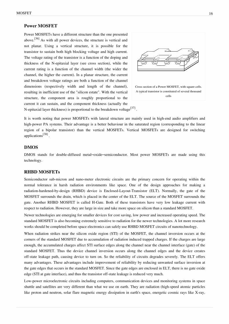
Cross section of a Power MOSFET, with square cells.A typical transistor is constituted of several thousand
cells
Power MOSFETs have a different structure than the one presentedabove.[36] As with all power devices, the structure is vertical andnot planar. Using a vertical structure, it is possible for thetransistor to sustain both high blocking voltage and high current.The voltage rating of the transistor is a function of the doping andthickness of the N-epitaxial layer (see cross section), while thecurrent rating is a function of the channel width (the wider thechannel, the higher the current). In a planar structure, the currentand breakdown voltage ratings are both a function of the channeldimensions (respectively width and length of the channel),resulting in inefficient use of the "silicon estate". With the verticalstructure, the component area is roughly proportional to thecurrent it can sustain, and the component thickness (actually theN-epitaxial layer thickness) is proportional to the breakdown voltage[37] .
It is worth noting that power MOSFETs with lateral structure are mainly used in high-end audio amplifiers andhigh-power PA systems. Their advantage is a better behaviour in the saturated region (corresponding to the linearregion of a bipolar transistor) than the vertical MOSFETs. Vertical MOSFETs are designed for switchingapplications[38] .
DMOSDMOS stands for double-diffused metal–oxide–semiconductor. Most power MOSFETs are made using thistechnology.
RHBD MOSFETsSemiconductor sub-micron and nano-meter electronic circuits are the primary concern for operating within thenormal tolerance in harsh radiation environments like space. One of the design approaches for making aradiation-hardened-by-design (RHBD) device is Enclosed-Layout-Transistor (ELT). Normally, the gate of theMOSFET surrounds the drain, which is placed in the center of the ELT. The source of the MOSFET surrounds thegate. Another RHBD MOSFET is called H-Gate. Both of these transistors have very low leakage current withrespect to radiation. However, they are large in size and take more space on silicon than a standard MOSFET.Newer technologies are emerging for smaller devices for cost saving, low power and increased operating speed. Thestandard MOSFET is also becoming extremely sensitive to radiation for the newer technologies. A lot more researchworks should be completed before space electronics can safely use RHBD MOSFET circuits of nanotechnology.When radiation strikes near the silicon oxide region (STI) of the MOSFET, the channel inversion occurs at thecorners of the standard MOSFET due to accumulation of radiation induced trapped charges. If the charges are largeenough, the accumulated charges affect STI surface edges along the channel near the channel interface (gate) of thestandard MOSFET. Thus the device channel inversion occurs along the channel edges and the device createsoff-state leakage path, causing device to turn on. So the reliability of circuits degrades severely. The ELT offersmany advantages. These advantages include improvement of reliability by reducing unwanted surface inversion atthe gate edges that occurs in the standard MOSFET. Since the gate edges are enclosed in ELT, there is no gate oxideedge (STI at gate interface), and thus the transistor off-state leakage is reduced very much.Low-power microelectronic circuits including computers, communication devices and monitoring systems in spaceshuttle and satellites are very different than what we use on earth. They are radiation (high-speed atomic particleslike proton and neutron, solar flare magnetic energy dissipation in earth's space, energetic cosmic rays like X-ray,

MOSFET 17
Gamma-ray etc.) tolerant circuits. These special electronics are designed by applying very different techniques usingRHBD MOSFETs to ensure the safe space journey and also space-walk of astronauts.
MOSFET analog switchMOSFET analog switches use the MOSFET channel as a low–on-resistance switch to pass analog signals when on,and as a high impedance when off. Signals flow in both directions across a MOSFET switch. In this application thedrain and source of a MOSFET exchange places depending on the voltages of each electrode compared to that of thegate. For a simple MOSFET without an integrated diode, the source is the more negative side for an N-MOS or themore positive side for a P-MOS. All of these switches are limited on what signals they can pass or stop by theirgate-source, gate-drain and source-drain voltages, and source-to-drain currents; exceeding the voltage limits willpotentially damage the switch.
Single-type MOSFET switchThis analog switch uses a four-terminal simple MOSFET of either P or N type. In the case of an N-type switch, thebody is connected to the most negative supply (usually GND) and the gate is used as the switch control. Wheneverthe gate voltage exceeds the source voltage by at least a threshold voltage, the MOSFET conducts. The higher thevoltage, the more the MOSFET can conduct. An N-MOS switch passes all voltages less than (Vgate–Vtn). When theswitch is conducting, it typically operates in the linear (or Ohmic) mode of operation, since the source and drainvoltages will typically be nearly equal.In the case of a P-MOS, the body is connected to the most positive voltage, and the gate is brought to a lowerpotential to turn the switch on. The P-MOS switch passes all voltages higher than (Vgate+|Vtp|). Threshold voltage(Vtp) is typically negative in the case of P-MOS.A P-MOS switch will have about three times the resistance of an N-MOS device of equal dimensions becauseelectrons have about three times the mobility of holes in silicon.
Dual-type (CMOS) MOSFET switchThis "complementary" or CMOS type of switch uses one P-MOS and one N-MOS FET to counteract the limitationsof the single-type switch. The FETs have their drains and sources connected in parallel, the body of the P-MOS isconnected to the high potential (VDD) and the body of the N-MOS is connected to the low potential (Gnd). To turnthe switch on the gate of the P-MOS is driven to the low potential and the gate of the N-MOS is driven to the highpotential. For voltages between (VDD–Vtn) and (Gnd+Vtp) both FETs conduct the signal, for voltages less than(Gnd+Vtp) the N-MOS conducts alone and for voltages greater than (VDD–Vtn) the P-MOS conducts alone.The only limits for this switch are the gate-source, gate-drain and source-drain voltage limits for both FETs. Also,the P-MOS is typically three times the width of the N-MOS so the switch will be balanced.Tri-state circuitry sometimes incorporates a CMOS MOSFET switch on its output to provide for a low ohmic, fullrange output when on and a high ohmic, mid level signal when off.

MOSFET 18
See also• BSIM• Transistor models
Literature• Dr. Ulrich Nicolai, Dr. Tobias Reimann, Prof. Jürgen Petzoldt, Josef Lutz: Application Manual IGBT and
MOSFET Power Modules, 1. Edition, ISLE Verlag, 1998, ISBN 3-932633-24-5 PDF-Version [39]
External links• An introduction to depletion-mode MOSFETs [40]
• Power MOSFETs [41]
• MOSFET Process Step by Step [42] A Flash slide showing the fabricating process of a MOSFET in detail step• MOSFET Calculator [43] MOSFET Calculator• Advanced MOSFET Issues [44]• MOSFET applet [45] Very nice applet that helps to understand MOSFET.• MIT OpenCourseWare courses:
• MIT Open Courseware 6.002 - Spring 2007 [46] -- Link to the intro electrical engineering course at MIT oncircuits and electronics.
• MIT Open Courseware 6.012 - Fall 2005 [47] -- Link to a more advanced class taught at MIT all aboutmicroelectronics and MOSFETs
• Georgia Tech BJT and FET Slides [48] Slides from a Microelectronic Circuits class at Georgia Tech• CircuitDesign: MOS Diffusion Parasitics [49] Crude illustrations of MOS diffusion structure and sample circuit
layouts to minimize their parasitics• Course on Physics of Nanoscale Transistors [50]
• Notes on Ballistic MOSFETs by Dr. Lundstrom [51] nice resource to understand theory of ballistic MOSFETs.
References[1] "Intel 45nm Hi-k Silicon Technology" (http:/ / www. intel. com/ technology/ architecture-silicon/ 45nm-core2/ index. htm). .[2] "Using a MOSFET as a Switch" (http:/ / brunningsoftware. co. uk/ FET. htm). . 090507 brunningsoftware.co.uk[3] P R Gray, P J Hurst, S H Lewis, and R G Meyer (2001). Analysis and Design of Analog Integrated Circuits (http:/ / worldcat. org/ isbn/
0471321680) (Fourth Edition ed.). New York: Wiley. pp. 66–67. ISBN 0-471-32168-0. .[4] P. R. van der Meer, A. van Staveren, A. H. M. van Roermund (2004). Low-Power Deep Sub-Micron CMOS Logic: Subthreshold Current
Reduction (http:/ / books. google. com/ books?id=nyken8ivkb8C& pg=PA78& dq=weak+ inversion&sig=SwYg44W-tRbG1cSjQBemdM22PgU). Dordrecht: Springer. p. 78. ISBN 1402028482. .
[5] Leslie S. Smith, Alister Hamilton (1998). Neuromorphic Systems: Engineering Silicon from Neurobiology (http:/ / books. google. com/books?id=kWSXEHyQL9sC& pg=PA55& dq=subthreshold+ "+ current+ mirror"& as_brr=0&sig=SklZWp6j9atrSzuvn9cbW37udMo#PPA52,M1). World Scientific. pp. 52–56. ISBN 9810233779. .
[6] Satish Kumar (2004). Neural Networks: A Classroom Approach (http:/ / books. google. com/ books?id=GJQh-2p6TvgC& pg=PA688&dq=neuromorphic+ "subthreshold+ MOS"& as_brr=0& sig=kCr306oIZOqnx49D4Sbf5PUJay0). Tata McGraw-Hill. p. 688.ISBN 0070482926. .
[7] Manfred Glesner, Peter Zipf, Michel Renovell (2002). Field-programmable Logic and Applications: 12th International Conference (http:/ /books. google. com/ books?id=fneXs6IY2-oC& pg=PA425& dq=analog+ array+ subthreshold& as_brr=0&sig=pZhV3OYe7YSvlwiF7DfmVj2Ir0w). Dordrecht: Springer. p. 425. ISBN 3540441085. .
[8] Eric A. Vittoz (1996). "The Fundamentals of Analog Micropower Design" (http:/ / books. google. com/ books?id=WTInL9njOKAC&pg=PA367& dq=weak-inversion+ maximum+ transconductance& as_brr=3& ei=o_OpSoSGN5XgNfO3vYgK#v=onepage&q=weak-inversion maximum transconductance& f=false). in Chris Toumazou, Nicholas C. Battersby, and Sonia Porta. Circuits and systemstutorials. John Wiley and Sons. pp. 365–372. ISBN 9780780311701. .
[9] Sandeep K. Shukla, R. Iris Bahar (2004). Nano, Quantum and Molecular Computing (http:/ / books. google. com/books?id=lLvo1iMGhJgC& pg=PA10& dq=subthreshold+ "process+ variation"& as_brr=0& sig=-oK8URqQwvDqmxjr7V4bhuOBtS4).Springer. p. 10 and Fig. 1.4, p. 11. ISBN 1402080670. .

MOSFET 19
[10] Ashish Srivastava, Dennis Sylvester, David Blaauw (2005). Statistical Analysis and Optimization For VLSI: Timing and Power (http:/ /books. google. com/ books?id=WqsQTyOu5jwC& pg=PA9& dq="variation+ in+ leakage+ current"& as_brr=0&sig=6cHT1H0G-PnNvk0bE7zPYViDSjU#PPA135,M1). Springer. p. 135. ISBN 0387257381. .
[11] C Galup-Montoro & Schneider MC (2007). MOSFET modeling for circuit analysis and design (http:/ / worldcat. org/ isbn/ 981-256-810-7).London/Singapore: World Scientific. pp. 83. ISBN 981-256-810-7. .
[12] Norbert R Malik (1995). Electronic circuits: analysis, simulation, and design (http:/ / worldcat. org/ isbn/ 0-02-374910-5). EnglewoodCliffs, NJ: Prentice Hall. pp. 315–316. ISBN 0-02-374910-5. .
[13] A. S. Sedra and K.C. Smith (2004). Microelectronic circuits (http:/ / worldcat. org/ isbn/ 0-19-514251-9) (Fifth Edition ed.). New York:Oxford. p. 552. ISBN 0-19-514251-9. .
[14] A. S. Sedra and K.C. Smith. p. 250, Eq. 4.14 (http:/ / worldcat. org/ isbn/ 0-19-514251-9). ISBN 0-19-514251-9. .[15] Body effect (http:/ / equars. com/ ~marco/ poli/ phd/ node20. html)[16] "1960 – Metal Oxide Semiconductor (MOS) Transistor Demonstrated: John Atalla and Dawon Kahng fabricate working transistors and
demonstrate the first successful MOS field-effect amplifier (U.S. Patent 3,102,230 filed in 1960, issued in 1963)" (http:/ / www.computerhistory. org/ semiconductor/ timeline/ 1960-MOS. html). .
[17] Computer History Museum - The Silicon Engine "Conception of the Junction Transistor" (http:/ / www. computerhistory. org/semiconductor/ timeline/ 1948-conception. html). 1948. Computer History Museum - The Silicon Engine.
[18] Computer History Museum - The Silicon Engine | 1955 - Photolithography Techniques Are Used to Make Silicon Devices (http:/ / www.computerhistory. org/ semiconductor/ timeline/ 1955-Photolithography. html)
[19] Computer History Museum - The Silicon Engine | 1963 - Complementary MOS Circuit Configuration is Invented (http:/ / www.computerhistory. org/ semiconductor/ timeline/ 1963-CMOS. html)
[20] Computer History Museum - Exhibits - Microprocessors (http:/ / www. computerhistory. org/ microprocessors/ )[21] "International Technology Roadmap for Semiconductors" (http:/ / www. itrs. net). .[22] "1965 – “Moore's Law” Predicts the Future of Integrated Circuits" (http:/ / www. computerhistory. org/ semiconductor/ timeline/
1965-Moore. html). Computer History Museum. .[23] Kaushik Roy, Kiat Seng Yeo (2004). Low Voltage, Low Power VLSI Subsystems (http:/ / books. google. com/ books?id=jXm4pNxCSCYC&
printsec=frontcover& dq=subthreshold+ mosfet+ "static+ power"& as_brr=0& sig=gr4ovBNlI9i-IafjcoHio7vmvpQ#PPA44,M1).McGraw-Hill Professional. Fig. 2.1, p. 44. ISBN 007143786X. .
[24] Kaushik Roy, Kiat Seng Yeo (2004). Low Voltage, Low Power VLSI Subsystems (http:/ / books. google. com/ books?id=jXm4pNxCSCYC&pg=PA4& dq=Energy+ switching+ "ITRS+ Projection"& as_brr=0& sig=OSs1R-OzbVgLa_4pC0do1pkaZeo). McGraw-Hill Professional.Fig. 1.1, p. 4. ISBN 007143786X. .
[25] Dragica Vasileska, Stephen Goodnick (2006). Computational Electronics (http:/ / books. google. com/ books?id=DBPnzqy5Fd8C&pg=PA103& dq=MOSFET+ half+ "+ total+ power+ consumption"& as_brr=0& sig=DVaR6DvP9YxlNQSwcyvTgwpum3s). Morgan &Claypool. p. 103. ISBN 1598290568. .
[26] http:/ / frontiersemi. com/ pdf/ papers/ RsLransist. pdf Frontier Semiconductor Paper[27] Wai-Kai Chen (2006). The VLSI Handbook (http:/ / books. google. com/ books?id=NDdsjtTLTd0C& pg=PT49& lpg=PT49& dq=halo+
"junction+ leakage"& source=web& ots=a-sCYYSP0k& sig=ZvFajEiopwY89nT05YTmX114Lf4#PPT49,M1). CRC Press. Fig. 2.28, p.2–22. ISBN 084934199X. .
[28] A Comparison Of Spike, Flash, Sper and Laser Annealing For 45nm CMOS: http:/ / www. mrs. org/ s_mrs/ sec_subscribe. asp?CID=2593&DID=109911& action=detail
[29] VLSI wiring capacitance http:/ / www. research. ibm. com/ journal/ rd/ 293/ ibmrd2903G. pdf[30] D Soudris, P Pirsch, E Barke (Editors) (2000). Integrated Circuit Design: Power and Timing Modeling, Optimization, and Simulation (10th
Int. Workshop) (http:/ / books. google. com/ books?id=TGQxMLsGzVUC& pg=PA38& lpg=PA38& dq="wiring+ capacitance"&source=web& ots=LTtgLKbRWu& sig=jTNMBOyqtBpgkD7JbodM2YQ0TI8). Springer. p. 38. ISBN 3540410686. .
[31] http:/ / www. vishay. com/ mosfets/ thermasim/ .[32] Michael Orshansky, Sani Nassif, Duane Boning (2007). Design for Manufacturability And Statistical Design: A Constructive Approach
(http:/ / www. amazon. com/ gp/ reader/ 0387309284/ ref=sib_dp_pt/ 002-1766819-0058402#reader-link). New York 309284: Springer. .[33] Jean-Pierre Colinge, Cynthia A. Colinge (2002). Physics of Semiconductor Devices (http:/ / books. google. com/
books?id=ZcDE-ENKh2gC& pg=PA233& dq=halo+ MOSFET& as_brr=0& sig=q_IW6haw9G9-rBh9E_d-i7rDbFc). Dordrecht: Springer.p. 233, Figure 7.46. ISBN 1402070187. .
[34] Eicke R. Weber, Jarek Dabrowski (Editors) (2004). Predictive Simulation of Semiconductor Processing: Status and Challenges (http:/ /books. google. com/ books?id=oCH9tiY7VeoC& pg=PA5& dq=MOSFET+ "raised+ source"& as_brr=0&sig=61g3_KAMiwEtaSq_zKnt6JPqJjo). Dordrecht: Springer. p. 5, Figure 1.2. ISBN 3540204814. .
[35] http:/ / www. techweb. com/ encyclopedia/ imageFriendly. jhtml;?term=depletion+ mode[36] Power Semiconductor Devices, B. Jayant Baliga, PWS publishing Company, Boston. ISBN 0-534-94098-6[37] http:/ / www. element-14. com/ community/ docs/ DOC-18273/ l/
power-mosfet-basics-understanding-mosfet-characteristics-associated-with-the-figure-of-merit[38] http:/ / www. element-14. com/ community/ docs/ DOC-18275/ l/
power-mosfet-basics-understanding-gate-charge-and-using-it-to-assess-switching-performance[39] http:/ / www. semikron. com/ skcompub/ en/ application_manual-193. htm

MOSFET 20
[40] http:/ / www. automotivedesignline. com/ showArticle. jhtml;?articleID=191900470[41] http:/ / www. alpha-europe. de/ microelectronics-products/ dmos-transistors/[42] http:/ / www. ece. byu. edu/ cleanroom/ virtual_cleanroom. parts/ MOSFETProcess. html[43] http:/ / www. ece. byu. edu/ cleanroom/ MOSFET_calc. phtml[44] http:/ / ece-www. colorado. edu/ ~bart/ book/ book/ chapter7/ ch7_7. htm#7_7_7[45] http:/ / www-g. eng. cam. ac. uk/ mmg/ teaching/ linearcircuits/ mosfet. html[46] http:/ / ocw. mit. edu/ OcwWeb/ Electrical-Engineering-and-Computer-Science/ 6-002Spring-2007/ CourseHome/ index. htm[47] http:/ / ocw. mit. edu/ OcwWeb/ Electrical-Engineering-and-Computer-Science/ 6-012Fall-2005/ CourseHome/ index. htm[48] http:/ / users. ece. gatech. edu/ ~alan/ index_files/ ECE3040Lecture. htm[49] http:/ / www. circuitdesign. info/ blog/ 2008/ 12/ mos-diffusion-parasitics/[50] http:/ / nanohub. org/ resources/ 5306[51] http:/ / nanohub. org/ resources/ 489

Article Sources and Contributors 21
Article Sources and ContributorsMOSFET Source: http://en.wikipedia.org/w/index.php?oldid=382382065 Contributors: A.Kurtz, Ace of Risk, AdShea, Adam1213, Adamrush, Adams13, Adma84, Adpete, Alai, Alansohn,Alexius08, Altenmann, Alureiter, Amir buet, Andonic, Angryknome94, Anoopm, Argon233, Armstrong1113149, Arnero, ArséniureDeGallium, Beatnik8983, Benandorsqueaks, Bhadani, Biezl,Bittermand, Blixtra.org, Bobo192, Bodnotbod, Brews ohare, Brim, Camrn86, Caragpietro, Ccrrccrr, Chowbok, Cmdrjameson, Congruence, Cpl Syx, Cxw, Cyferz, CyrilB, Daisydaisy, DanielChristensen, Dark Enigma, Dash69, Dbroadwell, Dftb, Dgies, Dicklyon, Donarreiskoffer, Duk, Dysprosia, Ejay, EleanorRugby, Electron9, EncMstr, Enum, Foobaz, Fred the Oyster,Fuhghettaboutit, Gdo01, Gene Nygaard, Ghost.b88, Givegains, Glenn, GoingBatty, Gorotdi, Gsjonesii, Gustengren, Hillbrand, Hooperbloob, HorsePunchKid, II MusLiM HyBRiD II, Ianis G.Vasilev, Inbamkumar86, InvertRect, J. Finkelstein, J.delanoy, JForget, Jaan513, Jaganath, Jaraalbe, Jasonlor, Jcmaco, Jeff3000, Jkl, Jmn100, John, John2kx, JohnCD, Jordsan, Jp314159, KJS77,Kevy999, Kingpin13, Kjkolb, Knutux, Kymacpherson, Labateml, Lamro, Lcarsdata, Leuko, Limsoup, Lindosland, Lindseyrose, Ll0l00l, LouScheffer, M1ss1ontomars2k4, MER-C, MIT Trekkie,MK8, Maarschalk, Magister Mathematicae, Mako098765, Mani1, Marek69, Matanbz, Materialscientist, Matt B., Matt Britt, Matt13, Maury Markowitz, Maxis ftw, Mboverload, Mebden,Melchoir, Michael Hardy, Mike R, Mike1024, Mpa, Mxn, MysticMetal, NYCJosh, Nabla, Naturalion, Navidazizi, Neparis, NitAnts, Noodle snacks, Norkimes, Nádvorník, Oh2mqk, Ok2ptp, OliFilth, Omegatron, OranL, Ot, Pankajangral3, Pejman47, Pfalstad, Pgadfor, Pieter Kuiper, Pinktulip, Pjacobi, Plugwash, Pmdboi, Potatoswatter, Qdr, Quibik, RHaworth, Rdemeis, Rdsmith4,Rogerbrent, Rumiton, Semiwiki, Senator Palpatine, Shaddack, Shadowjams, Shanes, Sietse Snel, SimonP, Sincerly, Sam, Sketerpot, Slarson, Snafflekid, SpaceFlight89, Speedevil, Spoon!, StevenHepting, Stevertigo, Stewartadcock, Stokerm, Stonecold21, SummitWulf, TRay ECE, Tangotango, TheDoober, Theterabyteboy, Trev M, Twisp, Urhixidur, Vriullop, Vvavisnotwav, Waggers,Wangi, Whiteflye, Wikid77, Wimt, Wtshymanski, Yuma, Ywaz, Zazou, Zimbricchio, Пика Пика, ۩۩, 529 anonymous edits
Image Sources, Licenses and ContributorsImage:D2PAK.JPG Source: http://en.wikipedia.org/w/index.php?title=File:D2PAK.JPG License: Creative Commons Attribution-Sharealike 2.5 Contributors: CyrilB, Geofrog, Inductiveload,Tothwolf, 1 anonymous editsFile:MOSFET functioning body.svg Source: http://en.wikipedia.org/w/index.php?title=File:MOSFET_functioning_body.svg License: GNU Free Documentation License Contributors:User:BiezlImage:Threshold formation.gif Source: http://en.wikipedia.org/w/index.php?title=File:Threshold_formation.gif License: Public Domain Contributors: Saumitra R Mehrotra & GerhardKlimeckImage:MOSFETs.jpg Source: http://en.wikipedia.org/w/index.php?title=File:MOSFETs.jpg License: Public Domain Contributors: Original uploader was Dicklyon at en.wikipediaImage:JFET P-Channel Labelled.svg Source: http://en.wikipedia.org/w/index.php?title=File:JFET_P-Channel_Labelled.svg License: Public Domain Contributors: jjbeardImage:IGFET P-Ch Enh Labelled.svg Source: http://en.wikipedia.org/w/index.php?title=File:IGFET_P-Ch_Enh_Labelled.svg License: Public Domain Contributors: jjbeardImage:IGFET P-Ch Enh Labelled simplified.svg Source: http://en.wikipedia.org/w/index.php?title=File:IGFET_P-Ch_Enh_Labelled_simplified.svg License: unknown Contributors:User:OmegatronImage:Mosfet P-Ch Sedra.svg Source: http://en.wikipedia.org/w/index.php?title=File:Mosfet_P-Ch_Sedra.svg License: Creative Commons Attribution-Sharealike 3.0 Contributors:User:Omegatron, User:PfalstadImage:IGFET P-Ch Dep Labelled.svg Source: http://en.wikipedia.org/w/index.php?title=File:IGFET_P-Ch_Dep_Labelled.svg License: Public Domain Contributors: jjbeardImage:JFET N-Channel Labelled.svg Source: http://en.wikipedia.org/w/index.php?title=File:JFET_N-Channel_Labelled.svg License: Public Domain Contributors: jjbeardImage:IGFET N-Ch Enh Labelled.svg Source: http://en.wikipedia.org/w/index.php?title=File:IGFET_N-Ch_Enh_Labelled.svg License: Public Domain Contributors: Cepheiden, Deadstar,Jjbeard, Zedh, 4 anonymous editsImage:IGFET N-Ch Enh Labelled simplified.svg Source: http://en.wikipedia.org/w/index.php?title=File:IGFET_N-Ch_Enh_Labelled_simplified.svg License: unknown Contributors:User:OmegatronImage:Mosfet N-Ch Sedra.svg Source: http://en.wikipedia.org/w/index.php?title=File:Mosfet_N-Ch_Sedra.svg License: Creative Commons Attribution-Sharealike 3.0 Contributors:User:Omegatron, User:PfalstadImage:IGFET N-Ch Dep Labelled.svg Source: http://en.wikipedia.org/w/index.php?title=File:IGFET_N-Ch_Dep_Labelled.svg License: Public Domain Contributors: jjbeardImage:mosfet n-ch circuit.svg Source: http://en.wikipedia.org/w/index.php?title=File:Mosfet_n-ch_circuit.svg License: Creative Commons Attribution-Sharealike 3.0 Contributors:User:Electron9, User:Fred the OysterImage:MOS Capacitor.svg Source: http://en.wikipedia.org/w/index.php?title=File:MOS_Capacitor.svg License: GNU Free Documentation License Contributors: User:Brews ohare, User:Fredthe OysterImage:N-channel enhancement-type MOSFET.svg Source: http://en.wikipedia.org/w/index.php?title=File:N-channel_enhancement-type_MOSFET.svg License: Public Domain Contributors:User:Fred the Oyster, User:Hermitage17Image:N-channel mosfet.svg Source: http://en.wikipedia.org/w/index.php?title=File:N-channel_mosfet.svg License: Public Domain Contributors: User:Fred the Oyster, User:Hermitage17Image:IvsV mosfet.png Source: http://en.wikipedia.org/w/index.php?title=File:IvsV_mosfet.png License: GNU Free Documentation License Contributors: CyrilB, WikipediaMaster, 1anonymous editsImage:Mosfet linear.svg Source: http://en.wikipedia.org/w/index.php?title=File:Mosfet_linear.svg License: Creative Commons Attribution-Sharealike 2.5 Contributors: User:CyrilBImage:Mosfet saturation.svg Source: http://en.wikipedia.org/w/index.php?title=File:Mosfet_saturation.svg License: Creative Commons Attribution-Sharealike 2.5 Contributors: Cepheiden,CyrilB, WikipediaMasterImage:MOSFET functioning body.svg Source: http://en.wikipedia.org/w/index.php?title=File:MOSFET_functioning_body.svg License: GNU Free Documentation License Contributors:User:BiezlImage:Intel gate length trend.PNG Source: http://en.wikipedia.org/w/index.php?title=File:Intel_gate_length_trend.PNG License: Creative Commons Attribution-Sharealike 3.0 Contributors:Naturalion, 1 anonymous editsImage:WIde-swing MOSFET mirror.PNG Source: http://en.wikipedia.org/w/index.php?title=File:WIde-swing_MOSFET_mirror.PNG License: GNU Free Documentation License Contributors: User:Brews ohareFile:Transistor.jpg Source: http://en.wikipedia.org/w/index.php?title=File:Transistor.jpg License: Creative Commons Attribution 3.0 Contributors: User:Daniel ChristensenImage:MOSFET junction structure.png Source: http://en.wikipedia.org/w/index.php?title=File:MOSFET_junction_structure.png License: GNU Free Documentation License Contributors:User:Brews ohareImage:Doublegate FinFET.PNG Source: http://en.wikipedia.org/w/index.php?title=File:Doublegate_FinFET.PNG License: GNU Free Documentation License Contributors: Original uploaderwas Irene Ringworm at en.wikipediaImage:Power mos cell layout.svg Source: http://en.wikipedia.org/w/index.php?title=File:Power_mos_cell_layout.svg License: GNU Free Documentation License Contributors: CyrilBUTTAY
LicenseCreative Commons Attribution-Share Alike 3.0 Unportedhttp:/ / creativecommons. org/ licenses/ by-sa/ 3. 0/


![BAB II TINJAUAN PUSTAKAeprints.umm.ac.id/35672/3/jiptummpp-gdl-arirobiuli-48901... · 2017-11-14 · 10 Gambar 2.6 Simbol Transistor MOSFET Mode Enhancement [9]. (a). N-Channel Enhancement](https://static.fdocuments.in/doc/165x107/5e9da1fd111da33d79475dc0/bab-ii-tinjauan-2017-11-14-10-gambar-26-simbol-transistor-mosfet-mode-enhancement.jpg)


