JESD204C Intel® Agilex™ FPGA IP Design Example …...2. JESD204C Intel FPGA IP Design Example...
26
JESD204C Intel ® Agilex ™ FPGA IP Design Example User Guide Updated for Intel ® Quartus ® Prime Design Suite: 19.3 IP Version: 1.0.0 Subscribe Send Feedback UG-20257 | 2019.10.23 Latest document on the web: PDF | HTML
Transcript of JESD204C Intel® Agilex™ FPGA IP Design Example …...2. JESD204C Intel FPGA IP Design Example...

JESD204C Intel® Agilex™ FPGA IPDesign Example User Guide
Updated for Intel® Quartus® Prime Design Suite: 19.3
IP Version: 1.0.0
SubscribeSend Feedback
UG-20257 | 2019.10.23Latest document on the web: PDF | HTML

Contents
1. About the JESD204C Intel® Agilex™ FPGA IP Design Example User Guide.......................3
2. JESD204C Intel FPGA IP Design Example Quick Start Guide........................................... 62.1. Design Example Block Diagram............................................................................... 72.2. Hardware and Software Requirements...................................................................... 82.3. Generating the Design............................................................................................8
2.3.1. Design Example Parameters........................................................................82.3.2. Directory Structure.................................................................................. 10
2.4. Compiling and Simulating the Design......................................................................12
3. Detailed Description for the JESD204C Design Example................................................143.1. System Components............................................................................................ 14
3.1.1. JTAG to Avalon® Master Bridge.................................................................. 153.1.2. Parallel I/O (PIO) Core..............................................................................153.1.3. SPI Master.............................................................................................. 163.1.4. SYSREF Generator................................................................................... 163.1.5. Pattern Generator and Checker.................................................................. 18
3.2. Design Example Clock and Reset............................................................................193.3. Design Example Signals........................................................................................213.4. JESD204C Design Example Control Registers........................................................... 23
4. Document Revision History for the JESD204C Intel Agilex FPGA IP DesignExample User Guide.................................................................................................26
Contents
JESD204C Intel® Agilex™ FPGA IP Design Example User Guide Send Feedback
2

1. About the JESD204C Intel® Agilex™ FPGA IP DesignExample User Guide
This user guide provides the features, usage guidelines, and detailed description aboutthe design examples for the JESD204C Intel® FPGA IP using Intel Agilex™ devices.
Intended Audience
This document is intended for:
• Design architect to make IP selection during system level design planning phase
• Hardware designers when integrating the IP into their system level design
• Validation engineers during system level simulation and hardware validation phase
Related Documents
The following table lists other reference documents which are related to the JESD204CIntel FPGA IP.
Table 1. Related Documents
Reference Description
JESD204C Intel FPGA IP User Guide Provides information about the JESD204C Intel FPGA IP.
Intel Agilex Device Data Sheet This document describes the electrical characteristics,switching characteristics, configuration specifications, andtiming for Intel Agilex devices.
Acronyms and Glossary
Table 2. Acronym List
Acronym Expansion
LEMC Local Extended Multiblock Clock
FC Frame clock rate
ADC Analog to Digital Converter
DAC Digital to Analog Converter
DSP Digital Signal Processor
TX Transmitter
RX Receiver
DLL Data link layer
CSR Control and status register
CRU Clock and Reset Unit
continued...
UG-20257 | 2019.10.23
Send Feedback
Intel Corporation. All rights reserved. Agilex, Altera, Arria, Cyclone, Enpirion, Intel, the Intel logo, MAX, Nios,Quartus and Stratix words and logos are trademarks of Intel Corporation or its subsidiaries in the U.S. and/orother countries. Intel warrants performance of its FPGA and semiconductor products to current specifications inaccordance with Intel's standard warranty, but reserves the right to make changes to any products and servicesat any time without notice. Intel assumes no responsibility or liability arising out of the application or use of anyinformation, product, or service described herein except as expressly agreed to in writing by Intel. Intelcustomers are advised to obtain the latest version of device specifications before relying on any publishedinformation and before placing orders for products or services.*Other names and brands may be claimed as the property of others.
ISO9001:2015Registered
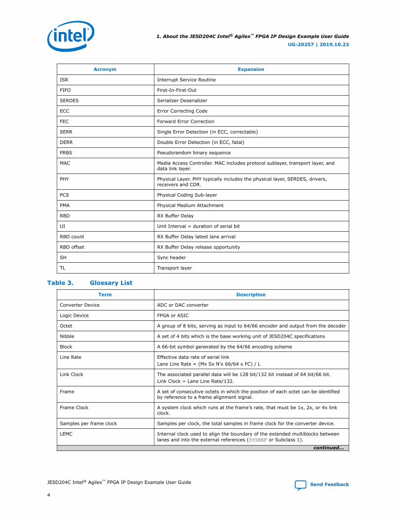
Acronym Expansion
ISR Interrupt Service Routine
FIFO First-In-First-Out
SERDES Serializer Deserializer
ECC Error Correcting Code
FEC Forward Error Correction
SERR Single Error Detection (in ECC, correctable)
DERR Double Error Detection (in ECC, fatal)
PRBS Pseudorandom binary sequence
MAC Media Access Controller. MAC includes protocol sublayer, transport layer, anddata link layer.
PHY Physical Layer. PHY typically includes the physical layer, SERDES, drivers,receivers and CDR.
PCS Physical Coding Sub-layer
PMA Physical Medium Attachment
RBD RX Buffer Delay
UI Unit Interval = duration of serial bit
RBD count RX Buffer Delay latest lane arrival
RBD offset RX Buffer Delay release opportunity
SH Sync header
TL Transport layer
Table 3. Glossary List
Term Description
Converter Device ADC or DAC converter
Logic Device FPGA or ASIC
Octet A group of 8 bits, serving as input to 64/66 encoder and output from the decoder
Nibble A set of 4 bits which is the base working unit of JESD204C specifications
Block A 66-bit symbol generated by the 64/66 encoding scheme
Line Rate Effective data rate of serial linkLane Line Rate = (Mx Sx N’x 66/64 x FC) / L
Link Clock The associated parallel data will be 128 bit/132 bit instead of 64 bit/66 bit.Link Clock = Lane Line Rate/132.
Frame A set of consecutive octets in which the position of each octet can be identifiedby reference to a frame alignment signal.
Frame Clock A system clock which runs at the frame's rate, that must be 1x, 2x, or 4x linkclock.
Samples per frame clock Samples per clock, the total samples in frame clock for the converter device.
LEMC Internal clock used to align the boundary of the extended multiblocks betweenlanes and into the external references (SYSREF or Subclass 1).
continued...
1. About the JESD204C Intel® Agilex™ FPGA IP Design Example User Guide
UG-20257 | 2019.10.23
JESD204C Intel® Agilex™ FPGA IP Design Example User Guide Send Feedback
4

Term Description
Subclass 0 No support for deterministic latency. Data should be immediately released uponlane to lane deskew on receiver.
Subclass 1 Deterministic latency using SYSREF.
Multipoint Link Inter-device links with 2 or more converter devices.
64B/66B Encoding Line code that maps 64-bit data to 66 bits to form a block. The base level datastructure is a block that starts with 2-bit sync header.
Table 4. Symbols
Term Description
L Number of lanes per converter device
M Number of converters per device
F Number of octets per frame on a single lane
S Number of samples transmitted per single converter per frame cycle
N Converter resolution
N’ Total number of bits per sample in the user data format
CS Number of control bits per conversion sample
CF Number of control words per frame clock period per link
HD High Density user data format
E Number of multiblocks in an extended multiblock
1. About the JESD204C Intel® Agilex™ FPGA IP Design Example User Guide
UG-20257 | 2019.10.23
Send Feedback JESD204C Intel® Agilex™ FPGA IP Design Example User Guide
5
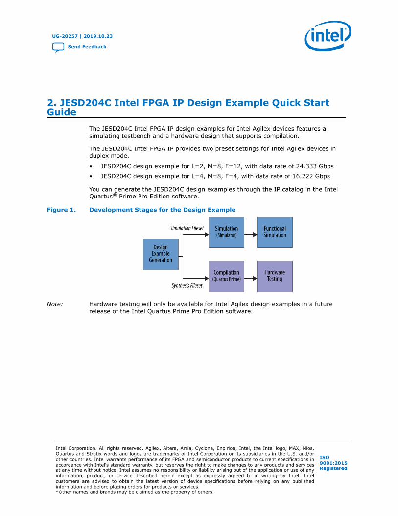
2. JESD204C Intel FPGA IP Design Example Quick StartGuide
The JESD204C Intel FPGA IP design examples for Intel Agilex devices features asimulating testbench and a hardware design that supports compilation.
The JESD204C Intel FPGA IP provides two preset settings for Intel Agilex devices induplex mode.
• JESD204C design example for L=2, M=8, F=12, with data rate of 24.333 Gbps
• JESD204C design example for L=4, M=8, F=4, with data rate of 16.222 Gbps
You can generate the JESD204C design examples through the IP catalog in the IntelQuartus® Prime Pro Edition software.
Figure 1. Development Stages for the Design Example
DesignExample
Generation
Simulation Fileset
Synthesis Fileset
Simulation(Simulator)
FunctionalSimulation
Compilation(Quartus Prime)
HardwareTesting
Note: Hardware testing will only be available for Intel Agilex design examples in a futurerelease of the Intel Quartus Prime Pro Edition software.
UG-20257 | 2019.10.23
Send Feedback
Intel Corporation. All rights reserved. Agilex, Altera, Arria, Cyclone, Enpirion, Intel, the Intel logo, MAX, Nios,Quartus and Stratix words and logos are trademarks of Intel Corporation or its subsidiaries in the U.S. and/orother countries. Intel warrants performance of its FPGA and semiconductor products to current specifications inaccordance with Intel's standard warranty, but reserves the right to make changes to any products and servicesat any time without notice. Intel assumes no responsibility or liability arising out of the application or use of anyinformation, product, or service described herein except as expressly agreed to in writing by Intel. Intelcustomers are advised to obtain the latest version of device specifications before relying on any publishedinformation and before placing orders for products or services.*Other names and brands may be claimed as the property of others.
ISO9001:2015Registered

2.1. Design Example Block Diagram
Figure 2. JESD204C Design Example High-level Block Diagram
SPI 3 Wire
Reset Release IP(ninit_done)
Reset Debounce
VCC
PatternChecker
PatternGenerator
JESD204C Intel FPGA IP (Duplex) (1) JESD204C Platform Designer System
ED Control
IOPLL
PIO IN and OUT
SPI
Reset Sequencer
JTAG to AvalonMaster Bridge
JESD204CDuplex PHY
Transceiver ResetController and PLL
JESD204C TX
tx/rx_reconfig_clk
refclk_core
refclk_xcvr
TX Serial Data
RX Serial Data
Note: 1. The JESD204C IP is part of the Platform Designer system.2. For demonstration purposes, the design example is loopbacked. You can modify the design and connect to external converters.
in_sysref sysref_out
SYSREFGenerator
mgmt_clk
global_rst
To Host Computer(JTAG/Platform Designer)
Loopbackin Simulation Testbench (2)
tx/rx_frame_clktx/rx_link_clk
tx/rx_phase
JESD204C RX
The design example consists of the following modules:
• Platform Designer system
— JESD204C Intel FPGA IP
— JTAG to Avalon master bridge
— Parallel I/O (PIO) controller
— Serial Port Interface (SPI)—master module
— Core PLL
— SYSREF generator
• Pattern generator
• Pattern checker
• IOPLL
Table 5. Design Example Modules
Components Description
Platform Designer system The Platform Designer system instantiates the JESD204C IP data pathand supporting peripherals.
JESD204C Intel FPGA IP This Platform Designer subsystem contains the TX and RX JESD204C IPsinstantiated together with the duplex PHY.
JTAG to Avalon Master bridge This bridge provides system console host access to the memory-mappedIP in the design through the JTAG interface.
Parallel I/O (PIO) controller This controller provides a memory-mapped interface for sampling anddriving general purpose I/O ports.
SPI master This module handles the serial transfer of configuration data to the SPIinterface on the converter end.
SYSREF generator The SYSREF generator uses the link clock as a reference clock andgenerates SYSREF pulses for the JESD204C IP.Note: This design example uses the SYSREF generator to demonstrate
the duplex JESD204C IP link initialization. In the JESD204Csubclass 1 system level application, you must generate theSYSREF from the same source as the device clock.
continued...
2. JESD204C Intel FPGA IP Design Example Quick Start Guide
UG-20257 | 2019.10.23
Send Feedback JESD204C Intel® Agilex™ FPGA IP Design Example User Guide
7

Components Description
Pattern generator The pattern generator generates a PRBS or ramp pattern.
Pattern checker The pattern checker verifies the PRBS or ramp pattern received, andflags an error when it finds a mismatch of data sample.
IOPLL This design example uses an IOPLL to generate a user clock fortransmitting data into the JESD204C IP.
2.2. Hardware and Software Requirements
Intel uses the following hardware and software to test the design examples in a Linuxsystem:
• Intel Quartus Prime Pro Edition software version 19.3
• ModelSim*, Xcelium*, NCSim (Verilog only), or VCS*/VCS MX simulator
2.3. Generating the Design
Start ParameterEditor
Specify IP Variationand Select Device
SelectDesign Parameters
InitiateDesign Generation
Specify Example Design
To generate the design example from the IP parameter editor:
1. Create a project targeting Intel Agilex device family and select the desired device.
2. In the IP Catalog, Tools ➤ IP Catalog, select JESD204C Intel FPGA IP.
3. Specify a top-level name and the folder for your custom IP variation. Click OK.
4. Select a design from the Presets library and click Apply. When you select adesign, the system automatically populates the IP parameters for the design.
Note: If you select another design, the settings of the IP parameters changeaccordingly. Alternatively, you can also specify your own settings andgenerate the design.
5. Under the Example Design tab, specify the design example parameters asdescribed in Design Example Parameters.
6. Click Generate Example Design.
The software generates all design files in the sub-directories. These files are requiredto run simulation and compilation.
2.3.1. Design Example Parameters
The JESD204C Intel FPGA IP parameter editor includes a Example Design tab for youto specify certain parameters before generating the design example.
2. JESD204C Intel FPGA IP Design Example Quick Start Guide
UG-20257 | 2019.10.23
JESD204C Intel® Agilex™ FPGA IP Design Example User Guide Send Feedback
8

Table 6. Parameters in the Example Design Tab
Parameter Options Description
Select Design • SystemConsoleControl
• None
Select the system console control to access the design example data paththrough the system console.
Simulation On, Off Turn on for the IP to generate the necessary files for simulating the designexample.
Synthesis On, Off Turn on for the IP to generate the necessary files for Intel Quartus Primecompilation.
HDL format (forsimulation)
Verilog only Select the HDL format of the RTL files for simulation.
HDL format (forsynthesis)
Verilog only Select the HDL format of the RTL files for synthesis.
Generate 3-wireSPI module
On, Off Turn on to enable 3-wire SPI interface instead of 4-wire.
Sysref mode • One-shot• Periodic• Gapped
periodic
Select whether you want the SYSREF alignment to be a one-shot pulse mode,periodic, or gapped periodic, based on your design requirements and timingflexibility.• One-shot: Select this option to enable SYSREF to be a one-shot pulse mode.
The sysref_ctrl[17] register bit's value is 0. After the JESD204C IP resetdeasserts, change the sysref_ctrl[17] register's value from 0 to 1, thento 0, for a one-shot SYSREF pulse.
• Periodic: SYSREF in periodic mode has 50:50 duty cycle. SYSREF period isE*SYSREF_MULP.
• Gapped periodic: SYSREF has programmable duty cycle of granularity of 1link clock cycle. SYSREF period is E*SYSREF_MULP. For out-of-range dutycycle setting, the SYSREF generation block should automatically infer 50:50duty cycle.
Refer to SYSREF Generator on page 16 for more information about the SYSREFperiod.
Select board • None Select the board for the design example.• None: This option excludes hardware aspects for the design example. All the
pin assignments will be set to virtual pins.
Test pattern • PRBS-7• PRBS-9• PRBS-15• PRBS-23• Ramp
Select the patten generator and checker test pattern to either ramp or one ofthe PRBS pattern options.The PRBS options are some of the commonly used degree of polynomials.If you select PRBS pattern, the pattern checker expects the scrambling seed tobe self-synchronized when the deskew alignment is achieved by the JESD204CRX IP.If you select ramp pattern, the first valid data sample for each converter (M) isloaded as the initial value. Subsequent data sample values must increase by 1 ineach clock cycle up to the maximum and then roll over to 0. For example, whenS=1, N=16 and WIDTH_MULP = 2, the data width per converter isS*WIDTH_MULP*N=32. The maximum data sample value is 0xFFFF.The ramp pattern checker verifies that identical patterns are received across allconverters.
Enable internalserial loopback(Simulation)
On, Off Turn on to enable internal serial loopback. If you turn on this option, the RX pathtakes the serial input from the TX path internally in the FPGA.
Enable commandchannel pattern(Simulation)
On, Off Turn on to enable command channel pattern.
2. JESD204C Intel FPGA IP Design Example Quick Start Guide
UG-20257 | 2019.10.23
Send Feedback JESD204C Intel® Agilex™ FPGA IP Design Example User Guide
9
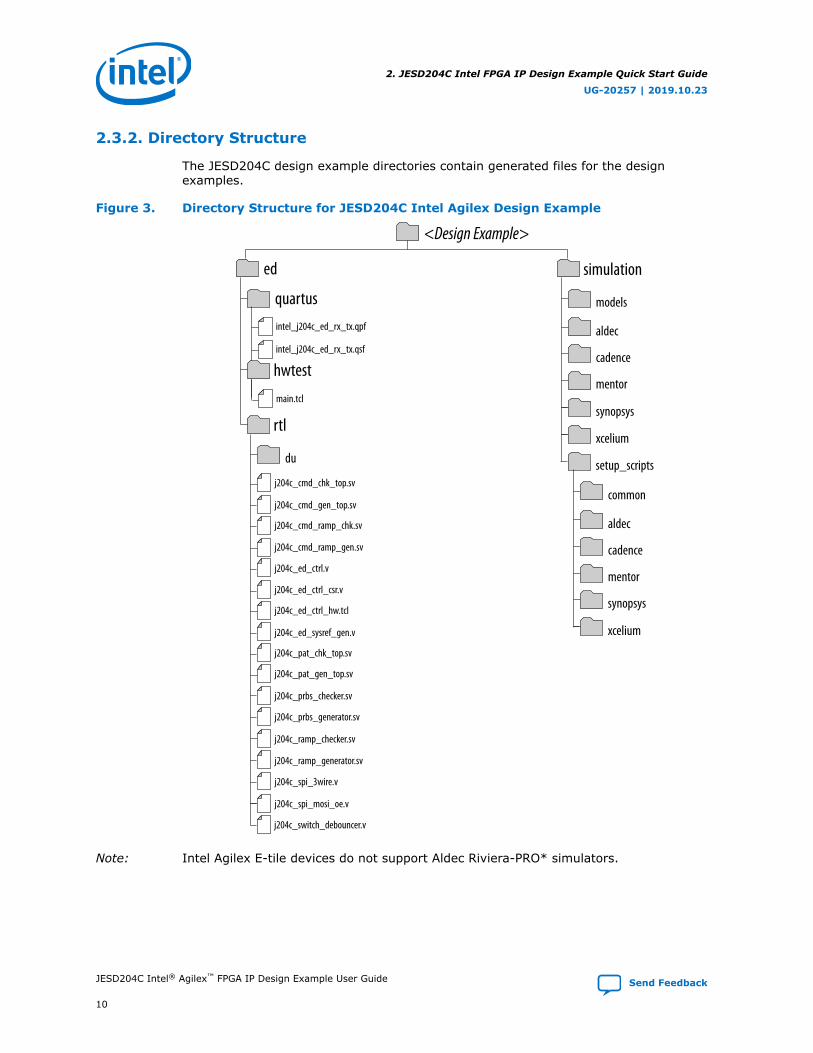
2.3.2. Directory Structure
The JESD204C design example directories contain generated files for the designexamples.
Figure 3. Directory Structure for JESD204C Intel Agilex Design Example
<Design Example>
ed simulation
models
aldec
cadence
mentor
synopsys
xcelium
setup_scripts
common
aldec
cadence
mentor
synopsys
xcelium
quartusintel_j204c_ed_rx_tx.qpf
intel_j204c_ed_rx_tx.qsf
rtl
du
j204c_cmd_gen_top.sv
j204c_cmd_chk_top.sv
j204c_ed_ctrl.v
j204c_cmd_ramp_chk.sv
j204c_cmd_ramp_gen.sv
j204c_ed_sysref_gen.v
j204c_ed_ctrl_csr.v
j204c_ed_ctrl_hw.tcl
j204c_pat_chk_top.sv
j204c_prbs_checker.sv
j204c_prbs_generator.sv
j204c_ramp_checker.sv
j204c_pat_gen_top.sv
j204c_ramp_generator.sv
j204c_spi_3wire.v
j204c_spi_mosi_oe.v
j204c_switch_debouncer.v
hwtestmain.tcl
Note: Intel Agilex E-tile devices do not support Aldec Riviera-PRO* simulators.
2. JESD204C Intel FPGA IP Design Example Quick Start Guide
UG-20257 | 2019.10.23
JESD204C Intel® Agilex™ FPGA IP Design Example User Guide Send Feedback
10

Table 7. Directory Files
Folders Files
ed/rtl • du— intel_j204c_ed_rx_tx.sv (top-level HDL file)— intel_j204c_ed_rx_tx.sdc— J204c_rx_tx_ip.qsys— j204c_rx_tx_ss.qsys— altera_s10_user_rst_clkgate_0.ip— intel_j204c_se_outbuf_1bit.ip
• rx— intel_j204c_ed_rx.sv (top-level HDL file)— intel_j204c_ed_rx.sdc— j204c_rx_ip.qsys— j204c_rx_ss.qsys— altera_s10_user_rst_clkgate_0.ip— intel_j204c_se_outbuf_1bit.ip
• tx— intel_j204c_ed_tx.sv (top-level HDL file)— intel_j204c_ed_tx.sdc— j204c_tx_ip.qsys— j204c_tx_ss.qsys— altera_s10_user_rst_clkgate_0.ip— intel_j204c_se_outbuf_1bit.ip
simulation/models • tb_top.sv
simulation/cadence • cadence_sim.sh• tb_top_wave.tcl
simulation/mentor • modelsim_sim.tcl• tb_top_waveform.do
simulation/synopsys • vcs— vcs_sim.sh— tb_top_wave_ed.do
• vcsmx— vcsmx_sim.sh— tb_top_wave_ed.do
simulation/xcelium • xcelium_sim.sh• tb_top_wave.tcl
simulation/setup_scripts/common • modelsim_files.tcl• ncsim_files.tcl• vcs_files.tcl• vcsmx_files.tcl• xcelium_files.tcl
simulation/setup_scripts/cadence • cds.lib• hdl.var• ncsim_setup.sh• <cds_libs folder>
continued...
2. JESD204C Intel FPGA IP Design Example Quick Start Guide
UG-20257 | 2019.10.23
Send Feedback JESD204C Intel® Agilex™ FPGA IP Design Example User Guide
11

Folders Files
simulation/setup_scripts/mentor • msim_setup.tcl
simulation/setup_scripts/synopsys • vcs— vcs_setup.sh
• vcsmx— vcsmx_setup.sh— synopsys_sim.setup
simulation/setup_scripts/xcelium • xcelium_setup.sh• cds.lib• hdl.var• <cds_libs folder>
2.4. Compiling and Simulating the Design
The design example testbench simulates your generated design.
Change to Testbench Directory
Run<Simulation Script>
AnalyzeResults
To simulate the design, perform the following steps:
1. Change the working directory to <example_design_directory>/simulation/<Simulator>.
2. In the command line, run the simulation script. The table below shows thecommands to run the supported simulators.
Simulator Command
NCSim sh cadence_sim.sh
ModelSim vsim -do modelsim_sim.tcl
vsim -c -do modelsim_sim.tcl (without ModelSimGUI)
VCS sh vcs_sim.sh
VCS MX sh vcsmx_sim.sh
Xcelium Parallel sh xcelium_sim.sh
The simulation ends with messages that indicate whether the run was successfulor not.
2. JESD204C Intel FPGA IP Design Example Quick Start Guide
UG-20257 | 2019.10.23
JESD204C Intel® Agilex™ FPGA IP Design Example User Guide Send Feedback
12

Figure 4. Successful SimulationThe average simulation run time including design elaboration is approximately 8 minutes on VCS, and 26minutes on ModelSim - Intel FPGA Starter Edition for preset with L=2, M=8, and F=12.
2. JESD204C Intel FPGA IP Design Example Quick Start Guide
UG-20257 | 2019.10.23
Send Feedback JESD204C Intel® Agilex™ FPGA IP Design Example User Guide
13

3. Detailed Description for the JESD204C Design ExampleThe JESD204C design example demonstrates the functionality of data streaming usingloopback mode.
You can specify the parameters settings of your choice and generate the designexample.
The design example is available only in duplex mode for both Base and PHY variant.You can choose Base only or PHY only variant but the IP would generate the designexample for both Base and PHY.
Note: Some high data rate configurations may fail timing. To avoid timing failure, considerspecifying lower frame clock frequency multiplier (FCLK_MULP) value in theConfigurations tab of the JESD204C Intel FPGA IP parameter editor.
3.1. System Components
The JESD204C design example provides a software-based control flow that uses thehard control unit with or without system console support.
The design example enables an auto link up in internal and external loopback modes.
You can either configure your own settings or use one of the two presets provided.
• L=2, M=8, F=12, with data rate of 24.333 Gbps
• L=4, M=8, F=4, with data rate of 16.222 Gbps
UG-20257 | 2019.10.23
Send Feedback
Intel Corporation. All rights reserved. Agilex, Altera, Arria, Cyclone, Enpirion, Intel, the Intel logo, MAX, Nios,Quartus and Stratix words and logos are trademarks of Intel Corporation or its subsidiaries in the U.S. and/orother countries. Intel warrants performance of its FPGA and semiconductor products to current specifications inaccordance with Intel's standard warranty, but reserves the right to make changes to any products and servicesat any time without notice. Intel assumes no responsibility or liability arising out of the application or use of anyinformation, product, or service described herein except as expressly agreed to in writing by Intel. Intelcustomers are advised to obtain the latest version of device specifications before relying on any publishedinformation and before placing orders for products or services.*Other names and brands may be claimed as the property of others.
ISO9001:2015Registered

3.1.1. JTAG to Avalon® Master Bridge
The JTAG to Avalon® Master Bridge provides a connection between the host system toaccess the memory-mapped JESD204C IP and the peripheral IP control and statusregisters through the JTAG interface.
Figure 5. System with a JTAG to Avalon Master Bridge Core
Note: System clock must be at least 2X faster than the JTAG clock. The system clock is mgmt_clk (100MHz) in thisdesign example.
Intel FPGA
JTAG to Transaction Bridge
JTAGClock
SystemClock
HostPC JTA
G
Avalo
n Mem
ory-
Map
ped M
aste
r
Syste
m In
terco
nnec
t Fab
ric
ED Control
PIO Control
PIO Status
Reset Sequencr 0
Reset Sequencer 1
SPI Master 0
JESD204CDuplex
Native PHY
JESD204C IP
JESD204C TX
JESD204C RX
Avalon Memory-Mapped Bridge
3.1.2. Parallel I/O (PIO) Core
The parallel input/output (PIO) core with Avalon interface provides a memory-mappedinterface between an Avalon Memory-Mapped slave port and general purpose I/Oports. The I/O ports connect either to on-chip user logic, or to I/O pins that connect todevices external to the FPGA.
Figure 6. PIO Core with Input Ports, Output Ports, and IRQ SupportBy default, the Platform Designer component disables the Interrupt Service Line (IRQ).
IRQ
datain
interruptmask
out
edgecapture
32
32Avalon-MMInterface to
On-chip Logic
addressdata
control
The PIO I/O ports are assigned at the top level HDL file (io_status for input ports,io_control for output ports).
The table below describes the signal connectivity for the status and control I/O portsto the DIP switch and LED on the development kit.
3. Detailed Description for the JESD204C Design Example
UG-20257 | 2019.10.23
Send Feedback JESD204C Intel® Agilex™ FPGA IP Design Example User Guide
15
Table 8. PIO Core I/O Ports
Port Bit Signal
Out_port 0 USER_LED SPI programming done
31:1 Reserved
In_port 0 USER_DIP internal serial loopback enableOff = 1On = 0
1 USER_DIP FPGA-generated SYSREF enableOff = 1On = 0
31:2 Reserved.
3.1.3. SPI Master
The SPI master module is a standard Platform Designer component in the IP Catalogstandard library. This module uses the SPI protocol to facilitate the configuration ofexternal converters (for example, ADC, DAC, and external clock generators) via astructured register space inside these devices. The SPI master has an Avalon memory-mapped interface that connects to the Avalon master (JTAG to Avalon master bridge)via the Avalon-MM interconnect. The SPI master receives configuration instructionsfrom the Avalon master.
The SPI master module controls up to 32 independent SPI slaves. The SCLK baud rateis configured to 20 MHz (divisible by 5).
This module is configured to a 4-wire, 24-bit width interface. If the Generate 3-WireSPI Module option is selected, an additional module is instantiated to convert the 4-wire output of the SPI master to 3-wire.
3.1.4. SYSREF Generator
SYSREF is a critical timing signal for data converters with JESD204C interface.
The SYSREF generator in the design example is used for the duplex JESD204C IP linkinitialization demonstration purpose only. In the JESD204C subclass 1 system levelapplication,you must generate SYSREF from the same source as the device clock.
For the JESD204C IP, the SYSREF multiplier (SYSREF_MULP) of the SYSREF controlregister defines the SYSREF period, which is n-integer multiple of the E parameter.
You must ensure E*SYSREF_MULP ≤16. For example, if E=1, the legal setting forSYSREF_MULP must be within 1–16, and if E=3, the legal setting for SYSREF_MULPmust be within 1–5.
Note: If you set an out-of-range SYSREF_MULP, the SYSREF generator will fix the setting toSYSREF_MULP=1.
You can select whether you want the SYSREF type to be a one-shot pulse, periodic, orgapped periodic through the Example Design tab in the JESD204C Intel FPGA IPparameter editor.
3. Detailed Description for the JESD204C Design Example
UG-20257 | 2019.10.23
JESD204C Intel® Agilex™ FPGA IP Design Example User Guide Send Feedback
16
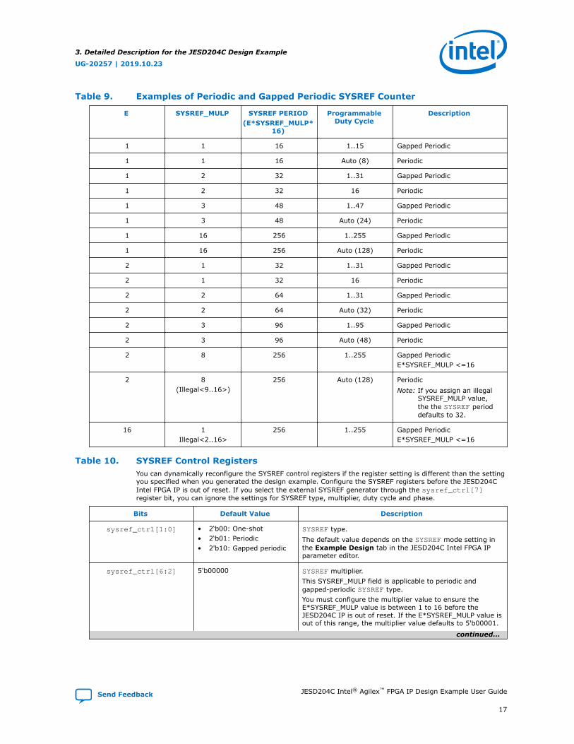
Table 9. Examples of Periodic and Gapped Periodic SYSREF Counter
E SYSREF_MULP SYSREF PERIOD(E*SYSREF_MULP*
16)
ProgrammableDuty Cycle
Description
1 1 16 1..15 Gapped Periodic
1 1 16 Auto (8) Periodic
1 2 32 1..31 Gapped Periodic
1 2 32 16 Periodic
1 3 48 1..47 Gapped Periodic
1 3 48 Auto (24) Periodic
1 16 256 1..255 Gapped Periodic
1 16 256 Auto (128) Periodic
2 1 32 1..31 Gapped Periodic
2 1 32 16 Periodic
2 2 64 1..31 Gapped Periodic
2 2 64 Auto (32) Periodic
2 3 96 1..95 Gapped Periodic
2 3 96 Auto (48) Periodic
2 8 256 1..255 Gapped PeriodicE*SYSREF_MULP <=16
2 8(Illegal<9..16>)
256 Auto (128) PeriodicNote: If you assign an illegal
SYSREF_MULP value,the the SYSREF perioddefaults to 32.
16 1Illegal<2..16>
256 1..255 Gapped PeriodicE*SYSREF_MULP <=16
Table 10. SYSREF Control RegistersYou can dynamically reconfigure the SYSREF control registers if the register setting is different than the settingyou specified when you generated the design example. Configure the SYSREF registers before the JESD204CIntel FPGA IP is out of reset. If you select the external SYSREF generator through the sysref_ctrl[7]register bit, you can ignore the settings for SYSREF type, multiplier, duty cycle and phase.
Bits Default Value Description
sysref_ctrl[1:0] • 2‘b00: One-shot• 2‘b01: Periodic• 2'b10: Gapped periodic
SYSREF type.The default value depends on the SYSREF mode setting inthe Example Design tab in the JESD204C Intel FPGA IPparameter editor.
sysref_ctrl[6:2] 5'b00000 SYSREF multiplier.This SYSREF_MULP field is applicable to periodic andgapped-periodic SYSREF type.You must configure the multiplier value to ensure theE*SYSREF_MULP value is between 1 to 16 before theJESD204C IP is out of reset. If the E*SYSREF_MULP value isout of this range, the multiplier value defaults to 5'b00001.
continued...
3. Detailed Description for the JESD204C Design Example
UG-20257 | 2019.10.23
Send Feedback JESD204C Intel® Agilex™ FPGA IP Design Example User Guide
17
Bits Default Value Description
For example:If E =1, write 5'b10000 to sysref_ctrl[6:2] to set theSYSREF_MULP decimal value of 16.
sysref_ctrl[7] • Duplex datapath: 1'b1• Simplex TX or RX
datapath: 1'b0
SYSREF select.The default value depends on the SYSREF mode setting inthe Example Design tab in the JESD204C Intel FPGA IPparameter editor.• 0: External SYSREF• 1: Internal SYSREF
sysref_ctrl[15:8] 8'h00 SYSREF duty cycle when SYSREF type is periodic or gappedperiodic.You must configure the duty cycle before the JESD204C IPis out of reset.Maximum value = (E*SYSREF_MULP*16)-1For example:50% duty cycle = (E*SYSREF_MULP*16)/2If you do not configure this register field, the duty cycledefaults to 50%.
sysref_ctrl[16] 1'b0 SYSREF phase (for sysref_out output port).• 0: Positive edge• 1: Negative edge
sysref_ctrl[17] 1'b0 Manual control when SYSREF type is one-shot.• Write 1 to set the SYSREF signal to high.• Write 0 to set the SYSREF signal to low.You need to write a 1 then a 0 to create a SYSREF pulse inone-shot mode.
sysref_ctrl[31:18] Don't Care Reserved.
3.1.5. Pattern Generator and Checker
The pattern generator and checker are useful for creating data samples andmonitoring for testing purposes.
Table 11. Supported Pattern Generator
Pattern Generator Description
PRBS pattern generator The JESD204C design example PRBS pattern generator supports thefollowing degree of polynomials:• PRBS23: X23+X18+1• PRBS15: X15+X14+1• PRBS9: X9+X5+1• PRBS7: X7+X6+1
Ramp pattern generator The ramp pattern value increments by 1 for every subsequent samplewith the generator width of N, and rolls over to 0 when all bits in thesample are 1.Enable the ramp pattern generator by writing a 1 to bit 2 of thetst_ctl register of the ED control block.
Command channel ramp pattern generator The JESD204C design example supports command channel ramp patterngenerator per lane. The ramp pattern value increments by 1 per 6 bits ofcommand words.The starting seed is an increment pattern across all lanes.
3. Detailed Description for the JESD204C Design Example
UG-20257 | 2019.10.23
JESD204C Intel® Agilex™ FPGA IP Design Example User Guide Send Feedback
18
Table 12. Supported Pattern Checker
Pattern Checker Description
PRBS pattern checker The scrambling seed in the pattern checker is self-synchronized when the JESD204C IP achieves deskewalignment. The pattern checker requires 8 octets for thescrambling seed to self-synchonize.
Ramp pattern checker The first valid data sample for each converter (M) is loadedas the initial value of the ramp pattern. Subsequent datasamples values must increase by 1 in each clock cycle up tothe maximum and then roll over to 0.For example, when S=1, N=16 and WIDTH_MULP = 2, thedata width per converter is S * WIDTH_MULP * N = 32. Themaximum data sample value is 0xFFFF. The ramp patternchecker verifies that identical patterns are received acrossall converters.
Command channel ramp pattern checker The JESD204C deisgn example supports command channelramp pattern checker. The first command word (6 bits)received is loaded as the initial value. Subsequent commandwords in the same lane must increment up to 0x3F and rollover to 0x00.The command channel ramp pattern checker checks forramp patterns across all lanes.
3.2. Design Example Clock and Reset
The JESD204C design example has a set of clock and reset signals.
Table 13. Design Example Clocks
Clock Signal Direction Description
mgmt_clk Input LVDS differential clock with frequency of 100 MHz.
refclk_xcvr Input Transceiver reference clock with frequency of datarate/ factor of 33.
refclk_core Input Core reference clock with the same frequency asrefclk_xcvr.
in_sysref Input SYSREF signal.Maximum SYSREF frequency is data rate/(66x32xE).sysref_out Output
txlink_clk
rxlink_clk
Internal TX and RX link clock with frequency of data rate/132.
txframe_clk
rxframe_clk
Internal • TX and RX frame clock with frequency of datarate/33 (FCLK_MULP=4)
• TX and RX frame clock with frequency of datarate/66 (FCLK_MULP=2)
• TX and RX frame clock with frequency of datarate/132 (FCLK_MULP=1)
tx_fclk
rx_fclk
Internal • TX and RX phase clock with frequency of datarate/132, duty cycle 25% (FCLK_MULP=4)
• TX and RX phase clock with frequency of datarate/132 (FCLK_MULP=2)
• TX and RX phase clock is always high (1'b1)when FCLK_MULP=1
spi_SCLK Output SPI baud rate clock with frequency of 20 MHz
3. Detailed Description for the JESD204C Design Example
UG-20257 | 2019.10.23
Send Feedback JESD204C Intel® Agilex™ FPGA IP Design Example User Guide
19

When you load the design example into an FPGA device, an internal ninit_doneevent ensures that the JTAG to Avalon Master bridge is in reset as well as all the otherblocks.
The SYSREF generator has its independent reset to inject intentional asynchronousrelationship for the txlink_clk and rxlink_clk clocks. This method is morecomprehensive in emulating the SYSREF signal from an external clock chip.
Table 14. Design Example Resets
Reset Signal Direction Description
global_rst_n Input Push button global reset for all blocks, except theJTAG to Avalon Master bridge.
ninit_done Internal Output from Reset Release IP for the JTAG toAvalon Master bridge.
mgmt_rst_in_n Internal Reset for Avalon memory-mapped interfaces ofvarious IPs and inputs of reset sequencers:• j20c_reconfig_reset for JESD204C IP
duplex Native PHY
• spi_rst_n for SPI master• pio_rst_n for PIO status and control• reset_in0 port of reset sequencer 0 and 1The global_rst_n, hw_rst, or edctl_rst_nport asserts reset on mgmt_rst_in_n.
j20c_tx_avs_rst_n
j20c_tx_avs_rst_n
Internal Reset the JESD204C TX and RX IP Avalon memory-mapped interfaces through the reset sequencer 0reset_out0 port. These interfaces are reset whenmgmt_rst_in_n reset is asserted.
edctl_rst_n Internal The ED Control block is reset by JTAG to AvalonMaster bridge. The hw_rst and global_rst_nports do not reset the ED Control block.
sysref_rst_n Internal Reset for SYSREF generator block in the EDControl block using the reset sequencer 0reset_out2 port. The reset sequencer 0reset_out2 port deasserts the reset if the corePLL is locked.
j204c_tx_phy_rst_n
j204c_rx_phy_rst_n
Internal Reset transceiver PHY in the JESD204C IP byasserting mgmt_rst_in_n.• The reset sequencer 0 reset_out1 port resets
j204c_tx_phy_rst_n
• The reset sequencer 1 reset_out0 port resetsj204c_rx_phy_rst_n
core_pll_rst Internal Resets the core PLL through the reset sequencer 0reset_out0 port. The core PLL resets whenmgmt_rst_in_n reset is asserted.
j204c_tx_rst_n
j204c_rx_rst_n
Internal Resets the JESD204C link and transport layers intxlink_clk, rxlink_clk, txframe_clk, andrxframe_clk domains.
continued...
3. Detailed Description for the JESD204C Design Example
UG-20257 | 2019.10.23
JESD204C Intel® Agilex™ FPGA IP Design Example User Guide Send Feedback
20

Reset Signal Direction Description
• The reset sequencer 0 reset_out5 port resetsj204c_tx_rst_n. This reset deasserts if thecore PLL is locked, and the tx_pma_ready andtx_ready signals are asserted.
• The reset sequencer 1 reset_out4 port resetsj204c_rx_rst_n. This reset deasserts if thecore PLL is locked, and the rx_pma_ready andrx_ready signals are asserted.
hw_rst Internal Assert and deassert hw_rst by writing to therst_ctl register of the ED Control block.mgmt_rst_in_n asserts when hw_rst isasserted.
Figure 7. Timing Diagram for the Design Example Resets
ninit_done
mgmt_rst_in_n
mgmt_clk
core_pll_rst
core_pll_locked
sysref_rst_n
j204c_tx/rx_phy_rst_n
tx/rx_pma_ready
tx/rx_ready
j204c_tx/rx_rst_n
tx/rxlink_clk
tx/rxframe_clk
j204c_tx/rx_avs_rst_n
sysref_out
Transceiver PMA ready
Reset Transceiver
1 us from last status
Reset Core PLL
3.3. Design Example Signals
Table 15. System Interface Signals
Signal Direction Description
Clocks and Resets
mgmt_clk Input 100 MHz clock for system management.
refclk_xcvr Input PLL/CDR reference clock for transceiver PHY.
continued...
3. Detailed Description for the JESD204C Design Example
UG-20257 | 2019.10.23
Send Feedback JESD204C Intel® Agilex™ FPGA IP Design Example User Guide
21

Signal Direction Description
refclk_core Input Core PLL reference clock. Applies the same clockfrequency as refclk_xcvr.
global_rst_n Input Global reset signal from the push button. This reset is anactive low signal and the deassertion of this signal issynchronous to the rising-edge of mgmt_clk.
in_sysref Input SYSREF signal from external SYSREF generator forJESD204C Subclass 1 implementation.
sysref_out Output SYSREF signal for JESD204C Subclass 1 implementationgenerated by the FPGA device for design example linkinitialization purpose only.
Signal Direction Description
SPI
spi_SS_n[2:0] Output Active low, SPI slave select signal.
spi_SCLK Output SPI serial clock.
spi_sdio
Note: When Generate 3-Wire SPIModule option is enabled.
Input/Output Output data from the master to external slave. Input datafrom external slave to master.
spi_MISO
Note: When Generate 3-Wire SPIModule option is not enabled.
Input Input data from external slave to the SPI master.
spi_MOSI
Note: When Generate 3-Wire SPIModule option is not enabled.
Output Output data from SPI master to the external slave.
Signal Direction Description
ADC/DAC
tx_serial_data[LINK*L-1:0]Output Differential high speed serial output data to DAC. The
clock is embedded in the serial data stream.tx_serial_data_n[LINK*L-1:0]
rx_serial_data[LINK*L-1:0]Input Differential high speed serial input data from ADC. The
clock is recovered from the serial data stream.rx_serial_data_n[LINK*L-1:0]
Signal Direction Description
General Purpose I/O
user_led[3:0]
Output
Indicates the status for the following conditions:• [0]: SPI programming done• [1]: TX link error• [2]: RX link error• [3]: Pattern checker error for Avalon streaming data
user_dip[3:0]
Input
User mode DIP switch input:• [0]: Internal serial loopback enable• [1]: FPGA-generated SYSREF enable• [3:2]: Reserved
3. Detailed Description for the JESD204C Design Example
UG-20257 | 2019.10.23
JESD204C Intel® Agilex™ FPGA IP Design Example User Guide Send Feedback
22
Signal Direction Description
Out-of-band (OOB) and Status
rx_patchk_data_error[LINK-1:0] Output When this signal is asserted, it indicates pattern checkerhas detected error.
rx_link_error[LINK-1:0] Output When this signal is asserted, it indicates JESD204C RX IPhas asserted interrupt.
tx_link_error[LINK-1:0] Output When this signal is asserted, it indicates JESD204C TX IPhas asserted interrupt.
emb_lock_out Output When this signal is asserted, it indicates JESD204C RX IPhas achieved EMB lock.
sh_lock_out Output When this signal is asserted, it indicates JESD204C RX IPsync header is locked.
Signal Direction Description
Avalon Streaming
rx_avst_valid[LINK-1:0] Input Indicates whether the converter sample data to theapplication layer is valid or invalid.• 0: Data is invalid• 1: Data is valid
rx_avst_data[LINK-1:0][(TOTAL_SAMPLE*N)-1:0]
Input Converter sample data to the application layer.
3.4. JESD204C Design Example Control Registers
The JESD204C design example registers in the ED Control block use byte-addressing(32 bits).
Table 16. Design Example Address MapThese 32-bit ED Control block registers are in the mgmt_clk domain.
Component Address
ED Control 0x0102_0400 – 0x0102_04FF
MM Bridge 0x0000_0000 – 0x007F_FFFF
PIO Control 0x0102_0020 – 0x0102_002F
PIO Status 0x0102_0040 – 0x0102_004F
Reset Sequencer 0 0x0102_0100 – 0x0102_01FF
Reset Sequencer 1 0x0102_0200 – 0x0102_02FF
SPI Control 0x0102_0000 – 0x0102_001F
JESD204C IP transceiver PHY Reconfig 0x0200_0000 – 0x020F_FFFF (2-lane transceiver PHY)
0x0200_0000 – 0x021F_FFFF (4-lane transceiver PHY)
JESD204C TX IP (Link 0) 0x000C_0000 – 0x000C_03FF
JESD204C RX IP (Link 0) 0x000D_0000 – 0x000D_03FF
3. Detailed Description for the JESD204C Design Example
UG-20257 | 2019.10.23
Send Feedback JESD204C Intel® Agilex™ FPGA IP Design Example User Guide
23
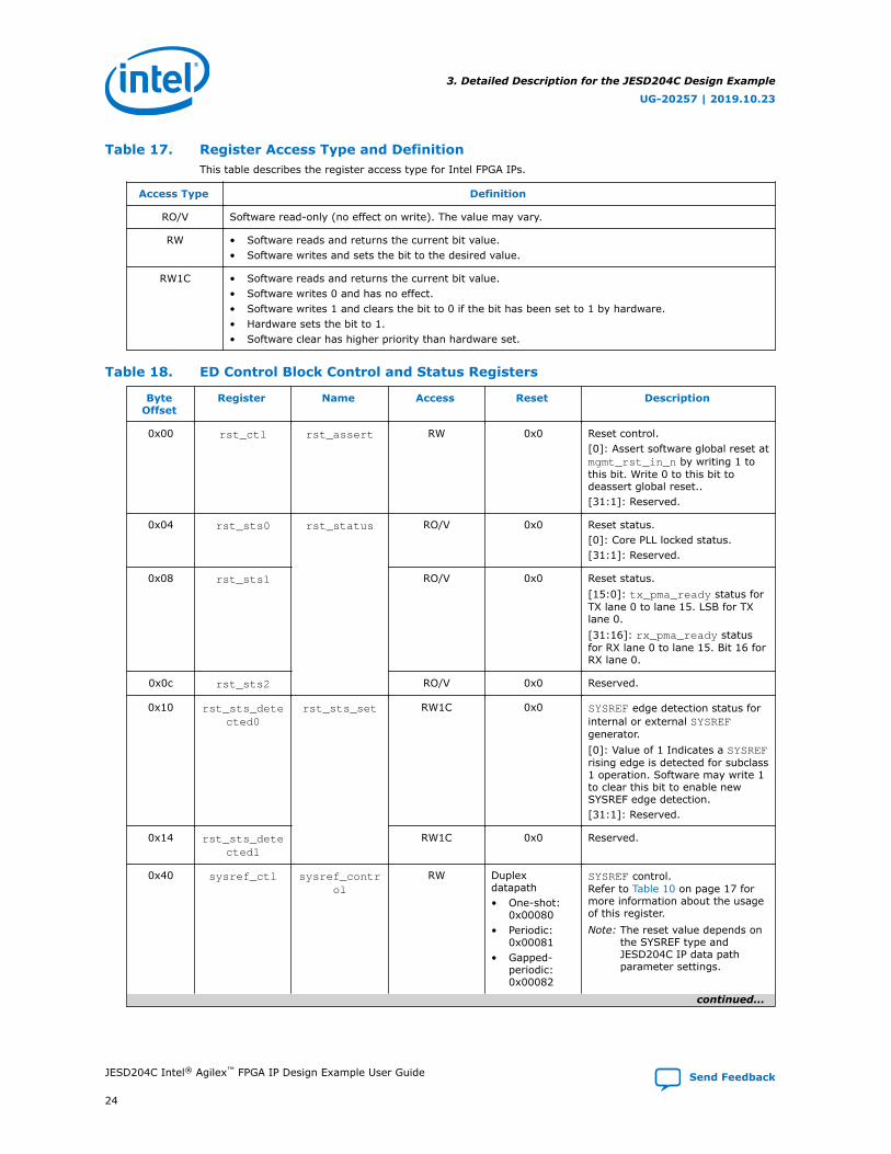
Table 17. Register Access Type and DefinitionThis table describes the register access type for Intel FPGA IPs.
Access Type Definition
RO/V Software read-only (no effect on write). The value may vary.
RW • Software reads and returns the current bit value.• Software writes and sets the bit to the desired value.
RW1C • Software reads and returns the current bit value.• Software writes 0 and has no effect.• Software writes 1 and clears the bit to 0 if the bit has been set to 1 by hardware.• Hardware sets the bit to 1.• Software clear has higher priority than hardware set.
Table 18. ED Control Block Control and Status Registers
ByteOffset
Register Name Access Reset Description
0x00 rst_ctl rst_assert RW 0x0 Reset control.[0]: Assert software global reset atmgmt_rst_in_n by writing 1 tothis bit. Write 0 to this bit todeassert global reset..[31:1]: Reserved.
0x04 rst_sts0 rst_status RO/V 0x0 Reset status.[0]: Core PLL locked status.[31:1]: Reserved.
0x08 rst_sts1 RO/V 0x0 Reset status.[15:0]: tx_pma_ready status forTX lane 0 to lane 15. LSB for TXlane 0.[31:16]: rx_pma_ready statusfor RX lane 0 to lane 15. Bit 16 forRX lane 0.
0x0c rst_sts2 RO/V 0x0 Reserved.
0x10 rst_sts_detected0
rst_sts_set RW1C 0x0 SYSREF edge detection status forinternal or external SYSREFgenerator.[0]: Value of 1 Indicates a SYSREFrising edge is detected for subclass1 operation. Software may write 1to clear this bit to enable newSYSREF edge detection.[31:1]: Reserved.
0x14 rst_sts_detected1
RW1C 0x0 Reserved.
0x40 sysref_ctl sysref_control
RW Duplexdatapath• One-shot:
0x00080• Periodic:
0x00081• Gapped-
periodic:0x00082
SYSREF control.Refer to Table 10 on page 17 formore information about the usageof this register.Note: The reset value depends on
the SYSREF type andJESD204C IP data pathparameter settings.
continued...
3. Detailed Description for the JESD204C Design Example
UG-20257 | 2019.10.23
JESD204C Intel® Agilex™ FPGA IP Design Example User Guide Send Feedback
24

ByteOffset
Register Name Access Reset Description
TX or RX datapath• One-shot:
0x00000• Periodic:
0x00001• Gapped-
periodic:0x00002
0x44 sysref_sts sysref_status
RO/V 0x0 SYSREF status. This registercontains the latest SYSREF periodand duty cycle settings of theinternal SYSREF generator.Refer to Table 9 on page 17 for thelegal value of the SYSREF periodand duty cycle.[7:0]: SYSREF period.• When the value is 0xFF, the
SYSREF period = 255.• When the value if 0x00, the
SYSREF period = 256.[15:8]: SYSREF duty cycle.[31:16]: Reserved.
0x80 tst_ctl tst_control RW 0x0 Test control. Use this register toenable different test patterns forthe pattern generator and checker.[1:0] = prbs_test_ctl• 2’b00 = PRBS23• 2’b01 = PRBS15• 2’b10 = PRBS9• 2’b11 = PRBS7[2] = ramp_test_ctl• 1’b0 = Enable PRBS pattern• 1’b1 = Enable ramp pattern[31:3]: Reserved.
0x84 tst_sts0 tst_status RW1C 0x0 Reserved.
0x88 tst_sts1 RW1C 0x0 Reserved.
0x8c tst_err0 tst_error RW1C 0x0 Error flag for Link 0. When the bitis 1’b1, it indicates an error hashappened. You should resolve theerror before writing 1’b1 to therespective bit to clear the errorflag.[0] = Pattern checker error[1] = tx_link_error[2] = rx_link_error[3] = Command pattern checkererror[31:4]: Reserved.
0x90 tst_err1 RW1C 0x0 Reserved.
3. Detailed Description for the JESD204C Design Example
UG-20257 | 2019.10.23
Send Feedback JESD204C Intel® Agilex™ FPGA IP Design Example User Guide
25

4. Document Revision History for the JESD204C IntelAgilex FPGA IP Design Example User Guide
Document Version Intel QuartusPrime Version
IP Version Changes
2019.10.23 19.3 1.0.0 Initial release.
UG-20257 | 2019.10.23
Send Feedback
Intel Corporation. All rights reserved. Agilex, Altera, Arria, Cyclone, Enpirion, Intel, the Intel logo, MAX, Nios,Quartus and Stratix words and logos are trademarks of Intel Corporation or its subsidiaries in the U.S. and/orother countries. Intel warrants performance of its FPGA and semiconductor products to current specifications inaccordance with Intel's standard warranty, but reserves the right to make changes to any products and servicesat any time without notice. Intel assumes no responsibility or liability arising out of the application or use of anyinformation, product, or service described herein except as expressly agreed to in writing by Intel. Intelcustomers are advised to obtain the latest version of device specifications before relying on any publishedinformation and before placing orders for products or services.*Other names and brands may be claimed as the property of others.
ISO9001:2015Registered