Jan M. Rabaey Anantha Chandrakasan Borivoje Nikolic Design ...baccaran/Rabaey/chapter08.pdf · ©...
60
© Digital Integrated Circuits 2nd Design Methodologies Digital Integrated Digital Integrated Circuits Circuits A Design Perspective A Design Perspective Design Design Methodologies Methodologies Jan M. Rabaey Anantha Chandrakasan Borivoje Nikolic December 10, 2002
Transcript of Jan M. Rabaey Anantha Chandrakasan Borivoje Nikolic Design ...baccaran/Rabaey/chapter08.pdf · ©...

© Digital Integrated Circuits2nd Design Methodologies
Digital Integrated Digital Integrated CircuitsCircuitsA Design PerspectiveA Design Perspective
DesignDesignMethodologiesMethodologies
Jan M. RabaeyAnantha ChandrakasanBorivoje Nikolic
December 10, 2002
© Digital Integrated Circuits2nd Design Methodologies
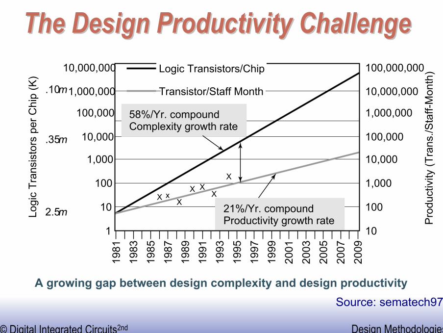
The Design Productivity ChallengeThe Design Productivity Challenge
Source: sematech97A growing gap between design complexity and design productivity
1 9 8 1
L o g i c T r a n s i s t o r s p e r C h i p ( K )
P r o d u c t i v i t y ( T r a n s . / S t a f f - M o n t h )
1 9 8 3 1 9 8 5 1 9 8 7 1 9 8 9 1 9 9 1 1 9 9 3 1 9 9 5 1 9 9 7 1 9 9 9 2 0 0 1 2 0 0 3 2 0 0 5 2 0 0 7 2 0 0 9
58%/Yr. compoundComplexity growth rate
21%/Yr. compoundProductivity growth rate
1981
10Logi
c Tr
ansi
stor
s pe
r Chi
p (K
)
Pro
duct
ivity
(Tra
ns./S
taff-
Mon
th)
100
1,000
10,000
100,000
1,000,000
10,000,000
1
X XX X
X
X
x100
1,000
10,000
100,000
1,000,000
10,000,000
100,000,000
10
2.5m
.35m
.10m
1983
1985
1987
1989
1991
1993
1995
1997
1999
2001
2003
2005
2007
2009
Transistor/Staff Month
Logic Transistors/Chip

© Digital Integrated Circuits2nd Design Methodologies
A Simple ProcessorA Simple Processor
MEMORY
DATAPATH
CONTROL
I N P U T - O U T P U T
INP
UT/
OU
TPU
T

© Digital Integrated Circuits2nd Design Methodologies
A SystemA System--onon--aa--Chip: ExampleChip: Example
Courtesy: Philips
© Digital Integrated Circuits2nd Design Methodologies
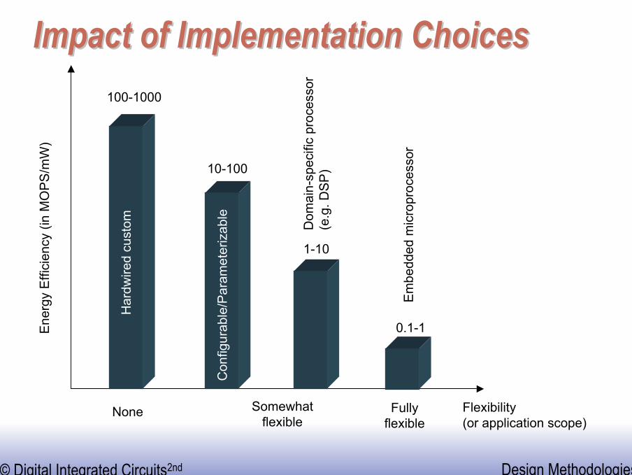
Impact of Implementation ChoicesImpact of Implementation ChoicesE
nerg
y E
ffici
ency
(in
MO
PS
/mW
)
Flexibility(or application scope)
0.1-1
1-10
10-100
100-1000
None Fullyflexible
Somewhatflexible
Har
dwire
d cu
stom
Con
figur
able
/Par
amet
eriz
able
Dom
ain-
spec
ific
proc
esso
r(e
.g. D
SP
)
Em
bedd
ed m
icro
proc
esso
r

© Digital Integrated Circuits2nd Design Methodologies
Design MethodologyDesign Methodology
• Design process traverses iteratively between three abstractions:behavior, structure, and geometry
• More and more automation for each of these steps
© Digital Integrated Circuits2nd Design Methodologies
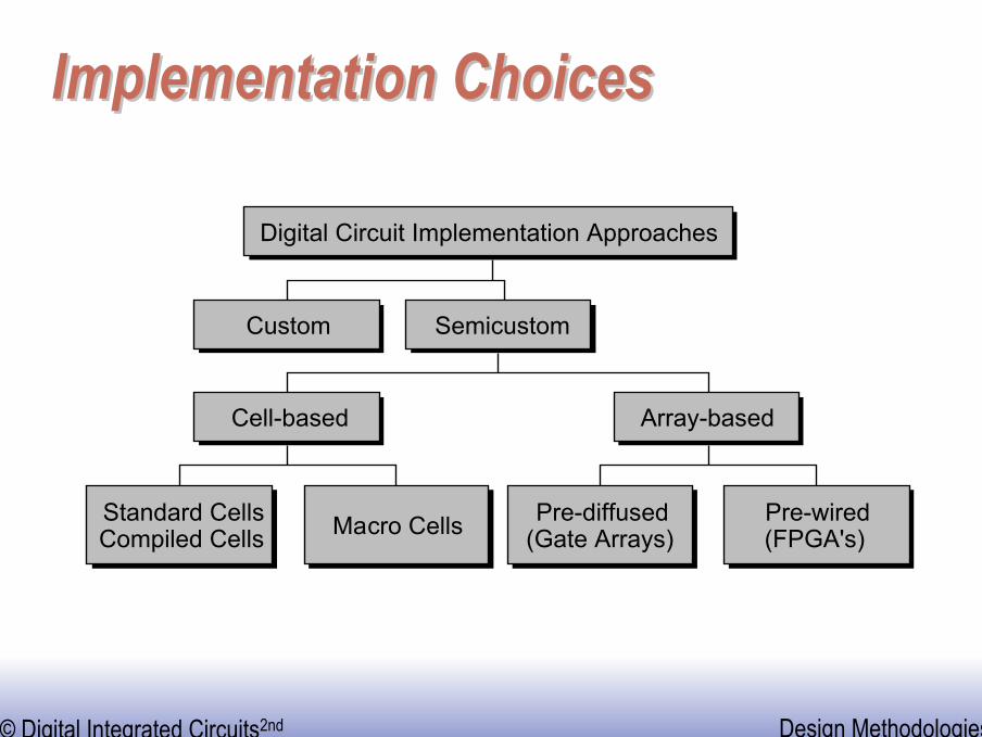
Implementation ChoicesImplementation Choices
Custom
Standard CellsCompiled Cells Macro Cells
Cell-based
Pre-diffused(Gate Arrays)
Pre-wired(FPGA's)
Array-based
Semicustom
Digital Circuit Implementation Approaches
© Digital Integrated Circuits2nd Design Methodologies
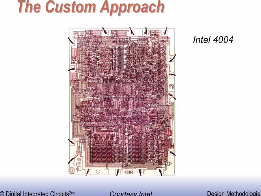
The Custom Approach The Custom Approach
Intel 4004
Courtesy Intel

© Digital Integrated Circuits2nd Design Methodologies
Transition to Automation and Regular StructuresTransition to Automation and Regular Structures
Intel 4004 (‘71)Intel 4004 (‘71)Intel 8080Intel 8080 Intel 8085Intel 8085
Intel 8286Intel 8286 Intel 8486Intel 8486Courtesy Intel

© Digital Integrated Circuits2nd Design Methodologies
CellCell--based Design (or standard cells)based Design (or standard cells)
Routing channel requirements arereduced by presenceof more interconnectlayers
Functionalmodule(RAM,multiplier, …)
Routingchannel
Logic cellFeedthrough cellR
ows
of c
ells
© Digital Integrated Circuits2nd Design Methodologies
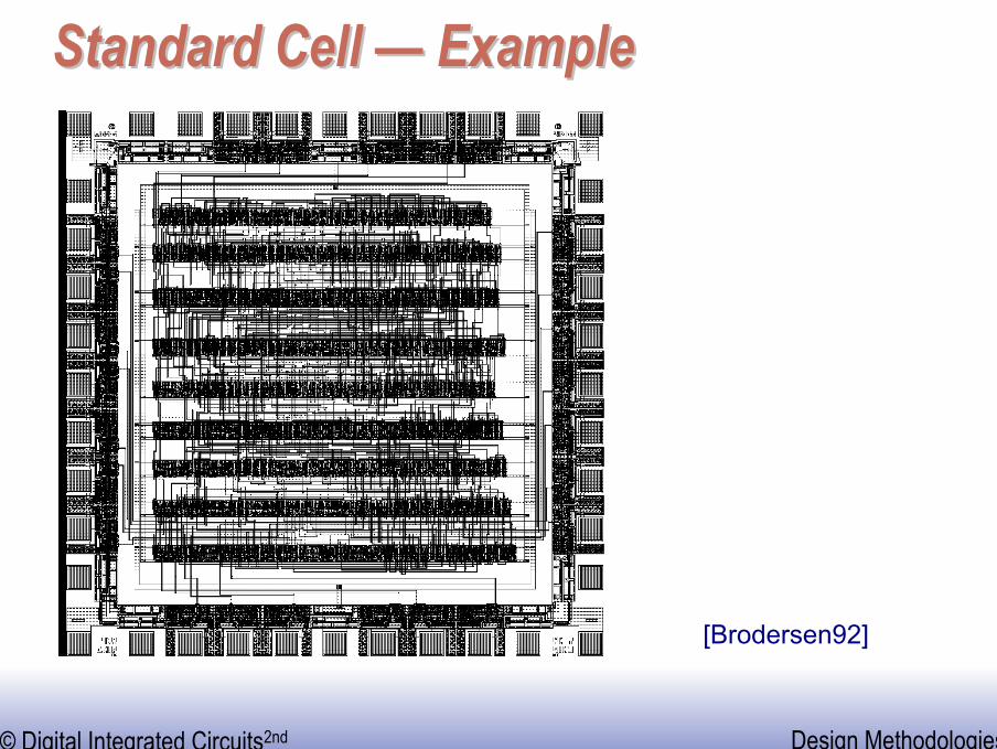
Standard Cell Standard Cell —— ExampleExample
[Brodersen92]

© Digital Integrated Circuits2nd Design Methodologies
Standard Cell Standard Cell –– The New GenerationThe New Generation
Cell-structurehidden underinterconnect layers
© Digital Integrated Circuits2nd Design Methodologies
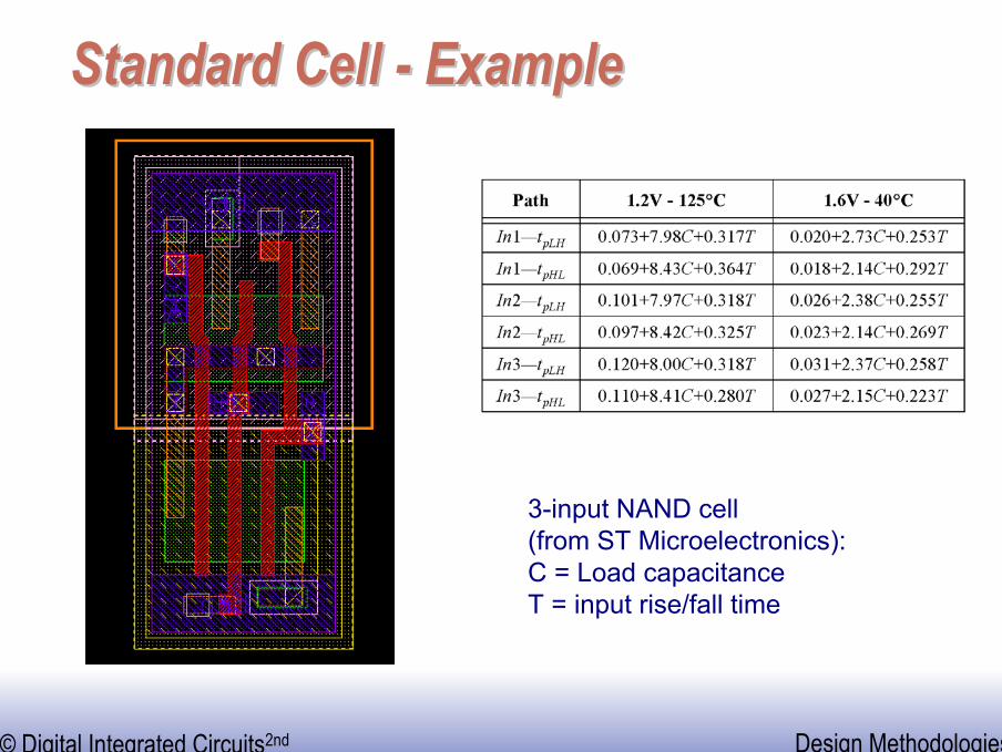
Standard Cell Standard Cell -- ExampleExample
3-input NAND cell(from ST Microelectronics):C = Load capacitanceT = input rise/fall time
© Digital Integrated Circuits2nd Design Methodologies
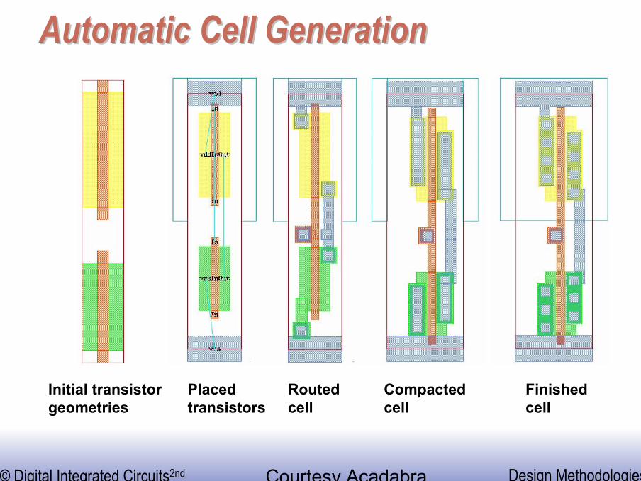
Automatic Cell GenerationAutomatic Cell Generation
Courtesy Acadabra
Initial transistorgeometries
Placedtransistors
Routedcell
Compactedcell
Finishedcell

© Digital Integrated Circuits2nd Design Methodologies
A Historical Perspective: the PLAA Historical Perspective: the PLA
x0 x1 x2
ANDplane
x0x1
x2
Product terms
ORplane
f0 f1

© Digital Integrated Circuits2nd Design Methodologies
TwoTwo--Level LogicLevel Logic
Inverting format (NOR-NOR) more effective
Every logic function can beexpressed in sum-of-productsformat (AND-OR)
minterm

© Digital Integrated Circuits2nd Design Methodologies
PLA Layout PLA Layout –– Exploiting RegularityExploiting Regularity
f0 f1x0 x0 x1 x1 x2 x2
Pull-up devices Pull-up devices
VDD GNDφAnd-Plane Or-Plane

© Digital Integrated Circuits2nd Design Methodologies
Breathing Some New Life in Breathing Some New Life in PLAsPLAsRiver PLAs
A cascade of multiple-output PLAs.Adjacent PLAs are connected via river routing.
PRE-CHARGE
PRE-
CH
AR
GE
PRE-CHARGE
PRE-
CH
AR
GE
BUFFER
BUFFER
BU
FFER
BU
FFER
PRE-CHARGE
PRE-
CH
AR
GE
BUFFER
BU
FFER
PRE-CHARGE
PRE-
CH
AR
GE
BUFFERB
UFF
ER
• No placement and routing needed. • Output buffers and the input buffers
of the next stage are shared.
Courtesy B. Brayton
© Digital Integrated Circuits2nd Design Methodologies
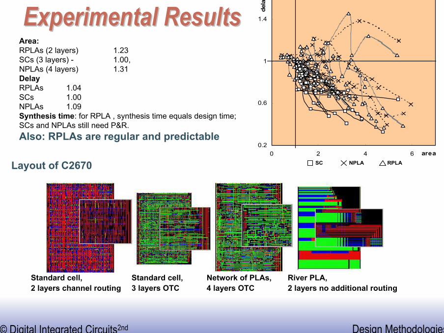
Experimental ResultsExperimental Results
Layout of C2670
Network of PLAs, 4 layers OTC
River PLA,2 layers no additional routing
Standard cell, 2 layers channel routing
Standard cell,3 layers OTC
0.2
0.6
1
1.4
0 2 4 6 area
dela
y
SC NPLA RPLA
Area: RPLAs (2 layers) 1.23 SCs (3 layers) - 1.00, NPLAs (4 layers) 1.31 DelayRPLAs 1.04SCs 1.00 NPLAs 1.09 Synthesis time: for RPLA , synthesis time equals design time; SCs and NPLAs still need P&R.Also: RPLAs are regular and predictable

© Digital Integrated Circuits2nd Design Methodologies
MacroModulesMacroModules
256×32 (or 8192 bit) SRAMGenerated by hard-macro module generator
© Digital Integrated Circuits2nd Design Methodologies
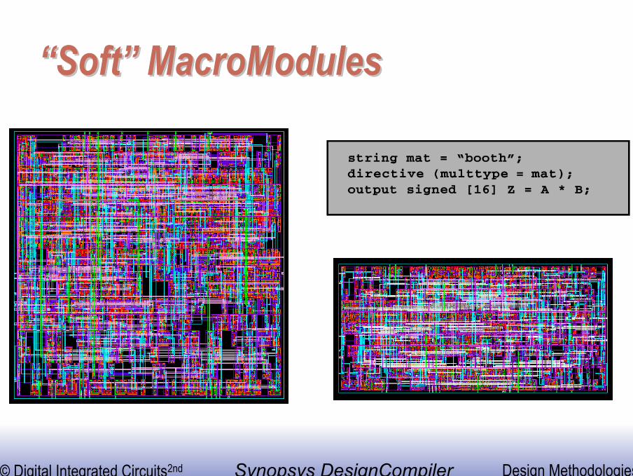
“Soft” “Soft” MacroModulesMacroModules
Synopsys DesignCompiler

© Digital Integrated Circuits2nd Design Methodologies
“Intellectual Property”“Intellectual Property”
A Protocol Processor for Wireless

© Digital Integrated Circuits2nd Design Methodologies
SemicustomSemicustom Design FlowDesign Flow
HDLHDL
Logic SynthesisLogic Synthesis
FloorplanningFloorplanning
PlacementPlacement
RoutingRouting
Tape-out
Circuit ExtractionCircuit Extraction
Pre-Layout Simulation
Pre-Layout Simulation
Post-Layout Simulation
Post-Layout Simulation
StructuralStructural
PhysicalPhysical
BehavioralBehavioralDesign Capture
Des
ign
Itera
tion
Des
ign
Itera
tion

© Digital Integrated Circuits2nd Design Methodologies
The “Design Closure” ProblemThe “Design Closure” Problem
Courtesy Synopsys
Iterative Removal of Timing Violations (white lines)

© Digital Integrated Circuits2nd Design Methodologies
Integrating Synthesis with Integrating Synthesis with Physical DesignPhysical Design
Physical SynthesisPhysical Synthesis
RTL (Timing) Constraints
Place-and-RouteOptimization
Place-and-RouteOptimization
Artwork
Netlist with Place-and-Route Info
MacromodulesFixed netlists
© Digital Integrated Circuits2nd Design Methodologies
Pre-diffused(Gate Arrays)
Pre-wired(FPGA's)
Array-based
LateLate--Binding ImplementationBinding Implementation

© Digital Integrated Circuits2nd Design Methodologies
Gate Array Gate Array —— SeaSea--ofof--gatesgates
rows of
cells
routing channel
uncommitted
VDD
GND
polysilicon
metal
possiblecontact
In1 In2 In3 In4
Out
UncommitedCell
CommittedCell(4-input NOR)

© Digital Integrated Circuits2nd Design Methodologies
SeaSea--ofof--gate Primitive Cellsgate Primitive Cells
NMOS
PMOS
Oxide-isolation
PMOS
NMOS
NMOS
Using oxide-isolation Using gate-isolation
© Digital Integrated Circuits2nd Design Methodologies
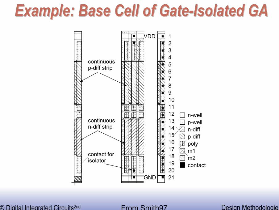
Example: Base Cell of GateExample: Base Cell of Gate--Isolated GAIsolated GA
n-well
contact
21GND2019181716151413121110987654321VDD
m2m1polyp-diffn-diffp-well
contact forisolator
continuousn-diff strip
continuousp-diff strip
From Smith97

© Digital Integrated Circuits2nd Design Methodologies
Example: FlipExample: Flip--Flop in GateFlop in Gate--Isolated GAIsolated GA
CLK
D
Q
GND
VDD
Q
CLR
From Smith97
© Digital Integrated Circuits2nd Design Methodologies
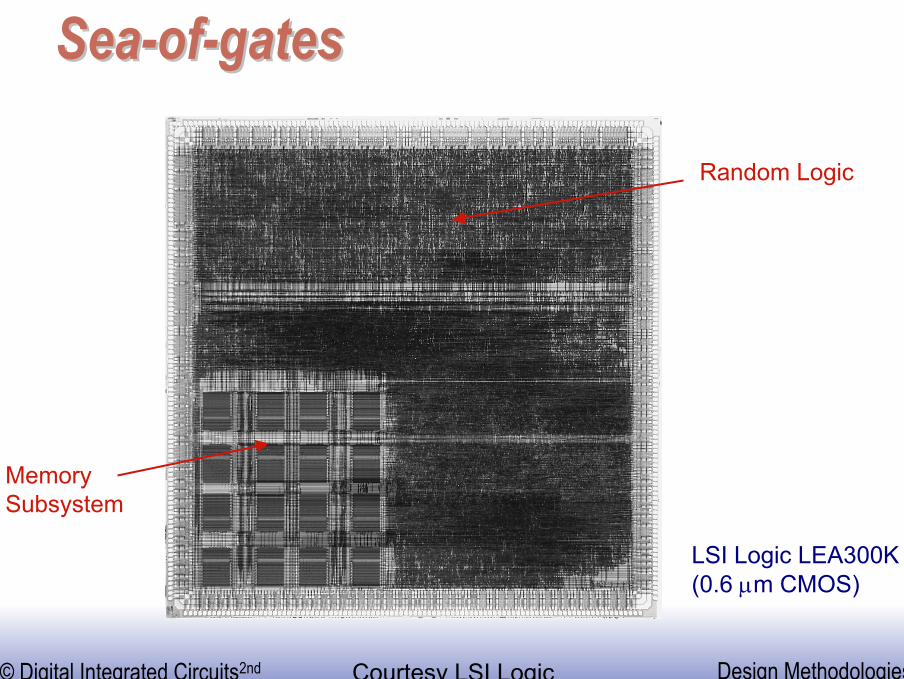
SeaSea--ofof--gatesgates
Random Logic
MemorySubsystem
LSI Logic LEA300K(0.6 µm CMOS)
Courtesy LSI Logic

© Digital Integrated Circuits2nd Design Methodologies
The return of gate arrays?The return of gate arrays?
metal-5 metal-6
Via-programmable cross-point
programmable via
Via programmable gate array(VPGA)
[Pileggi02]
Exploits regularity of interconnect
© Digital Integrated Circuits2nd Design Methodologies
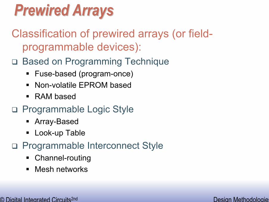
PrewiredPrewired ArraysArraysClassification of prewired arrays (or field-
programmable devices):Based on Programming Technique
Fuse-based (program-once)Non-volatile EPROM basedRAM based
Programmable Logic StyleArray-BasedLook-up Table
Programmable Interconnect StyleChannel-routingMesh networks

© Digital Integrated Circuits2nd Design Methodologies
FuseFuse--Based FPGABased FPGA
antifuse polysilicon ONO dielectric
n+ antifuse diffusion
2 l
From Smith97
Open by default, closed by applying current pulse

© Digital Integrated Circuits2nd Design Methodologies
ArrayArray--Based Programmable LogicBased Programmable Logic
PLA PROM PAL
I5 I4
O0
I3 I2 I1 I0
O1O2O3
Programmable AND array
ProgrammableOR array I5 I4
O0
I3 I2 I1 I0
O1O2O3
Programmable AND array
Fixed OR array
Indicates programmable connection
Indicates fixed connection
O0
I3 I2 I1 I0
O1O2O3
Fixed AND array
ProgrammableOR array
© Digital Integrated Circuits2nd Design Methodologies
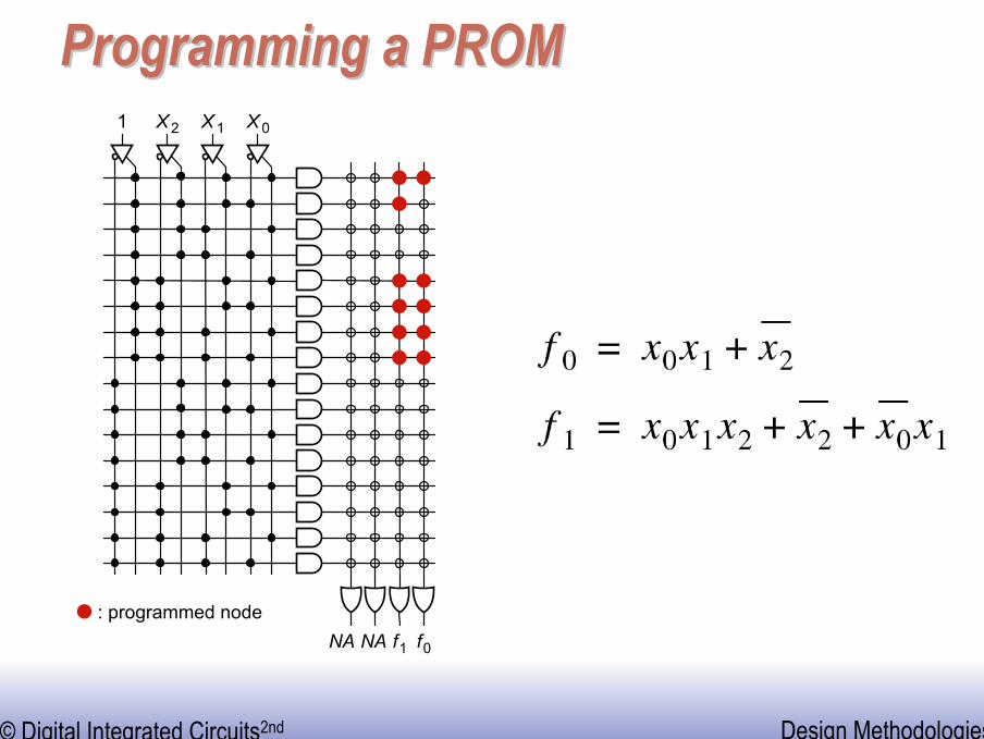
Programming a PROMProgramming a PROM
f0
1 X 2 X 1 X 0
f1NANA: programmed node

© Digital Integrated Circuits2nd Design Methodologies
More Complex PALMore Complex PAL
From Smith97
programmable AND array (2 i 3 jk ) k macrocells
j -wide OR array
j
macrocell
productterms
D Q
A
1
j
BCLK
OUT
C i i inputs
i inputs, j minterms/macrocell, k macrocells

© Digital Integrated Circuits2nd Design Methodologies
22--input input muxmuxas programmable logic blockas programmable logic block
FA 0
B
S
1
ConfigurationA B S F=0 0 0 00 X 1 X0 Y 1 Y0 Y X XYX 0 YY 0 XY 1 X X 1 Y1 0 X1 0 Y1 1 1 1
XYXY
XY
© Digital Integrated Circuits2nd Design Methodologies
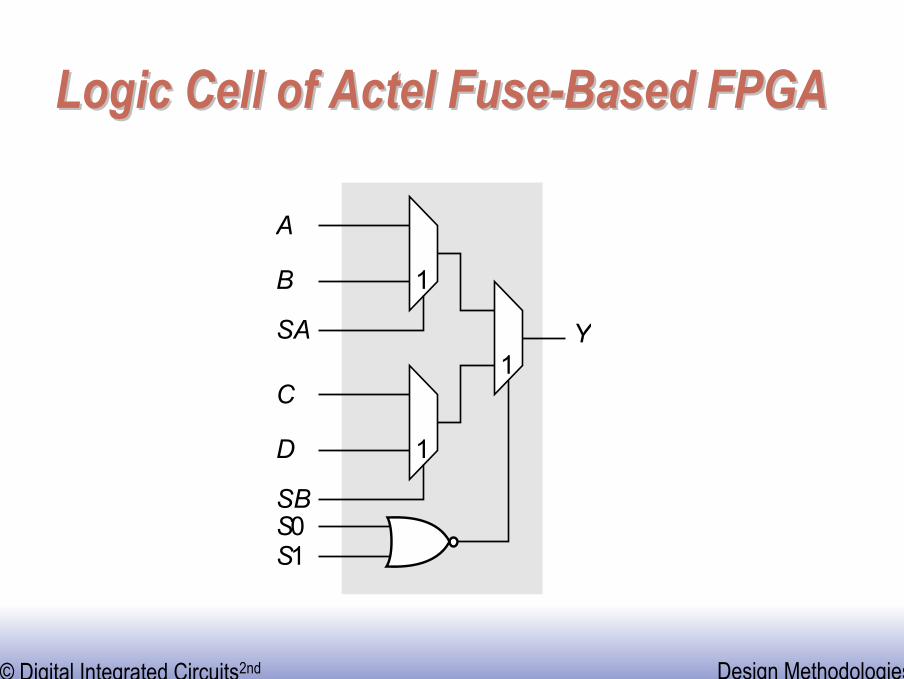
Logic Cell of Logic Cell of ActelActel FuseFuse--Based FPGABased FPGA
A
B
SA Y
1
C
D
SB
1
S0S1
1

© Digital Integrated Circuits2nd Design Methodologies
LookLook--up Table Based Logic Cellup Table Based Logic Cell
Out
ln1 ln2
Mem
ory In Out
00 00
01 1
10 1
11 0

© Digital Integrated Circuits2nd Design Methodologies
LUTLUT--Based Logic CellBased Logic Cell
Courtesy Xilinx
D4
C1....C4
xxxxxx
D3
D2
D1
F4
F3
F2
F1
Logicfunction
ofxxx
Logicfunction
ofxxx
Logicfunction
ofxxx
xx
xx
4
xxxxxx
xxxxxxxx
xxx
xxxx xxxx xxxx
HP
Bitscontrol
Bitscontrol
Multiplexer Controlledby Configuration Program
x
xx
x
xx
xxx xx
xxxx
x
xxxxxx
xx
x
xx
xxx
xx
Xilinx 4000 Series
Figure must be updated
© Digital Integrated Circuits2nd Design Methodologies
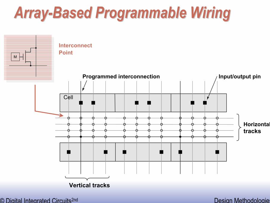
ArrayArray--Based Programmable WiringBased Programmable Wiring
Input/output pinProgrammed interconnection
InterconnectPoint
Horizontaltracks
Vertical tracks
Cell
M
© Digital Integrated Circuits2nd Design Methodologies
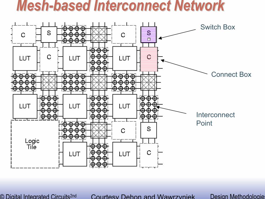
MeshMesh--based Interconnect Networkbased Interconnect NetworkSwitch Box
Connect Box
InterconnectPoint
Courtesy Dehon and Wawrzyniek

© Digital Integrated Circuits2nd Design Methodologies
Transistor Implementation of MeshTransistor Implementation of Mesh
Courtesy Dehon and Wawrzyniek
© Digital Integrated Circuits2nd Design Methodologies
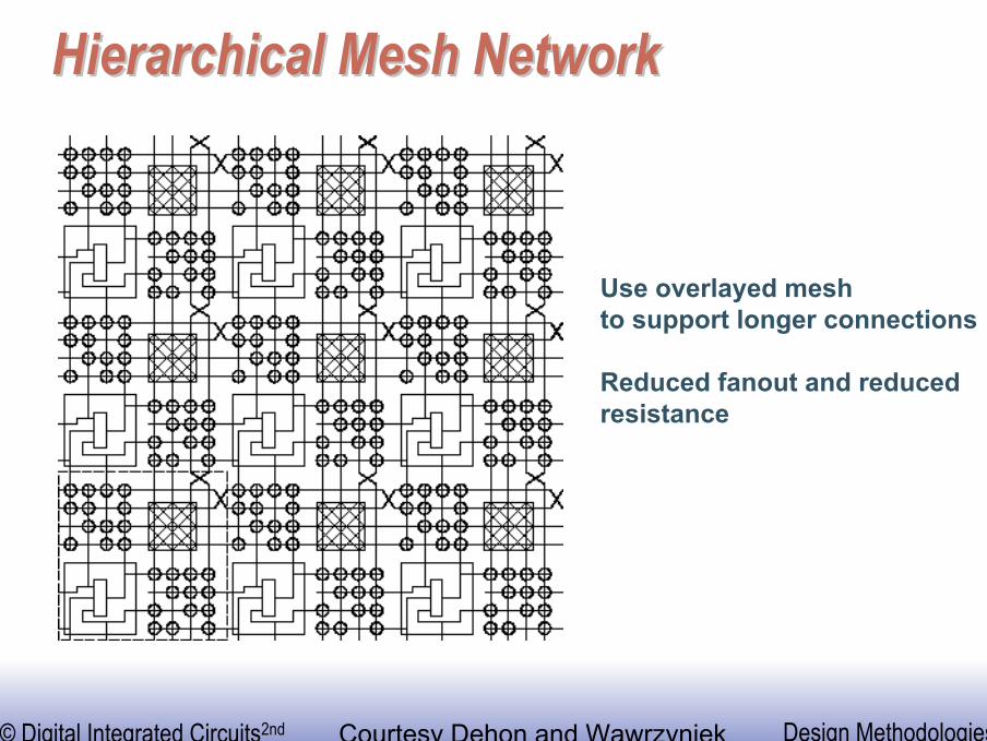
Hierarchical Mesh NetworkHierarchical Mesh Network
Use overlayed meshto support longer connections
Reduced fanout and reduced resistance
Courtesy Dehon and Wawrzyniek
© Digital Integrated Circuits2nd Design Methodologies
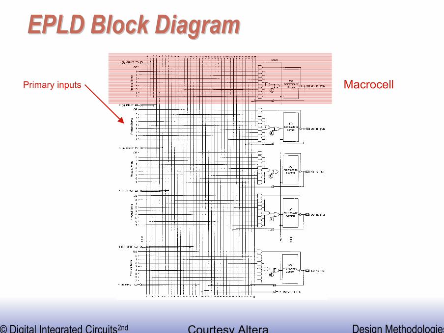
EPLD Block DiagramEPLD Block Diagram
MacrocellPrimary inputs
Courtesy Altera

© Digital Integrated Circuits2nd Design Methodologies
AlteraAltera MAXMAX
From Smith97

© Digital Integrated Circuits2nd Design Methodologies
AlteraAltera MAX Interconnect ArchitectureMAX Interconnect Architecture
LAB2
PIA
LAB1
LAB6
tPIA
tPIA
row channelcolumn channel
LAB
Courtesy Altera
Array-based(MAX 3000-7000)
Mesh-based(MAX 9000)

© Digital Integrated Circuits2nd Design Methodologies
FieldField--Programmable Gate ArraysProgrammable Gate ArraysFuseFuse--basedbased
I/O Buffers
Program/Test/Diagnostics
I/O Buffers
I/O B
uffe
rs
I/O B
uffe
rs
Vertical routes
Rows of logic modulesRouting channels
Standard-cell likefloorplan
© Digital Integrated Circuits2nd Design Methodologies
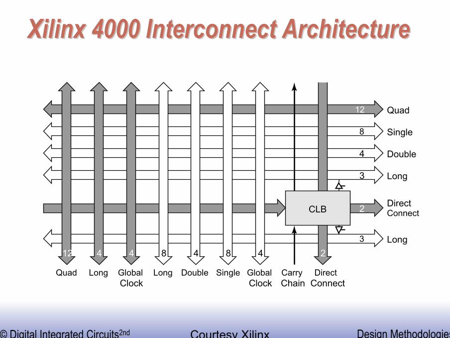
Xilinx 4000 Interconnect ArchitectureXilinx 4000 Interconnect Architecture
2
12
8
4
3
2
3
CLB
8 4 8 4
Quad
Single
Double
Long
DirectConnect
DirectConnect
Quad Long GlobalClock
Long Double Single GlobalClock
CarryChain
Long12 4 4
Courtesy Xilinx

© Digital Integrated Circuits2nd Design Methodologies
RAMRAM--based FPGA based FPGA
Xilinx XC4000ex
Courtesy Xilinx

© Digital Integrated Circuits2nd Design Methodologies
A LowA Low--Energy FPGA (UC Berkeley)Energy FPGA (UC Berkeley)
Array Size: 8x8 (2 x 4 LUT)Power Supply: 1.5V & 0.8VConfiguration: Mapped as RAMToggle Frequency:125MHzArea: 3mm x 3mm
© Digital Integrated Circuits2nd Design Methodologies
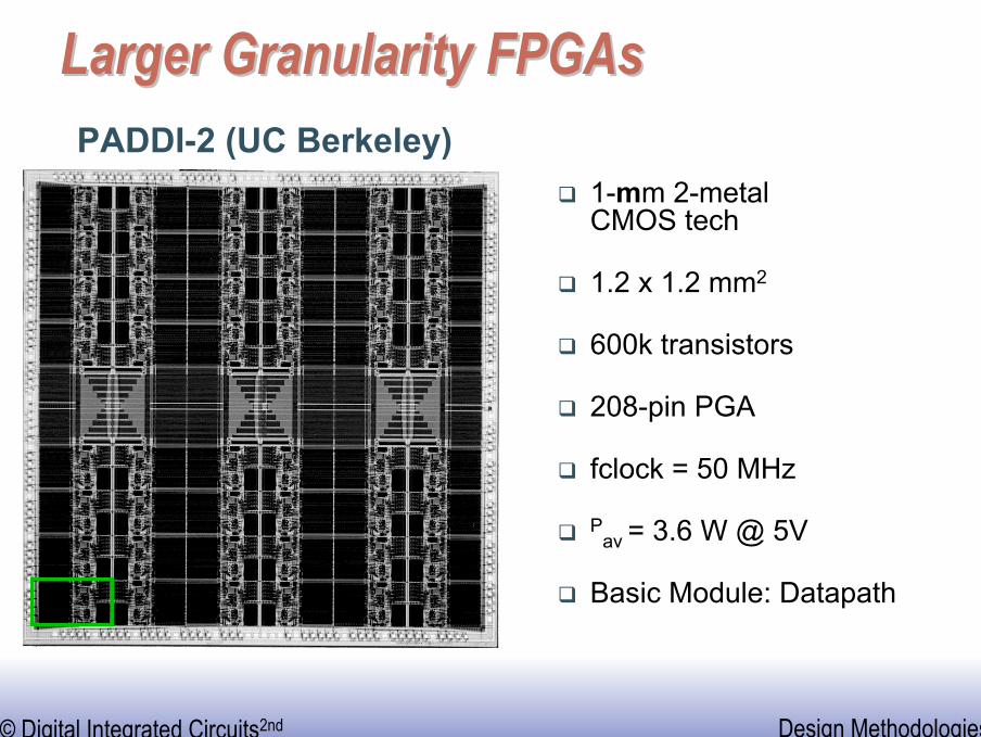
Larger Granularity Larger Granularity FPGAsFPGAs
1-mm 2-metalCMOS tech
1.2 x 1.2 mm2
600k transistors
208-pin PGA
fclock = 50 MHz
Pav = 3.6 W @ 5V
Basic Module: Datapath
PADDI-2 (UC Berkeley)

© Digital Integrated Circuits2nd Design Methodologies
Design at a crossroadDesign at a crossroadSystemSystem--onon--aa--ChipChip
RAM
500 k Gates FPGA+ 1 Gbit DRAMPreprocessing
Multi-SpectralImager
µCsystem+2 GbitDRAMRecog-nition
Ana
log
64 SIMD ProcessorArray + SRAM
Image Conditioning100 GOPS
Embedded applications where cost, performance, and energy are the real issues!DSP and control intensiveMixed-modeCombines programmable and application-specific modulesSoftware plays crucial role
© Digital Integrated Circuits2nd Design Methodologies
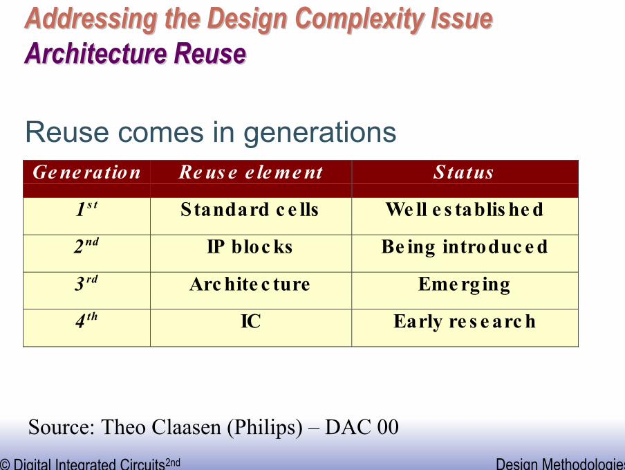
Addressing the Design Complexity IssueAddressing the Design Complexity IssueArchitecture ReuseArchitecture Reuse
Reuse comes in generationsGe ne ration Re us e e le me nt Status
1s t Standard c e lls We ll e s tablis he d
2nd IP bloc ks Be ing introduc e d
3rd Arc hite c ture Eme rg ing
4th IC Early re s e arc h
Source: Theo Claasen (Philips) – DAC 00

© Digital Integrated Circuits2nd Design Methodologies
Architecture Architecture ReUseReUseSilicon System Platform
Flexible architecture for hardware and softwareSpecific (programmable) componentsNetwork architectureSoftware modulesRules and guidelines for design of HW and SW
Has been successful in PC’sDominance of a few players who specify and control architecture
Application-domain specific (difference in constraints)Speed (compute power)DissipationCostsReal / non-real time data

© Digital Integrated Circuits2nd Design Methodologies
PlatformPlatform--Based DesignBased Design
A platform is a restriction on the space of possible implementation choices, providing a well-defined abstraction of the underlying technology for the application developerNew platforms will be defined at the architecture-micro-architecture boundaryThey will be component-based, and will provide a range of choices from structured-custom to fully programmable implementationsKey to such approaches is the representation of communication in the platform model
“Only the consumer gets freedom of choice;“Only the consumer gets freedom of choice;designers need freedomdesigners need freedom fromfrom choice”choice”
((OrfaliOrfali, et al, 1996, p.522), et al, 1996, p.522)
Source:R.Newton

© Digital Integrated Circuits2nd Design Methodologies
Berkeley Pleiades ProcessorBerkeley Pleiades Processor
• 0.25um 6-level metal CMOS
• 5.2mm x 6.7mm
• 1.2 Million transistors
• 40 MHz at 1V
• 2 extra supplies: 0.4V, 1.5V
• 1.5~2 mW power dissipationInterface
Reconfigurable
Data-path
FPGA
ARM8 Core

© Digital Integrated Circuits2nd Design Methodologies
Heterogeneous Programmable PlatformsHeterogeneous Programmable Platforms
Xilinx Vertex-II Pro
Courtesy Xilinx
High-speed I/O
Embedded PowerPcEmbedded memories
Hardwired multipliers
FPGA Fabric

© Digital Integrated Circuits2nd Design Methodologies
SummarySummary
Digital CMOS Design is kicking and healthySome major challenges down the road caused by Deep Sub-micron
Super GHz designPower consumption!!!!Reliability – making it work
Some new circuit solutions are bound to emergeWho can afford design in the years to come? Some major design methodology change in the making!
![[Jan M. Rabaey, Massoud Pedram] Low-Power-Design-M(Bookos.org)](https://static.fdocuments.in/doc/165x107/55cf9cda550346d033ab4ad0/jan-m-rabaey-massoud-pedram-low-power-design-mbookosorg.jpg)