Digital Integrated Circuits© Prentice Hall 1995 Devices Jan M. Rabaey The Devices.
67
Digital Integrated Circuits © Prentice Hall 1995 Devices Devices Jan M. Rabaey The Devices
-
Upload
charleen-french -
Category
Documents
-
view
229 -
download
1
Transcript of Digital Integrated Circuits© Prentice Hall 1995 Devices Jan M. Rabaey The Devices.
Digital Integrated Circuits © Prentice Hall 1995DevicesDevices
Jan M. Rabaey
The Devices

Digital Integrated Circuits © Prentice Hall 1995DevicesDevices
Goal of this chapter
• Present intuitive understanding of device operation
• Introduction of basic device equations
• Introduction of models for manual analysis
• Introduction of models for SPICE simulation
• Analysis of secondary and deep-sub-microneffects
• Future trends

Digital Integrated Circuits © Prentice Hall 1995DevicesDevices
The Diode
n
p
p
n
B A SiO2Al
A
B
Al
A
B
Cross-section of pn-junction in an IC process
One-dimensionalrepresentation diode symbol

Digital Integrated Circuits © Prentice Hall 1995DevicesDevices
Depletion Region
hole diffusionelectron diffusion
p n
hole driftelectron drift
ChargeDensity
Distancex+
-
ElectricalxField
x
PotentialV
W2-W1
(a) Current flow.
(b) Charge density.
(c) Electric field.
(d) Electrostaticpotential.

Digital Integrated Circuits © Prentice Hall 1995DevicesDevices
Diode Current

Digital Integrated Circuits © Prentice Hall 1995DevicesDevices
Forward Bias
x
pn0
np0
-W1 W20
p n(W
2)
n-regionp-region
Lp
diffusion

Digital Integrated Circuits © Prentice Hall 1995DevicesDevices
Reverse Bias
x
pn0
np0
-W1 W20n-regionp-region
diffusion

Digital Integrated Circuits © Prentice Hall 1995DevicesDevices
Diode Types
x
x
pn0
pn0
Wn
pn(x)
pn(x)
Wn
Short-base Diode
Long-base Diode
(standard in semiconductordevices)

Digital Integrated Circuits © Prentice Hall 1995DevicesDevices
Models for Manual Analysis
VD
ID = IS(eVD/T – 1)+
–
VD
+
–
+
–VDon
ID
(a) Ideal diode model (b) First-order diode model
Digital Integrated Circuits © Prentice Hall 1995DevicesDevices
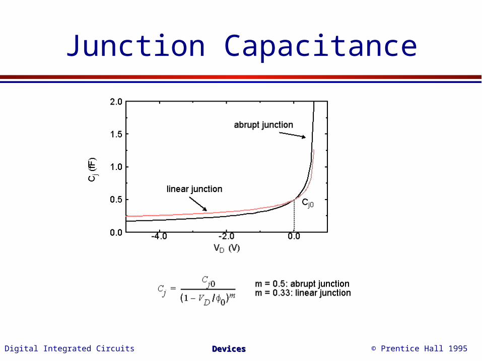
Junction Capacitance

Digital Integrated Circuits © Prentice Hall 1995DevicesDevices
Diffusion Capacitance

Digital Integrated Circuits © Prentice Hall 1995DevicesDevices
Diode Switching Time
Vsrc
t = 0
V1
V2
VD
Rsrc
t = T
ID
Time
VD
ON OFF ON
Space chargeExcess charge

Digital Integrated Circuits © Prentice Hall 1995DevicesDevices
Secondary Effects
–25.0 –15.0 –5.0 5.0
VD (V)
–0.1
I D (A
)0.1
0
0
Avalanche Breakdown
Digital Integrated Circuits © Prentice Hall 1995DevicesDevices
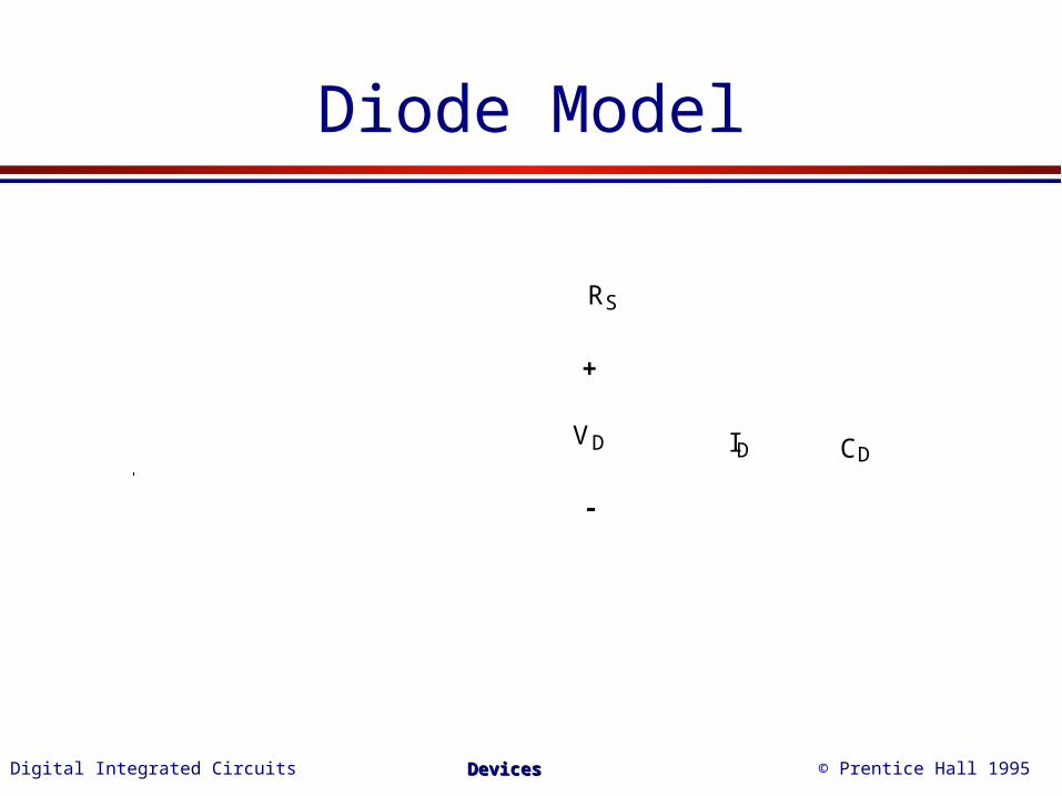
Diode Model
ID
RS
CD
+
-
VD

Digital Integrated Circuits © Prentice Hall 1995DevicesDevices
SPICE Parameters

Digital Integrated Circuits © Prentice Hall 1995DevicesDevices
The MOS Transistor
n+n+
p-substrate
Field-Oxyde
(SiO2)
p+ stopper
Polysilicon
Gate Oxyde
DrainSource
Gate
Bulk Contact
CROSS-SECTION of NMOS Transistor

Digital Integrated Circuits © Prentice Hall 1995DevicesDevices
Cross-Section of CMOS Technology

Digital Integrated Circuits © Prentice Hall 1995DevicesDevices
MOS transistors Types and Symbols
D
S
G
D
S
G
G
S
D D
S
G
NMOS Enhancement NMOS
PMOS
Depletion
Enhancement
B
NMOS withBulk Contact

Digital Integrated Circuits © Prentice Hall 1995DevicesDevices
Threshold Voltage: Concept
n+n+
p-substrate
DSG
B
VGS
+
-
Depletion
Region
n-channel

Digital Integrated Circuits © Prentice Hall 1995DevicesDevices
The Threshold Voltage

Digital Integrated Circuits © Prentice Hall 1995DevicesDevices
Current-Voltage Relations
n+n+
p-substrate
D
SG
B
VGS
xL
V(x) +–
VDS
ID
MOS transistor and its bias conditions

Digital Integrated Circuits © Prentice Hall 1995DevicesDevices
Current-Voltage Relations

Digital Integrated Circuits © Prentice Hall 1995DevicesDevices
Transistor in Saturation
n+n+
S
G
VGS
D
VDS > VGS - VT
VGS - VT+-

Digital Integrated Circuits © Prentice Hall 1995DevicesDevices
I-V Relation
0.0 1.0 2.0 3.0 4.0 5.0
VDS (V)
1
2
I D (
mA
)
0.0 1.0 2.0 3.0VGS (V)
0.010
0.020
÷ I
D
VT
SubthresholdCurrent
Triode Saturation
VGS = 5V
VGS = 3V
VGS = 4V
VGS = 2V
VGS = 1V
(a) ID as a function of VDS (b) ID as a function of VGS
(for VDS = 5V).
Sq
ua
re D
ep
end
en
ce
VDS = VGS-VT
NMOS Enhancement Transistor: W = 100 m, L = 20 m

Digital Integrated Circuits © Prentice Hall 1995DevicesDevices
A model for manual analysis

Digital Integrated Circuits © Prentice Hall 1995DevicesDevices
Dynamic Behavior of MOS Transistor
DS
G
B
CGDCGS
CSB CDBCGB
Digital Integrated Circuits © Prentice Hall 1995DevicesDevices
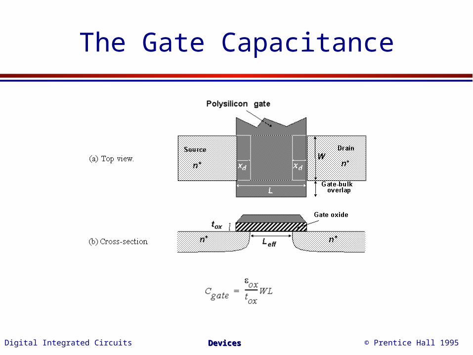
The Gate Capacitance

Digital Integrated Circuits © Prentice Hall 1995DevicesDevices
Average Gate Capacitance
Most important regions in digital design: saturation and cut-off
Different distributions of gate capacitance for varying
operating conditions
Digital Integrated Circuits © Prentice Hall 1995DevicesDevices
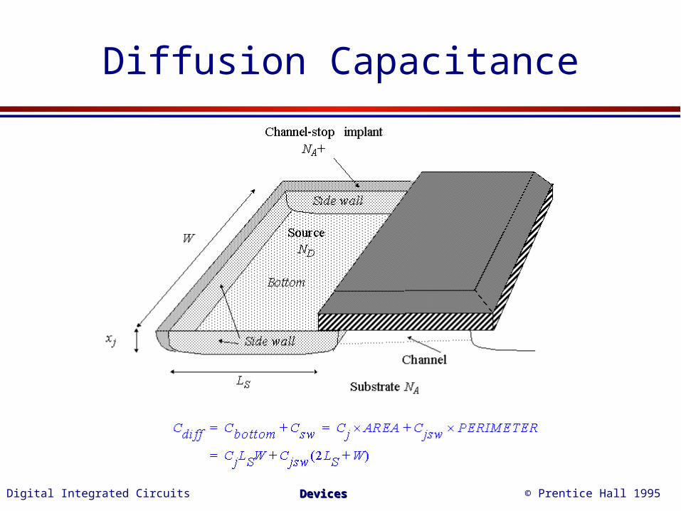
Diffusion Capacitance

Digital Integrated Circuits © Prentice Hall 1995DevicesDevices
Junction Capacitance

Digital Integrated Circuits © Prentice Hall 1995DevicesDevices
Linearizing the Junction Capacitance
Replace non-linear capacitance bylarge-signal equivalent linear capacitance
which displaces equal charge over voltage swing of interest

Digital Integrated Circuits © Prentice Hall 1995DevicesDevices
The Sub-Micron MOS Transistor
• Threshold Variations
• Parasitic Resistances
• Velocity Sauturation and Mobility Degradation
• Subthreshold Conduction
• Latchup

Digital Integrated Circuits © Prentice Hall 1995DevicesDevices
Threshold Variations
VT
L
Long-channel threshold Low VDS threshold
Threshold as a function of the length (for low VDS)
Drain-induced barrier lowering (for low L)

Digital Integrated Circuits © Prentice Hall 1995DevicesDevices
Parasitic Resistances
W
LD
Drain
Draincontact
Polysilicon gate
DS
G
RS RD
VGS,eff

Digital Integrated Circuits © Prentice Hall 1995DevicesDevices
Velocity Saturation (1)
EV/m)Esat
n (c
m/s
ec)
sat = 107
Constant mobility (slope = )
constant velocity
EtV/m)
n (c
m2 /V
s)
n0
(b) Mobility degradation(a) Velocity saturation
0
700
250

Digital Integrated Circuits © Prentice Hall 1995DevicesDevices
Velocity Saturation (2)
VDS (V)
I D (
mA
)
Lin
ea
r D
ep
en
de
nc
e
VGS = 5
VGS = 4
VGS = 3
VGS = 2
VGS = 1
0.0 1.0 2.0 3.0 4.0 5.0
0.5
1.0
1.5
(a) ID as a function of VDS (b) ID as a function of VGS(for VDS = 5 V).
0.0 1.0 2.0 3.0VGS (V)
0
0.5
I D (
mA
)
Linear Dependence on VGS

Digital Integrated Circuits © Prentice Hall 1995DevicesDevices
Sub-Threshold Conduction
0.0 1.0 2.0 3.0VGS (V)
10 12
10 10
10 8
10 6
10 4
10 2
ln(I
D)
(A)
Subthreshold exponential region
Linear region
VT

Digital Integrated Circuits © Prentice Hall 1995DevicesDevices
Latchup
(a) Origin of latchup (b) Equivalent circuit
VDD
Rpsubs
Rnwell p-source
n-source
n+ n+p+ p+ p+ n+
p-substrateRpsubs
Rnwell
VDD
n-well

Digital Integrated Circuits © Prentice Hall 1995DevicesDevices
SPICE MODELS
Level 1: Long Channel Equations - Very Simple
Level 2: Physical Model - Includes VelocitySaturation and Threshold Variations
Level 3: Semi-Emperical - Based on curve fittingto measured devices
Level 4 (BSIM): Emperical - Simple and Popular

Digital Integrated Circuits © Prentice Hall 1995DevicesDevices
MAIN MOS SPICE PARAMETERS

Digital Integrated Circuits © Prentice Hall 1995DevicesDevices
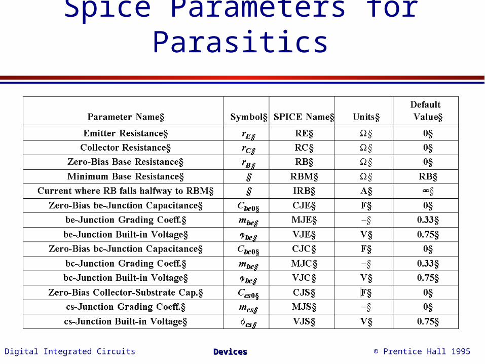
SPICE Parameters for Parasitics

Digital Integrated Circuits © Prentice Hall 1995DevicesDevices
SPICE Transistors Parameters

Digital Integrated Circuits © Prentice Hall 1995DevicesDevices
Fitting level-1 model for manual analysis
VGS = 5 V
VDS = 5 V VDS
ID
Long-channel
approximation
Short-channelI-V curve
Region of
matching
Select k’ and such that best matching is obtained @ Vgs= Vds = VDD

Digital Integrated Circuits © Prentice Hall 1995DevicesDevices
Technology Evolution

Digital Integrated Circuits © Prentice Hall 1995DevicesDevices
Bipolar Transistor
n-epitaxy
p-substrate
n+ buried layer
p+
isolation
n+ p+
pn+
E B C
p+
E C
B
n+ p n
(a) Cross-sectional view.
(b) Idealized transistor structure.

Digital Integrated Circuits © Prentice Hall 1995DevicesDevices
Schematic Symbols and Sign Conventions
C
E
B
IB
IE
IC+
–
+
+
–
–
VBC
VBE
VCE
C
E
B
IB
IE
IC+
–
+
+
–
–
VBC
VBE
VCE
(a) npn (b) pnp

Digital Integrated Circuits © Prentice Hall 1995DevicesDevices
Operations Modes

Digital Integrated Circuits © Prentice Hall 1995DevicesDevices
Forward Active Operation
x
E B C
WB
Carrier Concentration
DepletionRegions
0 W
pe0
pc0
nb0
nb(0)

Digital Integrated Circuits © Prentice Hall 1995DevicesDevices
Current Components
x
E B C
ICIE
IB
1
2 3
electrons
holes

Digital Integrated Circuits © Prentice Hall 1995DevicesDevices
Reverse Active
x
E B C
WB
Carrier Concentration
0 W
pe0nb0
nb(0)
pc0
nb(W)

Digital Integrated Circuits © Prentice Hall 1995DevicesDevices
Saturation Mode
x
E B C
WB
Carrier Concentration
0 W
pe0
nb0
nb(0)
pc0QS
QAnb(W)

Digital Integrated Circuits © Prentice Hall 1995DevicesDevices
Cutoff
x
E B C
WB
Carrier Concentration
0 W
pe0
nb0nb(0)pc0
nb(W)

Digital Integrated Circuits © Prentice Hall 1995DevicesDevices
Bipolar Transistor Operation
0.0 2.0VCE (V)
0
5
10
15
I C(m
A)
-3.0 -1.0
VCE (V)
-0.5
I C (
mA
)
IB=100 A
IB=75 A
IB=50 A
IB=25 A
0
-0.25
IB=25 A
IB=50 A
IB=75 A
IB=100 A
Reverse Operation
Forward Operation
Active
Saturation
Digital Integrated Circuits © Prentice Hall 1995DevicesDevices
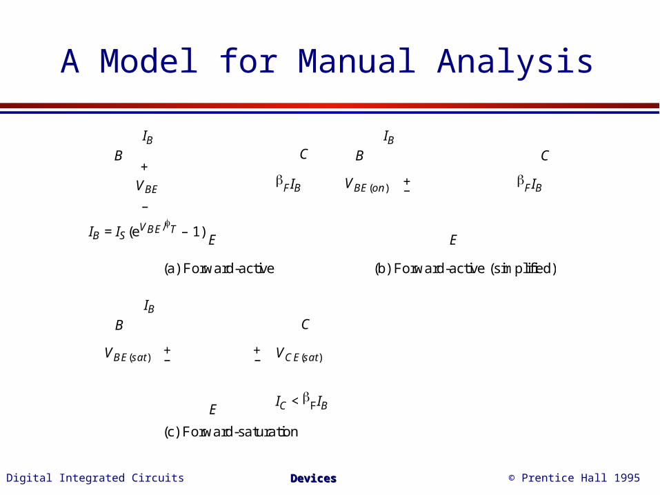
A Model for Manual Analysis
E
CB
FIB
IB
+
–
VBE
IB = IS(eVBE/T – 1)E
CB
FIB
IB
+–VBE(on)
(a) Forward-active (b) Forward-active (simplified)
E
CB
IB
+–VBE(sat)
(c) Forward-saturation
+– VCE(sat)
IC < FIB

Digital Integrated Circuits © Prentice Hall 1995DevicesDevices
Capacitive Model for Bipolar Transistor
C
E
B
QF
QR
Cbe
Cbc
S
Ccs
collector-substratejunction capacitance
base-emitterbase-collector
junction capacitances
base charge

Digital Integrated Circuits © Prentice Hall 1995DevicesDevices
Junction Capacitances

Digital Integrated Circuits © Prentice Hall 1995DevicesDevices
Base Charge - Diffusion Capacitance
Digital Integrated Circuits © Prentice Hall 1995DevicesDevices
Bipolar Transistors - Secondary Effects
• Early Voltage
• Parasitic Resistances
• Beta Variations

Digital Integrated Circuits © Prentice Hall 1995DevicesDevices
Early Voltage
ForwardActive
Saturation
VA
VCE
IC
VBE3
VBE2
VBE1

Digital Integrated Circuits © Prentice Hall 1995DevicesDevices
Parasitic Resistance
n-epitaxy
p-substrate
n+ buried layer
p+
isolation
n+ p+p n+
E B C
p+rC1
rC3
rB
rC2
rE

Digital Integrated Circuits © Prentice Hall 1995DevicesDevices
Beta Variations
VBE (linear)
ln (I)
IC
IB
F
High Level Injection
Recombination
IKF

Digital Integrated Circuits © Prentice Hall 1995DevicesDevices
SPICE models for Bipolar

Digital Integrated Circuits © Prentice Hall 1995DevicesDevices
Main Bipolar Transistor SPICE Models
Digital Integrated Circuits © Prentice Hall 1995DevicesDevices
Spice Parameters for Parasitics

Digital Integrated Circuits © Prentice Hall 1995DevicesDevices
SPICE Transistor Parameters

Digital Integrated Circuits © Prentice Hall 1995DevicesDevices
Process Variations
Devices parameters vary between runs and even on the same die!
Variations in the process parameters, such as impurity concentration den-sities, oxide thicknesses, and diffusion depths. These are caused by non-uniform conditions during the deposition and/or the diffusion of theimpurities. This introduces variations in the sheet resistances and transis-tor parameters such as the threshold voltage.
Variations in the dimensions of the devices, mainly resulting from thelimited resolution of the photolithographic process. This causes (W/L)variations in MOS transistors and mismatches in the emitter areas ofbipolar devices.

Digital Integrated Circuits © Prentice Hall 1995DevicesDevices
Impact of Device Variations
1.10 1.20 1.30 1.40 1.50 1.60
Leff (in mm)
1.50
1.70
1.90
2.10
De
lay
(nse
c)
–0.90 –0.80 –0.70 –0.60 –0.50
VTp (V)
1.50
1.70
1.90
2.10
De
lay
(nse
c)
Delay of Adder circuit as a function of variations in L and VT