Interfacial toughness measurements for thin films on …volinsky/VolinskyActaMatReview2002.pdfdue...
26
Acta Materialia 50 (2002) 441–466 www.elsevier.com/locate/actamat Overview Interfacial toughness measurements for thin films on substrates A.A. Volinsky a , N.R. Moody b , W.W. Gerberich c,* a Motorola Corp., Mesa, AZ 85202, USA b Sandia National Laboratories, Livermore, CA 94551, USA c Department of Chemical Engineering and Materials Science, University of Minnesota, Minneapolis, MN 55455, USA Received 1 May 2001; received in revised form 11 September 2001; accepted 11 September 2001 Abstract There are more than 200 different methods for measuring adhesion, suggesting it to be material, geometry and even industry specific. This availability has exploded at least partly due to the arrival of dissimilar material interfaces and thin films and the ease with which microfabrication techniques apply to silicon technology. Having an eye toward those tests utilized for thin films, this paper reviews only a few of these techniques. The emphasis is on measuring thin film adhesion from the standpoint of fracture mechanics, when the film is mechanically or by other means removed from the substrate, and the amount of energy necessary for this process is calculated per unit area of the removed film. This tends to give values approaching the true work of adhesion at small thickness and greater values of the practical work of adhesion at larger thickness, all being in the 30–30,000 nm range. The resulting large range of toughnesses is shown to be dependent on the scale of plasticity achieved as controlled by film thickness, microstructure, chemistry and test temperature. While the tests reviewed largely address the measurement of elastic strain energy release rates, we also briefly address a few theoretical models which are specific to the resistance side of the delamination equation. The weight of the evidence suggests for ductile metallic films that the major extrinsic variables are film stress, extent of delamination, thickness and temperature while the major intrinsic ones are modulus, yield strength, the thermodynamic work of adhesion and one or more length scales. For some 25 film/substrate multilayers, with emphasis on Al, Au and Cu, the comparison of several theoretical models as to how the extrinsic and intrinsic variables intertwine is made. 2002 Published by Elsevier Science Ltd on behalf of Acta Materialia Inc. Keywords: Fracture & fracture toughness; Thin films; Interface; Adhesion energies 1. Introduction Thin film adhesion is a very important property not only for microelectronics and magnetic rec- * Corresponding author. Tel.: +1-612-625-1313; fax: +1- 612-626-7246. E-mail address: [email protected] (W.W. Gerberich). 1359-6454/02/$22.00 2002 Published by Elsevier Science Ltd on behalf of Acta Materialia Inc. PII:S1359-6454(01)00354-8 ording industries, but also for emerging techno- logies such as data transmission through optical switches which are dependent on microelectro- mechanical systems (MEMS). In general, films that will adhere to the substrate are desired, though spontaneous delamination may occur at any time due to residual stress induced crack growth between the thin film and the substrate. Qualitative
Transcript of Interfacial toughness measurements for thin films on …volinsky/VolinskyActaMatReview2002.pdfdue...
Acta Materialia 50 (2002) 441–466www.elsevier.com/locate/actamat
Overview
Interfacial toughness measurements for thin films onsubstrates
A.A. Volinsky a, N.R. Moodyb, W.W. Gerberichc,*
a Motorola Corp., Mesa, AZ 85202, USAb Sandia National Laboratories, Livermore, CA 94551, USA
c Department of Chemical Engineering and Materials Science, University of Minnesota, Minneapolis, MN 55455, USA
Received 1 May 2001; received in revised form 11 September 2001; accepted 11 September 2001
Abstract
There are more than 200 different methods for measuring adhesion, suggesting it to be material, geometry and evenindustry specific. This availability has exploded at least partly due to the arrival of dissimilar material interfaces and thinfilms and the ease with which microfabrication techniques apply to silicon technology. Having an eye toward those testsutilized for thin films, this paper reviews only a few of these techniques. The emphasis is on measuring thin film adhesionfrom the standpoint of fracture mechanics, when the film is mechanically or by other means removed from the substrate,and the amount of energy necessary for this process is calculated per unit area of the removed film. This tends to givevalues approaching the true work of adhesion at small thickness and greater values of the practical work of adhesion atlarger thickness, all being in the 30–30,000 nm range. The resulting large range of toughnesses is shown to be dependenton the scale of plasticity achieved as controlled by film thickness, microstructure, chemistry and test temperature.
While the tests reviewed largely address the measurement of elastic strain energy release rates, we also briefly addressa few theoretical models which are specific to the resistance side of the delamination equation. The weight of theevidence suggests for ductile metallic films that the major extrinsic variables are film stress, extent of delamination,thickness and temperature while the major intrinsic ones are modulus, yield strength, the thermodynamic work ofadhesion and one or more length scales. For some 25 film/substrate multilayers, with emphasis on Al, Au and Cu, thecomparison of several theoretical models as to how the extrinsic and intrinsic variables intertwine is made. 2002Published by Elsevier Science Ltd on behalf of Acta Materialia Inc.
Keywords: Fracture & fracture toughness; Thin films; Interface; Adhesion energies
1. Introduction
Thin film adhesion is a very important propertynot only for microelectronics and magnetic rec-
* Corresponding author. Tel.:+1-612-625-1313; fax:+1-612-626-7246.
E-mail address: [email protected] (W.W. Gerberich).
1359-6454/02/$22.00 2002 Published by Elsevier Science Ltd on behalf of Acta Materialia Inc.PII: S1359 -6454(01 )00354-8
ording industries, but also for emerging techno-logies such as data transmission through opticalswitches which are dependent on microelectro-mechanical systems (MEMS). In general, films thatwill adhere to the substrate are desired, thoughspontaneous delamination may occur at any timedue to residual stress induced crack growthbetween the thin film and the substrate. Qualitative
442 A.A. Volinsky et al. / Acta Materialia 50 (2002) 441–466
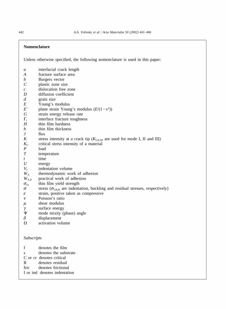
Nomenclature
Unless otherwise specified, the following nomenclature is used in this paper:
a interfacial crack lengthA fracture surface areab Burgers vectorC plastic zone sizec dislocation free zoneD diffusion coefficientd grain sizeE Young’s modulusE� plane strain Young’s modulus (E/(1�v2))G strain energy release rate�i interface fracture toughnessH thin film hardnessh thin film thicknessJ fluxK stress intensity at a crack tip (KI,II,III are used for mode I, II and III)KC critical stress intensity of a materialP loadT temperaturet timeU energyVI indentation volumeWA thermodynamic work of adhesionWA,P practical work of adhesionsys thin film yield strengths stress (sI,B,R are indentation, buckling and residual stresses, respectively)e strain, positive taken as compressiven Poisson’s ratiom shear modulusg surface energy� mode mixity (phase) angled displacement� activation volume
Subscripts
f denotes the films denotes the substrateC or cr denotes criticalR denotes residualfric denotes frictionalI or ind denotes indentation
443A.A. Volinsky et al. / Acta Materialia 50 (2002) 441–466
tests such as the scotch tape test or the pull-off test[1,2], are often used to monitor adhesion, sincethey are quick and easy to perform. While for someapplications the formal comparison is goodenough, quantitative adhesion values are desiredfor understanding factors contributing to thin filmadhesion, for numerical simulations and lifetimepredictions.
Most adhesion tests empirically infer theadhesive strength by subjecting the specimen tosome external load and measuring the critical valueat which it fails [3]. While still useful for routinequality control, these tests do not measure theinterface fracture toughness, since the strain energyrelease rate usually cannot be deconvoluted fromthe work of the external load. Linear Elastic Frac-ture Mechanics (LEFM) is the discipline that pro-vides quantitative answers to specific problems ofcrack propagation from stresses in different struc-tures. It can be also applied in the case of thinfilms.
There are a sufficient number of different tech-niques for measuring thin film adhesion just basedon the LEFM approach. However, there are no uni-versal tests for measuring thin film adhesion. Thiscan be explained by the variety of film systemseven a single industry (e.g. microelectronic) isdealing with. These represent different types ofdissimilar material interfaces that are present inmodern electronic device (metal–metal, metal–cer-amic, polymer–metal, polymer–ceramic, etc.). Asa result, a test that works with one film system maynot necessarily work with another. One should alsonote that adhesion is not a constant, but rather avery complicated variable property, a concept veryimportant for understanding length scale effects insmall volumes.
In this paper different adhesion testing tech-niques will be discussed, along with the fracturetoughness results of mostly metal–ceramic inter-faces. The emphasis will be on as-deposited thinfilms, although some thermally treated and/or dif-fusion-bonded interfaces will be addressed if theseare in the small volume regime arbitrarily definedhere as about 10 µm or less. Though there is nostandard adhesion test for thin films, there are cer-tain universal approaches that can be applied for
measuring film adhesion. However, we must firstdefine adhesion.
2. Definition of adhesion
2.1. True work of adhesion
From a thermodynamic standpoint the true workof adhesion of the interface is the amount of energyrequired to create free surfaces from the bondedmaterials:
WA � gf � gs�gfs (1)
where gf and gs are the specific surface energies ofthe film and the substrate respectively, gfs is theenergy of the interface. True work of adhesion isan intrinsic property of the film/substrate pair; thatdepends on the type of bonding between the filmand the substrate, and the level of initial surfacecontamination.
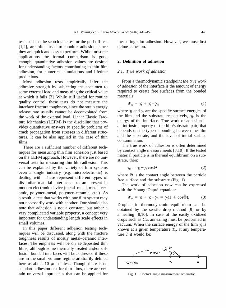
The true work of adhesion is often determinedby contact angle measurements [8,10]. If the testedmaterial particle is in thermal equilibrium on a sub-strate, then:
gfs � gs�gf cos� (2)
where � is the contact angle between the particlefree surface and the substrate (Fig. 1).
The work of adhesion now can be expressedwith the Young–Dupre equation:
WA � gf � gs�gfs � gf(1 � cos�). (3)
Droplets in thermodynamic equilibrium can beobtained by the sessile drop method [9] or byannealing [8,10]. In case of the easily oxidizeddrops such as Cu, annealing must be performed invacuum. When the surface energy of the film gf isknown at a given temperature T0, at any tempera-ture T it would be:
Fig. 1. Contact angle measurement schematic.
444 A.A. Volinsky et al. / Acta Materialia 50 (2002) 441–466
gf(T)�gf(T0) � (T�T0)�∂gf∂T�T � T0
. (4)
Solving Eqs. (3) and (4) for the annealing tempera-ture gives the value of the true (thermodynamic)adhesive energy. In most of the cases annealingmust be performed in vacuum in order to avoidoxidation. If crystallographic faceting occurs uponcooling, a different technique is used to assess thework of adhesion, based on the aspect ratiomeasurements of the equilibrated crystals [6,7].Contact angle distribution can be obtained from theSEM or AFM image analysis [8]. Usually bothresults from contact angle and aspect ratiomeasurements agree well for metallic films [8].
The true work of adhesion is a constant for agiven film/substrate pair, and for metals on ceramicis typically a small number on the order of 0.5–2J/m2. Reimanis et al. [7] and Lipkin et al. [8] meas-ured the thermodynamic work of adhesion of goldon sapphire to be 0.5–0.9 J/m2. Furuya andcoworkers calculated adhesive energies ofCu/SiO2, Cu/TiN and Cu/TiW interfaces using thecontact angle technique [10] with the two lattervalues being more than double the Cu/SiO2 valueof 0.8 J/m2 as discussed later.
For the idealized case of Griffith fracture [4], theinterfacial toughness, �I, is assumed to be equal tothe thermodynamic work of adhesion, WA:�I = WA. In practice, even brittle fracture isaccompanied by some sort of energy dissipationeither through plastic deformation at the crack tip[5], or friction. In this regard, even relatively thinfilms on the order of 100 nm can exhibit plasticityduring interfacial fracture resulting in an elevatedwork of fracture.
2.2. Practical work of adhesion
Most of the test methods measure adhesion bydelaminating thin films from the substrate. Whiledebonding from the substrate, the thin film and/orthe substrate usually experience plastic defor-mation, so it is difficult to extract the true adhesiveenergy from the total energy measured. What ismeasured is the practical work of adhesion, orinterfacial toughness:
WA,P � WA � Uf � Us � Ufric (5)
where Uf and Us are the energy spent in plasticdeformation of the film and the substrate, respect-ively, and Ufric is the energy loss due to friction.Although the last three terms appear to be simplyadditive, it should be noted that both Uf(WA) andUs(WA) are functions of the true work of adhesion[11] and in many cases Ufric(WA) will be as well.Fracture mechanics approach uses the strain energyrelease rate, or the crack driving force as a measureof the practical work of adhesion:
GR, (6)
where U is the total energy of the system, and Ais the crack area, and R is the resistance to crackpropagation. For the films of interest here, theresistance to crack growth is defined as �(�), theinterfacial fracture resistance for mixed modecrack growth. This along with strain energy releaserate, as defined for the case of fixed-grips loading(displacement u0 a constant) condition gives
G � ��∂UE
∂A �u0
�(�) � R. (6a)
We first address the tests to determine G, and laterconsider various resistance terms and several poss-ible ways to interpret that resistance, e.g. phaseangle, friction and plastic energy dissipation.
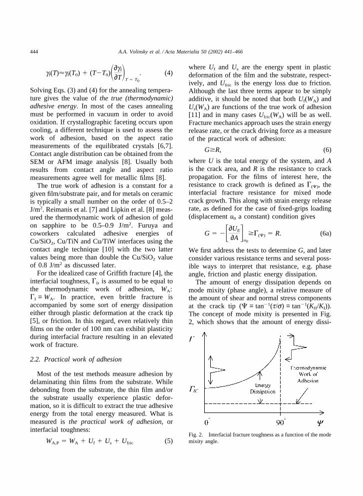
The amount of energy dissipation depends onmode mixity (phase angle), a relative measure ofthe amount of shear and normal stress componentsat the crack tip (� = tan�1(t/s) = tan�1(KII/KI)).The concept of mode mixity is presented in Fig.2, which shows that the amount of energy dissi-
Fig. 2. Interfacial fracture toughness as a function of the modemixity angle.
445A.A. Volinsky et al. / Acta Materialia 50 (2002) 441–466
pation is higher in pure shear compared to the pureopening fracture mode. Severalcriteria/phenomenological relationships have beenproposed to characterize interfacial fracture energyas a function of the phase angle of loading [16].There are results in the literature, both experi-mental and theoretical that exhibit similar behavior[12–16]. The most realistic phenomenologicaldescriptions of the functional dependence of theinterfacial toughness on the mode mixity are givenby Hutchinson and Suo [16]:
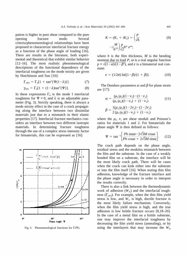
�(�) � �0[1 � tan2{�(1�l)}] (7)
g(�) � �0[1 � (1�l)tan2{�}]. (8)
In these expressions �0 is the mode I interfacialtoughness for � = 0, and l is an adjustable para-meter (Fig. 3). Strictly speaking, there is always amode mixity effect in the case of a crack propagat-ing along the interface between two dissimilarmaterials just due to a mismatch in their elasticproperties [17]. Interfacial fracture mechanics con-siders an interface between two different isotropicmaterials. In determining fracture toughnessthrough the use of a complex stress intensity factorfor bimaterials, this can be expressed as [16]:
Fig. 3. Phenomenological functions for �(�).
K � (K1 � iK2) � � P√h
(9)
�iM
h3/2� p√2
hie eiw,
where h is the film thickness, M is the bendingmoment due to load P, w is a real angular functionp = √(1�a)/(1�b2), and e is a bimaterial real con-stant:
e � (1/2p) ln[(1�b)/(1 � b)]. (10)
The Dundurs parameters a and b for plane strainare [17]:
a �(m1/m2)(1�n2)�(1�n1)
(m1/m2)(1�n2) � (1�n1)(11)
b �12(m1/m2)(1�2n2)�(1�2n1)(m1/m2)(1�n2) � (1�n1)
where the mi, ni are shear moduli and Poisson’sratios for materials 1 and 2. For bimaterials thephase angle � is then defined as follows:
� � tan�1� Ph sinw�2√3M coswPh cosw � 2√3M sinw�. (12)
The crack path depends on the phase angle,residual stress and the modulus mismatch betweenthe film and the substrate. In the case of a weaklybonded film on a substrate, the interface will bethe most likely crack path. There will be caseswhen the crack can kink either into the substrateor into the film itself [16]. When testing thin filmadhesion, knowledge of the fracture interface andthe phase angle is necessary in order to interpretthe results correctly.
There is also a link between the thermodynamicwork of adhesion (WA) and the interfacial tough-ness (�(�)). For example, when the thin film yieldstress is low, and WA is high, ductile fracture isthe most likely failure mechanism. Conversely,when the film yield stress is high, and the trueadhesion is low brittle fracture occurs [8,18–20].In the case of a metal film on a brittle substrate,one may improve the interfacial toughness bydecreasing the film yield stress (annealing), or byusing the interlayers that may increase the WA
446 A.A. Volinsky et al. / Acta Materialia 50 (2002) 441–466
term. We will now consider different techniquesfor measuring the interfacial fracture toughness ofthin films.
3. Adhesion tests classification
There are more than one hundred differentmethods for measuring thin film adhesion thatemploy different sample geometries. Some testsuse continuous films, some require patterning, butall tests use some driving force or stored energyto achieve thin film delamination. The energy maycome from the external mechanical force imposedon the film, or it can be stored in the film itself(through the internal film stress). These tests gener-ally measure critical values of applied stress inten-sity, Ki, or strain energy release rate, Gi where ican be mode I, II or III or of mixed mode character.
3.1. Superlayer test
A test based upon internally developed stresseswas proposed by Bagchi and coworkers [21]. Here,residual tensile stresses in a thin film line drive itsdelamination from a thick substrate. The nondi-mensional steady state strain energy release rate fora narrow line after crack initiation is:
GSSEf/s2f hf � 1/2, (13)
where Ef is the Young’s modulus of the film, hf isthe film thickness, and sf is the residual stress inthe film. The corresponding phase angle in thiscase is about 52° [21]. For the wide line (line widthis greater than its thickness) the residual stress isbiaxial and the strain energy release rate is:
GSSEf/s2f hf � 1�nf, (14)
where nf is Poisson’s ratio of the film. For a typicalfilm thickness of one micron and a residual stress of100 MPa, the stress-induced energy release rate istoo small, on the order of 0.1 J/m2. As most inter-faces in microelectronic devices have higher debondenergies, decohesion is difficult if not impossibleunder these conditions. GSS needs to be increasedwithout substantially changing the phase angle. Oneof the ways to achieve it is by increasing theresulting film thickness by putting a thick overlayer
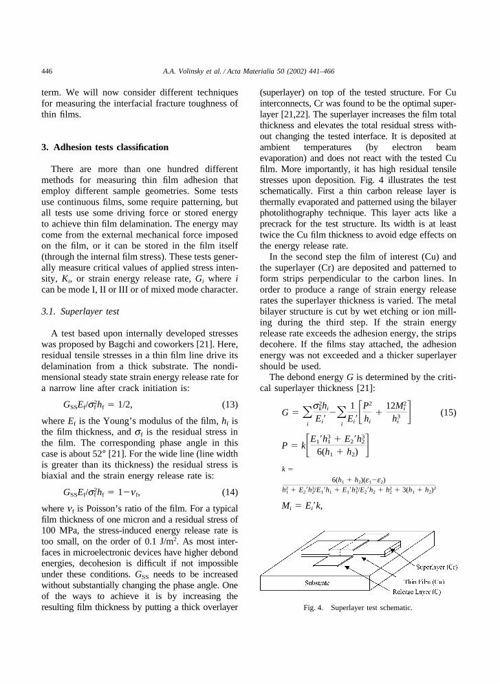
(superlayer) on top of the tested structure. For Cuinterconnects, Cr was found to be the optimal super-layer [21,22]. The superlayer increases the film totalthickness and elevates the total residual stress with-out changing the tested interface. It is deposited atambient temperatures (by electron beamevaporation) and does not react with the tested Cufilm. More importantly, it has high residual tensilestresses upon deposition. Fig. 4 illustrates the testschematically. First a thin carbon release layer isthermally evaporated and patterned using the bilayerphotolithography technique. This layer acts like aprecrack for the test structure. Its width is at leasttwice the Cu film thickness to avoid edge effects onthe energy release rate.
In the second step the film of interest (Cu) andthe superlayer (Cr) are deposited and patterned toform strips perpendicular to the carbon lines. Inorder to produce a range of strain energy releaserates the superlayer thickness is varied. The metalbilayer structure is cut by wet etching or ion mill-ing during the third step. If the strain energyrelease rate exceeds the adhesion energy, the stripsdecohere. If the films stay attached, the adhesionenergy was not exceeded and a thicker superlayershould be used.
The debond energy G is determined by the criti-cal superlayer thickness [21]:
G � �i
s2khi
Ei���
i
1Ei�
�P2
hi
�12M2
i
h3i� (15)
P � k�E1�h31 � E2�h3
2
6(h1 � h2)�
k �
6(h1 � h2)(e1�e2)h2
1 � E2�h32/E1�h1 � E1�h3
1/E2�h2 � h22 � 3(h1 � h2)2
Mi � Ei�k,
Fig. 4. Superlayer test schematic.
447A.A. Volinsky et al. / Acta Materialia 50 (2002) 441–466
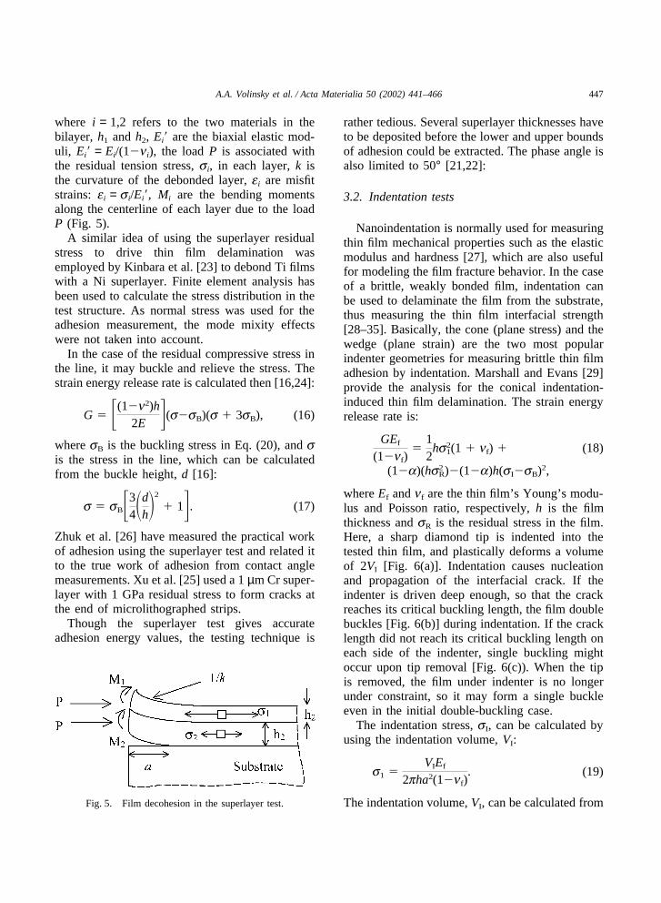
where i = 1,2 refers to the two materials in thebilayer, h1 and h2, Ei� are the biaxial elastic mod-uli, Ei� = Ei/(1�ni), the load P is associated withthe residual tension stress, si, in each layer, k isthe curvature of the debonded layer, ei are misfitstrains: ei = si/Ei�, Mi are the bending momentsalong the centerline of each layer due to the loadP (Fig. 5).
A similar idea of using the superlayer residualstress to drive thin film delamination wasemployed by Kinbara et al. [23] to debond Ti filmswith a Ni superlayer. Finite element analysis hasbeen used to calculate the stress distribution in thetest structure. As normal stress was used for theadhesion measurement, the mode mixity effectswere not taken into account.
In the case of the residual compressive stress inthe line, it may buckle and relieve the stress. Thestrain energy release rate is calculated then [16,24]:
G � �(1�n2)h2E �(s�sB)(s � 3sB), (16)
where sB is the buckling stress in Eq. (20), and sis the stress in the line, which can be calculatedfrom the buckle height, d [16]:
s � sB�34�d
h�2
� 1�. (17)
Zhuk et al. [26] have measured the practical workof adhesion using the superlayer test and related itto the true work of adhesion from contact anglemeasurements. Xu et al. [25] used a 1 µm Cr super-layer with 1 GPa residual stress to form cracks atthe end of microlithographed strips.
Though the superlayer test gives accurateadhesion energy values, the testing technique is
Fig. 5. Film decohesion in the superlayer test.
rather tedious. Several superlayer thicknesses haveto be deposited before the lower and upper boundsof adhesion could be extracted. The phase angle isalso limited to 50° [21,22]:
3.2. Indentation tests
Nanoindentation is normally used for measuringthin film mechanical properties such as the elasticmodulus and hardness [27], which are also usefulfor modeling the film fracture behavior. In the caseof a brittle, weakly bonded film, indentation canbe used to delaminate the film from the substrate,thus measuring the thin film interfacial strength[28–35]. Basically, the cone (plane stress) and thewedge (plane strain) are the two most popularindenter geometries for measuring brittle thin filmadhesion by indentation. Marshall and Evans [29]provide the analysis for the conical indentation-induced thin film delamination. The strain energyrelease rate is:
GEf
(1�nf)�
12
hs21(1 � nf) � (18)
(1�a)(hs2R)�(1�a)h(sI�sB)2,
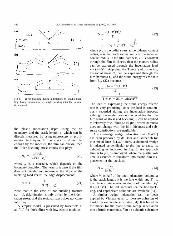
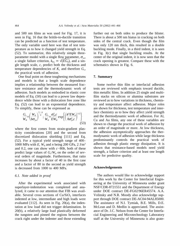
where Ef and nf are the thin film’s Young’s modu-lus and Poisson ratio, respectively, h is the filmthickness and sR is the residual stress in the film.Here, a sharp diamond tip is indented into thetested thin film, and plastically deforms a volumeof 2VI [Fig. 6(a)]. Indentation causes nucleationand propagation of the interfacial crack. If theindenter is driven deep enough, so that the crackreaches its critical buckling length, the film doublebuckles [Fig. 6(b)] during indentation. If the cracklength did not reach its critical buckling length oneach side of the indenter, single buckling mightoccur upon tip removal [Fig. 6(c)). When the tipis removed, the film under indenter is no longerunder constraint, so it may form a single buckleeven in the initial double-buckling case.
The indentation stress, sI, can be calculated byusing the indentation volume, VI:
s1 �VIEf
2pha2(1�nf). (19)
The indentation volume, VI, can be calculated from
448 A.A. Volinsky et al. / Acta Materialia 50 (2002) 441–466
Fig. 6. (a) No buckling during indentation; (b) double-buck-ling during indentation; (c) single-buckling after the indentertip removal.
the plastic indentation depth using the tipgeometry, and the crack length, a, which can bedirectly measured by using microscopy or profil-ometry techniques. If the crack is driven farenough by the indenter, the film can buckle, thenthe Euler buckling stress comes into play:
sB �m2h2Ef
12a2(1�nf), (20)
where m is a constant, which depends on theboundary condition. The term a is zero if the filmdoes not buckle, and represents the slope of thebuckling load versus the edge displacement:
a � 1�1
1 � 0.902(1�nf). (21)
Note that in the case of non-buckling fracture(a = 1), delamination is only driven by the inden-tation stress, and the residual stress does not comeinto play.
A simpler model is presented by Rosenfeld etal. [30] for thick films with low elastic modulus:
G �2(1�n2
f )s2rxh
Ef(22)
� 11 � nf � (a/x)2(1�nf)
�2
,
where srx is the radial stress at the indenter contactradius, a is the crack radius and x is the indentercontact radius. If the film hardness, H, is constantthrough the film thickness, then the contact radiuscan be expressed through the indentation loadx = (P/H)1/2. Applying the Tresca yield criterion,the radial stress srx can be expressed through thefilm hardness H, and the strain energy release ratefrom Eq. (22) becomes:
G �0.627H2h(1�n2
f )Ef
(23)
1[1 � nf � 2(1�nf)Ha2/P]2.
The idea of expressing the strain energy releaserate is very promising, since the load is continu-ously recorded during the indentation process,although the model does not account for the thinfilm residual stress and buckling. It can be appliedto relatively thick films (10 µm), where hardnessdoes not change with the film thickness and sub-strate contributions are negligible.
A microwedge wedge indentation test (MWIT)has been proposed by de Boer and Gerberich forthin metal lines [31,32]. Here, a diamond wedgeis indented perpendicular to the line to cause itsdebonding as indicated in Fig. 6. An approachsimilar to [29] is employed, where the plastic vol-ume is assumed to transform into elastic film dis-placement at the crack tip:
G �Ef�V2
0
2b2ha2, (24)
where V0 is half of the total indentation volume, ais the crack length, b is the line width, and Ef� isthe plane strain elastic modulus of the film: Ef�= Ef/(1�n2
f ). The test accounts for the line buck-ling, and appropriate solutions are available [31].
A similar wedge indentation test has beenapplied by Vlassak et al. to measure adhesion ofhard films on ductile substrates [34]. It is based onthe model for the plane strain wedge indentationinto a brittle continuous film on a ductile substrate:
449A.A. Volinsky et al. / Acta Materialia 50 (2002) 441–466
G �(1�n2
f )sxxh2Ef
, (25)
where sxx is the stress in the film, perpendicular tothe wedge line:
sxx � sR�nf� Ef
1�n2f�W2 tanbpa2 . (26)
Here, sR is the residual stress in the film, W isthe half width of the wedge indentation, b is theinclination of the face of the wedge to the surfaceof the film, and a is the crack length.
The advantage of the wedge indenter geometryover conical, Vickers and Berkovich geometries isthe weaker 1/a2 dependence in Eqs. (24) and (26)compared to 1/a4 for the axisymmetric case [Eqs.(18) and (23)]. The problem with the wedge inden-tation is the alignment. Usually, wedges are notperfectly symmetric and difficult to align perpen-dicular to the plane of the thin film. Misalignmentcauses asymmetric crack growth on both sides ofthe wedge. This effect has been observed on boththe micro and macro scales [31,36]. A new revisionof the wedge indentation test is provided in [37].
A relatively new idea of a cross-sectional inden-tation test for thin film delamination has been pro-posed by Sanchez et al. [38]. An indentation ismade into the substrate cross-section close to thefilm interface which causes the film to debond. Theenergy release rate can be calculated by knowingthe maximum film deflection u0:
G �Eh3u2
0
12(a�b)2(1�l)4(2F � lF�). (27)
where a and b are the delamination and contactradii, respectively, l = a/b, and F is defined as:
F(l) �
2 lnl �1 � l1�l
ln2l
[(1 � l) lnl � 2(1�l)]2, (28)
and F� = dF/dl. This test is particularly useful, asthe film is not directly indented, and the crackinitiates in the brittle substrate, which limits theamount of plastic deformation.
Unfortunately, indentation tests cannot often beused to test adhesion of ductile films on brittle sub-strates. A ductile strongly adhered film most often
deforms before delamination from the substrate.Even if the film debonds from the substrate,delaminations are not reproducible. However, theseproblems have been solved with the introductionof the superlayer indentation technique.
3.3. Superlayer indentation test
Kriese and Gerberich [39] have combined theidea of the superlayer test with the indentation frac-ture test. Deposition of a highly stressed hardsuperlayer on top of the film of interest addsadditional stress to the delamination process, andprevents out of plane displacements of the film,suppressing plastic pile-up around the indenter. Amodified Marshall and Evans analysis has beenused [29], and the laminate theory is employed inorder to calculate necessary terms in Eq. (18) forthe bilayer [39].
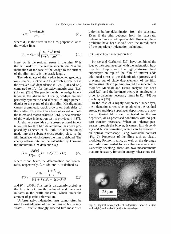
In the case of a highly compressed superlayer,the indentation stress is being added to the residualstress, so multiple superlayer depositions are avo-ided. Blanket films can be tested in the as-deposited, or as-processed conditions with no pat-tern transfer necessary. When an indenter pen-etrates through the bilayer, it causes film debond-ing and blister formation, which can be viewed inan optical microscope using Nomarski contrast(Fig. 7). Properties of the films such as elasticmodulus, Poisson’s ratio, as well as the tip angleand radius are needed for an adhesion assessment.Generally speaking, there are two measurementsthat are necessary for strain energy release rate cal-
Fig. 7. Optical micrographs of indentation induced blisterswith (right) and without (left) a W superlayer.
450 A.A. Volinsky et al. / Acta Materialia 50 (2002) 441–466
culations. From the standpoint of blister formation,both indentation depth and blister diameter arerequired. Blister diameter is measured in theoptical microscope with Nomarski contrast. Usingthe Oliver–Pharr method [27], inelastic indentationdepth, dpl, is calculated from:
P � A(d�dpl)m, (29)
where P and d are the load and displacement from65% of the unloading slope of the load–displace-ment curve, respectively. A and m are the powerlaw fitting parameters. Indentation volume, VI iscalculated from the inelastic depth by using tipgeometry. Now the indentation stress can be calcu-lated from Eq. (19), assuming the conservationof volume.
The solution for the buckling stress in the bilayeris also provided in [39]. There are two differentcases of buckling in the indentation-induceddelamination. If the crack is driven far enough, thefilm may buckle around the indenter when the tipis in contact with the film (double or annularbuckling). The film may also buckle back upon thetip retrieval from the film (single buckling), whenthe total crack length exceeds the critical bucklinglength. See Fig. 6. The appropriate strain energyrelease rate, G can be determined according to thefollowing rule:
(i) G = Gnonbuckled if the total stresses in the filmnever exceed double or single buckling stress-es;
(ii) G = Gnonbuckled if G exceeds Gsingle, but thestress is not sufficient for the double bucklingto happen;
(iii) G = Gdouble if double buckling occurs and Gexceeds Gsingle;
(iv) G = Gsingle if none of the above conditionsoccurs.
Although the residual stress does not come intoplay if the single film is not buckled [Eq. (18)],the situation may change in the case of a bilayerdue to the residual stress in each of the films. Theresidual stress is typically tensile for a metallic film(Cu, Al, Au, etc.) on a Si wafer mostly due to thethermal mismatch (a metal has a higher thermalexpansion coefficient than ceramics). The stress in
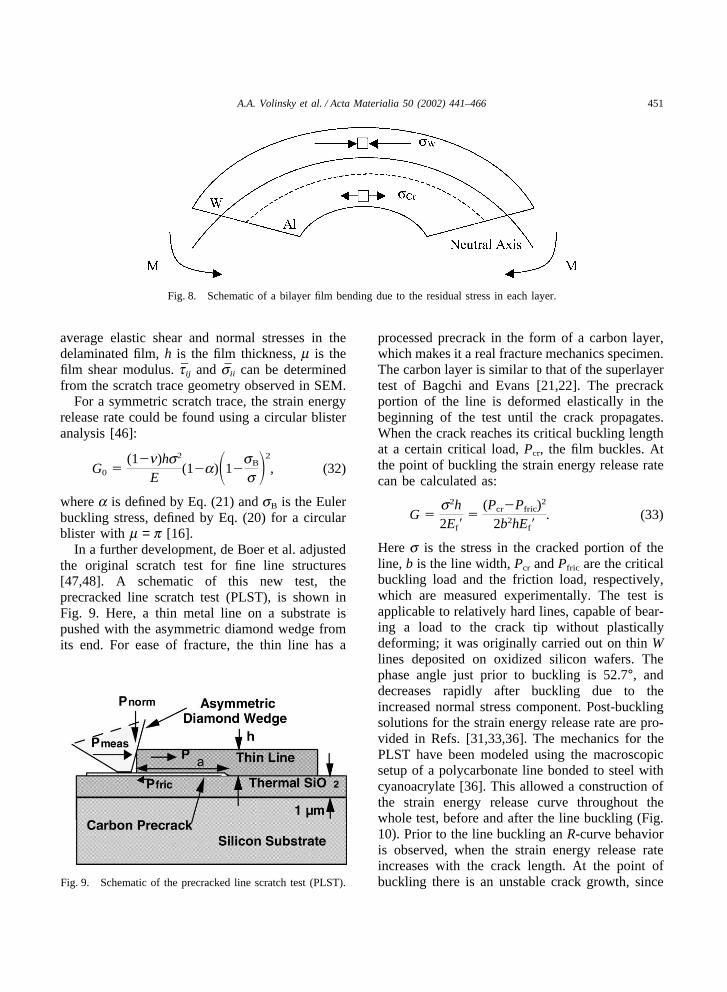
the superlayer is preferred to be compressive [40].In the case of a compressive residual stress in thesuperlayer (W) and tensile stress in the underlayer(Cu), both stresses would contribute to the positivebimaterial beam bending moment, thus the totalcurvature change (Fig. 8). A similar situation hasbeen observed in the case of the bimaterial linesdebonding [24]. The fact that the films are bent inthe freestanding form means that the critical buck-ling stress needs to be reduced accordingly toaccount for the film curvature [41].
The advantage of the superlayer indentation testis that it provides interfacial toughness measure-ments over a wide range of phase angles. Prior tobuckling the phase angle is equal to the real angu-lar function, w, and at the onset of buckling a rapiddecrease occurs.
3.4. Scratch tests
In a typical scratch test a stylus or a diamondtip is drawn across the film surface. The test couldbe treated as a combination of two operations: nor-mal indentation process and horizontal tip motion.A vertical increasing load is applied to the tip dur-ing scratching until the coating detaches from thesubstrate. The minimum critical load Pcr at whichdelamination occurs is used as a measure of thepractical work of adhesion [42,43]:
Pcr �pr2
2 �2EWA,P
h �1/2
, (30)
where r is the contact radius and h is the film thick-ness. This analysis is applicable only when the ten-sile stress normal to the film surface drives delami-nation.
Venkataraman et al. developed a model for esti-mating the energy per unit area G0 stored in thefilm from the scratch elastic stress distribution[44,45], which was modified later to account forresidual stresses in the film [83]:
G0 �(1�n2)s2
r h2E
� ��(1�n2)t2ijh2m
(31)
�(1�n2)s2
iih2E �,
where sr is the residual stress, tij and sii are the
451A.A. Volinsky et al. / Acta Materialia 50 (2002) 441–466
Fig. 8. Schematic of a bilayer film bending due to the residual stress in each layer.
average elastic shear and normal stresses in thedelaminated film, h is the film thickness, m is thefilm shear modulus. tij and sii can be determinedfrom the scratch trace geometry observed in SEM.
For a symmetric scratch trace, the strain energyrelease rate could be found using a circular blisteranalysis [46]:
G0 �(1�n)hs2
E(1�a)�1�
sB
s �2
, (32)
where a is defined by Eq. (21) and sB is the Eulerbuckling stress, defined by Eq. (20) for a circularblister with m = p [16].
In a further development, de Boer et al. adjustedthe original scratch test for fine line structures[47,48]. A schematic of this new test, theprecracked line scratch test (PLST), is shown inFig. 9. Here, a thin metal line on a substrate ispushed with the asymmetric diamond wedge fromits end. For ease of fracture, the thin line has a
Fig. 9. Schematic of the precracked line scratch test (PLST).
processed precrack in the form of a carbon layer,which makes it a real fracture mechanics specimen.The carbon layer is similar to that of the superlayertest of Bagchi and Evans [21,22]. The precrackportion of the line is deformed elastically in thebeginning of the test until the crack propagates.When the crack reaches its critical buckling lengthat a certain critical load, Pcr, the film buckles. Atthe point of buckling the strain energy release ratecan be calculated as:
G �s2h2Ef�
�(Pcr�Pfric)2
2b2hEf�. (33)
Here s is the stress in the cracked portion of theline, b is the line width, Pcr and Pfric are the criticalbuckling load and the friction load, respectively,which are measured experimentally. The test isapplicable to relatively hard lines, capable of bear-ing a load to the crack tip without plasticallydeforming; it was originally carried out on thin Wlines deposited on oxidized silicon wafers. Thephase angle just prior to buckling is 52.7°, anddecreases rapidly after buckling due to theincreased normal stress component. Post-bucklingsolutions for the strain energy release rate are pro-vided in Refs. [31,33,36]. The mechanics for thePLST have been modeled using the macroscopicsetup of a polycarbonate line bonded to steel withcyanoacrylate [36]. This allowed a construction ofthe strain energy release curve throughout thewhole test, before and after the line buckling (Fig.10). Prior to the line buckling an R-curve behavioris observed, when the strain energy release rateincreases with the crack length. At the point ofbuckling there is an unstable crack growth, since
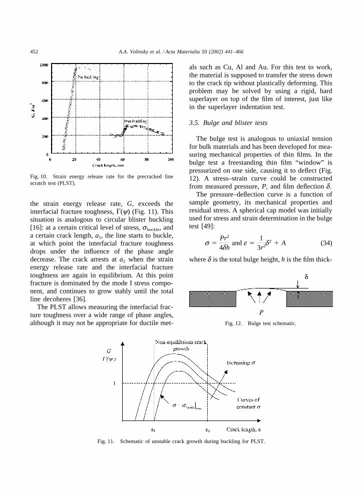
452 A.A. Volinsky et al. / Acta Materialia 50 (2002) 441–466
Fig. 10. Strain energy release rate for the precracked linescratch test (PLST).
the strain energy release rate, G, exceeds theinterfacial fracture toughness, �(y) (Fig. 11). Thissituation is analogous to circular blister buckling[16]: at a certain critical level of stress, sbuckle, anda certain crack length, a1, the line starts to buckle,at which point the interfacial fracture toughnessdrops under the influence of the phase angledecrease. The crack arrests at a2 when the strainenergy release rate and the interfacial fracturetoughness are again in equilibrium. At this pointfracture is dominated by the mode I stress compo-nent, and continues to grow stably until the totalline decoheres [36].
The PLST allows measuring the interfacial frac-ture toughness over a wide range of phase angles,although it may not be appropriate for ductile met-
Fig. 11. Schematic of unstable crack growth during buckling for PLST.
als such as Cu, Al and Au. For this test to work,the material is supposed to transfer the stress downto the crack tip without plastically deforming. Thisproblem may be solved by using a rigid, hardsuperlayer on top of the film of interest, just likein the superlayer indentation test.
3.5. Bulge and blister tests
The bulge test is analogous to uniaxial tensionfor bulk materials and has been developed for mea-suring mechanical properties of thin films. In thebulge test a freestanding thin film “window” ispressurized on one side, causing it to deflect (Fig.12). A stress–strain curve could be constructedfrom measured pressure, P, and film deflection d.
The pressure–deflection curve is a function ofsample geometry, its mechanical properties andresidual stress. A spherical cap model was initiallyused for stress and strain determination in the bulgetest [49]:
s �Pr2
4dhand e �
13r2d
2 � A (34)
where d is the total bulge height, h is the film thick-
Fig. 12. Bulge test schematic.
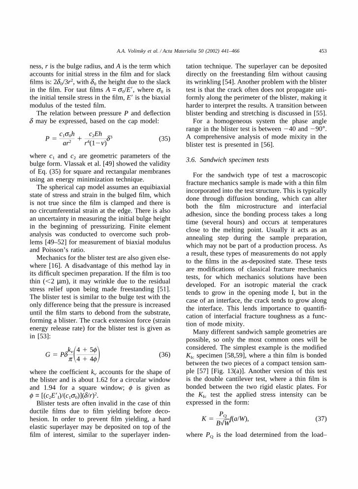
453A.A. Volinsky et al. / Acta Materialia 50 (2002) 441–466
ness, r is the bulge radius, and A is the term whichaccounts for initial stress in the film and for slackfilms is: 2d0/3r2, with d0 the height due to the slackin the film. For taut films A = s0/E�, where s0 isthe initial tensile stress in the film, E� is the biaxialmodulus of the tested film.
The relation between pressure P and deflectiond may be expressed, based on the cap model:
P �c1s0h
ar2 �c2Eh
r4(1�n)d3 (35)
where c1 and c2 are geometric parameters of thebulge form. Vlassak et al. [49] showed the validityof Eq. (35) for square and rectangular membranesusing an energy minimization technique.
The spherical cap model assumes an equibiaxialstate of stress and strain in the bulged film, whichis not true since the film is clamped and there isno circumferential strain at the edge. There is alsoan uncertainty in measuring the initial bulge heightin the beginning of pressurizing. Finite elementanalysis was conducted to overcome such prob-lems [49–52] for measurement of biaxial modulusand Poisson’s ratio.
Mechanics for the blister test are also given else-where [16]. A disadvantage of this method lay inits difficult specimen preparation. If the film is toothin (�2 µm), it may wrinkle due to the residualstress relief upon being made freestanding [51].The blister test is similar to the bulge test with theonly difference being that the pressure is increaseduntil the film starts to debond from the substrate,forming a blister. The crack extension force (strainenergy release rate) for the blister test is given asin [53]:
G � Pdknp�4 � 5f
4 � 4f� (36)
where the coefficient kn accounts for the shape ofthe blister and is about 1.62 for a circular windowand 1.94 for a square window; f is given asf = [(c2E�f)/(c1s0)](d/r)2.
Blister tests are often invalid in the case of thinductile films due to film yielding before deco-hesion. In order to prevent film yielding, a hardelastic superlayer may be deposited on top of thefilm of interest, similar to the superlayer inden-
tation technique. The superlayer can be depositeddirectly on the freestanding film without causingits wrinkling [54]. Another problem with the blistertest is that the crack often does not propagate uni-formly along the perimeter of the blister, making itharder to interpret the results. A transition betweenblister bending and stretching is discussed in [55].
For a homogeneous system the phase anglerange in the blister test is between �40 and �90°.A comprehensive analysis of mode mixity in theblister test is presented in [56].
3.6. Sandwich specimen tests
For the sandwich type of test a macroscopicfracture mechanics sample is made with a thin filmincorporated into the test structure. This is typicallydone through diffusion bonding, which can alterboth the film microstructure and interfacialadhesion, since the bonding process takes a longtime (several hours) and occurs at temperaturesclose to the melting point. Usually it acts as anannealing step during the sample preparation,which may not be part of a production process. Asa result, these types of measurements do not applyto the films in the as-deposited state. These testsare modifications of classical fracture mechanicstests, for which mechanics solutions have beendeveloped. For an isotropic material the cracktends to grow in the opening mode I, but in thecase of an interface, the crack tends to grow alongthe interface. This lends importance to quantifi-cation of interfacial fracture toughness as a func-tion of mode mixity.
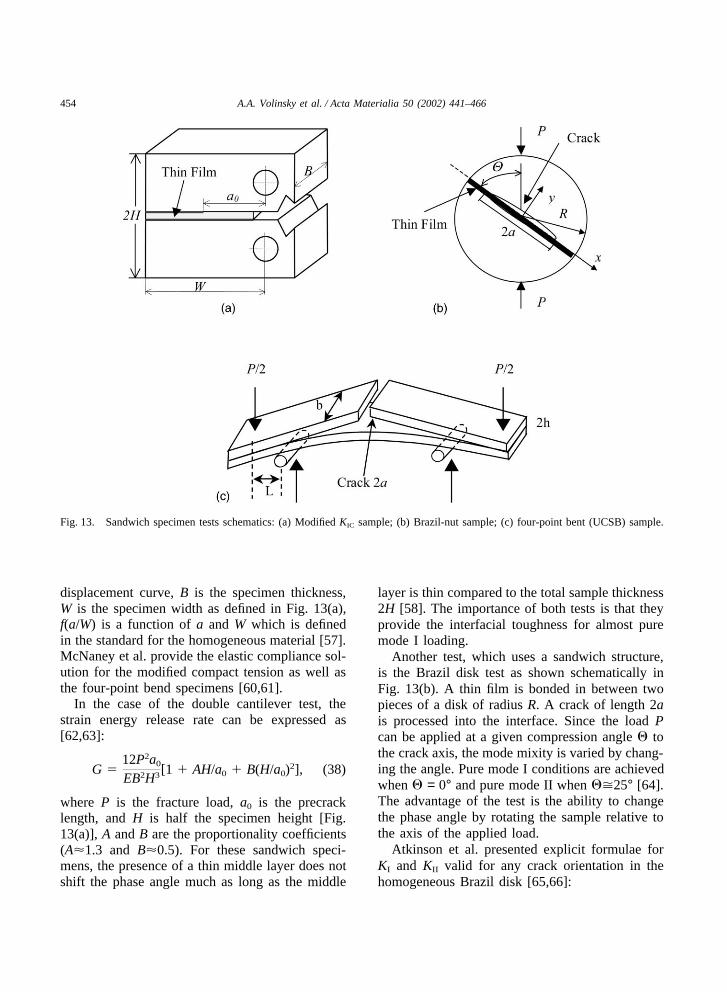
Many different sandwich sample geometries arepossible, so only the most common ones will beconsidered. The simplest example is the modifiedKIc specimen [58,59], where a thin film is bondedbetween the two pieces of a compact tension sam-ple [57] [Fig. 13(a)]. Another version of this testis the double cantilever test, where a thin film isbonded between the two rigid elastic plates. Forthe KIc test the applied stress intensity can beexpressed in the form:
K �PQ
B√Wf(a/W), (37)
where PQ is the load determined from the load–
454 A.A. Volinsky et al. / Acta Materialia 50 (2002) 441–466
Fig. 13. Sandwich specimen tests schematics: (a) Modified KIC sample; (b) Brazil-nut sample; (c) four-point bent (UCSB) sample.
displacement curve, B is the specimen thickness,W is the specimen width as defined in Fig. 13(a),f(a/W) is a function of a and W which is definedin the standard for the homogeneous material [57].McNaney et al. provide the elastic compliance sol-ution for the modified compact tension as well asthe four-point bend specimens [60,61].
In the case of the double cantilever test, thestrain energy release rate can be expressed as[62,63]:
G �12P2a0
EB2H3[1 � AH/a0 � B(H/a0)2], (38)
where P is the fracture load, a0 is the precracklength, and H is half the specimen height [Fig.13(a)], A and B are the proportionality coefficients(A�1.3 and B�0.5). For these sandwich speci-mens, the presence of a thin middle layer does notshift the phase angle much as long as the middle
layer is thin compared to the total sample thickness2H [58]. The importance of both tests is that theyprovide the interfacial toughness for almost puremode I loading.
Another test, which uses a sandwich structure,is the Brazil disk test as shown schematically inFig. 13(b). A thin film is bonded in between twopieces of a disk of radius R. A crack of length 2ais processed into the interface. Since the load Pcan be applied at a given compression angle � tothe crack axis, the mode mixity is varied by chang-ing the angle. Pure mode I conditions are achievedwhen � = 0° and pure mode II when ��25° [64].The advantage of the test is the ability to changethe phase angle by rotating the sample relative tothe axis of the applied load.
Atkinson et al. presented explicit formulae forKI and KII valid for any crack orientation in thehomogeneous Brazil disk [65,66]:
455A.A. Volinsky et al. / Acta Materialia 50 (2002) 441–466
KI �PNI
RB�ap
(39)
KII �PNII
RB �ap
where P is the load applied in compression, a ishalf the crack length, B is the disk thickness, NI
and NII are non-dimensional functions of the rela-tive crack size, (a/R), and the compression angle�. O’Dowd and coworkers provided stress inten-sity solution for a bimaterial Brazil disk [64]:
K �YP2R
√2a(2a)�ie ei� (40)
where Y is a dimensionless geometric factor, e isthe bimaterial real constant as in Eq. (10). Thedependence of � and Y on the compression angle� is not known. Since the crack has two tips, thestress intensity factors at each tip will also be dif-ferent, so � and Y must be provided for each cracktip. Brazil disk mechanics for orthotropic materialsas well as an FEM model are discussed in Ref.[67]. Mechanics for a Brazil-nut-sandwich speci-men [Fig. 13(b)] and different failure types areconsidered in [68].
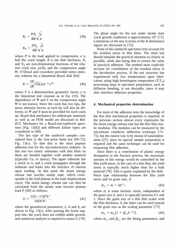
The last type of the sandwich samples con-sidered here is the four-point bend test [69–72],Fig. 13(c). To date this is the most popularadhesion test for the microelectronics industry. Inthis test two elastic substrates with thin films onthem are bonded together with another material(typically Cu, or epoxy). The upper substrate hasa notch in it, and a crack propagates through thesubstrate and kinks into the interface of interestupon loading. At this point the strain energyrelease rate reaches steady state, which corre-sponds to the load plateau in the load–displacementcurve. The strain energy release rate can then becalculated from the steady state fracture plateauload P [69] as follows:
G �21(1�n2)P2L2
16Eb2h3 , (41)
where the geometrical parameters, L, b and h, areshown in Fig. 13(c). After passing the lower sup-port line, the crack does not exhibit stable growth,and numerical analysis is required to assess G [70].
The phase angle for the test under steady statecrack growth conditions is approximately 43° [71].Limitations of the test in terms of the K-dominanceregion are discussed in [72].
None of the sandwich specimen tests account forthe residual stress in thin films. The ideal testshould simulate the practical situation as closely aspossible, while also being able to extract the valueof practical adhesion. The method must explicitlyaccount for contribution of the residual stress tothe decohesion process. If the test structure hasexperienced only low temperatures upon fabri-cation, using high homologous temperature (T/Tm)processing steps in specimen preparation, such asdiffusion bonding, is not desirable, since it mayalter interface adhesion properties.
4. Mechanical properties determination
For most of the adhesion tests the knowledge ofthe thin film mechanical properties is required. Inthe previous section almost every expression forthe strain energy release rate has the thin film elas-tic modulus. The modulus can be measured by themicrobeam cantilever deflection technique [73–75], but the easiest way is by means of nanoindent-ation [27], since no special sample preparation isrequired and the same technique can be used formeasuring film adhesion.
Since there is a contribution of plastic energydissipation to the fracture process, the maximumamount of this energy would be controlled by thefilm yield stress. In the case of a thin film, the yieldstress is typically much higher than for a bulkmaterial [76]. This is partly explained by the Hall–Petch type relationship between the film yieldstress and its grain size, d:
sys � si � kd�n, (42)
where si is some intrinsic stress, independent ofthe grain size d, and n is typically between 0.5 and1. Since the grain size of a thin film scales withthe film thickness, h, the latter can be used insteadof the grain size as the scaling parameter [77]:
sys � sCu[1 � bCuh�1/2], (43)
where sCu and bCu are the fitting parameters, and
456 A.A. Volinsky et al. / Acta Materialia 50 (2002) 441–466
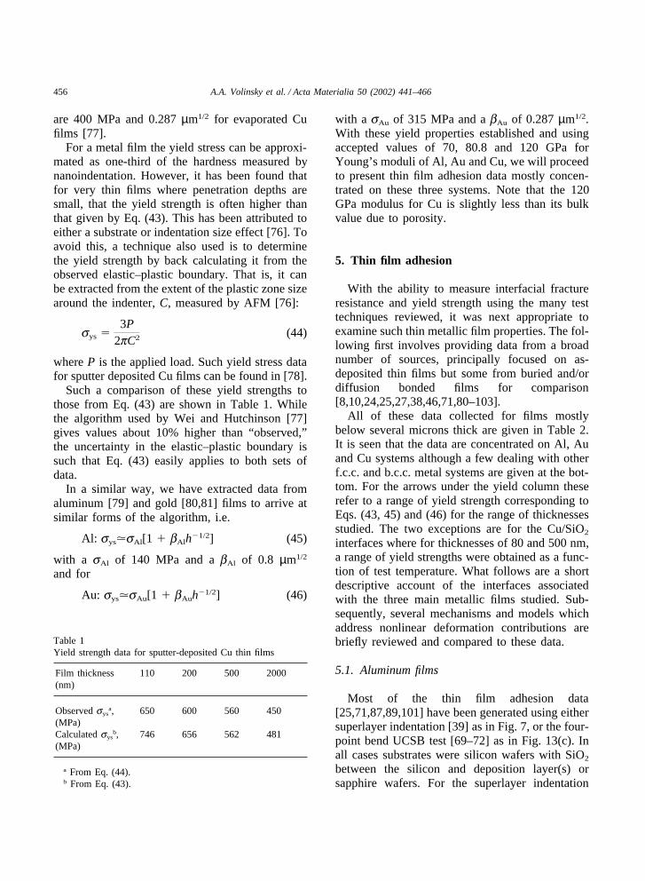
are 400 MPa and 0.287 µm1/2 for evaporated Cufilms [77].
For a metal film the yield stress can be approxi-mated as one-third of the hardness measured bynanoindentation. However, it has been found thatfor very thin films where penetration depths aresmall, that the yield strength is often higher thanthat given by Eq. (43). This has been attributed toeither a substrate or indentation size effect [76]. Toavoid this, a technique also used is to determinethe yield strength by back calculating it from theobserved elastic–plastic boundary. That is, it canbe extracted from the extent of the plastic zone sizearound the indenter, C, measured by AFM [76]:
sys �3P
2pC2 (44)
where P is the applied load. Such yield stress datafor sputter deposited Cu films can be found in [78].
Such a comparison of these yield strengths tothose from Eq. (43) are shown in Table 1. Whilethe algorithm used by Wei and Hutchinson [77]gives values about 10% higher than “observed,”the uncertainty in the elastic–plastic boundary issuch that Eq. (43) easily applies to both sets ofdata.
In a similar way, we have extracted data fromaluminum [79] and gold [80,81] films to arrive atsimilar forms of the algorithm, i.e.
Al: syssAl[1 � bAlh�1/2] (45)
with a sAl of 140 MPa and a bAl of 0.8 µm1/2
and for
Au: syssAu[1 � bAuh�1/2] (46)
Table 1Yield strength data for sputter-deposited Cu thin films
Film thickness 110 200 500 2000(nm)
Observed sysa, 650 600 560 450
(MPa)Calculated sys
b, 746 656 562 481(MPa)
a From Eq. (44).b From Eq. (43).
with a sAu of 315 MPa and a bAu of 0.287 µm1/2.With these yield properties established and usingaccepted values of 70, 80.8 and 120 GPa forYoung’s moduli of Al, Au and Cu, we will proceedto present thin film adhesion data mostly concen-trated on these three systems. Note that the 120GPa modulus for Cu is slightly less than its bulkvalue due to porosity.
5. Thin film adhesion
With the ability to measure interfacial fractureresistance and yield strength using the many testtechniques reviewed, it was next appropriate toexamine such thin metallic film properties. The fol-lowing first involves providing data from a broadnumber of sources, principally focused on as-deposited thin films but some from buried and/ordiffusion bonded films for comparison[8,10,24,25,27,38,46,71,80–103].
All of these data collected for films mostlybelow several microns thick are given in Table 2.It is seen that the data are concentrated on Al, Auand Cu systems although a few dealing with otherf.c.c. and b.c.c. metal systems are given at the bot-tom. For the arrows under the yield column theserefer to a range of yield strength corresponding toEqs. (43, 45) and (46) for the range of thicknessesstudied. The two exceptions are for the Cu/SiO2
interfaces where for thicknesses of 80 and 500 nm,a range of yield strengths were obtained as a func-tion of test temperature. What follows are a shortdescriptive account of the interfaces associatedwith the three main metallic films studied. Sub-sequently, several mechanisms and models whichaddress nonlinear deformation contributions arebriefly reviewed and compared to these data.
5.1. Aluminum films
Most of the thin film adhesion data[25,71,87,89,101] have been generated using eithersuperlayer indentation [39] as in Fig. 7, or the four-point bend UCSB test [69–72] as in Fig. 13(c). Inall cases substrates were silicon wafers with SiO2
between the silicon and deposition layer(s) orsapphire wafers. For the superlayer indentation
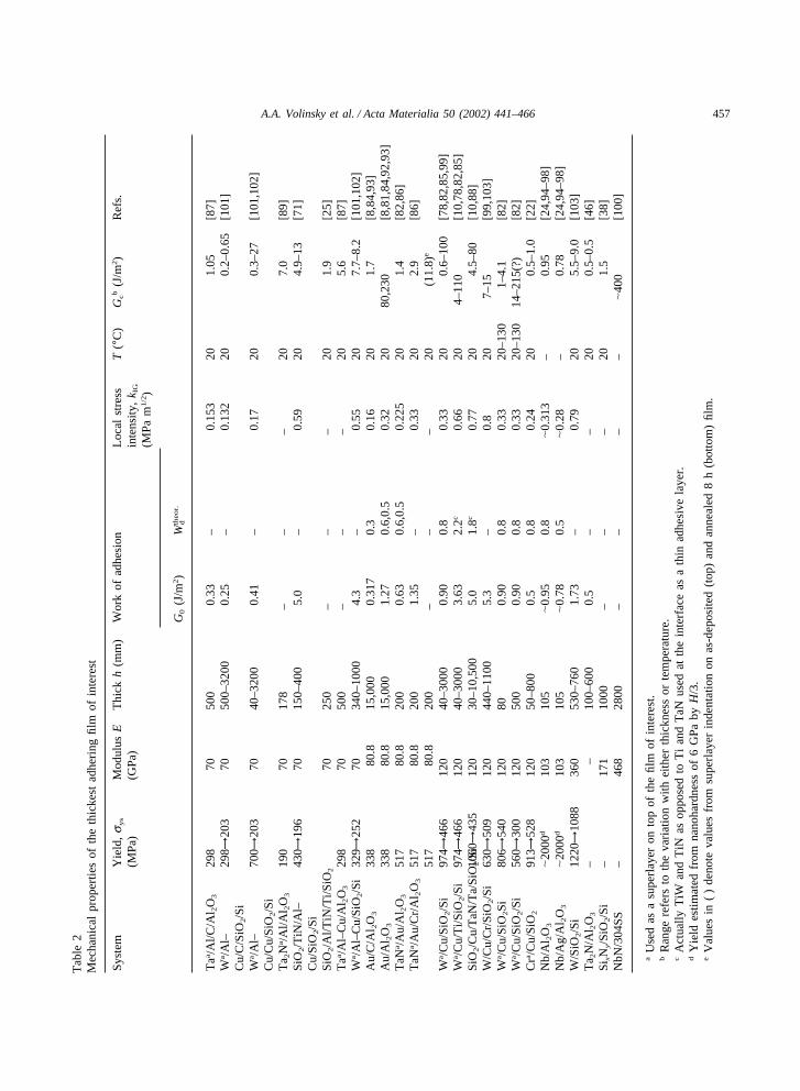
457A.A. Volinsky et al. / Acta Materialia 50 (2002) 441–466
Tab
le2
Mec
hani
cal
prop
ertie
sof
the
thic
kest
adhe
ring
film
ofin
tere
st
Syst
emY
ield
,s
ys
Mod
ulus
ET
hick
h(m
m)
Wor
kof
adhe
sion
Loc
alst
ress
T(°
C)
Gcb
(J/m
2)
Ref
s.(M
Pa)
(GPa
)in
tens
ity,
k IG
(MPa
m1/2
)
G0
(J/m
2)
Wth
eor.
d
Taa /A
l/C/A
l 2O
329
870
500
0.33
–0.
153
201.
05[8
7]W
a /A
l–29
8→20
370
500–
3200
0.25
–0.
132
200.
2–0.
65[1
01]
Cu/
C/S
iO2/S
iW
a /A
l–70
0→20
370
40–3
200
0.41
–0.
1720
0.3–
27[1
01,1
02]
Cu/
Cu/
SiO
2/S
iT
a 2N
a /A
l/Al 2
O3
190
7017
8–
––
207.
0[8
9]Si
O2/T
iN/A
l–43
0→19
670
150–
400
5.0
–0.
5920
4.9–
13[7
1]C
u/Si
O2/S
iSi
O2/A
l/TiN
/Ti/S
iO2
7025
0–
––
201.
9[2
5]T
aa /A
l–C
u/A
l 2O
329
870
500
––
–20
5.6
[87]
Wa /A
l–C
u/Si
O2/S
i32
9→25
270
340–
1000
4.3
–0.
5520
7.7–
8.2
[101
,102
]A
u/C
/Al 2
O3
338
80.8
15,0
000.
317
0.3
0.16
201.
7[8
,84,
93]
Au/
Al 2
O3
338
80.8
15,0
001.
270.
6,0.
50.
3220
80,2
30[8
,81,
84,9
2,93
]T
aNa /
Au/
Al 2
O3
517
80.8
200
0.63
0.6,
0.5
0.22
520
1.4
[82,
86]
TaN
a /A
u/C
r/A
l 2O
351
780
.820
01.
35–
0.33
202.
9[8
6]51
780
.820
0–
––
20(1
1.8)
e
Wa /
Cu/
SiO
2/S
i97
4→46
612
040
–300
00.
900.
80.
3320
0.6–
100
[78,
82,8
5,99
]W
a /C
u/T
i/SiO
2/S
i97
4→46
612
040
–300
03.
632.
2c0.
6620
4–11
0[1
0,78
,82,
85]
SiO
2/C
u/T
aN/T
a/Si
O2/S
i10
60→
435
120
30–1
0,50
05.
01.
8c0.
7720
4.5–
80[1
0,88
]W
/Cu/
Cr/
SiO
2/S
i63
0→50
912
044
0–11
005.
3–
0.8
207–
15[9
9,10
3]W
a /Cu/
SiO
2Si
806→
540
120
800.
900.
80.
3320
–130
1–4.
1[8
2]W
a /C
u/Si
O2/S
i56
0→30
012
050
00.
900.
80.
3320
–130
14–2
15(?
)[8
2]C
ra /C
u/Si
O2
913→
528
120
50–8
000.
50.
80.
2420
0.5–
1.0
[22]
Nb/
Al 2
O3
�20
00d
103
105
�0.
950.
8�
0.31
3–
0.95
[24,
94–9
8]N
b/A
g/A
l 2O
3�
2000
d10
310
5�
0.78
0.5
�0.
28–
0.78
[24,
94–9
8]W
/SiO
2/S
i12
20→
1088
360
530–
760
1.73
–0.
7920
5.5–
9.0
[103
]T
a 2N
/Al 2
O3
––
100–
600
0.5
––
200.
5–0.
5[4
6]Si
xNy/
SiO
2/S
i–
171
1000
––
–20
1.5
[38]
NbN
/304
SS–
468
2800
––
––
�40
0[1
00]
aU
sed
asa
supe
rlay
eron
top
ofth
efil
mof
inte
rest
.b
Ran
gere
fers
toth
eva
riat
ion
with
eith
erth
ickn
ess
orte
mpe
ratu
re.
cA
ctua
llyT
iWan
dT
iNas
oppo
sed
toT
ian
dT
aNus
edat
the
inte
rfac
eas
ath
inad
hesi
vela
yer.
dY
ield
estim
ated
from
nano
hard
ness
of6
GPa
byH
/3.
eV
alue
sin
()
deno
teva
lues
from
supe
rlay
erin
dent
atio
non
as-d
epos
ited
(top
)an
dan
neal
ed8
h(b
otto
m)
film
.
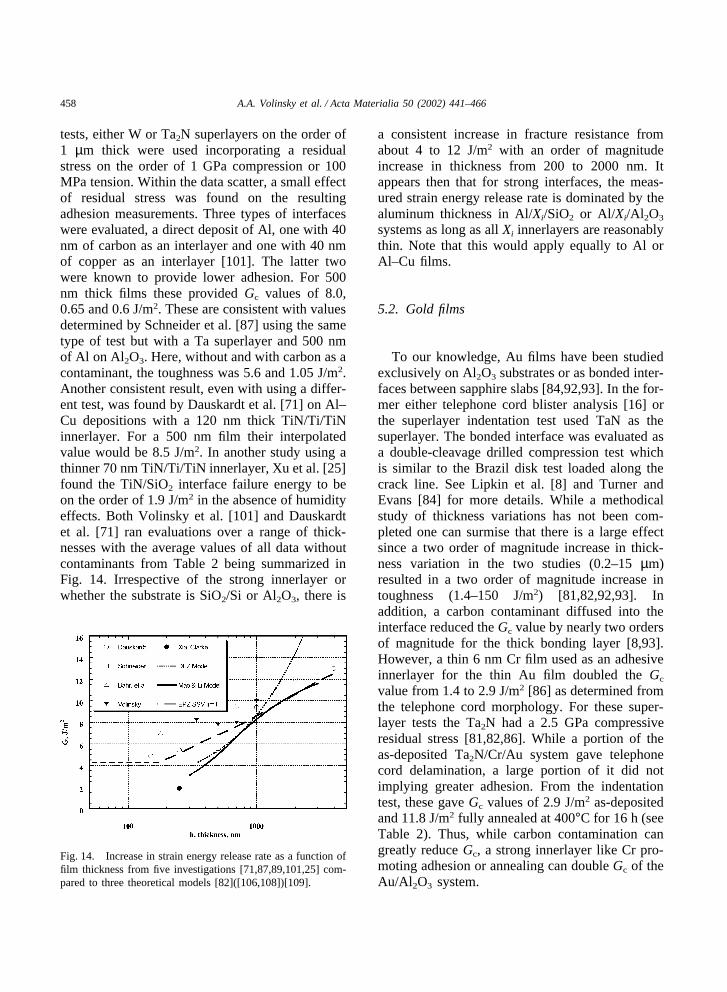
458 A.A. Volinsky et al. / Acta Materialia 50 (2002) 441–466
tests, either W or Ta2N superlayers on the order of1 µm thick were used incorporating a residualstress on the order of 1 GPa compression or 100MPa tension. Within the data scatter, a small effectof residual stress was found on the resultingadhesion measurements. Three types of interfaceswere evaluated, a direct deposit of Al, one with 40nm of carbon as an interlayer and one with 40 nmof copper as an interlayer [101]. The latter twowere known to provide lower adhesion. For 500nm thick films these provided Gc values of 8.0,0.65 and 0.6 J/m2. These are consistent with valuesdetermined by Schneider et al. [87] using the sametype of test but with a Ta superlayer and 500 nmof Al on Al2O3. Here, without and with carbon as acontaminant, the toughness was 5.6 and 1.05 J/m2.Another consistent result, even with using a differ-ent test, was found by Dauskardt et al. [71] on Al–Cu depositions with a 120 nm thick TiN/Ti/TiNinnerlayer. For a 500 nm film their interpolatedvalue would be 8.5 J/m2. In another study using athinner 70 nm TiN/Ti/TiN innerlayer, Xu et al. [25]found the TiN/SiO2 interface failure energy to beon the order of 1.9 J/m2 in the absence of humidityeffects. Both Volinsky et al. [101] and Dauskardtet al. [71] ran evaluations over a range of thick-nesses with the average values of all data withoutcontaminants from Table 2 being summarized inFig. 14. Irrespective of the strong innerlayer orwhether the substrate is SiO2/Si or Al2O3, there is
Fig. 14. Increase in strain energy release rate as a function offilm thickness from five investigations [71,87,89,101,25] com-pared to three theoretical models [82]([106,108])[109].
a consistent increase in fracture resistance fromabout 4 to 12 J/m2 with an order of magnitudeincrease in thickness from 200 to 2000 nm. Itappears then that for strong interfaces, the meas-ured strain energy release rate is dominated by thealuminum thickness in Al/Xi/SiO2 or Al/Xi/Al2O3
systems as long as all Xi innerlayers are reasonablythin. Note that this would apply equally to Al orAl–Cu films.
5.2. Gold films
To our knowledge, Au films have been studiedexclusively on Al2O3 substrates or as bonded inter-faces between sapphire slabs [84,92,93]. In the for-mer either telephone cord blister analysis [16] orthe superlayer indentation test used TaN as thesuperlayer. The bonded interface was evaluated asa double-cleavage drilled compression test whichis similar to the Brazil disk test loaded along thecrack line. See Lipkin et al. [8] and Turner andEvans [84] for more details. While a methodicalstudy of thickness variations has not been com-pleted one can surmise that there is a large effectsince a two order of magnitude increase in thick-ness variation in the two studies (0.2–15 µm)resulted in a two order of magnitude increase intoughness (1.4–150 J/m2) [81,82,92,93]. Inaddition, a carbon contaminant diffused into theinterface reduced the Gc value by nearly two ordersof magnitude for the thick bonding layer [8,93].However, a thin 6 nm Cr film used as an adhesiveinnerlayer for the thin Au film doubled the Gc
value from 1.4 to 2.9 J/m2 [86] as determined fromthe telephone cord morphology. For these super-layer tests the Ta2N had a 2.5 GPa compressiveresidual stress [81,82,86]. While a portion of theas-deposited Ta2N/Cr/Au system gave telephonecord delamination, a large portion of it did notimplying greater adhesion. From the indentationtest, these gave Gc values of 2.9 J/m2 as-depositedand 11.8 J/m2 fully annealed at 400°C for 16 h (seeTable 2). Thus, while carbon contamination cangreatly reduce Gc, a strong innerlayer like Cr pro-moting adhesion or annealing can double Gc of theAu/Al2O3 system.
459A.A. Volinsky et al. / Acta Materialia 50 (2002) 441–466
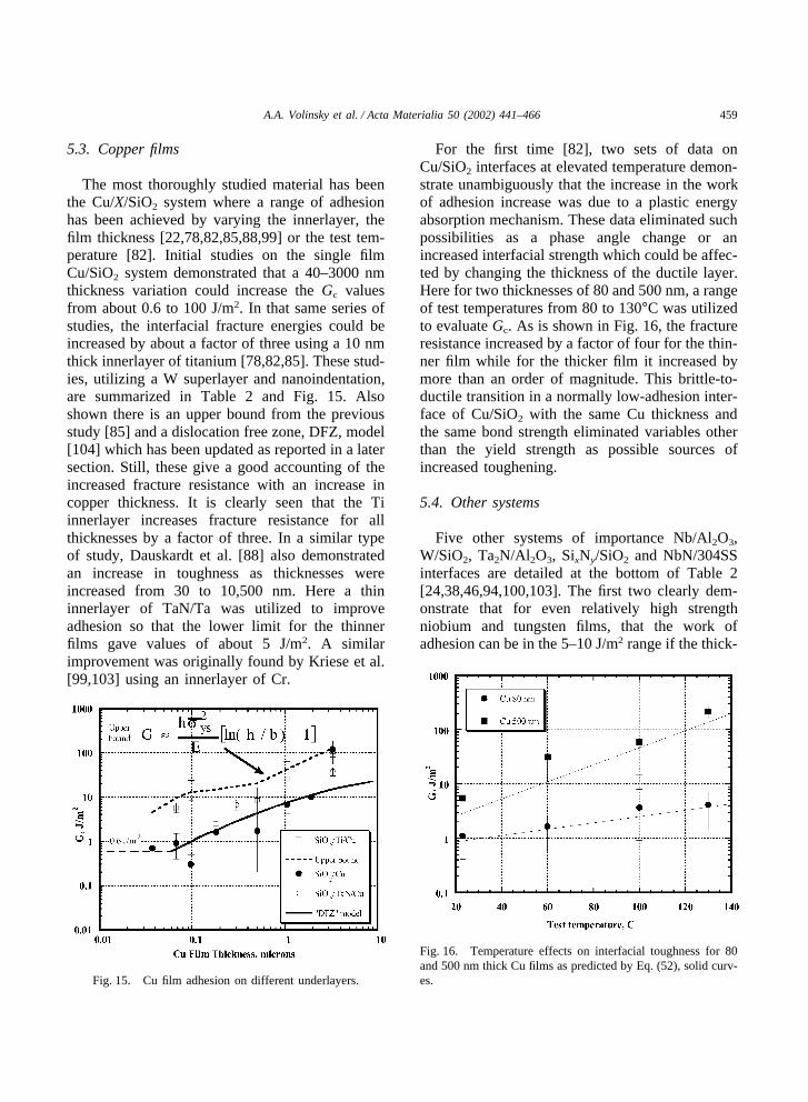
5.3. Copper films
The most thoroughly studied material has beenthe Cu/X/SiO2 system where a range of adhesionhas been achieved by varying the innerlayer, thefilm thickness [22,78,82,85,88,99] or the test tem-perature [82]. Initial studies on the single filmCu/SiO2 system demonstrated that a 40–3000 nmthickness variation could increase the Gc valuesfrom about 0.6 to 100 J/m2. In that same series ofstudies, the interfacial fracture energies could beincreased by about a factor of three using a 10 nmthick innerlayer of titanium [78,82,85]. These stud-ies, utilizing a W superlayer and nanoindentation,are summarized in Table 2 and Fig. 15. Alsoshown there is an upper bound from the previousstudy [85] and a dislocation free zone, DFZ, model[104] which has been updated as reported in a latersection. Still, these give a good accounting of theincreased fracture resistance with an increase incopper thickness. It is clearly seen that the Tiinnerlayer increases fracture resistance for allthicknesses by a factor of three. In a similar typeof study, Dauskardt et al. [88] also demonstratedan increase in toughness as thicknesses wereincreased from 30 to 10,500 nm. Here a thininnerlayer of TaN/Ta was utilized to improveadhesion so that the lower limit for the thinnerfilms gave values of about 5 J/m2. A similarimprovement was originally found by Kriese et al.[99,103] using an innerlayer of Cr.
Fig. 15. Cu film adhesion on different underlayers.
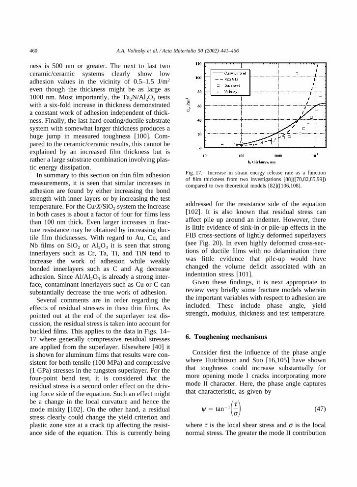
For the first time [82], two sets of data onCu/SiO2 interfaces at elevated temperature demon-strate unambiguously that the increase in the workof adhesion increase was due to a plastic energyabsorption mechanism. These data eliminated suchpossibilities as a phase angle change or anincreased interfacial strength which could be affec-ted by changing the thickness of the ductile layer.Here for two thicknesses of 80 and 500 nm, a rangeof test temperatures from 80 to 130°C was utilizedto evaluate Gc. As is shown in Fig. 16, the fractureresistance increased by a factor of four for the thin-ner film while for the thicker film it increased bymore than an order of magnitude. This brittle-to-ductile transition in a normally low-adhesion inter-face of Cu/SiO2 with the same Cu thickness andthe same bond strength eliminated variables otherthan the yield strength as possible sources ofincreased toughening.
5.4. Other systems
Five other systems of importance Nb/Al2O3,W/SiO2, Ta2N/Al2O3, SixNy/SiO2 and NbN/304SSinterfaces are detailed at the bottom of Table 2[24,38,46,94,100,103]. The first two clearly dem-onstrate that for even relatively high strengthniobium and tungsten films, that the work ofadhesion can be in the 5–10 J/m2 range if the thick-
Fig. 16. Temperature effects on interfacial toughness for 80and 500 nm thick Cu films as predicted by Eq. (52), solid curv-es.
460 A.A. Volinsky et al. / Acta Materialia 50 (2002) 441–466
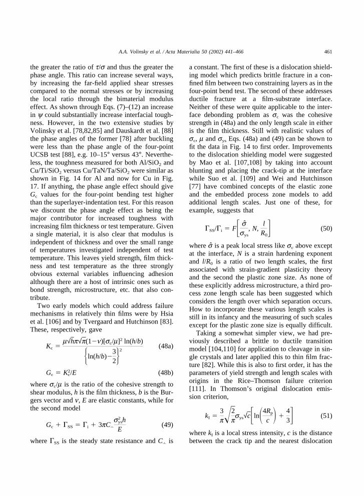
ness is 500 nm or greater. The next to last twoceramic/ceramic systems clearly show lowadhesion values in the vicinity of 0.5–1.5 J/m2
even though the thickness might be as large as1000 nm. Most importantly, the Ta2N/Al2O3 testswith a six-fold increase in thickness demonstrateda constant work of adhesion independent of thick-ness. Finally, the last hard coating/ductile substratesystem with somewhat larger thickness produces ahuge jump in measured toughness [100]. Com-pared to the ceramic/ceramic results, this cannot beexplained by an increased film thickness but israther a large substrate combination involving plas-tic energy dissipation.
In summary to this section on thin film adhesionmeasurements, it is seen that similar increases inadhesion are found by either increasing the bondstrength with inner layers or by increasing the testtemperature. For the Cu/X/SiO2 system the increasein both cases is about a factor of four for films lessthan 100 nm thick. Even larger increases in frac-ture resistance may be obtained by increasing duc-tile film thicknesses. With regard to Au, Cu, andNb films on SiO2 or Al2O3 it is seen that stronginnerlayers such as Cr, Ta, Ti, and TiN tend toincrease the work of adhesion while weaklybonded innerlayers such as C and Ag decreaseadhesion. Since Al/Al2O3 is already a strong inter-face, contaminant innerlayers such as Cu or C cansubstantially decrease the true work of adhesion.
Several comments are in order regarding theeffects of residual stresses in these thin films. Aspointed out at the end of the superlayer test dis-cussion, the residual stress is taken into account forbuckled films. This applies to the data in Figs. 14–17 where generally compressive residual stressesare applied from the superlayer. Elsewhere [40] itis shown for aluminum films that results were con-sistent for both tensile (100 MPa) and compressive(1 GPa) stresses in the tungsten superlayer. For thefour-point bend test, it is considered that theresidual stress is a second order effect on the driv-ing force side of the equation. Such an effect mightbe a change in the local curvature and hence themode mixity [102]. On the other hand, a residualstress clearly could change the yield criterion andplastic zone size at a crack tip affecting the resist-ance side of the equation. This is currently being
Fig. 17. Increase in strain energy release rate as a functionof film thickness from two investigations [88]([78,82,85,99])compared to two theoretical models [82]([106,108].
addressed for the resistance side of the equation[102]. It is also known that residual stress canaffect pile up around an indenter. However, thereis little evidence of sink-in or pile-up effects in theFIB cross-sections of lightly deformed superlayers(see Fig. 20). In even highly deformed cross-sec-tions of ductile films with no delamination therewas little evidence that pile-up would havechanged the volume deficit associated with anindentation stress [101].
Given these findings, it is next appropriate toreview very briefly some fracture models whereinthe important variables with respect to adhesion areincluded. These include phase angle, yieldstrength, modulus, thickness and test temperature.
6. Toughening mechanisms
Consider first the influence of the phase anglewhere Hutchinson and Suo [16,105] have shownthat toughness could increase substantially formore opening mode I cracks incorporating moremode II character. Here, the phase angle capturesthat characteristic, as given by
y � tan�1�ts� (47)
where t is the local shear stress and s is the localnormal stress. The greater the mode II contribution
461A.A. Volinsky et al. / Acta Materialia 50 (2002) 441–466
the greater the ratio of t/s and thus the greater thephase angle. This ratio can increase several ways,by increasing the far-field applied shear stressescompared to the normal stresses or by increasingthe local ratio through the bimaterial moduluseffect. As shown through Eqs. (7)–(12) an increasein y could substantially increase interfacial tough-ness. However, in the two extensive studies byVolinsky et al. [78,82,85] and Dauskardt et al. [88]the phase angles of the former [78] after bucklingwere less than the phase angle of the four-pointUCSB test [88], e.g. 10–15° versus 43°. Neverthe-less, the toughness measured for both Al/SiO2 andCu/Ti/SiO2 versus Cu/TaN/Ta/SiO2 were similar asshown in Fig. 14 for Al and now for Cu in Fig.17. If anything, the phase angle effect should giveGc values for the four-point bending test higherthan the superlayer-indentation test. For this reasonwe discount the phase angle effect as being themajor contributor for increased toughness withincreasing film thickness or test temperature. Givena single material, it is also clear that modulus isindependent of thickness and over the small rangeof temperatures investigated independent of testtemperature. This leaves yield strength, film thick-ness and test temperature as the three stronglyobvious external variables influencing adhesionalthough there are a host of intrinsic ones such asbond strength, microstructure, etc. that also con-tribute.
Two early models which could address failuremechanisms in relatively thin films were by Hsiaet al. [106] and by Tvergaard and Hutchinson [83].These, respectively, gave
Kc �m√hp√p(1�n)[sc/m]2 ln(h/b)
ln(h/b)�32�2
(48a)
Gc � K2c/E (48b)
where sc/m is the ratio of the cohesive strength toshear modulus, h is the film thickness, b is the Bur-gers vector and n, E are elastic constants, while forthe second model
Gc � �SS � �i � 3pC�
s2yshE
(49)
where �SS is the steady state resistance and C� is
a constant. The first of these is a dislocation shield-ing model which predicts brittle fracture in a con-fined film between two constraining layers as in thefour-point bend test. The second of these addressesductile fracture at a film-substrate interface.Neither of these were quite applicable to the inter-face debonding problem as sc was the cohesivestrength in (48a) and the only length scale in eitheris the film thickness. Still with realistic values ofsc, m and sys Eqs. (48a) and (49) can be shown tofit the data in Fig. 14 to first order. Improvementsto the dislocation shielding model were suggestedby Mao et al. [107,108] by taking into accountblunting and placing the crack-tip at the interfacewhile Suo et al. [109] and Wei and Hutchinson[77] have combined concepts of the elastic zoneand the embedded process zone models to addadditional length scales. Just one of these, forexample, suggests that
�SS/�i � F� ssys
, N,l
R0� (50)
where s is a peak local stress like sc above exceptat the interface, N is a strain hardening exponentand l/R0 is a ratio of two length scales, the firstassociated with strain-gradient plasticity theoryand the second the plastic zone size. As none ofthese explicitly address microstructure, a third pro-cess zone length scale has been suggested whichconsiders the length over which separation occurs.How to incorporate these various length scales isstill in its infancy and the measuring of such scalesexcept for the plastic zone size is equally difficult.
Taking a somewhat simpler view, we had pre-viously described a brittle to ductile transitionmodel [104,110] for application to cleavage in sin-gle crystals and later applied this to thin film frac-ture [82]. While this is also to first order, it has theparameters of yield strength and length scales withorigins in the Rice–Thomson failure criterion[111]. In Thomson’s original dislocation emis-sion criterion,
kI �3p�
2psys√c�ln�4Rp
c � �43� (51)
where kI is a local stress intensity, c is the distancebetween the crack tip and the nearest dislocation
462 A.A. Volinsky et al. / Acta Materialia 50 (2002) 441–466
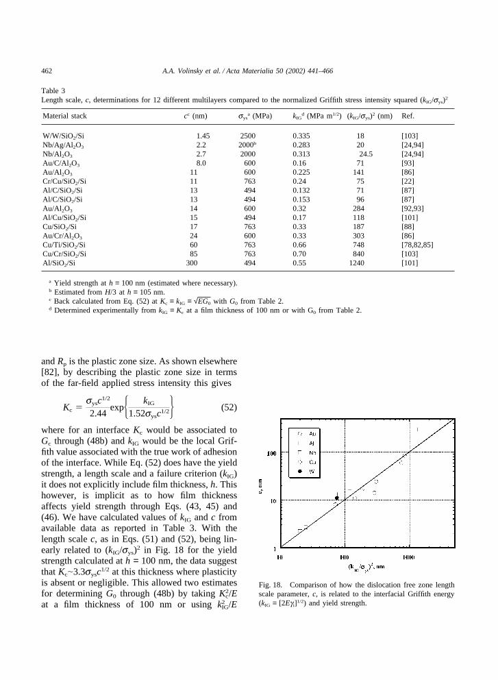
Table 3Length scale, c, determinations for 12 different multilayers compared to the normalized Griffith stress intensity squared (kIG/sys)2
Material stack cc (nm) sysa (MPa) kIG
d (MPa m1/2) (kIG/sys)2 (nm) Ref.
W/W/SiO2/Si 1.45 2500 0.335 18 [103]Nb/Ag/Al2O3 2.2 2000b 0.283 20 [24,94]Nb/Al2O3 2.7 2000 0.313 24.5 [24,94]Au/C/Al2O3 8.0 600 0.16 71 [93]Au/Al2O3 11 600 0.225 141 [86]Cr/Cu/SiO2/Si 11 763 0.24 75 [22]Al/C/SiO2/Si 13 494 0.132 71 [87]Al/C/SiO2/Si 13 494 0.153 96 [87]Au/Al2O3 14 600 0.32 284 [92,93]Al/Cu/SiO2/Si 15 494 0.17 118 [101]Cu/SiO2/Si 17 763 0.33 187 [88]Au/Cr/Al2O3 24 600 0.33 303 [86]Cu/Ti/SiO2/Si 60 763 0.66 748 [78,82,85]Cu/Cr/SiO2/Si 85 763 0.70 840 [103]Al/SiO2/Si 300 494 0.55 1240 [101]
a Yield strength at h = 100 nm (estimated where necessary).b Estimated from H/3 at h = 105 nm.c Back calculated from Eq. (52) at Kc = kIG = √EG0 with G0 from Table 2.d Determined experimentally from kIG = Kc at a film thickness of 100 nm or with G0 from Table 2.
and Rp is the plastic zone size. As shown elsewhere[82], by describing the plastic zone size in termsof the far-field applied stress intensity this gives
Kc �sysc1/2
2.44exp kIG
1.52sysc1/2� (52)
where for an interface Kc would be associated toGc through (48b) and kIG would be the local Grif-fith value associated with the true work of adhesionof the interface. While Eq. (52) does have the yieldstrength, a length scale and a failure criterion (kIG)it does not explicitly include film thickness, h. Thishowever, is implicit as to how film thicknessaffects yield strength through Eqs. (43, 45) and(46). We have calculated values of kIG and c fromavailable data as reported in Table 3. With thelength scale c, as in Eqs. (51) and (52), being lin-early related to (kIG/sys)2 in Fig. 18 for the yieldstrength calculated at h = 100 nm, the data suggestthat Kc�3.3sysc1/2 at this thickness where plasticityis absent or negligible. This allowed two estimatesfor determining G0 through (48b) by taking K2
c/Eat a film thickness of 100 nm or using k2
IG/E
Fig. 18. Comparison of how the dislocation free zone lengthscale parameter, c, is related to the interfacial Griffith energy(kIG = [2Egi]1/2) and yield strength.
463A.A. Volinsky et al. / Acta Materialia 50 (2002) 441–466
directly.1 As these were comparable, the latter areshown in Table 3. Where possible we comparedthese to the thermodynamic works of adhesion,Wad, as determined from high temperaturemeasurements [95–98] in Fig. 19. Except for tworelatively high and low points, the comparison isfavorable with G0 values only slightly higher thanthe thermodynamic adhesion values. Note that inTable 2 we have taken a few liberties in assumingthat a TiW interface (which is mostly titanium)with SiO2 is similar to a Ti/SiO2 interface and thatTaN/SiO2 would be similar to TiN/SiO2. Evenwithout these, however, the agreement is encour-aging.
To illustrate the predictive qualities of thesemodels, we have included a comparison of these tothe aluminum data of Fig. 14. Beyond the criticalthickness, G0 increases to Gc due to plastic energy
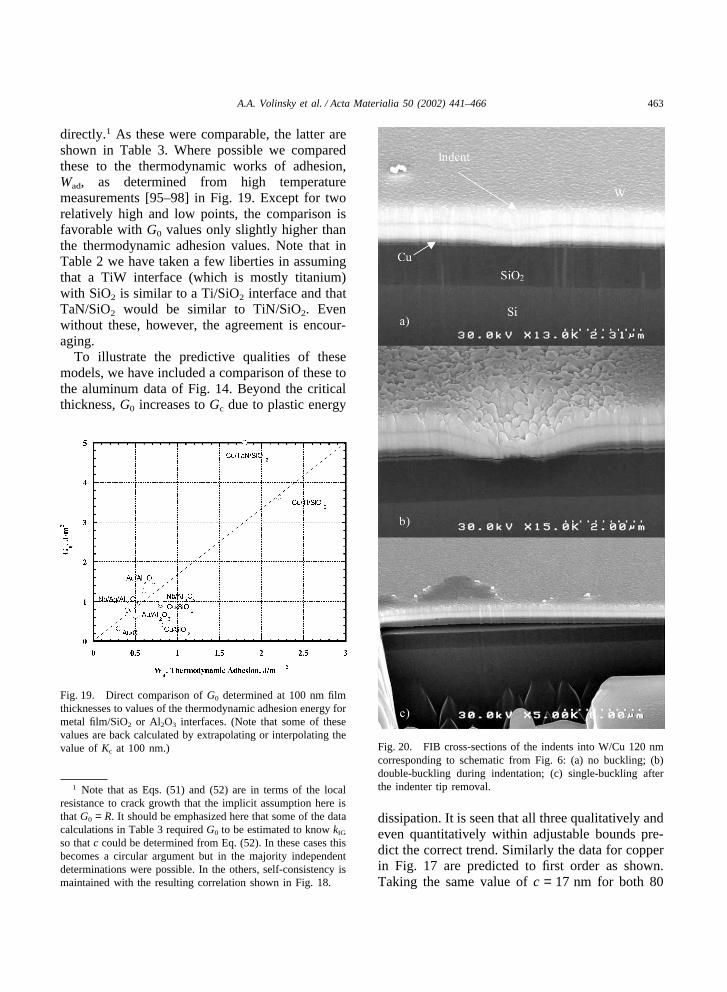
Fig. 19. Direct comparison of G0 determined at 100 nm filmthicknesses to values of the thermodynamic adhesion energy formetal film/SiO2 or Al2O3 interfaces. (Note that some of thesevalues are back calculated by extrapolating or interpolating thevalue of Kc at 100 nm.)
1 Note that as Eqs. (51) and (52) are in terms of the localresistance to crack growth that the implicit assumption here isthat G0 = R. It should be emphasized here that some of the datacalculations in Table 3 required G0 to be estimated to know kIG
so that c could be determined from Eq. (52). In these cases thisbecomes a circular argument but in the majority independentdeterminations were possible. In the others, self-consistency ismaintained with the resulting correlation shown in Fig. 18.
Fig. 20. FIB cross-sections of the indents into W/Cu 120 nmcorresponding to schematic from Fig. 6: (a) no buckling; (b)double-buckling during indentation; (c) single-buckling afterthe indenter tip removal.
dissipation. It is seen that all three qualitatively andeven quantitatively within adjustable bounds pre-dict the correct trend. Similarly the data for copperin Fig. 17 are predicted to first order as shown.Taking the same value of c = 17 nm for both 80
464 A.A. Volinsky et al. / Acta Materialia 50 (2002) 441–466
and 500 nm films as was used for Fig. 17, it isseen in Fig. 16 that the brittle-to-ductile transitioncan be predicted as a function of test temperature.The only variable used here was that of test tem-perature as to how it changed yield strength in Eq.(52). To summarize, this relatively simple three-parameter model with a single flow parameter, sys,a single failure criterion, kIG � √(EG0), and a sin-gle length scale, c, predict both the thickness andtemperature dependencies of Kc and therefore Gc,the practical work of adhesion.
One final point on these toughening mechanismsand models is that a length scale dependenceimplies a relationship between the measured frac-ture resistance and the thermodynamic work ofadhesion. Such models as embodied in elastic coremodels of Eq. (50) can lead to a power law depen-dence while those with a dislocation free zone likeEq. (52) can lead to an exponential dependence.To simplify, these can be expressed as
Gc
Wd
�� Wd
bsys�1�n
n;
Gc
Wd
�s2
yscEWd
exp�p3EWd
8s2ysc
�1/2�(53)
where the first comes from strain-gradient plas-ticity considerations [20] and the second fromdiscretized dislocation shielding [111] and Eq.(52). For a typical yield strength range of 400–1000 MPa with E, Wd and n being 200 GPa, 2 J/m2
and 0.2, one can show with c�80b, both of thesepredict large values of Gc/Wd on the order of sev-eral orders of magnitude. Furthermore, that ratioincreases by about a factor of 40 in the first caseand a factor of 80 in the second as yield strengthis decreased from 1000 to 400 MPa.
6.1. Note added in proof
After the experimental work associated withsuperlayer-indentation was completed and ana-lyzed, it came to our attention that FIB was avail-able. Several cross sections of Cu/SiO2 interfacesindented at low, intermediate and high loads wereevaluated [112]. As seen in Fig. 20(a), the inden-tation at low load did not trigger delamination. In20(b), a relatively large load plastically deformedthe tungsten and pinned the regions between thecrack right under the indenter and those extending
further out on both sides to produce the blister.There is about a 500 nm hiatus in cracking on bothsides of the central crack. Even though the filmwas only 120 nm thick, this resulted in a doublebuckling mode. Finally, in a third indent, it is seenin Fig. 3(c) that single buckling results. At thecenter of the original indent, it is now seen that thecrack opening is greatest. Compare these with theschematics shown in Fig. 6.
7. Summary
Some twelve thin film or interfacial adhesiontests are reviewed with emphasis toward ductile,thin metallic films. In addition 25 single and multi-film stacks on silicon or alumina substrates arereviewed as to how variations in thickness, chemis-try and temperature affect adhesion. Major rolesare shown for thickness, test temperature and inter-face chemistry as to how they affect yield strengthand the thermodynamic work of adhesion. For Al,Cu and Au films, any one of these variables areshown to change the practical work of adhesion byan order of magnitude or more. At low thickness,the adhesion asymptotically approaches the ther-modynamic work of adhesion while large thicknesspredominantly controls the practical work ofadhesion through plastic energy dissipation. It isshown that resistance-based models need yieldstrength, a failure criterion and at least one lengthscale for predictive quality.
Acknowledgements
The authors would like to acknowledge supportfor this work by the Center for Interfacial Engin-eering at the University of Minnesota under grantNSF/CDR-8721551 and the Department of Energyunder DOE contract DE-FG02/96ER45574. A.A.Volinsky and N.R. Moody also acknowledge sup-port through DOE contract DE-AC04-94AL85000.The assistance of N.I. Tymiak, B.E. Mills, D.E.McLean and D. Medlin is appreciated. The assist-ance of Dr. J.C. Nelson from the Center for Interfa-cial Engineering and Microtechnology Laboratorystaff at the University of Minnesota is also grate-
465A.A. Volinsky et al. / Acta Materialia 50 (2002) 441–466
fully appreciated. We would also like to thankIndira S. Adhihetty, Joseph B. Vella, Robert H.Carpenter and Lester Casoose Jr. of Motorola, Inc.for help with the FIB analysis.
References
[1] Steinmann PA, Hintermann HE. J Vac Sci Tech1989;A7:2267.
[2] Ohring M. The materials science of thin films. New York:Academic Press, 1991.
[3] Pocius A. Adhesion and adhesives technology. An intro-duction. New York: Hanser, 1997.
[4] Griffith AA. Phil Trans R Soc London 1920;A221:163.[5] Orowan E. Trans Isntn Engrs Shipbuilders Scot
1945;89:89.[6] Pilliar RM, Nutting J. Phil Mag 1967;16:181.[7] Reimanis I, Dalgleish BJ, Ruhle M, Evans AG. Acta Met-
all 1990;38:2645.[8] Lipkin DM, Clarke DR, Evans AG. Acta Mater
1998;46:4835.[9] Lee C, Lin K. Japan J Appl Phys 1994;33:2684.
[10] Furuya A, Hosoi N, Ohshita Y. J Appl Phys 1995;78:5989.[11] Jokl ML, Vitek V, McMahon CJ. Acta Metall
1980;28:1479.[12] Liechti KM, Chai YS. J Appl Mech 1992;59:295.[13] Cao HC, Evans AG. Mech Mater 1989;7:295.[14] Wang JS, Suo Z. Acta Metall Mater 1990;38:1279.[15] Jensen HM, Thouless MD. Int J Solids Struct
1993;30:779.[16] Hutchinson J, Suo Z. Adv Appl Mech 1992;29:63.[17] Dundurs J. J Appl Mech 1965;32:400.[18] Rice JR. In: Yokobori T, Kawasaki T, Swedlow JL, edi-
tors. Proceedings of the 1st International Conference onFracture, Sendai, Japan, 1966:309.
[19] Lipkin DM, Beltz GE. Acta Mater 1996;44:1287.[20] Lipkin DM, Clarke DR, Beltz GE. Acta Mater
1996;44:4051.[21] Bagchi A, Lucas G, Suo Z, Evans A. J Mater Res
1994;9:1734.[22] Bagchi A, Evans A. MRS Symp. Proc. 1995;383:183;
Bagchi A, Evans A. Thin Solid Films 1996;286:203.[23] Kinbara A, Kusano E, Kamiya T, Kondo I, Takenaka O.
Thin Solid Films 1998;317:165.[24] Ji H, Was GS, Thouless MD. Engng Fract Mech
1998;61:163.[25] Xu G, He M-Y, Clarke DR. Acta Mater 1999;47:4113.[26] Zhuk AV, Evans AG, Hutchinson JW. J Mater Res
1998;13:3555.[27] Oliver WC, Pharr GM. J Mater Res 1992;7:1564.[28] Evans AG, Hutchinson JW. Int J Solids Struct
1984;20(5):455.[29] Marshall DB, Evans AG. J Appl Phys 1984;56:2632.[30] Rosenfeld LG, Ritter JE, Lardner TJ, Lin MR. J Appl
Phys 1990;67:3291.
[31] de Boer MP, Gerberich WW. Acta Mater 1996;44:3169.[32] de Boer MP, Gerberich WW. Acta Mater 1996;44:3177.[33] de Boer MP. PhD dissertation, University of Minnesota,
1996.[34] Vlassak JJ, Drory MD, Nix WD. J Mater Res
1997;12:1900.[35] Drory MD, Hutchinson JW. Proc R Soc London
1996;A452:2319.[36] Volinsky AA, Nelson JC, Gerberich WW. Mater Res Soc
Proc 1999;563:397.[37] Begley MR, Mumm DR, Evans AG, Hutchinson JW. Acta
Mater 2000;48:3211.[38] Sanchez JM, El-Mansy S, Sun B, Scherban T, Fang N,
Pantuso D, Ford W, Elizalde MR, Martinez-Escanola JM,Martin-Meizoso A, Gil-Sevillano J, Fuentes M, Maiz J.Acta Mater 1999;4:4405.
[39] Kriese MD, Gerberich WW. J Mater Res 1999;14:3007.[40] Volinsky AA, Moody NR, Gerberich WW. Mater Res Soc
Proc 2000;594:383.[41] Timoshenko SP. Theory of elastic stability. New York:
McGraw-Hill, 1961.[42] Benjamin P, Weaver C. Proc R Soc London
1960;A254:163.[43] Burnett P, Rickersby D. Thin Solid Films 1987;154:403.[44] Venkataraman S, Kohlstedt D, Gerberich WW. J Mater
Res 1993;8:685.[45] Venkataraman S, Kohlstedt D, Gerberich WW. J Mater
Res 1992;7:1126.[46] Moody NR, Hwang R, Venkataraman S, Angelo J, Nor-
wood D, Gerberich WW. Acta Mater 1998;46:585.[47] de Boer MP, Kriese M, Gerberich WW. J Mater Res
1997;12:2673.[48] de Boer MP, Nelson JC, Gerberich WW. J Mater Res
1998;13:1002.[49] Vlassak J, Nix W. J Mater Res 1992;7:3242.[50] Small MK, Vlassak J, Nix W. MRS Symp Proc
1992;239:257.[51] Small MK, Nix WD. J Mater Res 1992;7:1553.[52] Paviot V, Vlassak J, Nix W. MRS Symp Proc
1995;356:579.[53] Hohfelder R, Luo H, Vlassak J, Chidsey C, Nix W. MRS
Symp Proc 1997;436:115.[54] Volinsky AA. Unpublished work.[55] Wan K-T, Lim S-C. Int J Fract 1998;92:43.[56] Jensen HM. Int J Fract 1998;94:79.[57] ASTM Standard 399-90 1990:407.[58] Suo Z, Hutchinson JW. Mater Sci Engng 1989;A107:135.[59] Menningen M, Weiss H. Surf Coatings Tech 1995;76-
77:835.[60] McNaney JM, Havens R, Ritchie RO. J Test Eval
1995;23:28.[61] McNaney JM, M Cannon R, Ritchie RO. J Test Eval
1995;23:95.[62] Kanninen MF. Int J Fract 1973;9:83.[63] Cao HC, Dalgleish BJ, Evans AG. Closed Loop
1989;17:19.
466 A.A. Volinsky et al. / Acta Materialia 50 (2002) 441–466
[64] O’Dowd N, Shih C, Stout M. Int J Solids Struct1992;29:571.
[65] Atkinson C, Smelser R, Sanchez J. Int J Fract1982;18(4):279.
[66] Shetty D, Rosenfield A, Duckworth W. Engng FractMech 1987;26(6):825.
[67] Huang Y, Liu C, Stout MG. Acta Mater 1996;44:1223.[68] Wang J, Suo Z. Acta Metall Mater 1990;38:1279.[69] Charalambides G, Lund J, Evans AG, McMeeking RM. J
Appl Mech 1989;111:77.[70] Hofinger I, Oechsner M, Bahr H, Swain M. Int J Fract
1998;92:213.[71] Dauskardt RH, Lane M, Ma Q, Krishna N. Engng Fract
Mech 1998;61:141.[72] Becker Jr. TL, McNaney JM, Cannon RM, Ritchie RO.
Mech Mater 1997;25:291.[73] Weihs TP, Hong S, Bravman JC, Nix WD. J Mater Res
1988;3:931.[74] Baker SP, Nix WD. J Mater Res 1994;9:3131.[75] Baker SP, Nix WD. J Mater Res 1994;9:3145.[76] Kramer D, Huang H, Kriese M, Robach J, Nelson J,
Wright A, Bahr D, Gerberich WW. Acta Mater1999;47:333.
[77] Wei Y, Hutchinson JW. J Mech Phys Solids1997;45:1137.
[78] Tymiak N, Volinsky AA, Kriese MD, Downs SA, Gerber-ich WW. Met Mater Trans A 2000;31A:863.
[79] Vinci RP, Ziplinski EM, Bravman JC. Thin Solid Films1995;262:142.
[80] Venkataraman R, Bravman JC. J Mater Res 1992;7:2040.[81] Evans AG, Hutchinson JW, Wei Y. Acta Mater
1999;47:4093.[82] Gerberich WW, Volinsky AA, Tymiak NI, Moody NR.
Mater Res Soc Proc 2000;594:351.[83] Tvergaard V, Hutchinson JW. J Mech Phys Solids
1996;44:789.[84] Turner MR, Evans AG. Acta Mater 1996;44:863.[85] Volinsky AA, Tymiak NI, Kriese MD, Gerberich WW,
Hutchinson JW. MRS Symp 1999;539:277.[86] Moody NR, Adams DP, Volinsky AA, Kriese MD, Ger-
berich WW. Mater Res Soc Proc 2000;586:195.[87] Schneider JA, Guthrie SE, Kriese MD, Clift WM, Moody
NR. Mat Res Soc Symp 1998;522:347.[88] Lane M, Dauskardt RH. J Mater Res 2000;15:203.[89] Bahr DF, Hoehn JW, Moody NR, Gerberich WW. Acta
Mater 1997;45:5163.
[90] Moody NR, Venkataraman SK, Hwang RQ, Angelo JE,Gerberich WW. In: Magnin T, editor.Corrosion/deformation interactions. Eur Fed Corros Publ21, 1997. p. 227.
[91] Lane M, Vainchtein A, Gao H, Dauskardt RH. J MaterRes 2000;15(12):22758–69.
[92] Reimanis IE. Acta Mater 1998;46:2479.[93] Lipkin DM, Clarke DR, Evans AG. Acta Mater
1998;46:4835.[94] Ji H, Was GS, Thouless MD. Mat Res Soc Symp
1998;522:325.[95] Nicholas MG. In: Dufour LC, editor. Surfaces and inter-
faces of ceramic materials, Norwell, MA: Kluwer Aca-demic Press; 1989:393.
[96] Hondros ED. In: Precipitation processes in solids. Warren-dale (PA): TMS-AIME; 1978. p. 1.
[97] Pilliar RM, Nutting J. Philos Mag 1967;16:181.[98] Smialek JL, Jayne DT, Schaeffer JC, Murphy WH. Thin
Solid Films 1994;253:285.[99] Kriese MD, Moody NR, Gerberich WW. Acta Mater
1998;46:6623.[100] Hainsworth SV, McGurk MR, Page TF. Surfaces and
Coatings Technology 1998;102:97.[101] Gerberich WW, Volinsky AA, Tymiak NI, Moody NR.
Mater Res Soc Proc 594;2000:383; Volinsky AA. PhDthesis, University of Minnesota, 2000.
[102] Dauskardt RH. Private communication, Stanford Univer-sity, 2001.
[103] Kriese MD, Moody NR, Gerberich WW. J Mater Res1999;14:3019.
[104] Zielinski W, Huang H, Marsh PG, and Gerberich WW.Part I, II, III. Acta Metall Mater 40;1992:2861, 2873,2883.
[105] Suo Z, Hutchinson J. Int J Fract 1990;43:1.[106] Hsia KJ, Suo Z, Yang W. J Mech Phys Solids
1994;42:877.[107] Mao SX, Li X-P. Philos Mag A 1999;79(8):1817.[108] Mao SX, Li MZ. J Mech Phys Solids 1999;47:2351.[109] Suo Z, Shih F, Varias A. Acta Metall Mater
1993;41:1551.[110] Huang H, Gerberich WW. Acta Metall Mater
42;1994:639; Marsh PG, Gerberich WW. Acta MetallMater 42;1994:613.
[111] Rice JR, Thomson R. Philos Mag 1974;29:73.[112] Volinsky AA, Kottke ML, Adhihetty IS, Gerberich WW.
Fiducial marks as a measure of thin film crack arresttoughness. Invited paper, ICF10, December 2001.