ICM-20608-G Register Maps and Description Revision 1
23
ICM-20608-G InvenSense reserves the right to change the detail specifications as may be required to permit improvements in the design of its products. InvenSense Inc. 1745 Technology Drive, San Jose, CA 95110 U.S.A +1(408) 988–7339 www.invensense.com Document Number: RM-000030 Rev Number: 1.0 Rev Date: 06/15/2015 ICM-20608-G Register Maps and Description Revision 1.0
Transcript of ICM-20608-G Register Maps and Description Revision 1
ICM-20608-G
InvenSense reserves the right to change the detail specifications as may be required to permit improvements in the design of its products.
InvenSense Inc. 1745 Technology Drive, San Jose, CA 95110 U.S.A
+1(408) 988–7339 www.invensense.com
Document Number: RM-000030 Rev Number: 1.0 Rev Date: 06/15/2015
ICM-20608-G Register Maps and Description Revision 1.0
ICM-20608-G
Page 2 of 23 Document Number: RM-000030 Revision: 1.0
1 Purpose and Scope .............................................................................................................................................. 3
2 Register Map ........................................................................................................................................................ 4
3 Register Descriptions ........................................................................................................................................... 6
3.1 Registers 0 to 2 – Gyroscope Self-Test Registers ...................................................................................... 6
3.2 Registers 13 to 15 – Accelerometer Self-Test Registers ............................................................................ 6
3.3 Registers 19 – Gyro Offset Adjustment Register ....................................................................................... 7
3.1 Registers 20 – Gyro Offset Adjustment Register ....................................................................................... 7
3.2 Registers 21 – Gyro Offset Adjustment Register ....................................................................................... 7
3.3 Registers 22 – Gyro Offset Adjustment Register ....................................................................................... 7
3.4 Registers 23 – Gyro Offset Adjustment Register ....................................................................................... 8
3.5 Register 24 – Gyro Offset Adjustment Register ........................................................................................ 8
3.6 Register 25 – Sample Rate Divider ............................................................................................................ 8
3.7 Register 26 – Configuration....................................................................................................................... 9
3.8 Register 27 – Gyroscope Configuration .................................................................................................... 9
3.9 Register 28 – Accelerometer Configuration ............................................................................................ 10
3.10 Register 29 – Accelerometer Configuration 2..................................................................................... 10
3.11 Register 30 – Low Power Mode Configuration ................................................................................... 11
3.12 Register 31 – Wake-on Motion Threshold (Accelerometer) ............................................................... 13
3.13 Register 35 – FIFO Enable ................................................................................................................... 14
3.14 Register 54 – FSYNC Interrupt Status.................................................................................................. 14
3.15 Register 55 – INT/DRDY Pin / Bypass Enable Configuration ............................................................... 14
3.16 Register 56 – Interrupt Enable ............................................................................................................ 15
3.17 Register 58 – Interrupt Status ............................................................................................................. 15
3.18 Registers 59 to 64 – Accelerometer Measurements .......................................................................... 16
3.19 Registers 65 and 66 – Temperature Measurement ............................................................................ 16
3.20 Registers 67 to 72 – Gyroscope Measurements ................................................................................. 17
3.21 Register 104 – Signal Path Reset ......................................................................................................... 18
3.22 Register 105 – Accelerometer Intelligence Control ............................................................................ 18
3.23 Register 106 – User Control ................................................................................................................ 19
3.24 Register 107 – Power Management 1 ................................................................................................ 19
3.25 Register 108 – Power Management 2 ................................................................................................ 20
3.26 Register 114 and 115 – FIFO Count Registers ..................................................................................... 20
3.27 Register 116 – FIFO Read Write .......................................................................................................... 21
3.28 Register 117 – Who Am I .................................................................................................................... 21
3.29 Registers 119, 120, 122, 123, 125, 126 Accelerometer Offset Registers ............................................ 21
4 Revision History ................................................................................................................................................. 23

ICM-20608-G
Page 3 of 23 Document Number: RM-000030 Revision: 1.0
1 PURPOSE AND SCOPE This document provides information regarding the register map and descriptions for the ICM-20608-G™. This document should be used in conjunction with the ICM-20608-G Product Specification (PS-ICM-20608-G-00) for detailed features, specifications, and other product information.
ICM-20608-G
Page 4 of 23 Document Number: RM-000030 Revision: 1.0
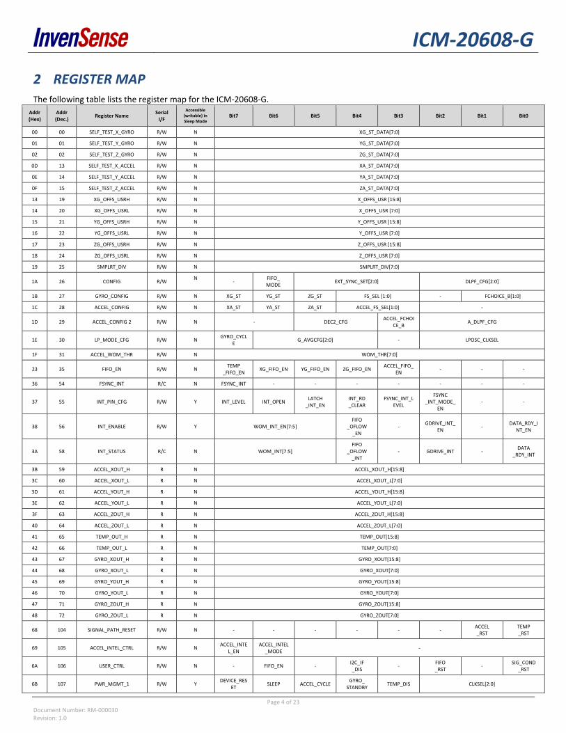
2 REGISTER MAP The following table lists the register map for the ICM-20608-G.
Addr (Hex)
Addr (Dec.)
Register Name Serial
I/F
Accessible (writable) in Sleep Mode
Bit7 Bit6 Bit5 Bit4 Bit3 Bit2 Bit1 Bit0
00 00 SELF_TEST_X_GYRO R/W N XG_ST_DATA[7:0]
01 01 SELF_TEST_Y_GYRO R/W N YG_ST_DATA[7:0]
02 02 SELF_TEST_Z_GYRO R/W N ZG_ST_DATA[7:0]
0D 13 SELF_TEST_X_ACCEL R/W N XA_ST_DATA[7:0]
0E 14 SELF_TEST_Y_ACCEL R/W N YA_ST_DATA[7:0]
0F 15 SELF_TEST_Z_ACCEL R/W N ZA_ST_DATA[7:0]
13 19 XG_OFFS_USRH R/W N X_OFFS_USR [15:8]
14 20 XG_OFFS_USRL R/W N X_OFFS_USR [7:0]
15 21 YG_OFFS_USRH R/W N Y_OFFS_USR [15:8]
16 22 YG_OFFS_USRL R/W N Y_OFFS_USR [7:0]
17 23 ZG_OFFS_USRH R/W N Z_OFFS_USR [15:8]
18 24 ZG_OFFS_USRL R/W N Z_OFFS_USR [7:0]
19 25 SMPLRT_DIV R/W N SMPLRT_DIV[7:0]
1A 26 CONFIG R/W N
- FIFO_ MODE
EXT_SYNC_SET[2:0] DLPF_CFG[2:0]
1B 27 GYRO_CONFIG R/W N XG_ST YG_ST ZG_ST FS_SEL [1:0] - FCHOICE_B[1:0]
1C 28 ACCEL_CONFIG R/W N XA_ST YA_ST ZA_ST ACCEL_FS_SEL[1:0] -
1D 29 ACCEL_CONFIG 2 R/W N - DEC2_CFG ACCEL_FCHOI
CE_B A_DLPF_CFG
1E 30 LP_MODE_CFG R/W N GYRO_CYCL
E G_AVGCFG[2:0] - LPOSC_CLKSEL
1F 31 ACCEL_WOM_THR R/W N WOM_THR[7:0]
23 35 FIFO_EN R/W N TEMP
_FIFO_EN XG_FIFO_EN YG_FIFO_EN ZG_FIFO_EN
ACCEL_FIFO_EN
- - -
36 54 FSYNC_INT R/C N FSYNC_INT - - - - - - -
37 55 INT_PIN_CFG R/W Y INT_LEVEL INT_OPEN LATCH
_INT_EN INT_RD _CLEAR
FSYNC_INT_LEVEL
FSYNC _INT_MODE_
EN - -
38 56 INT_ENABLE R/W Y WOM_INT_EN[7:5] FIFO
_OFLOW _EN
- GDRIVE_INT_
EN -
DATA_RDY_INT_EN
3A 58 INT_STATUS R/C N WOM_INT[7:5] FIFO
_OFLOW _INT
- GDRIVE_INT - DATA
_RDY_INT
3B 59 ACCEL_XOUT_H R N ACCEL_XOUT_H[15:8]
3C 60 ACCEL_XOUT_L R N ACCEL_XOUT_L[7:0]
3D 61 ACCEL_YOUT_H R N ACCEL_YOUT_H[15:8]
3E 62 ACCEL_YOUT_L R N ACCEL_YOUT_L[7:0]
3F 63 ACCEL_ZOUT_H R N ACCEL_ZOUT_H[15:8]
40 64 ACCEL_ZOUT_L R N ACCEL_ZOUT_L[7:0]
41 65 TEMP_OUT_H R N TEMP_OUT[15:8]
42 66 TEMP_OUT_L R N TEMP_OUT[7:0]
43 67 GYRO_XOUT_H R N GYRO_XOUT[15:8]
44 68 GYRO_XOUT_L R N GYRO_XOUT[7:0]
45 69 GYRO_YOUT_H R N GYRO_YOUT[15:8]
46 70 GYRO_YOUT_L R N GYRO_YOUT[7:0]
47 71 GYRO_ZOUT_H R N GYRO_ZOUT[15:8]
48 72 GYRO_ZOUT_L R N GYRO_ZOUT[7:0]
68 104 SIGNAL_PATH_RESET R/W N - - - - - - ACCEL _RST
TEMP _RST
69 105 ACCEL_INTEL_CTRL R/W N ACCEL_INTE
L_EN ACCEL_INTEL
_MODE -
6A 106 USER_CTRL R/W N - FIFO_EN - I2C_IF _DIS
- FIFO _RST
- SIG_COND
_RST
6B 107 PWR_MGMT_1 R/W Y DEVICE_RES
ET SLEEP ACCEL_CYCLE
GYRO_ STANDBY
TEMP_DIS CLKSEL[2:0]

ICM-20608-G
Page 5 of 23 Document Number: RM-000030 Revision: 1.0
Addr (Hex)
Addr (Dec.)
Register Name Serial
I/F
Accessible (writable) in Sleep Mode
Bit7 Bit6 Bit5 Bit4 Bit3 Bit2 Bit1 Bit0
6C 108 PWR_MGMT_2 R/W Y FIFO_LP_EN - STBY_XA STBY_YA STBY_ZA STBY_XG STBY_YG STBY_ZG
72 114 FIFO_COUNTH R N - FIFO_COUNT[12:8]
73 115 FIFO_COUNTL R N FIFO_COUNT[7:0]
74 116 FIFO_R_W R/W N FIFO_DATA[7:0]
75 117 WHO_AM_I R N WHOAMI[7:0]
77 119 XA_OFFSET_H R/W N XA_OFFS [14:7]
78 120 XA_OFFSET_L R/W N XA_OFFS [6:0] -
7A 122 YA_OFFSET_H R/W N YA_OFFS [14:7]
7B 123 YA_OFFSET_L R/W N YA_OFFS [6:0] -
7D 125 ZA_OFFSET_H R/W N ZA_OFFS [14:7]
7E 126 ZA_OFFSET_L R/W N ZA_OFFS [6:0] -
Note: Register Names ending in _H and _L contain the high and low bytes, respectively, of an internal register value. In the detailed register tables that follow, register names are in capital letters, while register values are in capital letters and italicized. For example, the ACCEL_XOUT_H register (Register 59) contains the 8 most significant bits, ACCEL_XOUT[15:8], of the 16-bit X-Axis accelerometer measurement, ACCEL_XOUT. The reset value is 0x00 for all registers other than the registers below, also the self-test registers contain pre-programmed values and will not be 0x00 after reset.
Register 107 (0x40) Power Management 1
Register 117 (0xAF) WHO_AM_I
ICM-20608-G
Page 6 of 23 Document Number: RM-000030 Revision: 1.0
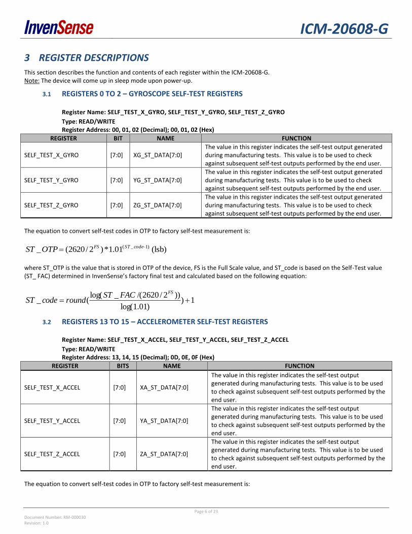
3 REGISTER DESCRIPTIONS This section describes the function and contents of each register within the ICM-20608-G. Note: The device will come up in sleep mode upon power-up.
3.1 REGISTERS 0 TO 2 – GYROSCOPE SELF-TEST REGISTERS
Register Name: SELF_TEST_X_GYRO, SELF_TEST_Y_GYRO, SELF_TEST_Z_GYRO
Type: READ/WRITE Register Address: 00, 01, 02 (Decimal); 00, 01, 02 (Hex)
REGISTER BIT NAME FUNCTION
SELF_TEST_X_GYRO [7:0] XG_ST_DATA[7:0] The value in this register indicates the self-test output generated during manufacturing tests. This value is to be used to check against subsequent self-test outputs performed by the end user.
SELF_TEST_Y_GYRO [7:0] YG_ST_DATA[7:0] The value in this register indicates the self-test output generated during manufacturing tests. This value is to be used to check against subsequent self-test outputs performed by the end user.
SELF_TEST_Z_GYRO [7:0] ZG_ST_DATA[7:0] The value in this register indicates the self-test output generated during manufacturing tests. This value is to be used to check against subsequent self-test outputs performed by the end user.
The equation to convert self-test codes in OTP to factory self-test measurement is:
(lsb) 01.1*)2/2620(_ )1_( codeSTFSOTPST
where ST_OTP is the value that is stored in OTP of the device, FS is the Full Scale value, and ST_code is based on the Self-Test value (ST_ FAC) determined in InvenSense’s factory final test and calculated based on the following equation:
1))01.1log(
))2/2620/(_log((_
FSFACSTroundcodeST
3.2 REGISTERS 13 TO 15 – ACCELEROMETER SELF-TEST REGISTERS
Register Name: SELF_TEST_X_ACCEL, SELF_TEST_Y_ACCEL, SELF_TEST_Z_ACCEL
Type: READ/WRITE Register Address: 13, 14, 15 (Decimal); 0D, 0E, 0F (Hex)
REGISTER BITS NAME FUNCTION
SELF_TEST_X_ACCEL [7:0] XA_ST_DATA[7:0]
The value in this register indicates the self-test output generated during manufacturing tests. This value is to be used to check against subsequent self-test outputs performed by the end user.
SELF_TEST_Y_ACCEL [7:0] YA_ST_DATA[7:0]
The value in this register indicates the self-test output generated during manufacturing tests. This value is to be used to check against subsequent self-test outputs performed by the end user.
SELF_TEST_Z_ACCEL [7:0] ZA_ST_DATA[7:0]
The value in this register indicates the self-test output generated during manufacturing tests. This value is to be used to check against subsequent self-test outputs performed by the end user.
The equation to convert self-test codes in OTP to factory self-test measurement is:

ICM-20608-G
Page 7 of 23 Document Number: RM-000030 Revision: 1.0
(lsb) 01.1*)2/2620(_ )1_( codeSTFSOTPST where ST_OTP is the value that is stored in OTP of the device, FS is the Full Scale value, and ST_code is based on the Self-Test value (ST_ FAC) determined in InvenSense’s factory final test and calculated based on the following equation:
1))01.1log(
))2/2620/(_log((_
FSFACSTroundcodeST
3.3 REGISTERS 19 – GYRO OFFSET ADJUSTMENT REGISTER
Register Name: XG_OFFS_USRH Register Type: READ/WRITE Register Address: 19 (Decimal); 13 (Hex)
BIT NAME FUNCTION
[7:0] X_OFFS_USR[15:8]
Bits 15 to 8 of the 16-bit offset of X gyroscope (2’s complement). This register is used to remove DC bias from the sensor output. The value in this register is added to the gyroscope sensor value before going into the sensor register.
3.1 REGISTERS 20 – GYRO OFFSET ADJUSTMENT REGISTER
Register Name: XG_OFFS_USRL Register Type: READ/WRITE Register Address: 20 (Decimal); 14 (Hex)
BIT NAME FUNCTION
[7:0] X_OFFS_USR[7:0]
Bits 7 to 0 of the 16-bit offset of X gyroscope (2’s complement). This register is used to remove DC bias from the sensor output. The value in this register is added to the gyroscope sensor value before going into the sensor register.
3.2 REGISTERS 21 – GYRO OFFSET ADJUSTMENT REGISTER
Register Name: YG_OFFS_USRH Register Type: READ/WRITE Register Address: 21 (Decimal); 15 (Hex)
BIT NAME FUNCTION
[7:0] Y_OFFS_USR[15:8]
Bits 15 to 8 of the 16-bit offset of Y gyroscope (2’s complement). This register is used to remove DC bias from the sensor output. The value in this register is added to the gyroscope sensor value before going into the sensor register.
3.3 REGISTERS 22 – GYRO OFFSET ADJUSTMENT REGISTER
Register Name: YG_OFFS_USRL Register Type: READ/WRITE Register Address: 22 (Decimal); 16 (Hex)

ICM-20608-G
Page 8 of 23 Document Number: RM-000030 Revision: 1.0
BIT NAME FUNCTION
[7:0] Y_OFFS_USR[7:0]
Bits 7 to 0 of the 16-bit offset of Y gyroscope (2’s complement). This register is used to remove DC bias from the sensor output. The value in this register is added to the gyroscope sensor value before going into the sensor register.
3.4 REGISTERS 23 – GYRO OFFSET ADJUSTMENT REGISTER
Register Name: ZG_OFFS_USRH Register Type: READ/WRITE Register Address: 23 (Decimal); 17 (Hex)
BIT NAME FUNCTION
[7:0] Z_OFFS_USR[15:8]
Bits 15 to 8 of the 16-bit offset of Z gyroscope (2’s complement). This register is used to remove DC bias from the sensor output. The value in this register is added to the gyroscope sensor value before going into the sensor register.
3.5 REGISTER 24 – GYRO OFFSET ADJUSTMENT REGISTER
Register Name: ZG_OFFS_USRL Register Type: READ/WRITE Register Address: 24 (Decimal); 18 (Hex)
BIT NAME FUNCTION
[7:0] Z_OFFS_USR[7:0]
Bits 7 to 0 of the 16-bit offset of Z gyroscope (2’s complement). This register is used to remove DC bias from the sensor output. The value in this register is added to the gyroscope sensor value before going into the sensor register.
3.6 REGISTER 25 – SAMPLE RATE DIVIDER
Register Name: SMPLRT_DIV Register Type: READ/WRITE Register Address: 25 (Decimal); 19 (Hex)
BIT NAME FUNCTION
[7:0] SMPLRT_DIV[7:0] Divides the internal sample rate (see register CONFIG) to generate the sample rate that controls sensor data output rate, FIFO sample rate. NOTE: This register is only effective when FCHOICE_B register bits are 2’b00, and (0 < DLPF_CFG < 7). This is the update rate of the sensor register: SAMPLE_RATE = INTERNAL_SAMPLE_RATE / (1 + SMPLRT_DIV) Where INTERNAL_SAMPLE_RATE = 1kHz

ICM-20608-G
Page 9 of 23 Document Number: RM-000030 Revision: 1.0
3.7 REGISTER 26 – CONFIGURATION Register Name: CONFIG Register Type: READ/WRITE Register Address: 26 (Decimal); 1A (Hex)
BIT NAME FUNCTION
[7] - Always set to 0
[6] FIFO_MODE When set to ‘1’, when the FIFO is full, additional writes will not be written to FIFO. When set to ‘0’, when the FIFO is full, additional writes will be written to the FIFO, replacing the oldest data.
[5:3] EXT_SYNC_SET[2:0] Enables the FSYNC pin data to be sampled.
EXT_SYNC_SET FSYNC bit location
0 function disabled 1 TEMP_OUT_L[0] 2 GYRO_XOUT_L[0] 3 GYRO_YOUT_L[0] 4 GYRO_ZOUT_L[0] 5 ACCEL_XOUT_L[0] 6 ACCEL_YOUT_L[0] 7 ACCEL_ZOUT_L[0]
FSYNC will be latched to capture short strobes. This will be done such that if FSYNC toggles, the latched value toggles, but won’t toggle again until the new latched value is captured by the sample rate strobe.
[2:0] DLPF_CFG[2:0] For the DLPF to be used, FCHOICE_B[1:0] is 2’b00. See the table below.
The DLPF is configured by DLPF_CFG, when FCHOICE_B [1:0] = 2b’00. The gyroscope and temperature sensor are filtered according to the value of DLPF_CFG and FCHOICE_B as shown in the table below.
FCHOICE_B
DLPF_CFG
Gyroscope Temperature
Sensor
<1> <0> 3-dB BW
(Hz) Noise BW
(Hz) Rate (kHz)
3-dB BW (Hz)
X 1 X 8173 8595.1 32 4000
1 0 X 3281 3451.0 32 4000
0 0 0 250 306.6 8 4000
0 0 1 176 177.0 1 188
0 0 2 92 108.6 1 98
0 0 3 41 59.0 1 42
0 0 4 20 30.5 1 20
0 0 5 10 15.6 1 10
0 0 6 5 8.0 1 5
0 0 7 3281 3451.0 8 4000
3.8 REGISTER 27 – GYROSCOPE CONFIGURATION
Register Name: GYRO_CONFIG Register Type: READ/WRITE Register Address: 27 (Decimal); 1B (Hex)
BIT NAME FUNCTION
[7] XG_ST X Gyro self-test

ICM-20608-G
Page 10 of 23 Document Number: RM-000030 Revision: 1.0
[6] YG_ST Y Gyro self-test [5] ZG_ST Z Gyro self-test
[4:3] FS_SEL[1:0]
Gyro Full Scale Select: 00 = ±250dps 01= ±500dps 10 = ±1000dps 11 = ±2000dps
[2] - Reserved [1:0] FCHOICE_B[1:0] Used to bypass DLPF as shown in table 1 above.
3.9 REGISTER 28 – ACCELEROMETER CONFIGURATION
Register Name: ACCEL_CONFIG Register Type: READ/WRITE Register Address: 28 (Decimal); 1C (Hex)
BIT NAME FUNCTION
[7] XA_ST X Accel self-test [6] YA_ST Y Accel self-test [5] ZA_ST Z Accel self-test
[4:3] ACCEL_FS_SEL[1:0] Accel Full Scale Select: ±2g (00), ±4g (01), ±8g (10), ±16g (11)
[2:0] - Reserved
3.10 REGISTER 29 – ACCELEROMETER CONFIGURATION 2
Register Name: ACCEL_CONFIG2 Register Type: READ/WRITE Register Address: 29 (Decimal); 1D (Hex)
BIT NAME FUNCTION
[7:6] - Reserved
[5:4] DEC2_CFG[1:0]
Averaging filter settings for Low Power Accelerometer mode: 0 = Average 4 samples 1 = Average 8 samples 2 = Average 16 samples 3 = Average 32 samples
[3] ACCEL_FCHOICE_B Used to bypass DLPF as shown in the table below. [2:0] A_DLPF_CFG Accelerometer low pass filter setting as shown in the table below.
ICM-20608-G
Page 11 of 23 Document Number: RM-000030 Revision: 1.0
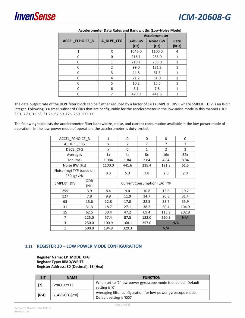
Accelerometer Data Rates and Bandwidths (Low-Noise Mode)
ACCEL_FCHOICE_B A_DLPF_CFG
Accelerometer
3-dB BW (Hz)
Noise BW (Hz)
Rate (kHz)
1 X 1046.0 1100.0 4
0 0 218.1 235.0 1
0 1 218.1 235.0 1
0 2 99.0 121.3 1
0 3 44.8 61.5 1
0 4 21.2 31.0 1
0 5 10.2 15.5 1
0 6 5.1 7.8 1
0 7 420.0 441.6 1
The data output rate of the DLPF filter block can be further reduced by a factor of 1/(1+SMPLRT_DIV), where SMPLRT_DIV is an 8-bit integer. Following is a small subset of ODRs that are configurable for the accelerometer in the low-noise mode in this manner (Hz): 3.91, 7.81, 15.63, 31.25, 62.50, 125, 250, 500, 1K. The following table lists the accelerometer filter bandwidths, noise, and current consumption available in the low-power mode of operation. In the low-power mode of operation, the accelerometer is duty-cycled.
ACCEL_FCHOICE_B 1 0 0 0 0
A_DLPF_CFG x 7 7 7 7
DEC2_CFG x 0 1 2 3
Averages 1x 4x 8x 16x 32x
Ton (ms) 1.084 1.84 2.84 4.84 8.84
Noise BW (Hz) 1100.0 441.6 235.4 121.3 61.5
Noise (mg) TYP based on
250µg/Hz 8.3 5.3 3.8 2.8 2.0
SMPLRT_DIV ODR (Hz)
Current Consumption (µA) TYP
255 3.9 8.4 9.4 10.8 13.6 19.2
127 7.8 9.8 11.9 14.7 20.3 31.4
63 15.6 12.8 17.0 22.5 33.7 55.9
31 31.3 18.7 27.1 38.2 60.4 104.9
15 62.5 30.4 47.2 69.4 113.9 202.8
7 125.0 57.4 87.5 132.0 220.9 N/A
3 250.0 100.9 168.1 257.0 N/A
1 500.0 194.9 329.3 N/A
3.11 REGISTER 30 – LOW POWER MODE CONFIGURATION
Register Name: LP_MODE_CFG Register Type: READ/WRITE Register Address: 30 (Decimal); 1E (Hex)
BIT NAME FUNCTION
[7] GYRO_CYCLE When set to ‘1’ low-power gyroscope mode is enabled. Default setting is ‘0’
[6:4] G_AVGCFG[2:0] Averaging filter configuration for low-power gyroscope mode. Default setting is ‘000’

ICM-20608-G
Page 12 of 23 Document Number: RM-000030 Revision: 1.0
[3:0] LPOSC_CLKSEL
Sets the frequency of waking up the chip to take a sample of accel data – the low power accel Output Data Rate
LPOSC_CLKSEL Output Frequency (Hz)
0 0.24
1 0.49
2 0.98
3 1.95
4 3.91
5 7.81
6 15.63
7 31.25
8 62.50
9 125
10 250
11 500
12-15 Reserved
ICM-20608-G
Page 13 of 23 Document Number: RM-000030 Revision: 1.0
To operate in gyroscope low-power mode or 6-axis low-power mode, GYRO_CYCLE should be set to ‘1.’ Gyroscope filter configuration is determined by G_AVGCFG[2:0] that sets the averaging filter configuration. It is not dependent on DLPF_CFG[2:0]. The following table shows some example configurations for gyroscope low power mode.
FCHOICE_B 0 0 0 0 0 0 0 0
G_AVGCFG 0 1 2 3 4 5 6 7
Averages 1x 2x 4x 8x 16x 32x 64x 128x
Ton (ms) 1.73 2.23 3.23 5.23 9.23 17.23 33.23 65.23
Noise BW (Hz) 650.8 407.1 224.2 117.4 60.2 30.6 15.6 8.0
Noise (dps) TYP based on
0.008º/s/Hz 0.20 0.16 0.12 0.09 0.06 0.04 0.03 0.02
SMPLRT_DIV ODR (Hz)
Current Consumption (mA) TYP
255 3.9 1.3 1.3 1.3 1.3 1.4 1.4 1.5 1.8
99 10.0 1.3 1.3 1.4 1.4 1.5 1.6 1.9 2.5
64 15.4 1.4 1.4 1.4 1.5 1.6 1.8 2.2 N/A
32 30.3 1.4 1.4 1.5 1.6 1.8 2.2 N/A
19 50.0 1.5 1.5 1.6 1.8 2.1 2.8
9 100.0 1.6 1.7 1.9 2.2 3.0 N/A
7 125.0 1.7 1.8 2.0 2.5 N/A
4 200.0 1.9 2.1 2.5 N/A
3 250.0 2.1 2.3 2.7
2 333.3 2.3 2.6 N/A
1 500.0 2.9 N/A
3.12 REGISTER 31 – WAKE-ON MOTION THRESHOLD (ACCELEROMETER)
Register Name: ACCEL_WOM_THR Register Type: READ/WRITE Register Address: 31 (Decimal); 1F (Hex)
BIT NAME FUNCTION
[7:0] WOM_THR[7:0] This register holds the threshold value for the Wake on Motion Interrupt for accelerometer.

ICM-20608-G
Page 14 of 23 Document Number: RM-000030 Revision: 1.0
3.13 REGISTER 35 – FIFO ENABLE
Register Name: FIFO_EN Register Type: READ/WRITE Register Address: 35 (Decimal); 23 (Hex)
BIT NAME FUNCTION
[7] TEMP_FIFO_EN 1 – Write TEMP_OUT_H and TEMP_OUT_L to the FIFO at the sample rate; If enabled, buffering of data occurs even if data path is in standby. 0 – function is disabled
[6] XG_FIFO_EN 1 – Write GYRO_XOUT_H and GYRO_XOUT_L to the FIFO at the sample rate; If enabled, buffering of data occurs even if data path is in standby. 0 – function is disabled
[5] YG_FIFO_EN
1 – Write GYRO_YOUT_H and GYRO_YOUT_L to the FIFO at the sample rate; If enabled, buffering of data occurs even if data path is in standby. 0 – function is disabled NOTE: Enabling any one of the bits corresponding to the Gyros or Temp data paths, data is buffered into the FIFO even though that data path is not enabled.
[4] ZG_FIFO_EN 1 – Write GYRO_ZOUT_H and GYRO_ZOUT_L to the FIFO at the sample rate; If enabled, buffering of data occurs even if data path is in standby. 0 – function is disabled
[3] ACCEL_FIFO_EN 1 – write ACCEL_XOUT_H, ACCEL_XOUT_L, ACCEL_YOUT_H, ACCEL_YOUT_L, ACCEL_ZOUT_H, and ACCEL_ZOUT_L to the FIFO at the sample rate; 0 – function is disabled
[2:0] - Reserved
3.14 REGISTER 54 – FSYNC INTERRUPT STATUS Register Name: FSYNC_INT Register Type: READ to CLEAR Register Address: 54 (Decimal); 36 (Hex)
BIT NAME FUNCTION
[7] FSYNC_INT This bit automatically sets to 1 when a FSYNC interrupt has been generated. The bit clears to 0 after the register has been read.
3.15 REGISTER 55 – INT/DRDY PIN / BYPASS ENABLE CONFIGURATION
Register Name: INT_PIN_CFG Register Type: READ/WRITE Register Address: 55 (Decimal); 37 (Hex)
BIT NAME FUNCTION
[7] INT_LEVEL 1 – The logic level for INT/DRDY pin is active low. 0 – The logic level for INT/DRDY pin is active high.
[6] INT_OPEN 1 – INT/DRDY pin is configured as open drain. 0 – INT/DRDY pin is configured as push-pull.
[5] LATCH_INT_EN 1 – INT/DRDY pin level held until interrupt status is cleared. 0 – INT/DRDY pin indicates interrupt pulse’s width is 50us.
[4] INT_RD_CLEAR 1 – Interrupt status is cleared if any read operation is performed. 0 – Interrupt status is cleared only by reading INT_STATUS register
[3] FSYNC_INT_LEVEL 1 – The logic level for the FSYNC pin as an interrupt is active low. 0 – The logic level for the FSYNC pin as an interrupt is active high.

ICM-20608-G
Page 15 of 23 Document Number: RM-000030 Revision: 1.0
BIT NAME FUNCTION
[2] FSYNC_INT_MODE_EN When this bit is equal to 1, the FSYNC pin will trigger an interrupt when it transitions to the level specified by FSYNC_INT_LEVEL. When this bit is equal to 0, the FSYNC pin is disabled from causing an interrupt.
[1] - Reserved
[0] - Always set to 0
3.16 REGISTER 56 – INTERRUPT ENABLE
Register Name: INT_ENABLE Register Type: READ/WRITE Register Address: 56 (Decimal); 38 (Hex)
BIT NAME FUNCTION
[7:5] WOM_INT_EN[7:5] 111 – Enable WoM interrupt on accelerometer. 000 – Disable WoM interrupt on accelerometer.
[4] FIFO_OFLOW_EN 1 – Enables a FIFO buffer overflow to generate an interrupt. 0 – Function is disabled.
[3] - Reserved [2] GDRIVE_INT_EN Gyroscope Drive System Ready interrupt enable
[1] - Reserved
[0] DATA_RDY_INT_EN Data ready interrupt enable
3.17 REGISTER 58 – INTERRUPT STATUS
Register Name: INT_STATUS Register Type: READ to CLEAR Register Address: 58 (Decimal); 3A (Hex)
BIT NAME FUNCTION
[7:5] WOM_INT
Accelerometer WoM interrupt status. Cleared on Read. 111 – WoM interrupt on accelerometer
[4] FIFO_OFLOW_INT This bit automatically sets to 1 when a FIFO buffer overflow has been generated. The bit clears to 0 after the register has been read.
[3] - Reserved.
[2] GDRIVE_INT Gyroscope Drive System Ready interrupt
[1] - Reserved.
[0] DATA_RDY_INT This bit automatically sets to 1 when a Data Ready interrupt is generated. The bit clears to 0 after the register has been read.

ICM-20608-G
Page 16 of 23 Document Number: RM-000030 Revision: 1.0
3.18 REGISTERS 59 TO 64 – ACCELEROMETER MEASUREMENTS
Register Name: ACCEL_XOUT_H Register Type: READ only Register Address: 59 (Decimal); 3B (Hex)
BIT NAME FUNCTION
[7:0] ACCEL_XOUT_H[15:8] High byte of accelerometer x-axis data.
Register Name: ACCEL_XOUT_L Register Type: READ only Register Address: 60 (Decimal); 3C (Hex)
BIT NAME FUNCTION
[7:0] ACCEL_XOUT_L[7:0] Low byte of accelerometer x-axis data.
Register Name: ACCEL_YOUT_H Register Type: READ only Register Address: 61 (Decimal); 3D (Hex)
BIT NAME FUNCTION
[7:0] ACCEL_YOUT_H[15:8] High byte of accelerometer y-axis data.
Register Name: ACCEL_YOUT_L Register Type: READ only Register Address: 62 (Decimal); 3E (Hex)
BIT NAME FUNCTION
[7:0] ACCEL_YOUT_L[7:0] Low byte of accelerometer y-axis data.
Register Name: ACCEL_ZOUT_H Register Type: READ only Register Address: 63 (Decimal); 3F (Hex)
BIT NAME FUNCTION
[7:0] ACCEL_ZOUT_H[15:8] High byte of accelerometer z-axis data.
Register Name: ACCEL_ZOUT_L Register Type: READ only Register Address: 64 (Decimal); 40 (Hex)
BIT NAME FUNCTION
[7:0] ACCEL_ZOUT_L[7:0] Low byte of accelerometer z-axis data.
3.19 REGISTERS 65 AND 66 – TEMPERATURE MEASUREMENT
Register Name: TEMP_OUT_H Register Type: READ only Register Address: 65 (Decimal); 41 (Hex)
BIT NAME FUNCTION
[7:0] TEMP_OUT[15:8] High byte of the temperature sensor output
Register Name: TEMP_OUT_L Register Type: READ only Register Address: 66 (Decimal); 42 (Hex)
BIT NAME FUNCTION
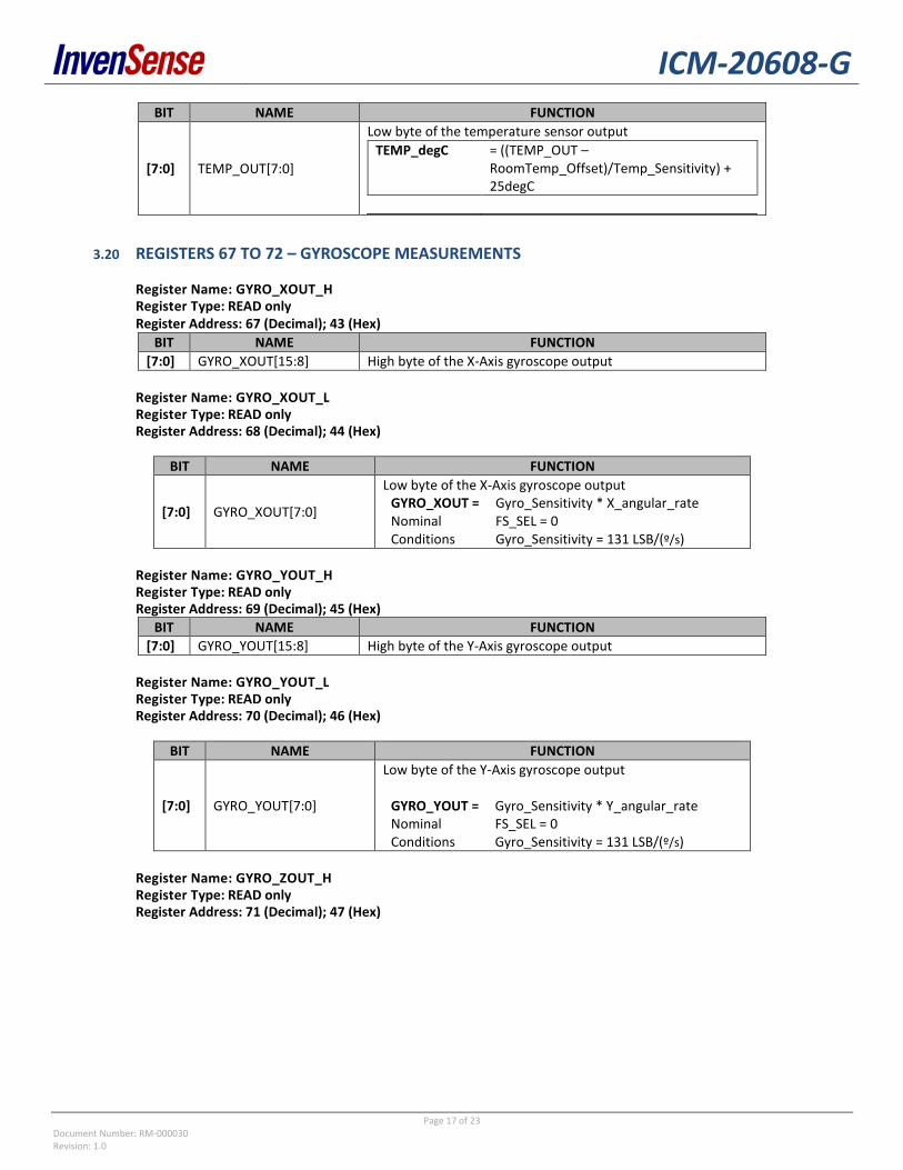
ICM-20608-G
Page 17 of 23 Document Number: RM-000030 Revision: 1.0
BIT NAME FUNCTION
[7:0] TEMP_OUT[7:0]
Low byte of the temperature sensor output TEMP_degC = ((TEMP_OUT –
RoomTemp_Offset)/Temp_Sensitivity) + 25degC
3.20 REGISTERS 67 TO 72 – GYROSCOPE MEASUREMENTS Register Name: GYRO_XOUT_H Register Type: READ only Register Address: 67 (Decimal); 43 (Hex)
BIT NAME FUNCTION
[7:0] GYRO_XOUT[15:8] High byte of the X-Axis gyroscope output
Register Name: GYRO_XOUT_L Register Type: READ only Register Address: 68 (Decimal); 44 (Hex)
BIT NAME FUNCTION
[7:0] GYRO_XOUT[7:0]
Low byte of the X-Axis gyroscope output GYRO_XOUT = Gyro_Sensitivity * X_angular_rate Nominal Conditions
FS_SEL = 0 Gyro_Sensitivity = 131 LSB/(º/s)
Register Name: GYRO_YOUT_H Register Type: READ only Register Address: 69 (Decimal); 45 (Hex)
BIT NAME FUNCTION
[7:0] GYRO_YOUT[15:8] High byte of the Y-Axis gyroscope output
Register Name: GYRO_YOUT_L Register Type: READ only Register Address: 70 (Decimal); 46 (Hex)
BIT NAME FUNCTION
[7:0] GYRO_YOUT[7:0]
Low byte of the Y-Axis gyroscope output
GYRO_YOUT = Gyro_Sensitivity * Y_angular_rate Nominal Conditions
FS_SEL = 0 Gyro_Sensitivity = 131 LSB/(º/s)
Register Name: GYRO_ZOUT_H Register Type: READ only Register Address: 71 (Decimal); 47 (Hex)

ICM-20608-G
Page 18 of 23 Document Number: RM-000030 Revision: 1.0
BIT NAME FUNCTION
[7:0] GYRO_ZOUT[15:8] High byte of the Z-Axis gyroscope output
Register Name: GYRO_ZOUT_L Register Type: READ only Register Address: 72 (Decimal); 48 (Hex)
3.21 REGISTER 104 – SIGNAL PATH RESET Register Name: SIGNAL_PATH_RESET Register Type: READ/WRITE Register Address: 104 (Decimal); 68 (Hex)
BIT NAME FUNCTION
[7:2] - Reserved
[1] ACCEL_RST Reset accel digital signal path. Note: Sensor registers are not cleared. Use SIG_COND_RST to clear sensor registers.
[0] TEMP_RST Reset temp digital signal path. Note: Sensor registers are not cleared. Use SIG_COND_RST to clear sensor registers.
3.22 REGISTER 105 – ACCELEROMETER INTELLIGENCE CONTROL
Register Name: ACCEL_INTEL_CTRL Register Type: READ/WRITE Register Address: 105 (Decimal); 69 (Hex)
BIT NAME FUNCTION
[7] ACCEL_INTEL_EN This bit enables the Wake-on-Motion detection logic
[6] ACCEL_INTEL_MODE 0 – Do not use 1 – Compare the current sample with the previous sample
[5:0] - Reserved
BIT NAME FUNCTION
[7:0] GYRO_YOUT[7:0]
Low byte of the Z-Axis gyroscope output GYRO_ZOUT =
Gyro_Sensitivity * Z_angular_rate
Nominal Conditions
FS_SEL = 0 Gyro_Sensitivity = 131 LSB/(º/s)
ICM-20608-G
Page 19 of 23 Document Number: RM-000030 Revision: 1.0
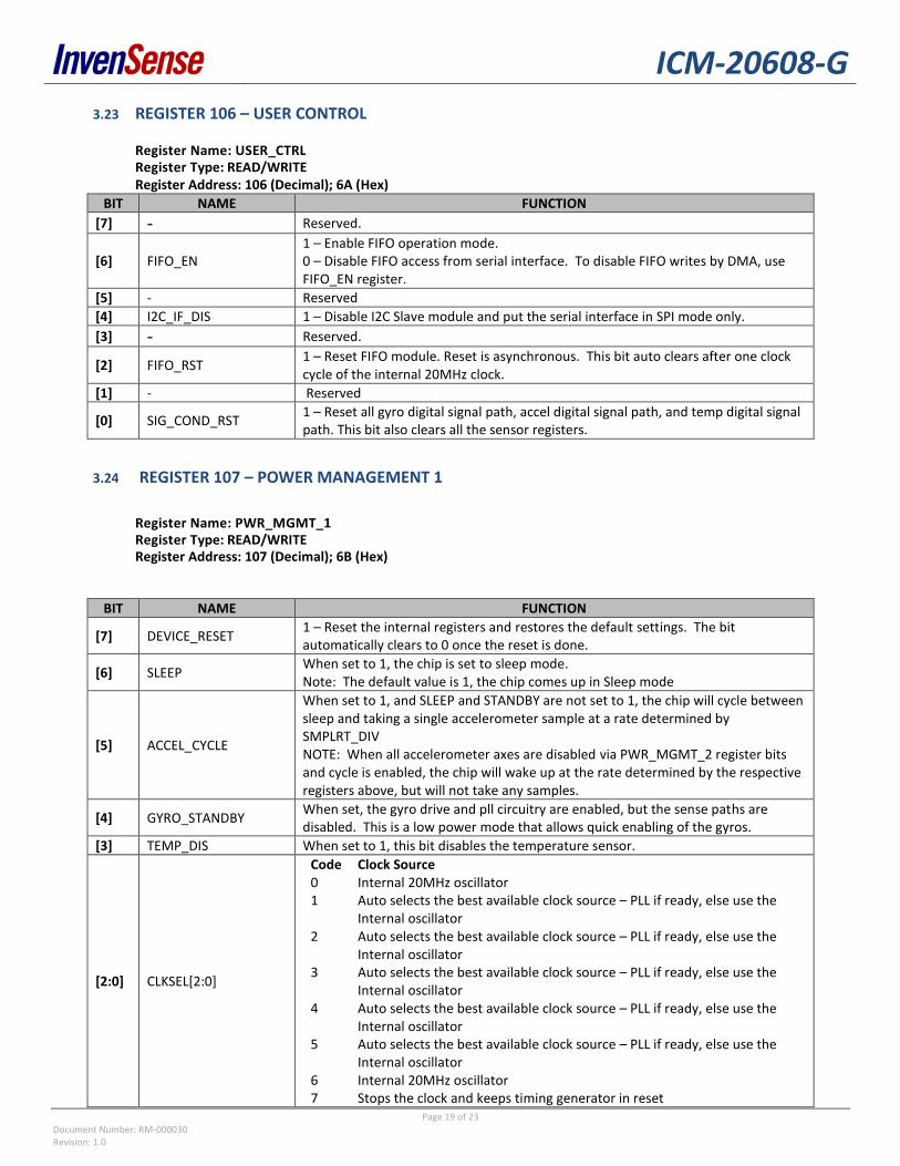
3.23 REGISTER 106 – USER CONTROL
Register Name: USER_CTRL Register Type: READ/WRITE Register Address: 106 (Decimal); 6A (Hex)
BIT NAME FUNCTION
[7] - Reserved.
[6] FIFO_EN 1 – Enable FIFO operation mode. 0 – Disable FIFO access from serial interface. To disable FIFO writes by DMA, use FIFO_EN register.
[5] - Reserved [4] I2C_IF_DIS 1 – Disable I2C Slave module and put the serial interface in SPI mode only. [3] - Reserved.
[2] FIFO_RST 1 – Reset FIFO module. Reset is asynchronous. This bit auto clears after one clock cycle of the internal 20MHz clock.
[1] - Reserved
[0] SIG_COND_RST 1 – Reset all gyro digital signal path, accel digital signal path, and temp digital signal path. This bit also clears all the sensor registers.
3.24 REGISTER 107 – POWER MANAGEMENT 1
Register Name: PWR_MGMT_1 Register Type: READ/WRITE Register Address: 107 (Decimal); 6B (Hex)
BIT NAME FUNCTION
[7] DEVICE_RESET 1 – Reset the internal registers and restores the default settings. The bit automatically clears to 0 once the reset is done.
[6] SLEEP When set to 1, the chip is set to sleep mode. Note: The default value is 1, the chip comes up in Sleep mode
[5] ACCEL_CYCLE
When set to 1, and SLEEP and STANDBY are not set to 1, the chip will cycle between sleep and taking a single accelerometer sample at a rate determined by SMPLRT_DIV NOTE: When all accelerometer axes are disabled via PWR_MGMT_2 register bits and cycle is enabled, the chip will wake up at the rate determined by the respective registers above, but will not take any samples.
[4] GYRO_STANDBY When set, the gyro drive and pll circuitry are enabled, but the sense paths are disabled. This is a low power mode that allows quick enabling of the gyros.
[3] TEMP_DIS When set to 1, this bit disables the temperature sensor.
[2:0] CLKSEL[2:0]
Code Clock Source 0 Internal 20MHz oscillator 1 Auto selects the best available clock source – PLL if ready, else use the
Internal oscillator 2 Auto selects the best available clock source – PLL if ready, else use the
Internal oscillator 3 Auto selects the best available clock source – PLL if ready, else use the
Internal oscillator 4 Auto selects the best available clock source – PLL if ready, else use the
Internal oscillator 5 Auto selects the best available clock source – PLL if ready, else use the
Internal oscillator 6 Internal 20MHz oscillator 7 Stops the clock and keeps timing generator in reset

ICM-20608-G
Page 20 of 23 Document Number: RM-000030 Revision: 1.0
Note: The default value of CLKSEL[2:0] is 000. It is required that CLKSEL[2:0] be set to 001 to achieve full gyroscope performance.
3.25 REGISTER 108 – POWER MANAGEMENT 2
Register Name: PWR_MGMT_2 Register Type: READ/WRITE Register Address: 108 (Decimal); 6C (Hex)
BIT NAME FUNCTION
[7] FIFO_LP_EN 1 – Enable FIFO in low-power accelerometer mode. Default setting is 0. [6] - Reserved.
[5] STBY_XA 1 – X accelerometer is disabled 0 – X accelerometer is on
[4] STBY_YA 1 – Y accelerometer is disabled 0 – Y accelerometer is on
[3] STBY_ZA 1 – Z accelerometer is disabled 0 – Z accelerometer is on
[2] STBY_XG 1 – X gyro is disabled 0 – X gyro is on
[1] STBY_YG 1 – Y gyro is disabled 0 – Y gyro is on
[0] STBY_ZG 1 – Z gyro is disabled 0 – Z gyro is on
3.26 REGISTER 114 AND 115 – FIFO COUNT REGISTERS
Register Name: FIFO_COUNTH Register Type: READ Only Register Address: 114 (Decimal); 72 (Hex)
BIT NAME FUNCTION
[7:5] - Reserved
[4:0] FIFO_COUNT[12:8] High Bits, count indicates the number of written bytes in the FIFO. Reading this byte latches the data for both FIFO_COUNTH, and FIFO_COUNTL.
Register Name: FIFO_COUNTL Register Type: READ Only Register Address: 115 (Decimal); 73 (Hex)

ICM-20608-G
Page 21 of 23 Document Number: RM-000030 Revision: 1.0
BIT NAME FUNCTION
[7:0] FIFO_COUNT[7:0] Low Bits, count indicates the number of written bytes in the FIFO. NOTE: Must read FIFO_COUNTH to latch new data for both FIFO_COUNTH and FIFO_COUNTL.
3.27 REGISTER 116 – FIFO READ WRITE
Register Name: FIFO_R_W Register Type: READ/WRITE Register Address: 116 (Decimal); 74 (Hex)
BIT NAME FUNCTION
[7:0] FIFO_DATA[7:0] Read/Write command provides Read or Write operation for the FIFO.
Description: This register is used to read and write data from the FIFO buffer. Data is written to the FIFO in order of register number (from lowest to highest). If all the FIFO enable flags (see below) are enabled, the contents of registers 59 through 72 will be written in order at the Sample Rate. The contents of the sensor data registers (Registers 59 to 72) are written into the FIFO buffer when their corresponding FIFO enable flags are set to 1 in FIFO_EN (Register 35). If the FIFO buffer has overflowed, the status bit FIFO_OFLOW_INT is automatically set to 1. This bit is located in INT_STATUS (Register 58). When the FIFO buffer has overflowed, the oldest data will be lost and new data will be written to the FIFO unless register 26 CONFIG, bit[6] FIFO_MODE = 1. If the FIFO buffer is empty, reading register FIFO_DATA will return a unique value of 0xFF until new data is available. Normal data is precluded from ever indicating 0xFF, so 0xFF gives a trustworthy indication of FIFO empty.
3.28 REGISTER 117 – WHO AM I
Register Name: WHO_AM_I Register Type: READ only Register Address: 117 (Decimal); 75 (Hex)
BIT NAME FUNCTION
[7:0] WHOAMI Register to indicate to user which device is being accessed.
This register is used to verify the identity of the device. The contents of WHOAMI is an 8-bit device ID. The default value of the register is 0xAF. This is different from the I2C address of the device as seen on the slave I2C controller by the applications processor. The I2C address of the ICM-20608-G is 0x68 or 0x69 depending upon the value driven on AD0 pin.
3.29 REGISTERS 119, 120, 122, 123, 125, 126 ACCELEROMETER OFFSET REGISTERS
Register Name: XA_OFFSET_H Register Type: READ/WRITE Register Address: 119 (Decimal); 77 (Hex)
BIT NAME FUNCTION
[7:0] XA_OFFS[14:7] Upper bits of the X accelerometer offset cancellation. +/- 16g Offset cancellation in all Full Scale modes, 15 bit 0.98-mg steps

ICM-20608-G
Page 22 of 23 Document Number: RM-000030 Revision: 1.0
Register Name: XA_OFFSET_L Register Type: READ/WRITE
Register Address: 120 (Decimal); 78 (Hex)
BIT NAME FUNCTION
[7:1] XA_OFFS[6:0] Lower bits of the X accelerometer offset cancellation. +/- 16g Offset cancellation in all Full Scale modes, 15 bit 0.98-mg steps
[0] - Reserved
Register Name: YA_OFFSET_H Register Type: READ/WRITE Register Address: 122 (Decimal); 7A (Hex)
BIT NAME FUNCTION
[7:0] YA_OFFS[14:7] Upper bits of the Y accelerometer offset cancellation. +/- 16g Offset cancellation in all Full Scale modes, 15 bit 0.98-mg steps
Register Name: YA_OFFSET_L Register Type: READ/WRITE Register Address: 123 (Decimal); 7B (Hex)
BIT NAME FUNCTION
[7:1] YA_OFFS[6:0] Lower bits of the Y accelerometer offset cancellation. +/- 16g Offset cancellation in all Full Scale modes, 15 bit 0.98-mg steps
[0] - Reserved
Register Name: ZA_OFFSET_H Register Type: READ/WRITE Register Address: 125 (Decimal); 7D (Hex)
BIT NAME FUNCTION
[7:0] ZA_OFFS[14:7] Upper bits of the Z accelerometer offset cancellation. +/- 16g Offset cancellation in all Full Scale modes, 15 bit 0.98-mg steps
Register Name: ZA_OFFSET_L Register Type: READ/WRITE Register Address: 126 (Decimal); 7E (Hex)
BIT NAME FUNCTION
[7:1] ZA_OFFS[6:0] Lower bits of the Z accelerometer offset cancellation. +/- 16g Offset cancellation in all Full Scale modes, 15 bit 0.98-mg steps
[0] - Reserved

ICM-20608-G
Page 23 of 23 Document Number: RM-000030 Revision: 1.0
4 REVISION HISTORY
Revision Date Revision Description
06/15/2015 1.0 Initial Release
This information furnished by InvenSense is believed to be accurate and reliable. However, no responsibility is assumed by InvenSense for its use, or for any infringements of patents or other rights of third parties that may result from its use. Specifications are subject to change without notice. InvenSense reserves the right to make changes to this product, including its circuits and software, in order to improve its design and/or performance, without prior notice. InvenSense makes no warranties, neither expressed nor implied, regarding the information and specifications contained in this document. InvenSense assumes no responsibility for any claims or damages arising from information contained in this document, or from the use of products and services detailed therein. This includes, but is not limited to, claims or damages based on the infringement of patents, copyrights, mask work and/or other intellectual property rights. Certain intellectual property owned by InvenSense and described in this document is patent protected. No license is granted by implication or otherwise under any patent or patent rights of InvenSense. This publication supersedes and replaces all information previously supplied. Trademarks that are registered trademarks are the property of their respective companies. InvenSense sensors should not be used or sold in the development, storage, production or utilization of any conventional or mass-destructive weapons or for any other weapons or life threatening applications, as well as in any other life critical applications such as medical equipment, transportation, aerospace and nuclear instruments, undersea equipment, power plant equipment, disaster prevention and crime prevention equipment.
©2015 InvenSense, Inc. All rights reserved. InvenSense, MotionTracking, MotionProcessing, MotionProcessor, MotionFusion, MotionApps, DMP, and the InvenSense logo are trademarks of InvenSense, Inc. Other company and product names may be trademarks of the respective companies with which they are associated.
.
©2015 InvenSense, Inc. All rights reserved.