Hot Chips 2017 · Hot Chips 2017 Xilinx 16nm Datacenter Device Family with ... HBM-IO HBM-PHY MC1...
22
Hot Chips 2017 Xilinx 16nm Datacenter Device Family with In-Package HBM and CCIX Interconnect Gaurav Singh Sagheer Ahmad, Ralph Wittig, Millind Mittal, Ygal Arbel, Arun VR, Suresh Ramalingam, Kiran Puranik, Gamal Refai-Ahmed, Rafe Camarota, Mike Wissolik
Transcript of Hot Chips 2017 · Hot Chips 2017 Xilinx 16nm Datacenter Device Family with ... HBM-IO HBM-PHY MC1...

Hot Chips 2017Xilinx 16nm Datacenter Device Family withIn-Package HBM and CCIX InterconnectGaurav SinghSagheer Ahmad, Ralph Wittig, Millind Mittal, Ygal Arbel, Arun VR, Suresh Ramalingam, Kiran Puranik, Gamal Refai-Ahmed, Rafe Camarota, Mike Wissolik
© Copyright 2017 Xilinx.
Page 2
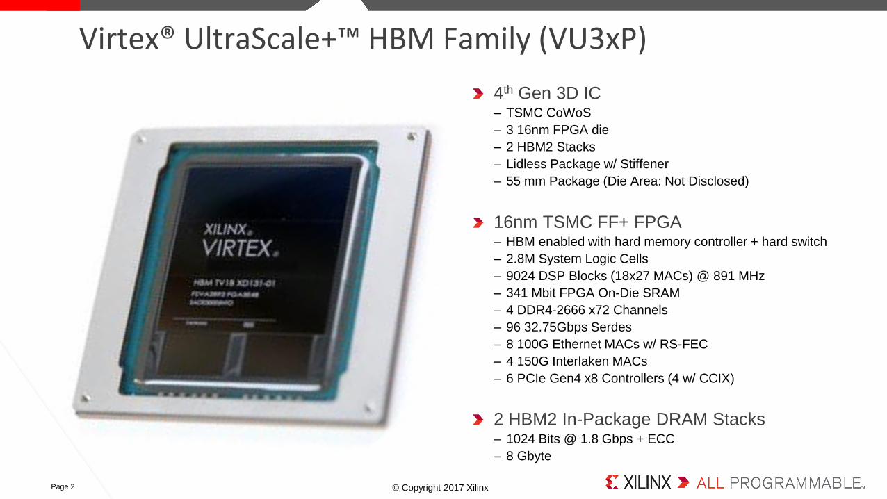
4th Gen 3D IC– TSMC CoWoS
– 3 16nm FPGA die
– 2 HBM2 Stacks
– Lidless Package w/ Stiffener
– 55 mm Package (Die Area: Not Disclosed)
16nm TSMC FF+ FPGA– HBM enabled with hard memory controller + hard switch
– 2.8M System Logic Cells
– 9024 DSP Blocks (18x27 MACs) @ 891 MHz
– 341 Mbit FPGA On-Die SRAM
– 4 DDR4-2666 x72 Channels
– 96 32.75Gbps Serdes
– 8 100G Ethernet MACs w/ RS-FEC
– 4 150G Interlaken MACs
– 6 PCIe Gen4 x8 Controllers (4 w/ CCIX)
2 HBM2 In-Package DRAM Stacks– 1024 Bits @ 1.8 Gbps + ECC
– 8 Gbyte
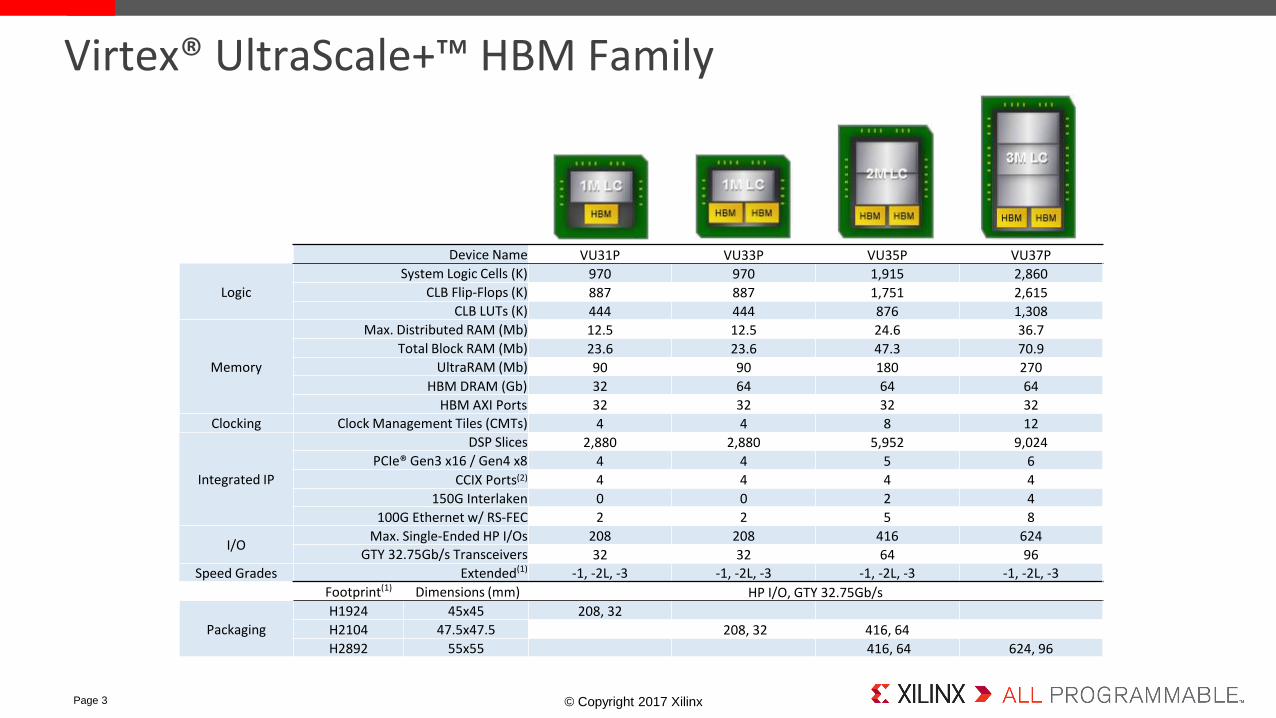
Virtex® UltraScale+™ HBM Family (VU3xP)
© Copyright 2017 Xilinx.
Page 3
Virtex® UltraScale+™ HBM Family
Device Name VU31P VU33P VU35P VU37P
Logic
System Logic Cells (K) 970 970 1,915 2,860
CLB Flip-Flops (K) 887 887 1,751 2,615
CLB LUTs (K) 444 444 876 1,308
Memory
Max. Distributed RAM (Mb) 12.5 12.5 24.6 36.7
Total Block RAM (Mb) 23.6 23.6 47.3 70.9
UltraRAM (Mb) 90 90 180 270
HBM DRAM (Gb) 32 64 64 64
HBM AXI Ports 32 32 32 32
Clocking Clock Management Tiles (CMTs) 4 4 8 12
Integrated IP
DSP Slices 2,880 2,880 5,952 9,024
PCIe® Gen3 x16 / Gen4 x8 4 4 5 6
CCIX Ports(2) 4 4 4 4
150G Interlaken 0 0 2 4
100G Ethernet w/ RS-FEC 2 2 5 8
I/OMax. Single-Ended HP I/Os 208 208 416 624
GTY 32.75Gb/s Transceivers 32 32 64 96
Speed Grades Extended(1) -1, -2L, -3 -1, -2L, -3 -1, -2L, -3 -1, -2L, -3
Footprint(1) Dimensions (mm) HP I/O, GTY 32.75Gb/s
Packaging
H1924 45x45 208, 32
H2104 47.5x47.5 208, 32 416, 64
H2892 55x55 416, 64 624, 96
© Copyright 2017 Xilinx.
Page 4
Agenda o Application Drivers
o HBM: Design Changes
o HBM: Package/Thermal Consideration
o CCIX: What is CCIX
o CCIX: How CCIX is supported

© Copyright 2017 Xilinx.
Datacenter
– Vision Processing (CNN/DNN)
• Higher compute density (2.8MLCs,
9024 DSPs – 32 TOPs INT8)
– Natural Language Processing
(LSTM, RNN)
• Memory bandwidth (weights, fully-
connected layers) 3.6Tbps
– Efficient Host interface
• Multiple PCIe Gen4/CCIX ports
– Seamless heterogenous nodes
• SVM with CCIX
– Memory expansion (CCIX)
Page 5
Application Drivers
400G Networking
– N ports @400G
• x96 high bandwidth interfaces -
32.75Gbps
• x8 100G MACs, 4x Interlaken MACs
• 2.8M LCs for P4 packet processing
• 3.6Tbps HBM2 packet buffering
Data
Analytics
SQL Query
Machine
Learning
Inference
Video
Processing
Transcode
Storage
CompressionNetworking
NFV

© Copyright 2017 Xilinx.
Virtex® UltraScale+™ HBM (VU+HBM): Key Features
Page 6
4GB
Density per HBM
(4H x 8Gb)
230 GB/s
Bandwidth per HBM1024 IO @ 1.8 GTps
Base 16nm FPGA Platform
(GTY, DDR4, URAM, CMAC)
Hard Memory Controller
for HBM
PCIe Hard IP
with CCIX TL
Hard AXI Switch for
Unified and Flexible Addressing

© Copyright 2017 Xilinx.
HBM Integration Benefits
Page 7
VU9P
624 I/O
HBM HBM
VU9P + DDR4 VU37P + HBM2
Bandwidth 85 GB/s 460 GB/s
Power ~27 pJ/bit (memory + IO power) ~7 pJ/bit (memory + 2.5D I/O)
Advantages High density, low cost/bit Highest performance, lowest power/bit
Disadvantages PCB footprint, signal integrity, power Lower DRAM Capacity
DDR4
8x32b (4GB)
VU37P
>3000 2.5D I/O
DDR4
8x32b (4GB)
5X
4X
(Higher bandwidth)
(Higher power efficiency)
Memory B/W
Pe
rfo
rma
nce
GDDR HBM
Additional performance
enabled by HBM
HBM2
2x32Gb (8GB)
© Copyright 2017 Xilinx.
Page 8
HBM Integration
© Copyright 2017 Xilinx.
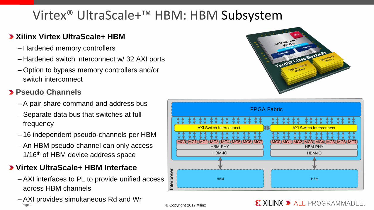
Xilinx Virtex UltraScale+ HBM
– Hardened memory controllers
– Hardened switch interconnect w/ 32 AXI ports
– Option to bypass memory controllers and/or
switch interconnect
Pseudo Channels
– A pair share command and address bus
– Separate data bus that switches at full
frequency
– 16 independent pseudo-channels per HBM
– An HBM pseudo-channel can only access
1/16th of HBM device address space
Virtex UltraScale+ HBM Interface
– AXI interfaces to PL to provide unified access
across HBM channels
– AXI provides simultaneous Rd and WrPage 9
Virtex® UltraScale+™ HBM: HBM Subsystem
FPGA Fabric
MC0
HBM-IO
HBM-PHY
MC1 MC2 MC3 MC4 MC5 MC6 MC7
AXI Switch Interconnect
MC0
HBM-IO
HBM-PHY
MC1 MC2 MC3 MC4 MC5 MC6 MC7
AXI Switch Interconnect
HBM HBM
© Copyright 2017 Xilinx.
Switch Matrix
Page 10
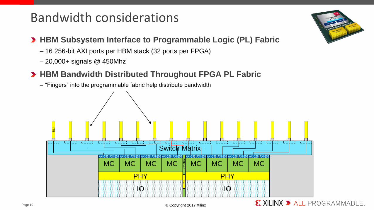
Bandwidth considerations
IO
MC MC MC
PHY
MC
IO
PHY
MC MC MC MC
HBM Subsystem Interface to Programmable Logic (PL) Fabric
– 16 256-bit AXI ports per HBM stack (32 ports per FPGA)
– 20,000+ signals @ 450Mhz
HBM Bandwidth Distributed Throughout FPGA PL Fabric
– “Fingers” into the programmable fabric help distribute bandwidth
BLI
AXI-256 AXI-256 AXI-256 AXI-256 AXI-256 AXI-256 AXI-256 AXI-256 AXI-256 AXI-256 AXI-256 AXI-256 AXI-256 AXI-256 AXI-256 AXI-256
Contr
ol
P
LL
© Copyright 2017 Xilinx.
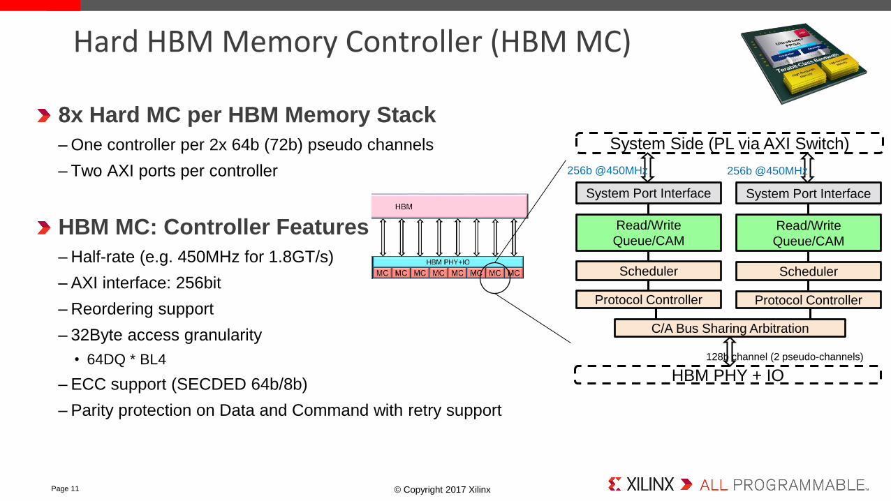
8x Hard MC per HBM Memory Stack
– One controller per 2x 64b (72b) pseudo channels
– Two AXI ports per controller
HBM MC: Controller Features
– Half-rate (e.g. 450MHz for 1.8GT/s)
– AXI interface: 256bit
– Reordering support
– 32Byte access granularity
• 64DQ * BL4
– ECC support (SECDED 64b/8b)
– Parity protection on Data and Command with retry support
Page 11
Hard HBM Memory Controller (HBM MC)
Scheduler
System Port Interface
Read/Write
Queue/CAM
Protocol Controller
256b @450MHz
C/A Bus Sharing Arbitration
System Side (PL via AXI Switch)
HBM PHY + IO
128b channel (2 pseudo-channels)
Scheduler
System Port Interface
Read/Write
Queue/CAM
Protocol Controller
256b @450MHz
© Copyright 2017 Xilinx.
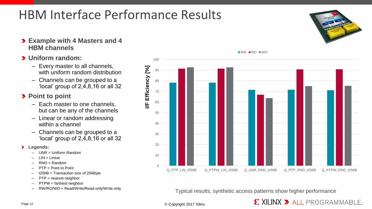
HBM Interface Performance Results
Page 12
Example with 4 Masters and 4 HBM channels
Uniform random:
– Every master to all channels, with uniform random distribution
– Channels can be grouped to a ‘local’ group of 2,4,8,16 or all 32
Point to point
– Each master to one channels, but can be any of the channels
– Linear or random addressing within a channel
– Channels can be grouped to a ‘local’ group of 2,4,8,16 or all 32
Legends:– UNR = Uniform Random
– LIN = Linear
– RND = Random
– PTP = Point to Point
– t256B = Transaction size of 256Byte
– PTP = nearest neighbor
– PTPW = farthest neighbor
– RW/RO/WO = Read/Write/Read-only/Write-only
0
10
20
30
40
50
60
70
80
90
100
Q_PTP_LIN_t256B Q_PTPW_LIN_t256B Q_UNR_RND_t256B Q_PTP_RND_t256B Q_PTPW_RND_t256B
I/F
Eff
icie
nc
y [
%]
RW RO WO
Typical results, synthetic access patterns show higher performance

© Copyright 2017 Xilinx.
Page 13
Packaging
© Copyright 2017 Xilinx.
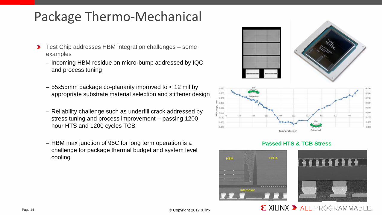
Test Chip addresses HBM integration challenges – some
examples
– Incoming HBM residue on micro-bump addressed by IQC
and process tuning
– 55x55mm package co-planarity improved to < 12 mil by
appropriate substrate material selection and stiffener design
– Reliability challenge such as underfill crack addressed by
stress tuning and process improvement – passing 1200
hour HTS and 1200 cycles TCB
– HBM max junction of 95C for long term operation is a
challenge for package thermal budget and system level
cooling
Page 14
Package Thermo-Mechanical
Passed HTS & TCB Stress
© Copyright 2017 Xilinx.
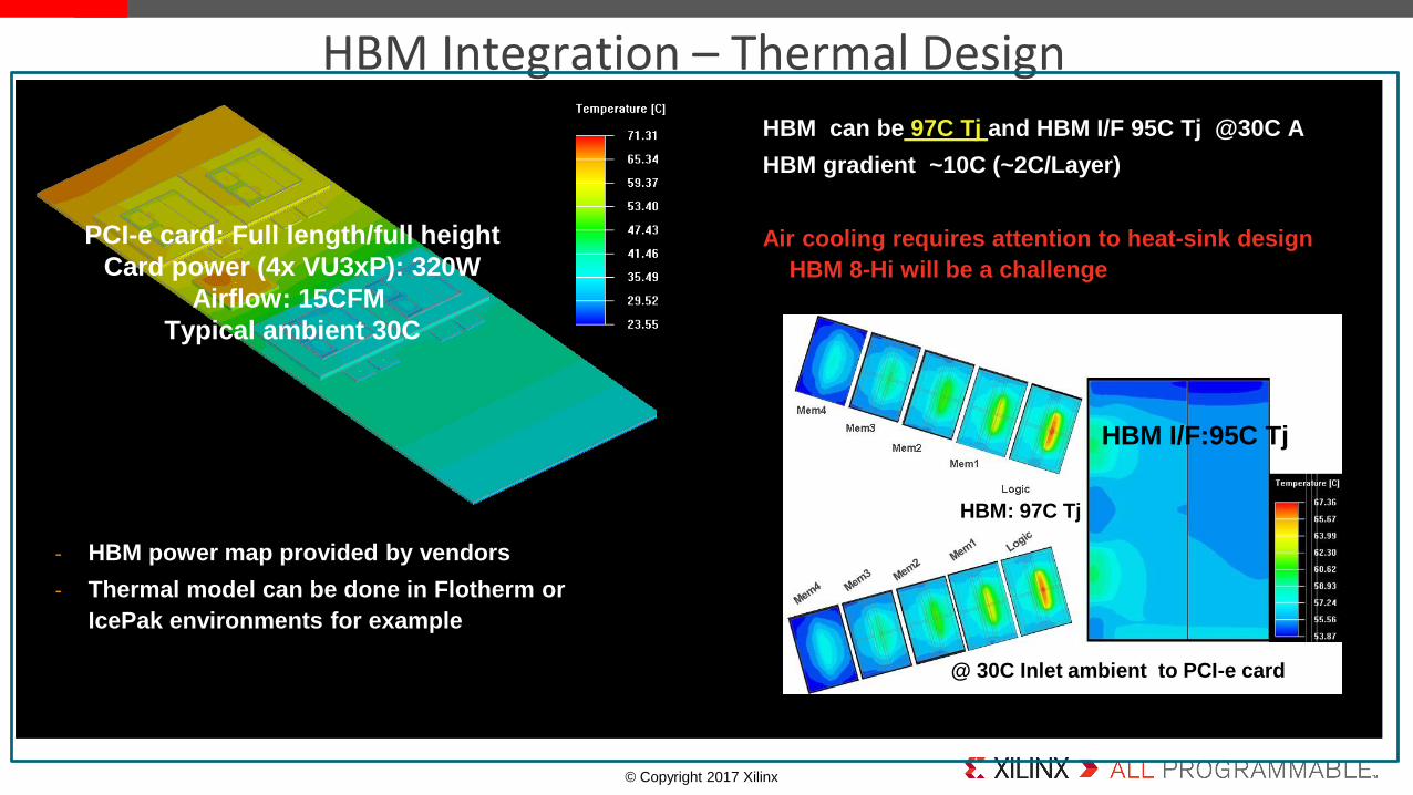
HBM Integration – Thermal Design
HBM can be 97C Tj and HBM I/F 95C Tj @30C A
HBM gradient ~10C (~2C/Layer)
Air cooling requires attention to heat-sink design
HBM 8-Hi will be a challenge
@ 30C Inlet ambient to PCI-e card
HBM I/F:95C Tj
HBM: 97C Tj
PCI-e card: Full length/full height
Card power (4x VU3xP): 320W
Airflow: 15CFM
Typical ambient 30C
- HBM power map provided by vendors
- Thermal model can be done in Flotherm or
IcePak environments for example
© Copyright 2017 Xilinx.
Page 16
CCIX
© Copyright 2017 Xilinx.
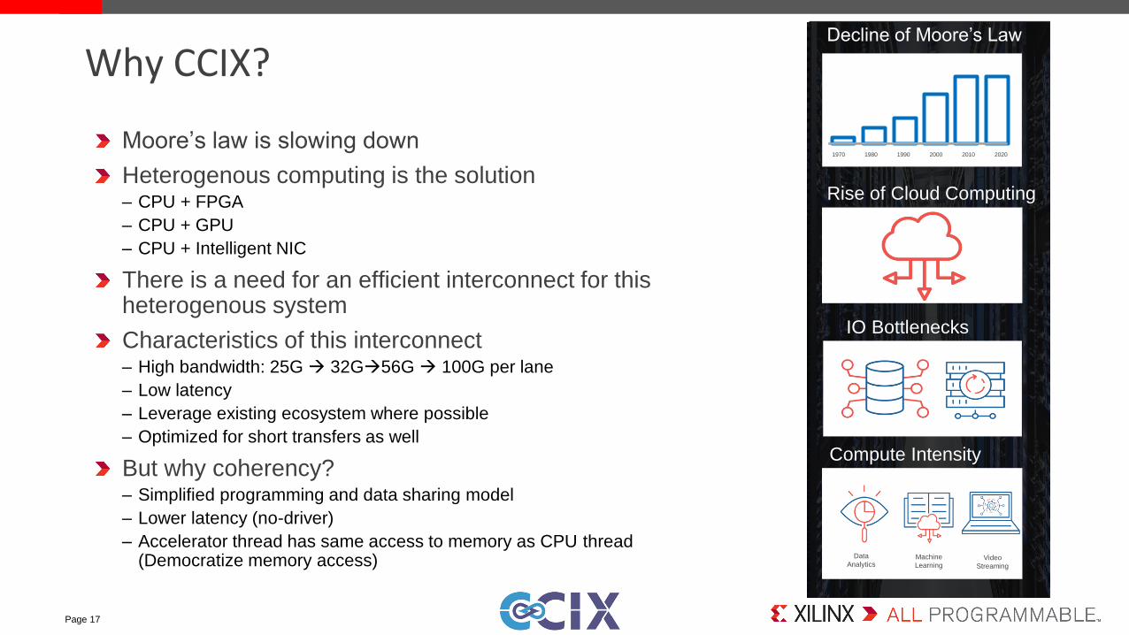
Moore’s law is slowing down
Heterogenous computing is the solution– CPU + FPGA
– CPU + GPU
– CPU + Intelligent NIC
There is a need for an efficient interconnect for this heterogenous system
Characteristics of this interconnect– High bandwidth: 25G 32G56G 100G per lane
– Low latency
– Leverage existing ecosystem where possible
– Optimized for short transfers as well
But why coherency?– Simplified programming and data sharing model
– Lower latency (no-driver)
– Accelerator thread has same access to memory as CPU thread (Democratize memory access)
Page 17
Why CCIX?Decline of Moore’s Law
Rise of Cloud Computing
Compute Intensity
IO Bottlenecks
1970 1980 1990 2000 2010 2020
Data
AnalyticsMachine
LearningVideo
Streaming

© Copyright 2017 Xilinx.
High bandwidth IO– 25Gbps Gen1 (specification complete)
– Backward compatible to 16Gbps and lower speeds
Full capability in the accelerator– Accelerator-processor peer processing (homenode)
– Caching capability
– Memory expansion
Flexible topology– 1 CPU to 1 accelerator
– Option to connect multiple accelerators
Optimized for multi-chip transfers– Low overhead header format
– Message packing and simplified messaging
– Request and Snoop chaining
– Port Aggregation
Full Ecosystem support– Interface IP available from Cadence, Synopsys
– Coherent controllers from ARM, Netspeed, ArterisIP
– Verification IP from Cadence, Synopsys, Avery Design Systems
– How to join: www.ccixconsortium.com (33 members and counting)
Page 18
CCIX SummaryProcessor
Accelerator:
In-line & co-
processor
acceleration
Local
StorageCCIX
Network/
Converged Storage
System
Memory
Proprietary
Coherent
InterfaceSystem
MemoryExtends
system
memory
across
devices
© Copyright 2017 Xilinx.
Page 19
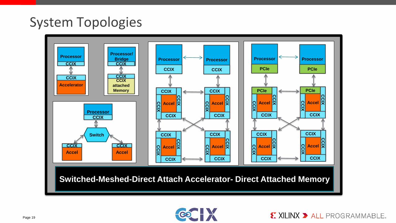
System Topologies
Accel
Processor
CCIX
CCIX
Switch
Accel
CCIX
Accelerator
Processor
CCIX
CCIXCCIX
attached
Memory
Processor/
BridgeCCIX
CCIX
Processor
CCIX
Accel
CCIX
CC
IX
CCIX
CC
IX
Accel
CCIX
CC
IX
CCIX
CC
IX
Accel
CCIX
CC
IX
CCIX
CC
IX
Accel
CCIX
CC
IX
CCIX
CC
IX
Switched-Meshed-Direct Attach Accelerator- Direct Attached Memory
Processor
CCIX
Processor
PCIe
Accel
PCIe
CC
IX
CCIX
CC
IX
Accel
PCIe
CC
IX
CCIX
CC
IX
Accel
CCIX
CC
IX
CCIX
CC
IXAccel
CCIX
CC
IX
CCIX
CC
IX
Processor
PCIe
© Copyright 2017 Xilinx.
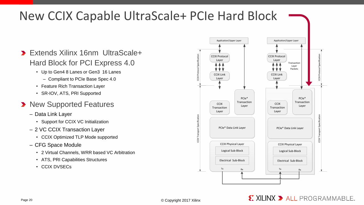
Extends Xilinx 16nm UltraScale+
Hard Block for PCI Express 4.0• Up to Gen4 8 Lanes or Gen3 16 Lanes
– Compliant to PCIe Base Spec 4.0
• Feature Rich Transaction Layer
• SR-IOV, ATS, PRI Supported
New Supported Features
– Data Link Layer
• Support for CCIX VC Initialization
– 2 VC CCIX Transaction Layer
• CCIX Optimized TLP Mode supported
– CFG Space Module
• 2 Virtual Channels, WRR based VC Arbitration
• ATS, PRI Capabilities Structures
• CCIX DVSECs
Page 20
New CCIX Capable UltraScale+ PCIe Hard Block
CCIX Physical Layer
Logical Sub-Block
CCIX Transaction
Layer
PCIe* Data Link Layer
Electrical Sub-Block
Tx Rx
PCIe* Transaction
Layer
CCIX Physical Layer
Logical Sub-Block
CCIX Transaction
Layer
PCIe* Data Link Layer
Electrical Sub-Block
CCIX Link Layer
Tx Rx
PCIe* Transaction
Layer
CCIX Protocol Layer
Application/Upper Layer
CCIX Link Layer
TransactionLayer
Packets
CCIX Protocol Layer
Application/Upper Layer
CC
IX T
ran
spo
rt S
pec
ific
atio
nC
CIX
Pro
toco
l Sp
ecif
icat
ion
CC
IX T
ran
spo
rt S
pec
ific
atio
nC
CIX
Pro
toco
l Sp
ecif
icat
ion
© Copyright 2017 Xilinx.
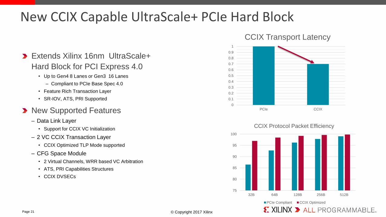
Extends Xilinx 16nm UltraScale+
Hard Block for PCI Express 4.0• Up to Gen4 8 Lanes or Gen3 16 Lanes
– Compliant to PCIe Base Spec 4.0
• Feature Rich Transaction Layer
• SR-IOV, ATS, PRI Supported
New Supported Features
– Data Link Layer
• Support for CCIX VC Initialization
– 2 VC CCIX Transaction Layer
• CCIX Optimized TLP Mode supported
– CFG Space Module
• 2 Virtual Channels, WRR based VC Arbitration
• ATS, PRI Capabilities Structures
• CCIX DVSECs
Page 21
New CCIX Capable UltraScale+ PCIe Hard Block
0
0.1
0.2
0.3
0.4
0.5
0.6
0.7
0.8
0.9
1
PCIe CCIX
CCIX Transport Latency
75
80
85
90
95
100
32B 64B 128B 256B 512B
CCIX Protocol Packet Efficiency
PCIe Compliant CCIX Optimized

© Copyright 2017 Xilinx.
Scalable Family: 4 Devices 1-3 FPGA die, 1-2 HBM2 Stacks
4 Tbps (HBM2 + DDR4-2666): Weight Bandwidth for ML
32 TOPs INT8: Machine Learning Operations
3.6 Tbps HBM2: Packet Buffering for 400G Networking
Coherent Low Latency Host Interface: CCIX
Switchless Peer 2 Peer SVM: CCIX Heterogeneous Scale-Up
96 lanes of PCIe G4: 6 PCIe controllers, 4 CCIX controllers
Page 22
Virtex® UltraScale+™ HBM : Summary