Field Programmable Gate Array (FPGA)
47
Field Programmable Gate Array (FPGA) WaLJŶe Wolf, FPGA Based “LJsteŵ DesigŶ , 2004, Prentice Hall.
Transcript of Field Programmable Gate Array (FPGA)

Field Programmable Gate Array
(FPGA)
Wa e Wolf, FPGA Based “ ste Desig , 2004, Prentice Hall.

INTRODUCTION TO PROGRAMMABLE LOGIC
• Programmable logic requires both hardware and software.
• Programmable logic devices can be programmed to Perform specified logic functions by the manufacturer or by the user.
• One advantage of programmable logic over fixed-function logic is that the devices use much less board space for an equivalent amount of logic.
• Another advantage is that, with programmable logic, designs can be readily changed without rewiring or replacing components.
• Also, a logic design can generally be implemented faster and with less cost with programmable logic than with fixed-function ICs.


Types of Programmable logic Devices
• Many types of programmable logic are available, ranging from small devices that can replace a few fixed-function devices to complex high-density devices that can replace thousands of fixed-function devices.
• Two major categories of user-programmable logic are PLD (programmable logic device) and FPGA (field programmable gate array).
• PLDs are either SPLDs (simple PLDs) or CPLDs (complex PLDs).
Simple Programmable logic Devices
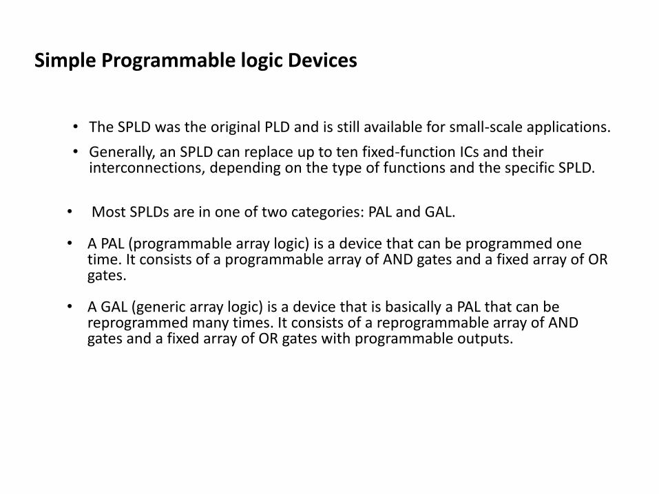
• The SPLD was the original PLD and is still available for small-scale applications.
• Generally, an SPLD can replace up to ten fixed-function ICs and their interconnections, depending on the type of functions and the specific SPLD.
• Most SPLDs are in one of two categories: PAL and GAL. • A PAL (programmable array logic) is a device that can be programmed one
time. It consists of a programmable array of AND gates and a fixed array of OR gates.
• A GAL (generic array logic) is a device that is basically a PAL that can be
reprogrammed many times. It consists of a reprogrammable array of AND gates and a fixed array of OR gates with programmable outputs.

Complex Programmable logic Devices
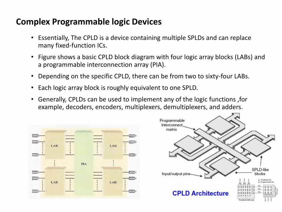
• Essentially, The CPLD is a device containing multiple SPLDs and can replace many fixed-function ICs.
• Figure shows a basic CPLD block diagram with four logic array blocks (LABs) and a programmable interconnection array (PIA).
• Depending on the specific CPLD, there can be from two to sixty-four LABs.
• Each logic array block is roughly equivalent to one SPLD.
• Generally, CPLDs can be used to implement any of the logic functions ,for example, decoders, encoders, multiplexers, demultiplexers, and adders.

Field Programmable Gate Array
• Field programmable gate arrays (FPGAs) are digital integrated circuits (ICs) that
contain configurable (programmable) blocks of logic along with configurable
interconnects between these blocks. Design engineers can configure, or program,
such devices to perform a tremendous variety of tasks.
• The field programmable portion of the FPGA’s name refers to the fact that
its programming takes place in the field (as opposed to devices whose internal
functionality is hardwired by the manufacturer).
• An FPGA is a regular structure of logic cells or modules and interconnect which is
u der the desig er’s co plete co trol. This ea s the user ca desig , progra a d make changes to his circuit whenever he wants.
• An FPGA is generally more complex and has a much higher density than a CPLD.

• The logic blocks in an FPGA are not as complex as the logic array blocks (LABs)
in a CPLD, but generally there are many more of them.

• FPGAs can be used to implement any logical function that an ASIC could
perform. RATHER YOU CAN ALSO BUILD MICROs USING FPGAs. • FPGA are basically made up for the home integration, the user has all the
power of development and changing the logic using very versatile interconnects between logic elements.
• FPGA consist of millions of transistor logic and thousands of logic block
elements, so it is an ultra large scale integration. • Compared to ASIC, FPGAs are home programmable and can be designed using
simple software algorithms.
• The three basic elements in an FPGA are the logic block, the programmable
interconnections, and the input/output (I/O) blocks.
• When the logic blocks are relatively simple, the FPGA architecture is called fine-
grained.
• When the logic blocks are larger and more complex, the architecture is called coarse-grained.
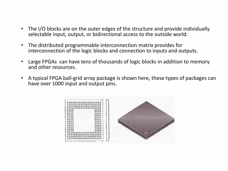
• The I/O blocks are on the outer edges of the structure and provide individually
selectable input, output, or bidirectional access to the outside world.
• The distributed programmable interconnection matrix provides for interconnection of the logic blocks and connection to inputs and outputs.
• Large FPGAs can have tens of thousands of logic blocks in addition to memory and other resources.
• A typical FPGA ball-grid array package is shown here, these types of packages can have over 1000 input and output pins.

• Logic functions implemented in Look Up Table LUTs • Truth Tables. • Flip Flop • Registers • Clocked Storage Elements • Multiplexers
Logic Types

Logic Blocks
FPGAs are built from one basic "logic-cell", duplicated hundreds or thousands of time. A logic-cell is basically a small lookup table ("LUT"), a D-flipflop and a 2-to-1 mux (to bypass the flipflop if desired). The LUT is like a small RAM that can implement any logic function. It has typically a few inputs (4 in the drawing above), so for example an AND gate with 3 inputs, whose result is then OR-ed with another input would fit in one 4-inputs LUT

• LUT contains Memory Cells to implement small logic functions • Each Cell holds 0 or 1 • Programmed with outputs of truth table • Input select content of one of the cells as output.
Look Up Tables (LUTs)

Interconnect
Each logic-cell can be connected to other logic-
cells through interconnect resources
(wires/muxes placed around the logic-cells).
Each cell can do little, but with lots of them
connected together, complex logic functions
can be created.

IO-Cells
The interconnect wires also go to the boundary of the device where I/O cells
are implemented and connected to the pins of the FPGAs.

In addition to general-purpose interconnect
resources, FPGAs have fast dedicated lines in
between neighboring logic cells. The most
common type of fast dedicated lines are "carry
chains". Carry chains allow creating arithmetic
functions (like counters and adders) efficiently
(low logic usage & high operating speed).
Dedicated routing/carry chains

Internal RAM
In addition to logic, all new FPGAs have dedicated blocks of static RAM distributed
among and controlled by the logic elements.

Designing Logic with FPGAs

An SPLD, CPLD, or FPGA can be thought of as a "blank slate" on which you
implement a specified circuit or system design using a certain process.
This process requires a software development package installed on a computer to
implement a circuit design in the programmable chip. The computer must be
interfaced with a development board or programming fixture containing the
device.
The Programming Process
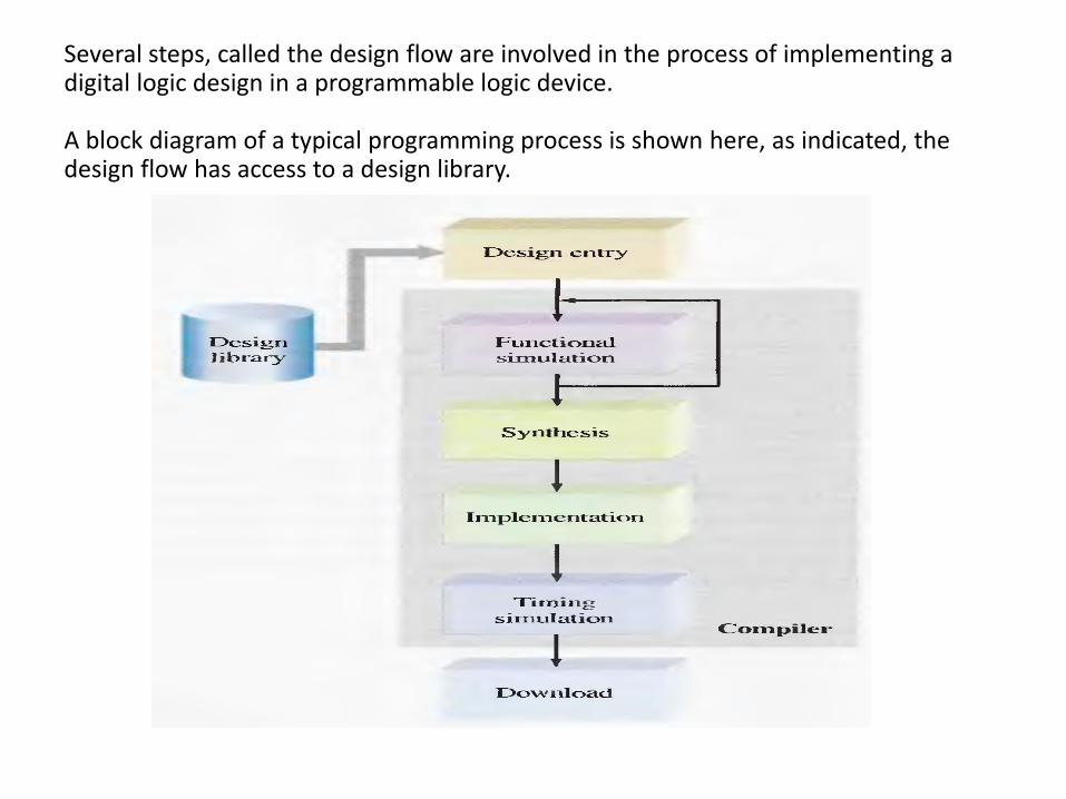
Several steps, called the design flow are involved in the process of implementing a digital logic design in a programmable logic device. A block diagram of a typical programming process is shown here, as indicated, the design flow has access to a design library.

Design Entry: This is the first programming step. The circuit or system design
must be entered into the design application software using text-based entry, graphic entry (schematic capture), or state diagram description. -Design entry is device independent. -Text-based entry is accomplished with a hardware description language (HDL) such as VHDL, Verilog. - Graphic (schematic) entry allows pre-stored logic functions from a library to be selected, placed on the screen, and then interconnected to create a logic design. - State diagram entry requires specification of both the states through which a sequential logic circuit progresses and the conditions that produce each state change.
-Once a design has been entered, it is compiled.
Functional Simulation: The entered and compiled design is simulated by
software to confirm that the logic circuit functions as expected. -The simulation will verify that correct outputs are produced for a specified set of inputs. -A device-independent software tool for doing this is generally called a waveform editor: Any flaws demonstrated by the simulation would be corrected by going back to design entry and making appropriate changes.

Synthesis: Synthesis is where the design is translated into a netlist, which has a
standard form and is device independent. - During the synthesis phase of the design flow, the design is optimized in terms of minimizing the number of gates. replacing logic elements with other logic elements that can perform the same function more efficiently, and eliminating any redundant logic. - The final output from the synthesis phase is a netlist that describes the optimized version of the logic circuit. - A netlist is basically a connectivity list that describes components and how they are connected together.

Implementation: Implementation is where the logic structures described by the
netlist are mapped into the actual structure of the specific device being programmed. The implementation process is called fitting or place and route and results in an output called a bit stream, which is device dependent.
Timing Simulation: This step comes after the design is mapped into the specific
device. The timing simulation is basically used to confirm that there are no design flaws or timing problems due to propagation delays.
Download: Once a bit stream has been generated for a specific programmable
device, it has to be downloaded to the device to implement the software design in hardware.
• An ASIC is basically an integrated circuit designed specifically for a special purpose or application.
• Strictly speaking, this also implies that an ASIC is built only for one and only one customer.
• An example of an ASIC is an IC designed for a specific line of cellular phones of a company, whereby no other products can use it except the cell phones belonging to that product line.
Application Specific Integrated Circuits (ASICSs)

PLDs ASICs
Standard Cell
Full Custom
Gate Arrays
Structured ASICs*
SPLDs
CPLDs
*Not available circa early 1980s
The
GAP
Large Complex Functions . Millions of Gates
Customised for Extremes of Speed, Low Power, Radiation Hard
(Very) Expensive (in small quantities) > $1 Million mask set
(Very) Hard to Design.
Long Design cycles.
NOT Reprogrammable. High Risk
Limited Complexity
Thousands of Gates
Cheap
Easy to Design
Reprogrammable.
Custom Fabricated Design from Scratch
Prefabricated Programmed
PLD Vs ASICS

PLDs ASICs
Standard Cell
Full Custom
Gate Arrays
Structured ASICs*
SPLDs
CPLDs
*Not available circa early 1980s
The
GAP
Large Complex Functions
Inexpensive
Easy to Design
Reprogrammable.
FPGA
Field Programmable Gate Array

• FPGA contain a lot (up to 100000) of tiny blocks of logic with flip-flops, CPLD’“ contain relatively few (a few 100's max) large blocks of logic with flip-flops.
• FPGAs are RAM based - they need to be "downloaded" (configured) at each
power-up. CPLDs are EEPROM based - they are active at power-up (i.e. as long as
they've been programmed at least once...).
• FPGAs have special routing resources to implement efficiently arithmetic
functions (binary counters, adders, comparators...). CPLDs do not.
• CPLDs have a faster input-to-output timings than FPGAs (because of their coarse-
grain architecture.
CPLD Vs FPGA

PLDs are devices whose internal architecture is predetermined by the
manufacturer, but are created in such a way that they can be configured by
engineers in the field to perform a variety of different functions.
In comparison to an FPGA, however, these devices contain a relatively limited
number of logic gates, and the functions they can be used to implement are
much smaller and simpler.
At the other end of the spectrum are ASICs that can contain hundreds of
millions of logic gates and can be used to create incredibly large and complex
functions.
Although ASICs offer the ultimate in size (number of transistors), complexity, and
performance, designing and building one is an extremely time consuming and
expensive process, with the added disadvantage that the final design is frozen
in silicon and cannot be modified without creating a new version of the device.
Thus, FPGAs occupy a middle ground between PLDs and ASICs because their
functionality can be customized in the field like PLDs, but they can contain
millions of logic gates and be used to implement extremely large and complex
functions that previously could be realized using only ASICs.
Why Use FPGA?

When they first arrived on the scene in the mid-1980s, FPGAs were largely used
to implement glue logic, medium-complexity state machines, and relatively limited
data processing tasks.
During the early 1990s, as the size and sophistication of FPGAs started to
increase, their big markets at that time were in the telecommunications and
networking arenas, both of which involved processing large blocks of data and
pushing that data around.
Later, toward the end of the 1990s, the use of FPGAs in consumer, automotive,
and industrial applications underwent a humongous growth spurt.
FPGAs are often used to prototype ASIC designs or to provide a hardware platform
on which to verify the physical implementation of new algorithms.
Some of these devices feature embedded microprocessor cores, high speed
input/output (I/O) devices, and the like.
The result is that today’s FPGAs can be used to implement just about anything,
including communications devices and software-defined radio; radar, image, and
other digital signal processing (DSP) applications; and all the way up to system- on-
chip (SoC) components that contain both hardware and software elements.
Applications
• All FPGAs need to be programmed or configured.
• There are three major circuit technologies for configuring an FPGA:
• SRAM.
• Antifuse.
• Flash.
• FPGAs are chips, which are programmed by the customer to perform the desired functionality. The chips may be programmed either:
• once: Antifuse technology
• several times: Flash based
• dynamically: SRAM based
Programming technologies

• As a diametric alternative to fusible-link technologies, we have their antifuse counterparts, in which each configurable path has an associated link called an antifuse.
• In its un-programmed state, an antifuse has such a high resistance that it may be considered an open circuit (a break in the wire).
• Fig: (a) shows how the device appears when first purchased. However, antifuses can be selectively grown (programmed) by applying pulses of relatively high voltage and current to the de ice’s inputs.
• For example, if we add the antifuses associated with the complementary version of input a and the true version of input b, our device will now perform the function y !a & b Fig: (b).
Antifuse Technology
Fig: (a) Fig: (b)

• Not surprisingly, devices based on antifuse technologies are OTP, because once an antifuse has been grown, it cannot be removed, and there’s no changing your mind.
• Antifuse devices tend to be faster and require lower power.
Antifuse Technology Trade-Offs

• SRAM is currently the dominant FPGA technology.
• The static qualifier associated with SRAM means that—once a value has been loaded into an SRAM cell—it will remain unchanged unless it is specifically altered or until power is removed from the system.
• Consider the symbol for an SRAM-based programmable cell as shown:
• The entire cell comprises a multi-transistor SRAM storage element whose output drives an additional control transistor.
• Depending on the contents of the storage element (logic 0 or logic 1), the control transistor will be either OFF (disabled) or ON (enabled).
SRAM-Based Technology

• SRAM- based FPGAs hold their configurations in static memory. The o/p of the memory cell is directly connected to another circuit and the state of the memory cell controls the circuit being configured.
• Advantages:
• Re-programmable;
• dynamically reconfigurable;
• uses standard processes.
• Disadvantages:
• SRAM burns power.
• Possible to steal, disrupt configuration bits.
• The basic method used to build a combinational logic block (CLB)--- also called a logic element or LE---- in an SRAM-based FPGA is the lookup table (LUT).

• The underlying concept behind a LUT is relatively simple. A group of input signals is used as an index (pointer) to a lookup table.
• The contents of this table are arranged such that the cell pointed to by each input combination contains the desired value.
• For e a ple, let’s assu e that e ish to i ple e t the fu ctio :
LUT based Logic Blocks in SRAM

• This can be achieved by loading a 3-input LUT with the appropriate values.
• A commonly used technique is to use the inputs to select the desired SRAM cell using a cascade of transmission gates.

• If a transmission gate is enabled (active), it passes the signal seen on its input through to its output.
• If the gate is disabled, its output is electrically disconnected from the wire it is driving.
• The transmission gate symbols shown with a small circle indicate that these gates will be activated by a logic 0 on their control input. By comparison, symbols without bobbles indicate that these gates will be activated by a logic 1.
• Based on this understanding, it’s easy to see how different input combinations can be used to select the contents of the various SRAM cells.
• A disadvantage of SRAM-based programmable devices is that each cell consumes a significant amount of silicon real estate because the cells are formed from four or six transistors configured as a latch.
• Another disadvantage is that the de ice’s configuration data (programmed state) will be lost when power is removed from the system, so these devices always have to be reprogrammed when the system is powered on.
• Advantages are that such devices can be reprogrammed quickly and easily, and SRAM uses a standard fabrication technology that is always being improved upon.
SRAM-Based Technology Trade-offs

• A relatively new technology known as FLASH is being used in some FPGAs today.
• This technology grew out of an earlier technology known as erasable
programmable read-only memory (EPROM) that allows devices to be programmed, erased, and reprogrammed with new data.
• In its un-programmed state, as provided by the manufacturer, all of the floating gates in the EPROM transistors are uncharged.
• In this case, placing a row line in its active state will turn on all of the transistors connected to that row, thereby causing all of the column lines to be pulled down to logic 0 via their respective transistors.
FLASH-Based Technology
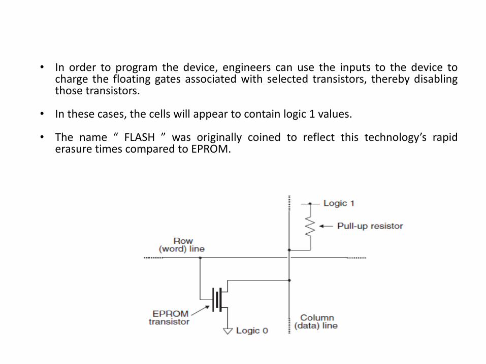
• In order to program the device, engineers can use the inputs to the device to charge the floating gates associated with selected transistors, thereby disabling those transistors.
• In these cases, the cells will appear to contain logic 1 values.
• The name FLASH was originally coined to reflect this tech olog ’s rapid erasure times compared to EPROM.
• FLASH FPGAs are nonvolatile like antifuse FPGAs, but they are also reprogrammable like SRAM FPGAs.
• FLASH FPGAs use a standard fabrication process like SRAM FPGAs and use lower power like antifuse FPGAs.
• FLASH FPGAs are relatively fast.
FLASH-Based Technology Trade-Offs

Goals and Techniques
The logical functions to be performed is only one of the goals that must be met by
FPGA of any digital system design. Many other attributes must be satisfied for the
project to be successful.
• Performance: The logic must run at a required rate.
• Power/Energy: The chip must often run within an energy or power budget.
• Design cost: design cost must be affordable which is directly dependent on
design time.
• Manufacturing cost: the manufacturing cost is the cost of replicating the systems
many times.

Hierarchical Design
Hierarchical design is a standard method for dealing with complex digital designs
• Divide-and-conquer: The procedure’s complexity is conquered by recursively
breaking it down into manageable pieces.
• Group several components into larger components
• Transistor from gates;
• Gates from functional units;
• Functional units from processing elements;
Design Abstraction
• Design Abstraction is critical to hardware system design.
• Hardware designers use multiple levels of design abstraction to manage the
design process and ensure that they meet major design goals, such as speed and
power consumptions.

FPGA Design Abstraction
• Behaviour: A detailed, executable description of what the chip should do, but
not how it should do it.
• Register-transfer: The s ste ’s time behavior is fully specified, but the logic is
not specified as gates.
• Logic: The system is designed in terms of Boolean logic gates, latched, and flip-
flops.
• Configuration: The logic must be placed into logic elements around the FPGA
and the proper connections must be made between the logic elements.
Design Methodologies
• Complex problems can be tackled using methodologies.
• A methodology provides us with a set of guidelines for what to do, when to do it,
and how to know when we are done.
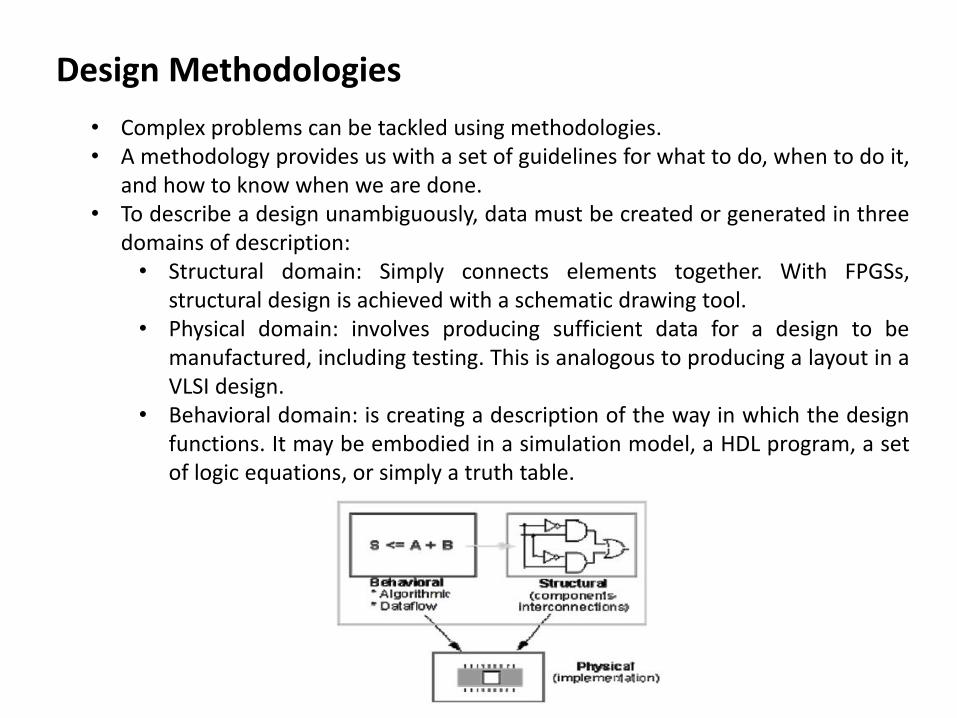
• To describe a design unambiguously, data must be created or generated in three
domains of description:
• Structural domain: Simply connects elements together. With FPGSs,
structural design is achieved with a schematic drawing tool.
• Physical domain: involves producing sufficient data for a design to be
manufactured, including testing. This is analogous to producing a layout in a
VLSI design.
• Behavioral domain: is creating a description of the way in which the design
functions. It may be embodied in a simulation model, a HDL program, a set
of logic equations, or simply a truth table.