Experiments in Computer and Microcontroller Applications
175
Ministry of Higher Education and Scientific Research University of Technology Department of Electrical Engineering Computer and Microcontroller Applications Laboratory Experiments in Computer and Microcontroller Applications By Firas Mohammed Ali Reviewed by Dr. Khalida Sha’ban Rijab Copyright © by the University of Technology, 2013.
Transcript of Experiments in Computer and Microcontroller Applications

Ministry of Higher Education and Scientific Research University of Technology Department of Electrical Engineering Computer and Microcontroller Applications Laboratory
Experiments in
Computer and Microcontroller Applications
By
Firas Mohammed Ali
Reviewed by
Dr. Khalida Sha’ban Rijab Copyright © by the University of Technology, 2013.

Preface Experiments in Computer and Microcontroller Applications is a manual written to cover some practical applications of the 8051 microcontroller. This subject is taught as a lab course to 4th year electronic engineering students at the department of electrical engineering. Each experiment is designed to be a mini-project and contains a theoretical section, typical example programs, procedure, exercises, and discussion problems. The first two experiments are related with the 8086 assembly programming and constitute a continuation to what had been taken by the students about the 8086 microprocessor in the previous courses. This could be a good introduction to the 8051 microcontroller due the similarities between the instruction set of the 8086 microprocessor and that of the 8051 microcontroller. The remaining experiments are based on an 8051 microcontroller trainer kit available at the lab. In each experiment, the student should learn how to interface the main microcontroller trainer board with the relevant application module, write and assemble the control program with a suitable assembler or emulator, and download the program into the 8051 microcontroller to run it. Practicing with more applications would increase the student’s experience and knowledge. This manual can be further enhanced with additional experiments by designing new application modules that can be interfaced with the main microcontroller unit. Finally, I hope that this effort be useful for the electronic engineering students in introducing the subject of 8051 microcontroller system design. Firas M. Ali Baghdad, 2013
i

Acknowledgements
I would like to express my deep gratitude to Dr. Khalida Sha’ban for her continuous support, manuscript review, and scientific notations about the topics, material, and procedures of the experiments in this manual. I would like also to submit my sincere thanks to Mr. Mohammed A. Noaman for providing me with some valuable tutorials and e-books about 8051 microcontroller construction and programming. The useful notes and suggestions of Dr. Eyad I. Abbas and Mr. Hasan M. Azzawi are greatly appreciated. Finally, I am very indebted to Ms. Hiba Faraj for her cooperation in testing and running the programs of the experiments in this manual.
ii

Table of Contents
Subject Page Experiment 1: Debug Programming ………………………………………………..... 1
Experiment 2: Assembly Language Programming …………………………………... 11
Experiment 3: The 8051 Instruction Set and Assembly Programming ……………… 21
Experiment 4: The 8051 Microcontroller Trainer …………………………………… 39
Experiment 5: Interfacing the 8051 Microcontroller with the 7-Segment Display ….. 59
Experiment 6: Stepper Motor Control Using the 8051 Microcontroller …………….. 67
Experiment 7: Digital to Analog Converter Interfacing with the 8051 Microcontroller .....................................................................................
87
Experiment 8: Analog to Digital Converter Interfacing with the 8051 Microcontroller .....................................................................................
101
Experiment 9: DC Motor Speed Control Using the 8051 Microcontroller …………... 111
Experiment 10: 8051 Microcontroller-Based System Design ……………………….. 117
References …………………………………………………………………………… 125
Appendix-A: The 8051 Microcontroller Architecture ………………………………. 127
Appendix-B: The MIDE-51 Tutorial ………………………………………………… 147
Appendix-C: MCU 8051 IDE Tutorial ………………………………………………. 151
Appendix-D: Alphabetical List of the 8051 Instructions ……………………………. 167
iii

Experiment 1 Debug Programming
Experiment 1
DEBUG Programming Objectives The purpose of this experiment is to learn using Debug program in executing assembly language instructions. 1. Theory DEBUG is a program included in the MS-DOS and Windows operating systems which allows the assembly language programmer to monitor the program execution closely for debugging purposes. Specifically, it can be used to examine and alter the contents of memory, to enter and run assembly programs, and to stop programs at certain points in order to check or change data. 1.1 Entering and Exiting DEBUG To enter the DEBUG program from Windows XP, click on Start button, select Programs, and Accessories, and then Command Prompt as follows: Start Programs Accessories Command Prompt The MS-DOS command prompt window will be opened. To enter the DEBUG program, simply type DEBUG at the DOS command prompt: C:\> DEBUG - "DEBUG" may be typed in either uppercase or lower case.
Figure 1: The DEBUG Window
- 1 -

Experiment 1 Debug Programming
To exit DEBUG and return to MS-DOS command window, use the quit command (Q) as follows: - Q C:\>- Note: To return into the Windows operating system, type the command exit at the MS-DOS
command prompt. 1.2 Displaying and Altering the Contents of Registers The register command (R) allows you to examine or alter the contents of the internal registers of the CPU. It has the following syntax: - R <register name> The R command will display all registers unless the optional field <register name> is entered, in which case only the register named will be displayed. Example 1: Use the R command to display all registers. - R AX=0000 BX=0000 CX=0000 DX=0000 SP=FFEE BP=0000 SI=0000 DI=0000 DS=0C44 ES=0C44 SS=0C44 CS=0C44 IP=0100 NV UP DI PL NZ NA PO NC 0C44:0100 0000 DEC BP - When you enter DEBUG initially, the general-purpose registers are set to zero and the flag bits are reset. The contents of the segment registers will vary depending on the operating system you are using. Example 2: Use the R command to display and modify the content of register CX. - R CX CX 0000 : The new value of CX can be entered at the displayed colon. : 44FF Note that the program DEBUG displays the contents of registers in Hexadecimal format. 1.3 Coding and Running Assembly Programs in Debug There are certain commands that can be used to enter simple assembly language instructions, and assemble and run them.
- 2 -

Experiment 1 Debug Programming
These commands include the assemble (A) command, the unassembled (U) command, the go (G) command, and the trace (T) command. 1.3.1 The Assemble (A) Command The assemble command is used to enter Assembly language instructions into memory. It takes the following syntax: - A <starting address> The starting address may be given as an offset number which is the starting address of the code segment. After the A command is entered, the DEBUG program will prompt you to enter the assembly language instructions. The logical address for each instruction (CS:IP) is displayed automatically by the DEBUG program. Example 3: Enter the following assembly language instructions into the DEBUG program: MOV AX,05 MOV BX,03 MOV CX,0C ADD AX,BX ADD AX,CX INT 3 The steps for entering the above instructions are shown below: C:\>DEBUG -A 100 0B0B:0100 MOV AX,05 0B0B:0103 MOV BX,03 0B0B:0106 MOV CX,0C 0B0B:0109 ADD AX,BX 0B0B:010B ADD AX,CX 0B0B:010D INT 3 0B0B:010E After each instruction is entered, the enter key should be pressed. To stop entering instructions, press the enter key. In this example the starting address of the program is 100H, which is the content of the instruction pointer (IP). The value 0B0BH shown in the program represents the content of the code segment register (CS). This value is set by the operating system (OS). Note: There is no need to type the letter H after numbers entered in hexadecimal format since
DEBUG assumes that all numbers are in hexadecimal system. 1.3.2 The Unassemble (U) Command The unassemble command (U) displays the machine code in memory along with their equivalent Assembly language instructions. It takes the following syntax:
- 3 -

Experiment 1 Debug Programming
- U <starting address> <ending address> Example 4: Use the U command to display the machine code of the program entered in
example 3 above. The unassemble command can be written as shown below: -U 100 10D 0B0B:0100 B80500 MOV AX,0005 0B0B:0103 BB0300 MOV BX,0003 0B0B:0106 B90C00 MOV CX,000C 0B0B:0109 01D8 ADD AX,BX 0B0B:010B 01C8 ADD AX,CX 0B0B:010D CC INT 3 - In this case, the starting address is 100H and the ending address is 10DH. After typing the U command, the enter key should be pressed to display the machine code in hexadecimal format. 1.3.3 The Go (G) Command (Run Command) The go (G) command is used to execute the Assembly language instructions entered to DEBUG. Its format is: - G = <starting address> <stop address> After executing the instructions, the G command displays the contents of all CPU registers. Example 5: Execute the program of example 3 using the G command. The program is executed as follows: - G = 0100 010E AX=0014 BX=0003 CX=000C DX=0000 SP=FFEE BP=0000 SI=0000 DI=0000 DS=0B0B ES=0B0B SS=0B0B CS=0B0B IP=010D NV UP EI PL NZ AC PE NC 0B0B:010D CC INT 3 - 1.3.4 The trace (T) command This is a powerful debugging command which allows tracing through the execution of the program one instruction at a time to verify the effect of the program on registers and memory locations. The syntax of the T command is: - T = <starting address> <number of instructions>
- 4 -

Experiment 1 Debug Programming
The difference between this command and the go command is that T command will display the register contents after each instruction, whereas the G command does not display them until after termination of the program. Example 6: Execute the previous program using the T command after resetting the contents
of registers AX, BX, and CX. The T command is written as shown below: -T = 100 5 AX=0005 BX=0000 CX=0000 DX=0000 SP=FFEE BP=0000 SI=0000 DI=0000 DS=0B0B ES=0B0B SS=0B0B CS=0B0B IP=0103 NV UP EI PL NZ NA PO NC 0B0B:0103 BB0300 MOV BX,0003 AX=0005 BX=0003 CX=0000 DX=0000 SP=FFEE BP=0000 SI=0000 DI=0000 DS=0B0B ES=0B0B SS=0B0B CS=0B0B IP=0106 NV UP EI PL NZ NA PO NC 0B0B:0106 B90C00 MOV CX,000C AX=0005 BX=0003 CX=000C DX=0000 SP=FFEE BP=0000 SI=0000 DI=0000 DS=0B0B ES=0B0B SS=0B0B CS=0B0B IP=0109 NV UP EI PL NZ NA PO NC 0B0B:0109 01D8 ADD AX,BX AX=0008 BX=0003 CX=000C DX=0000 SP=FFEE BP=0000 SI=0000 DI=0000 DS=0B0B ES=0B0B SS=0B0B CS=0B0B IP=010B NV UP EI PL NZ NA PO NC 0B0B:010B 01C8 ADD AX,CX AX=0014 BX=0003 CX=000C DX=0000 SP=FFEE BP=0000 SI=0000 DI=0000 DS=0B0B ES=0B0B SS=0B0B CS=0B0B IP=010D NV UP EI PL NZ AC PE NC 0B0B:010D CC INT 3 - Note: The contents of registers can be reset by using the R command followed by the desired
register. 1.4 Data Manipulation in DEBUG There are some commands that are used to examine and alter the contents of memory. These are: F: The Fill command which is used to fill a block of memory with data. D: The Dump command which displays contents of memory to the screen. E: The Enter command which is used to alter the contents of memory. 1.4.1 The Fill (F) Command The fill command is used to fill an area of memory with same data items. The syntax of the F command is as follows: - F <starting address> <ending address> <data>
- 5 -

Experiment 1 Debug Programming
In this case the start and end addresses are offset addresses in the data segment. To fill other segments with data, the segment register should precede the starting offset address. For example to fill a block in the code segment, the syntax becomes: - F CS:<starting address> <ending address> <data> And to fill a block in the stack segment, the syntax is: - F SS:<starting address> <ending address> <data> This command is useful for initializing a certain block of memory with data, for example initializing an area of memory with zeros. Example 7: The following command resets the first ten memory locations in the data segment. - F 00 09 00 Example 8: The following command sets the first 16 memory locations in the stack to FFH. - F SS:00 0F FF Note: The size of each memory location is one byte. 1.4.2 The Dump (D) Command The D command is used to display the contents of memory between a start and an end address. Its syntax is: - D <start address> <end address> As in the case of the fill command, the start and end addresses are offset addresses in the data segment. To display data in other segments, the segment register should precede the starting offset address. Example 9: Assemble and run the following program. Examine the content of memory location 100 in the data segment after program execution. MOV AX, 2020 MOV DS, AX MOV AL, 57 MOV [100], AL HLT The steps of executing and examining the above program are as follows. C:\>DEBUG -A 100 0B0B:0100 MOV AX, 2020
- 6 -

Experiment 1 Debug Programming
0B0B:0103 MOV DS, AX 0B0B:0105 MOV AL, 57 0B0B:0107 MOV [100], AL 0B0B:010A HLT 0B0B:010B -G = 0100 010B AX=2057 BX=0000 CX=0000 DX=0000 SP=FFEE BP=0000 SI=0000 DI=0000 DS=2020 ES=0B0B SS=0B0B CS=0B0B IP=010B NV UP EI PL NZ NA PO NC -D 100 100 2020:0100 57 - As shown from the DEBUG screen, the content of memory location DS:100 is 57H. The logical address of this location is 2020:0100. In this case, the start address equals the stop address (one memory location). 1.4.3 The Enter (E) Command The fill command was used to fill a memory block with the same memory items. The E command can be used to enter a list of data into a certain portion of memory. The syntax is: - E <start address> <data list> Example 10: Use the E command to enter the data list (25 12 15 1F 2B) at the memory locations starting from offset address 200H to offset 204H in the data segment. Verify the entered data using the D command. C:\>DEBUG -E 200 25 12 15 1F 2B -D 200 204 0B0B:0200 25 12 15 1F 2B - 2. Procedure Implement the examples presented in section 1 above using the Debug program. For Windows -64 bits, use the DOSBOX utility to make a virtual environment for Debug.
- 7 -

Experiment 1 Debug Programming
3. Exercises Exercise 1: Assemble, unassemble, and run the following assembly program with DEBUG and monitor the contents of registers AX and BX after execution. MOV AL,76 MOV BH,8F ADD BH,AL ADD BH,7B MOV BL,BH ADD BL,AL MOV AH,BL
Exercise 2: Use DEBUG to enter the data array [12 38 25 0C 3A] into memory locations with offsets from 0200 to 0204 in the data segment, then execute the following assembly instructions: MOV AL,00 MOV SI,200 ADD AL,[SI] ADD AL,[SI+1] ADD AL,[SI+2] ADD AL,[SI+3] ADD AL,[SI+4] HLT
Exercise 3: Display the contents of memory locations from 0100 to 0105 in the stack after executing the following assembly instructions: MOV SP, 0106 MOV AX, 24B6 MOV BX, 85C2 MOV DX, 5F93 PUSH AX PUSH BX PUSH DX HLT
4. Discussion 1- What are the main advantages of using DEBUG in executing assembly language
instructions? 2- Find the content of the stack and the stack pointer after the execution of the following
instructions. Write the necessary DEBUG command for displaying the stack content.
MOV SP,2000 MOV AX,3291 MOV BX,4F3C
- 8 -
Experiment 1 Debug Programming
MOV CX,0009 PUSH AX PUSH BX PUSH CX
3- Write the DEBUG commands necessary to do the following:
• Execute 3 instructions of a program with a start address of 100H. • Fill memory locations 200H and 201H with the values 2CH and 3AH. • Display memory contents between offset 300H and 306H. • Display the stack contents between offset 500H and 510H.
4- Sketch the memory map of the stack after executing the following assembly program:
MOV AX, 3020H MOV BX, 5025H MOV SP, 200AH PUSH BX PUSH AX
Assume that the content of the stack segment register is 8000H. 5- Use DEBUG to write and execute a program for doing the following tasks:
1. Loading register AX with the value 99H 2. Loading register BX with the value 25H. 3. Adding the contents of AX and BX and saving the result in AX. 4. Transferring the result into memory location 400H. 5. Initializing the stack pointer with the value 500H. 6. Pushing the content of AX into the stack.
Execute the program and display the memory content of location 400H and the stack. 6- Write an assembly program to load register CX with 2578H, and register DX with 3A2CH
and exchange data between them using the PUSH and POP instructions.
- 9 -

Experiment 1 Debug Programming
This page is left intentionally blank
- 10 -
Experiment 2 Assembly Language Programming
Experiment 2
Assembly Language Programming Objectives
The purpose of this experiment is to learn writing, assembling, and running typical assembly language programs using a commercial assembler. 1. Introduction Practical assembly language programs can, in general, be written using one of the two following methods:
1- The full-segment definition form 2- The simplified segment definition form
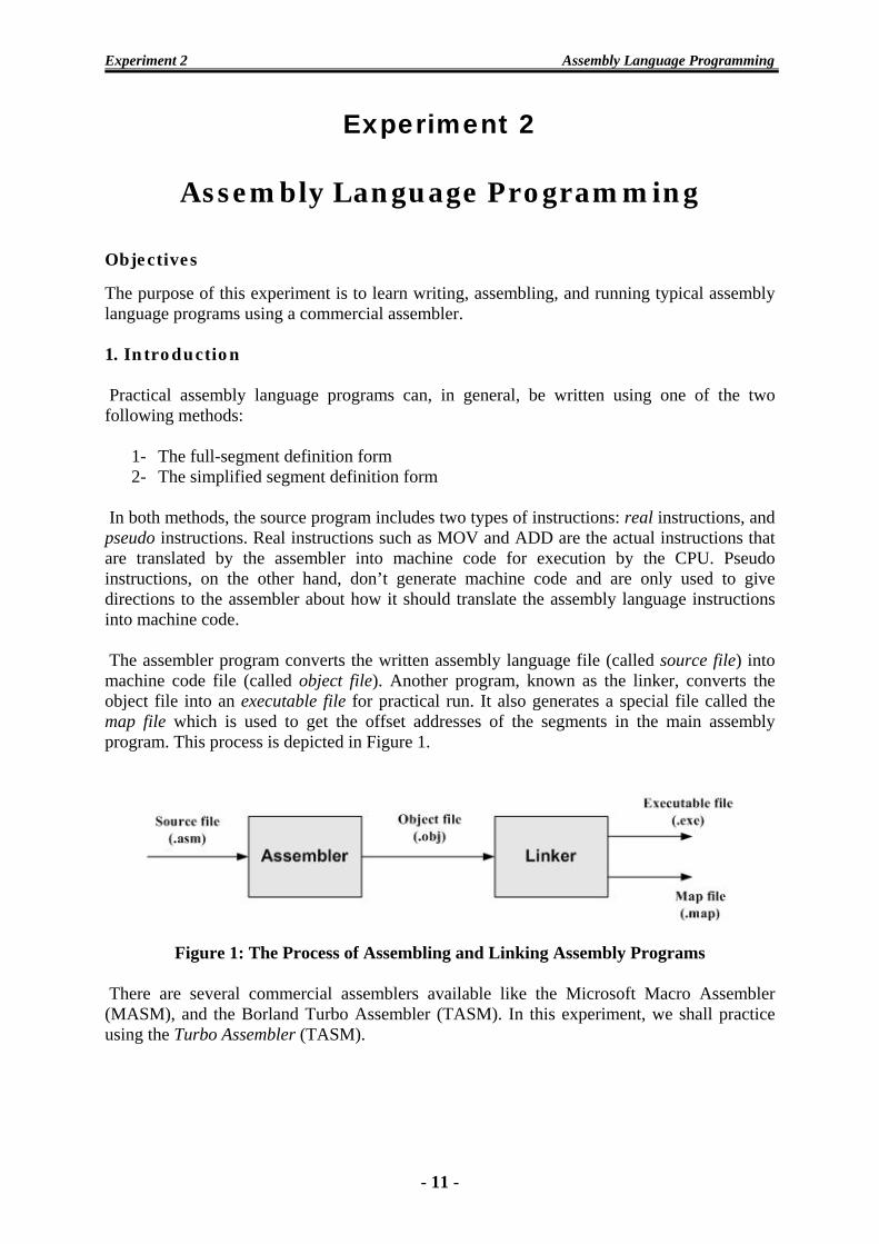
In both methods, the source program includes two types of instructions: real instructions, and pseudo instructions. Real instructions such as MOV and ADD are the actual instructions that are translated by the assembler into machine code for execution by the CPU. Pseudo instructions, on the other hand, don’t generate machine code and are only used to give directions to the assembler about how it should translate the assembly language instructions into machine code. The assembler program converts the written assembly language file (called source file) into machine code file (called object file). Another program, known as the linker, converts the object file into an executable file for practical run. It also generates a special file called the map file which is used to get the offset addresses of the segments in the main assembly program. This process is depicted in Figure 1.
Figure 1: The Process of Assembling and Linking Assembly Programs There are several commercial assemblers available like the Microsoft Macro Assembler (MASM), and the Borland Turbo Assembler (TASM). In this experiment, we shall practice using the Turbo Assembler (TASM).
- 11 -

Experiment 2 Assembly Language Programming
2. Full Segment Definition Form Although one can write an assembly language program that uses only one segment, normally a program consists of three segments: the stack segment, the data segment, and the code segment. Figure 2 presents a sample shell of an assembly language program. The TITLE pseudo-instruction at the beginning of the program is optional and is used to write comments about the purpose of the program. The program consists of three segments. The SEGMENT and ENDS pseudo instructions indicate to the assembler the beginning and ending of a segment and have the following format: Label SEGMENT ; place the statements of this segment Label ENDS The ENDS label must be the same label as in the SEGMENT pseudo-instruction.
Figure 2: Standard Full Segment Definition Form of the Assembly Language Program The stack segment in Figure 2 contains one line, DB 64 DUP(?). This pseudo instruction reserves 64 bytes of memory for the stack. The data segment is used to define and reserve data in memory that can be used later in the code segment. There are several pseudo instructions for data allocation and definition in the data segment. The ASSUME pseudo instruction at the beginning of the code segment associates segment registers with specific segments by assuming that the segment register is equal to the segment labels used in the program. The operating system must pass control to the program so that it may execute, but before that it assigns values for the segment registers. Upon taking control from the operating system, the segment registers CS and SS have their proper values. The DS value must be initialized by the program. This is done as follows:
- 12 -
Experiment 2 Assembly Language Programming
MOV AX,DTSEG MOV DS,AX Two lines of code are used because segment registers can not be loaded directly. The last two instructions in the code segment are: MOV AH,4CH INT 21H Their purpose is to return control to the operating system. The END pseudo instruction ends the entire program. 2.1 Assembler Data Pseudo Instructions The assembler supports all the various data types of the 8086 microprocessor by providing data pseudo-instructions that define the data types and set aside memory for them. The following are some of the most widely used data definition pseudo instructions: ORG (Origin) ORG is used to indicate the beginning of the offset address. The number that comes after ORG can be either in hex or in decimal. DB (Define Byte) The DB pseudo-instruction is one of the most widely used data pseudo instructions in the assembler. It allows allocation of memory in byte-sized locations. This is the smallest allocation unit permitted. DB can be used to define numbers in decimal, binary, hex, and ASCII. Following are some DB examples: A1 DB 25 ; Decimal A2 DB 10010001B ; Binary A3 DB 12H ; HEX ORG 10H A4 DB ‘Name’ ; ASCII Characters DUP (Duplicate) DUP is used to duplicate a given number of characters. This can avoid a lot of typing. For example, note the following two methods of filling six memory locations with FFH: Array1 DB 0FFH, 0FFH, 0FFH, 0FFH, 0FFH, 0FFH ORG 20H Array2 DB 6 DUP(0FFH) The following example reserves 64 bytes of memory with no initial value given and starting from offset address 50H: ORG 50H Array3 DB 64 DUP (?)
- 13 -

Experiment 2 Assembly Language Programming
DW (Define Word) DW is used to allocate memory 2 bytes (one word) at a time. The following are some examples: DATA1 DW 253FH Y DW 3AC4H, 6080H, 2FF5H X DW 8 DUP(?) EQU (Equate) This pseudo instruction is used to define a constant without occupying a memory location. EQU does not set aside storage for a data item but associates a constant value with a data label so that when the label appears in the program its constant value will be substituted for the label. For example: COUNT EQU 20 Example 1: Write an assembly program to add two values of size 1 byte, and save the sum
in certain memory location. Use the standard full segment definition form. Solution: TITLE Program to add two hex numbers STSEG SEGMENT DB 64 DUP(?) STSEG ENDS DTSEG SEGMENT X1 DB 25H X2 DB 34H SUM DB ? DTSEG ENDS CDSEG SEGMENT ASSUME CS:CDSEG,DS:DTSEG,SS:STSEG MOV AX,DTSEG MOV DS,AX MOV AL,X1 MOV BL,X2 ADD AL,BL MOV SUM,AL MOV AH,4CH INT 21H CDSEG ENDS END
- 14 -

Experiment 2 Assembly Language Programming
3. Simplified Segment Definition Form The simplified segment definition form, or simplified format, for writing assembly programs is much easier to understand and use than the full segment definition form. It is supported by latest versions of assemblers. Before using the simplified segment definition, the memory model for the program must be chosen. There are four memory models SMALL, MEDIUM, COMPACT, and LARGE. SMALL MODEL: This is one of the most widely used memory models for assembly language programs and is sufficient for most programs. The SMALL model uses a maximum of 64KB of memory for code and another 64KB for data. MEDIUM MODEL: In this model, the data segment must fit into 64KB, but the code segment can exceed 64KB of memory. COMPACT MODEL: This is the opposite of the MEDIUM model. While the data segment can exceed 64KB of memory, the code segment cannot. LARGE MODEL: Combining the two preceding models gives the LARGE model. This allows the data and code segments to exceed 64KB of memory. The simplified segment definition format uses three simple pseudo-instructions to define segments. These are .CODE, .DATA, and .STACK, which correspond to the code, data, and stack segments respectively. Using this method makes the SEGMENT and ENDS pseudo instructions unnecessary. Figure 3 shows the format of the simplified segment definition method.
Figure 3: The Simplified Format for the Assembly Program File Example 2: Write the program of example 1 using the simplified segment definition
format.
- 15 -

Experiment 2 Assembly Language Programming
Solution: TITLE Program to add two hex numbers .MODEL SMALL .STACK 64 .DATA X1 DB 25H X2 DB 34H SUM DB ? .CODE MOV AX,@DATA MOV DS,AX MOV AL,X1 MOV BL,X2 ADD AL,BL MOV SUM,AL MOV AH,4CH INT 21H END 4. Using TASM for Assembling Programs In this section we will demonstrate the process of writing, assembling, linking, and running assembly programs using Borland’s Turbo Assembler which runs under DOS. From the start button, select Programs, Accessories, and run the Command Prompt window. Use Alt+Enter keys to open full screen. The DOS command CD\ will transfer you to the root directory of drive C:, while the command CLS will clear the screen. To change to the TASM folder (directory), type the command CD TASM. C:\> CD TASM The source file (Assembly program) must first be written using a text editor such as notepad or MS-DOS Edit program. This can be done by typing the command notepad, or EDIT followed by the source file name and extension: C:\TASM> EDIT prog1.asm C:\TASM> notepad prog1.asm
- 16 -

Experiment 2 Assembly Language Programming
Figure 4: The Notepad Text Editor Window After saving the source file with the correct extension, it can then be assembled to produce the object file. This can be done by invoking the TASM assembly program as follows: C:\TASM>tasm prog1.asm If the source file is free of syntax errors, then the object file prog1.obj will be produced. This file can be used to create the executable file with the aid of the Turbo linker (TLINK) as shown below: C:\TASM>tlink prog1.obj The linker will produce a map file (prog1.map) in addition to the executable file (prog1.exe). This file is necessary to get the start and stop address for each segment in the program. C:\TASM>notepad prog1.map
Figure 5: Editing the Map File
- 17 -

Experiment 2 Assembly Language Programming
In this case the start address of the code segment is 50H, and the stop address is 64H. The four generated files can be listed using the dir DOS command: C:\TASM>dir prog1.* To run the executable file using DEBUG program, the following command should be used: C:\TASM>debug prog1.exe To display the assembly file in the debug environment, the U command is used as follows: - U CS: 50 64 1797:0050 B89B17 MOV AX,179B 1797:0053 8ED8 MOV DS,AX 1797:0055 A00000 MOV AL,[0000] 1797:0058 8A1E0100 MOV BL,[0001] 1797:005C 02C3 ADD AL,BL 1797:005E A20200 MOV [0002],AL 1797:0061 B44C MOV AH,4C 1797:0063 CD21 INT 21 - Note that labels appear as addresses in the debug environment. To run the program, use the G command after determining the start and stop offset addresses: - G = 50 63 In order to check the result, the D command can be used to display data in the data segment. It should be noted that the data segment contains 3 locations (the first 3 bytes are reserved). Thus, the D command is typed as shown below: - D DS:00 02 179B:0000 25 34 59 Which confirms that the result is 59H and is stored at the 3rd location of the data segment. Example 3: Write and run an assembly program that transfers 6 bytes of data from memory
locations with offset of 0010H to memory locations with offset address of 0030H in the data segment. Use the simplified segment definition format.
Solution: TITLE PROGRAM TO TRANSFER 6 BYTES OF DATA .MODEL SMALL .STACK 32 .DATA ORG 10H A DB 25H,4FH,85H,1FH,2BH,0C4H ORG 30H
- 18 -

Experiment 2 Assembly Language Programming
B DB 6 DUP(?) COUNT EQU 06 .CODE MOV AX,@DATA MOV DS,AX MOV SI,OFFSET A MOV DI,OFFSET B MOV CX,COUNT START: MOV AL,[SI] MOV [DI],AL INC SI INC DI DEC CX JNZ START MOV AH,4CH INT 21H END The pseudo instruction OFFSET is used to obtain the offset address of data elements in the data segment. The program can be assembled, linked, and run using the same steps indicated previously. 5. Procedure Implement the examples presented above using the TASM assembler, and run them with the aid of the Debug program. 6. Exercises Exercise 1: Write, assemble, and run a program that adds 5 bytes of data and saves the
result. The data should be the following hex numbers: 25H, 12H, 15H, 1FH, and 2BH. Use the full segment definition model.
Exercise 2: Assume that there is a class of five students with the following grades: 69, 87,
96, 45, and 75. Write and run an assembly program to find the highest grade and save it in certain memory location. Use the full segment definition model.
Exercise 3: Write and run an assembly program that counts the number of ones in a 16-bit
word. Save the result in a memory location named COUNT. Use the simplified segment definition model.
7. Discussion 1. What is the purpose of pseudo-instructions, and how do they differ from real instructions? 2. What is the difference between the source file and the object file? Which program converts
between them? 3. What is the function of the linker program?
- 19 -
Experiment 2 Assembly Language Programming
4. Find the errors in the following assembly program and re-write it correctly:
STAKSG SEGMENT DB 100 DUP(?) STA_SG ENDS DTSEG SEGMENT DATA1 DB ? DTSEG END CDSEG SEGMENT MOV AX,DATSEG MOV DS,AX MOV AL,34H ADD AL,4FH MOV DATA1,AL CDSEG ENDS END
5. Write an assembly program that adds four words of data and save the result in memory. Assume the values are: 234DH, 1DE6H, 3BC7H, and 566AH. Use the simplified segment definition model.
6. Assume that there is a class of ten students with the following grades: 77, 46, 50, 36, 56,
68, 40, 63, 70, 29. Write a program to find the number of passed students and save the result in memory. Use the simplified segment definition model.
7. What is the difference between the following two instructions: (a) MOV BX,DATA1 (b) MOV BX,OFFSET DATA1 8. How many bytes are defined by the following pseudo instruction?
DATA1 DB 6 DUP (4 DUP(0FFH))
- 20 -

The 8051 Microcontroller Instruction Set and Assembly Programming
Experiment 3
Experiment 3
The 8051 Microcontroller Instruction Set and Assembly Programming
Objectives To study the instruction set of the 8051 microcontroller, its addressing modes, and how to write and execute simple assembly programs.
1. The 8051 Instruction Set
The process of writing program for the microcontroller mainly consists of giving instructions (commands) in the specific order in which they should be executed in order to carry out a specific task. All commands are known as INSTRUCTION SET. All microcontrollers compatible with the 8051 have in total of 255 instructions, i.e. 255 different words available for program writing. Depending on operation they perform, all instructions are divided in several groups:
• Data Transfer Instructions • Arithmetic Instructions • Branch Instructions • Logic Instructions • Bit-oriented Instructions
2. The 8051 Addressing Modes
The CPU can access data in various ways. The data could be in a register, or in memory, or be provided as an immediate value. These various ways of accessing data are called addressing modes. The 8051 provides a total of six distinct addressing modes. They are as follows:
1. Immediate Addressing Mode 2. Register Addressing Mode 3. Direct Addressing Mode 4. Indirect Addressing Mode 5. External Indirect Addressing Mode 6. Indexed Addressing Mode
2.1 Immediate Addressing Mode
Immediate addressing is so-named because the value to be stored in memory immediately follows the operation code in memory. That is to say, the instruction itself dictates what value will be stored in memory.
- 21 -
The 8051 Microcontroller Instruction Set and Assembly Programming
Experiment 3
For example, the instruction:
MOV A, #20H
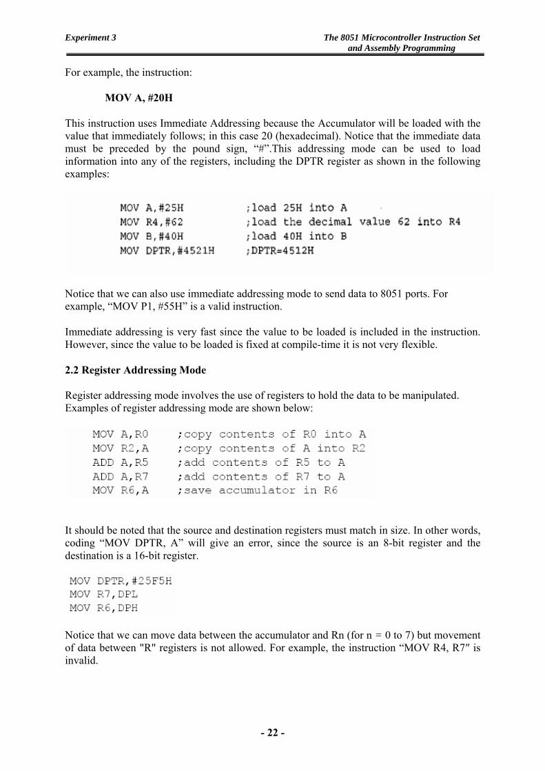
This instruction uses Immediate Addressing because the Accumulator will be loaded with the value that immediately follows; in this case 20 (hexadecimal). Notice that the immediate data must be preceded by the pound sign, “#”.This addressing mode can be used to load information into any of the registers, including the DPTR register as shown in the following examples:
Notice that we can also use immediate addressing mode to send data to 8051 ports. For example, “MOV P1, #55H” is a valid instruction.
Immediate addressing is very fast since the value to be loaded is included in the instruction. However, since the value to be loaded is fixed at compile-time it is not very flexible.
2.2 Register Addressing Mode
Register addressing mode involves the use of registers to hold the data to be manipulated. Examples of register addressing mode are shown below:
It should be noted that the source and destination registers must match in size. In other words, coding “MOV DPTR, A” will give an error, since the source is an 8-bit register and the destination is a 16-bit register.
Notice that we can move data between the accumulator and Rn (for n = 0 to 7) but movement of data between "R" registers is not allowed. For example, the instruction “MOV R4, R7″ is invalid.
- 22 -

The 8051 Microcontroller Instruction Set and Assembly Programming
Experiment 3
2.3 Direct Addressing Mode
Direct addressing is so-named because the value to be stored in memory is obtained by directly retrieving it from another memory location. For example:
MOV A, 30H
This instruction will read the data out of Internal RAM address 30 (hexadecimal) and store it in the Accumulator. Further examples of the direct addressing mode are shown below:
Direct addressing is generally fast since, although the value to be loaded isn't included in the instruction, it is quickly accessible since it is stored in the 8051s Internal RAM. It is also much more flexible than Immediate Addressing Mode since the value to be loaded is whatever is found at the given address. Also, it is important to note that when using direct addressing any instruction which refers to an address between 00H and 7FH is referring to Internal Memory. Any instruction which refers to an address between 80H and FFH is referring to the SFR control registers that control the 8051 microcontroller itself. For example, the instruction MOV 0E0,#30H is equivalent to MOV A,#30H.
2.4 Indirect Addressing Mode
Indirect addressing is a very powerful addressing mode which in many cases provides an exceptional level of flexibility. Indirect addressing is also the only way to access the extra 128 bytes of Internal RAM found on an 8052.
Indirect addressing appears as follows:
MOV A,@R0
- 23 -
The 8051 Microcontroller Instruction Set and Assembly Programming
Experiment 3
This instruction causes the 8051 to analyze the value of the R0 register. The 8051 will then load the accumulator with the value from Internal RAM which is found at the address indicated by R0.
If the data is inside the on-chip RAM, only registers R0 and R1 are used as pointers. In other words, R2 – R7 cannot be used to hold the address of an operand located in RAM when using this addressing mode.
Indirect addressing mode always refers to Internal RAM; it never refers to an SFR.
2.5 External Indirect Addressing Mode
In addition to its code memory, the 8051 family also has 64K bytes of data memory space. In other words, the 8051 has 128K bytes of address space of which 64K bytes are set aside for program code and the other 64K bytes are set aside for data. Program space is accessed using the program counter (PC) to locate and fetch instructions, but the data memory space is accessed using the DPTR register and an instruction called MOVX, where X stands for external (meaning that the data memory space must be implemented externally).
This method of addressing is used to access data stored in external data memory. There are only two commands that use external indirect addressing mode:
MOVX A, @DPTR MOVX @DPTR, A
As you can see, both commands utilize DPTR. In these instructions, DPTR must first be loaded with the address of external memory that you wish to read or write. Once DPTR holds the correct external memory address, the first command will move the contents of that external memory address into the Accumulator. The second command will do the opposite: it will allow you to write the value of the Accumulator to the external memory address pointed to by DPTR.
2.6 Indexed Addressing Mode
Indexed addressing mode is widely used in accessing data elements of look-up table entries located in the program ROM space of the 8051. The instruction used for this purpose is:
“MOVC A, @A+DPTR”
The 16-bit register DPTR and register A are used to form the address of the data element stored in on-chip ROM. Because the data elements are stored in the program (code) space ROM of the 8051, the instruction MOVC is used instead of MOV. The “C” means code. In this instruction the contents of A are added to the 16-bit register DPTR to form the 16-bit address of the needed data.
One major difference between the code space and data space is that, unlike code space, the data space cannot be shared between code and data.
- 24 -

The 8051 Microcontroller Instruction Set and Assembly Programming
Experiment 3
3. Some Specific Instructions
In order to write simple assembly programs for the 8051 microcontroller, certain widely used instructions are explored. These instructions are belonging to the different groups of instruction types illustrated above.
3.1 The MOV Instruction
The MOV instruction is a data transfer instruction, and copies data from one location to another. It has the following format:
MOV destination, source ; copy source to destination.
This instruction tells the CPU to move (in reality, copy) the source operand to the destination operand.
For example, the instruction “MOV A, R0” copies the contents of register R0 to register A. After this instruction is executed, register A will have the same value as register R0. The MOV instruction does not affect the source operand.
When programming the 8051 microcontroller, the following points should be noted:
1. Values can be loaded directly into any of registers A, B, or R0 – R7. However, to indicate that it is an immediate value it must be preceded with a pound sign (#). For example the instruction MOV A,#23H and MOV R5,#0F9H. Notice in instruction “MOV R5 , #0F9H” that a 0 is used between the # and F to indicate that F is a hex number and not a letter. In other words “MOV R5 , #F9H” will cause an error.
2. If values 0 to F are moved into an 8-bit register, the rest of the bits are assumed to be all zeros. For example, in the instruction “MOV A, #5″ the result will be A = 05; that is, A = 00000101 in binary.
3. Moving a value that is too large into a register will cause an error. For example the instruction MOV A,#7F2H is illegal.
3.2 The ADD Instruction
The ADD instruction is an arithmetic instruction. It has the following format: ADD A, source ; ADD the source operand to the accumulator
The ADD instruction tells the CPU to add the source byte to register A, and put the result in register A. The source operand can be either a register or immediate data, but the destination must always be the accumulator (Register A).
For example the following instructions add the contents of register A and register R2 and put the result in the accumulator.
- 25 -

The 8051 Microcontroller Instruction Set and Assembly Programming
Experiment 3
MOV A,#25H ; load 25H into A MOV R2,#34H ; load 34H into R2 ADD A,R2 ; add R2 to accumulator
3.3 The INC Instruction
The INC instruction is an arithmetic instruction, and is used to increment the contents of a register or memory location by 1. For example: INC A, INC R0, INC 7H, INC DPTR.
3.4 The DEC Instruction
The DEC instruction is an arithmetic instruction, and is used to decrement the contents of a register or memory location by 1. For example: DEC A, DEC R1, DEC @R0. The DEC instruction can not be used to decrement the contents of the data pointer register DPTR.
3.5 The DJNZ Instruction
The DJNZ is an important conditional jump instruction that is widely used for making loops in the 8051 programs. This instruction takes the following syntax:
DJNZ register, label
The DJNZ informs the CPU to decrease the content of the register and jump to a specified location in the program determined by the label if the register content is not zero. The program jump will be within –128 to +127 locations relative to the following instruction.
3.6 The SJMP (Short Jump) Instruction
The SJMP instruction is a 2-byte unconditional jump instruction which is used to make jumps in the program. The jump to the target address will be within -128 to +127 bytes of memory relative to the address of the current PC (program counter). The syntax of the SJMP instruction is:
SJMP label
The target address is referred to by the label.
3.7 The LJMP (Long Jump) Instruction
The LJMP instruction is a 3-byte unconditional jump instruction which is used to make jumps in the program. The target address allows a jump to any memory location from 0000 to FFFFH within the 64KB memory address space. The syntax of the LJMP instruction is:
LJMP label
The target address is referred to by the label.
- 26 -

The 8051 Microcontroller Instruction Set and Assembly Programming
Experiment 3
3.8 The JNZ Instruction (Jump if A ≠ 0)
In this instruction the content of register A is checked. If it is not zero, it jumps to the target address. Notice that the JNZ instruction can be used only for register A. It can only check to see whether the accumulator is zero or not, and it does not apply to any other register.
3.9 The JZ Instruction (Jump if A = 0)
In this instruction the content of register A is checked. If it is zero, it jumps to the target address. It is applied only to the accumulator register.
3.10 JNC (jump if no carry) In this instruction, the carry flag bit in the flag (PSW) register is used to make the decision whether to jump. In executing “JNC label”, the processor looks at the carry flag to see if it is raised (C =1). If it is not, the CPU starts to fetch and execute instructions from the address of the label. If C = 1, it will not jump but will execute the next instruction below JNC.
3.11 JC (Jump if carry)
In the JC instruction, if C = 1 it jumps to the target address. On the other hand if no carry occurs, the processor will execute the next instruction below JC.
3.12 The CJNE Instruction
The CJNE (Compare and jump if not equal) instruction is used to compare the content of a general purpose register with a certain value or direct memory location and jump to a certain address if the two value are not equal. The syntax of the instruction is:
CJNE destination, source, label
The destination can be register A or the bank registers (R0-R7), and the source may be an immediate value or a direct memory address.
3.13 The CLR Instruction
The CLR instruction is used to clear the content of the accumulator. It is a one byte logic instruction, which has the syntax CLR A.
3.14 The CPL Instruction
The CPL (Complement) instruction is a one byte logic instruction that is used to complement (negate) the bits of register A. After execution of this instruction, bits 1 in register A become 0 and vice versa. It takes the syntax CPL A. It can also be used as a bitwise instruction to complement a bit.
3.15 The NOP Instruction
The NOP (No operation) instruction does not do anything. It is used only for making desired delays in the programs.
- 27 -

The 8051 Microcontroller Instruction Set and Assembly Programming
Experiment 3
3.16 The SETB and CLR Instructions
The SETB instruction is a bit oriented instruction that is used to set a certain bit in a register or bit addressable memory location. The CLR instruction, on the other hand, is used to clear a certain bit in a register or bit addressable memory location. For example the instruction SETB PSW.3 is used to set bit 3 (RS0) of the program status word register (The Flag Register). The instruction CLR C (or CLR PSW.7) is used to clear the carry bit in the flag register.
3.17 The JNB and JB Instructions
The JNB (jump if no bit) and JB (jump if bit = 1) instructions are also widely used single-bit operations. They allow us to monitor a bit and make a decision depending on whether it is 0 or 1.
4. The Pseudo Instructions
Pseudo instructions are not translated to machine code, and therefore they have no operation code. They are used by the assembler to organize the source code file (asm file). There are several pseudo instructions supported by the 8051 microcontroller. Some of the widely used pseudo instructions are discussed below.
4.1 ORG (Origin)
The ORG pseudo instruction is used to indicate the beginning of the address.
The number that comes after ORG can be either in hex or in decimal. If the number is not followed by H, it is decimal and the assembler will convert it to hex.
4.2 DB (Define Byte)
The DB pseudo instruction is the most widely used data instruction in the assembler. It is used to define the 8-bit data. When DB is used to define data, the numbers can be in decimal, binary, hex, or ASCII formats. For decimal, the “D” after the decimal number is optional, but using “B” (binary) and “H” (hexadecimal) for the others is required. Regardless of which is used, the assembler will convert the numbers into hex. To indicate ASCII, simply place the characters in quotation marks (‘like this’). The assembler will assign the ASCII code for the numbers or characters automatically. Either single or double quotation marks can be used around the ASCII strings.
Following are some DB examples:
- 28 -
The 8051 Microcontroller Instruction Set and Assembly Programming
Experiment 3
4.3 EQU (Equate) This is used to define a constant without occupying a memory location. The EQU pseudo instruction does not set aside storage for a data item but associates a constant value with a data label so that when the label appears in the program, its constant value will be substituted for the label. The following uses EQU for the counter constant and then the constant is used to load the R3 register.
When executing the instruction “MOV R3, #COUNT”, the register R3 will be loaded with the value 25 (notice the # sign). What is the advantage of using EQU? Assume that there is a constant (a fixed value) used in many different places in the program, and the programmer wants to change its value throughout. By the use of EQU, the programmer can change it once and the assembler will change all of its occurrences, rather than search the entire program trying to find every occurrence.
4.4 END
Another important pseudo instruction is the END directive. This indicates to the assembler the end of the source (asm) file. The END pseudo instruction is the last line of an 8051 program, meaning that in the source code anything after the END directive is ignored by the assembler.
5. Structure of the 8051 Assembly Language Programs An Assembly language program consists of, among other things, a series of lines of Assembly language instructions. An Assembly language instruction consists of a mnemonic, optionally followed by one or two operands. The operands are the data items being manipulated, and the mnemonics are the commands to the CPU, telling it what to do with those items.
Figure 1: Sample of an Assembly Language Program
A given Assembly language program (see Figure 1) is a series of statements, or lines, which are either Assembly language instructions such as ADD and MOV, or statements called pseudo instructions. While instructions tell the CPU what to do, pseudo-instructions (also called directives) give directions to the assembler. For example, in the above program while
- 29 -

The 8051 Microcontroller Instruction Set and Assembly Programming
Experiment 3
the MOV and ADD instructions are commands to the CPU, ORG and END are directives to the assembler. ORG tells the assembler to place the opcode at memory location 0 while END indicates to the assembler the end of the source code. In other words, one is for the start of the program and the other one for the end of the program. An Assembly language instruction consists of four fields:
Brackets indicate that a field is optional, and not all lines have them. Brackets should not be typed in. Regarding the above format, the following points should be noted.
1. The label field allows the program to refer to a line of code by name. The label field cannot exceed a certain number of characters. Check your assembler for the rule.
2. The Assembly language mnemonic (instruction) and operand(s) fields together perform the real work of the program and accomplish the tasks for which the program was written. In Assembly language statements such as
ADD A, R5
MOV A,#0
ADD and MOV are the mnemonics, which produce op-codes; and “A, R5” and “A, #0″ are the operands. Instead of a mnemonic and an operand, these two fields could contain assembler pseudo-instructions. Remember that pseudo-instructions do not generate any machine code (opcode) and are used only by the assembler, as opposed to instructions that are translated into machine code (opcode) for the CPU to execute. In Figure 1, the commands ORG (origin) and END are examples of pseudo-instructions (some 8051 assemblers use .ORG and .END).
3. The comment field begins with a semicolon comment indicator “;”. Comments may be at the end of a line or on a line by themselves. The assembler ignores comments, but they are indispensable to programmers. Although comments are optional, it is recommended that they be used to describe the program and make it easier for someone else to read and understand, or for the programmers to remember what they wrote.
4. Notice the label “HERE” in the label field in Figure 1. Any label referring to an instruction must be followed by a colon symbol, “:”. In the SJMP (short jump instruction), the 8051 is told to stay in this loop indefinitely. If your system has a monitor program you do not need this line and it should be deleted from your program.
5.1 Rules for Labels in Assembly Language Programs
By choosing label names that are meaningful, a programmer can make a program much easier to read and maintain. There are several rules that names must follow. First, each label name must be unique. The names used for labels in Assembly language programming consist of alphabetic letters in both uppercase and lowercase, the digits 0 through 9, and the special characters question mark (?), period (.), at (@), underline (_), and dollar sign ($). The first
- 30 -

The 8051 Microcontroller Instruction Set and Assembly Programming
Experiment 3
character of the label must be an alphabetic character. In other words it cannot be a number. Every assembler has some reserved words that must not be used as labels in the program. Foremost among the reserved words are the mnemonics for the instructions. For example, “MOV” and “ADD” are reserved since they are instruction mnemonics. In addition to the mnemonics there are some other reserved words depending on the specific assembler to be used.
5.2 Assembling an 8051 Program The assembler is used to create a ready to run machine code file in HEX format from the entered source code file. This generated HEX file will be burned into the program ROM of the microcontroller to do a specific task. There are many commercial 8051 assemblers that can perform the assembly process. The ASEM-51 assembler will be used in our lab for producing the object files of the written assembly programs. The entered source file (asm file) should be written using an editor like the MS-DOS EDIT program, or the windows Notepad editor. The ASEM-51 assembler will generate two output files, the list file and the machine code HEX file as shown in Figure 2. The list file is very useful to the programmer because it lists all the opcodes and addresses as well as errors that the assembler may detect. The programmer uses the list file to find syntax errors in order to generate the required HEX file. This file can be accessed by an editor and displayed on the monitor.
Figure 2: Creating and Assembling 8051Code Files The source code file is created from the command prompt window after changing the path into the ASEM51 folder containing the assembler program. To change the path into the directory ASEM51, type the following command from the root directory: C:\>CD ASEM51 C:\ASEM51> In order to print the source file (mycode.asm), type the following command: C:\ASEM51>notepad mycode.asm Or you can use the MS-DOS EDIT program as follows: C:\ASEM51>EDIT mycode.asm After typing and saving the source code file, it should then be assembled by typing the command below: C:\ASEM51>ASEM mycode.asm
- 31 -

The 8051 Microcontroller Instruction Set and Assembly Programming
Experiment 3
If the source file is free of syntax errors, the assembler will generate the HEX file in addition to the list file. Otherwise, the syntax errors can be detected by displaying the list file as shown below: C:\ASEM51>EDIT mycode.lst To list all the created files on the screen, type the following command: C:\ASEM51>DIR mycode.* 5.3 Placing Code in Program ROM The assembler program generates two important files from the entered source code file (asm file). These files are the list file and the machine code file in hexadecimal format (HEX file). The HEX file is the program code that will be burned into the microcontroller's on-chip ROM. First, we examine the list file of the sample program presented in Figure 1 and how the code is placed in the ROM of an 8051 chip. As we can see, the opcode and operand for each instruction are listed on the left side of the list file as shown in Figure 3.
Figure 3: The Contents of the List File Generated by the Assembler After the program is burned into ROM of an 8051 family member such as 8751 or AT8951 or 87C52, the opcode and operands are placed in ROM memory locations starting at 0000 as shown in the list below in Figure 4.
- 32 -

The 8051 Microcontroller Instruction Set and Assembly Programming
Experiment 3
Figure 4: ROM Locations for the Assembled Program
The list shows that address 0000 contains 7D, which is the opcode for moving a value into register R5, and address 0001 contains the operand (in this case 25H) to be moved to R5. Therefore, the instruction “MOV R5,#25H” has a machine code of “7D25″, where 7D is the opcode and 25 is the operand. Similarly, the machine code “7F34″ is located in memory locations 0002 and 0003 and represents the opcode and the operand for the instruction “MOV R7,#34H”. In the same way, machine code “7400″ is located in memory locations 0004 and 0005 and represents the opcode and the operand for the instruction “MOV A, #0″. The memory location 0006 has the opcode of 2D, which is the opcode for the instruction “ADD A, R5″ and memory location 0007 has the content 2F, which is the opcode for the “ADD A, R7″ instruction. The opcode for the instruction “ADD A, #12H” is located at address 0008 and the operand 12H at address 0009. The memory location 000A has the opcode for the SJMP instruction and its target address is located in location 000B.
6. Example Programs
Some examples are presented to illustrate how to write source code files for the 8051 microcontroller and its family members, and how to assemble and simulate them. A general purpose emulator program (MIDE-51) that runs under windows will be used to generate the HEX files necessary for practical programs implementation. This emulator has a built-in assembler which is compatible with ASEM-51. Appendix-B gives a tutorial about this software. Another advanced simulator (MCU 8051 IDE) could also be utilized to test, run, and simulate the written assembly files. A general user guide about this software is provided in Appendix-C.
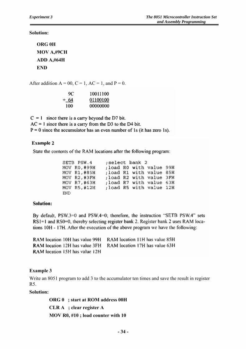
Example 1
Write a computer program to add the values 9CH and 64H and put the result in register A. Show the status of the carry flag (C) , auxiliary carry flag (AC), and the parity flag (P) after program execution.
- 33 -
The 8051 Microcontroller Instruction Set and Assembly Programming
Experiment 3
Solution:
ORG 0H MOV A,#9CH ADD A,#64H END
After addition A = 00, C = 1, AC = 1, and P = 0.
Example 3 Write an 8051 program to add 3 to the accumulator ten times and save the result in register R5. Solution: ORG 0 ; start at ROM address 00H CLR A ; clear register A MOV R0, #10 ; load counter with 10
- 34 -
The 8051 Microcontroller Instruction Set and Assembly Programming
Experiment 3
AGAIN: ADD A, #3 ; add 3 to contents of register A DJNZ R0, AGAIN ; decrease counter and repeat MOV R5, A ; save result in register R5 END Note: The maximum number of loops that can be achieved for the counter is 255 (FFH) since
the maximum value hold by an 8-bit register is FFH. Example 4 Write a program to (a) load the accumulator with the value 55H, and (b) complement the accumulator 500 times. Solution: Since 500 is larger than 255 (the maximum capacity of any register), we use two registers to hold the count. The following code shows how to use R2 and R3 for the count. ORG 00H MOV A, #55H MOV R3, #5 START: MOV R2, #100 AGAIN: CPL A DJNZ R2, AGAIN DJNZ R3, START END Example 5 Write an assembly program to send the value 55H to port 1 (P1) of the 8051 microcontroller continuously. Solution: ORG 0 MOV A, #55H BACK: MOV P1, A SJMP BACK END Example 6 Write an 8051 program to copy the value AAH into RAM memory locations 40H to 45H.
- 35 -

The 8051 Microcontroller Instruction Set and Assembly Programming
Experiment 3
Solution: ORG 0 ; Start with program code address 00H MOV A, #0AAH ; Load accumulator with AAH MOV R0, #40H ; Load pointer with address of first memory location MOV R2,#5 ; Load counter with 5 AGAIN: MOV @R0, A ; Copy 0AAH to RAM location pointed by R0 INC R0 ; Increment Pointer DJNZ R2, AGAIN ; Loop until counter = 0 END Example 7 Assuming that ROM space starting at 500H contains “IRAQ”, write an 8051 program to transfer the bytes into RAM locations starting at 40H. Use the indexed addressing mode. Solution: ORG 0000 MOV DPTR, #MSG ; Load ROM pointer MOV R0, #40H ; Load RAM pointer MOV R2, #4 ; Load counter with the number of characters BACK: CLR A ; A = 0 MOVC A, @A+DPTR ; Move data from ROM to accumulator MOV @R0, A ; Save it in RAM INC DPTR ; Increment ROM pointer INC R0 ; Increment RAM pointer DJNZ R2, BACK ; Loop until counter = 0 HERE: SJMP HERE ; ---------- On-chip code space used for storing data ORG 500H MSG: DB ‘IRAQ’ END 7. Procedure
Implement the examples presented above and verify their results with the aid of the MCU 8051 MCU IDE emulator.
- 36 -

The 8051 Microcontroller Instruction Set and Assembly Programming
Experiment 3
8. Exercises
Exercise 1: Write an 8051 assembly program to put the value 8DH in RAM locations 30H to 34H.
Exercise 2: Write an assembly program to copy the internal code byte at address 300H to external RAM address 300H.
Exercise 3: Write an 8051 assembly program to continuously send out to port 1 the alternating values 55H and AAH. Make a certain time delay between the two successive values. Note that the value AAH is the binary complement of the value 55H.
Exercise 4: Use the ASEM 51 assembler to generate the HEX file for the following 8051 program:
MOV A, #0 MOV R1, A ADD A, #79H JNC TARGET1 INC R1 TARGET1: ADD A, #0F5H JNC TARGET2 INC R1 TARGET2: ADD A, #0E2H JNC OVER INC R1 OVER: MOV R0, A END
9. Discussion
1. What is the result of the following code and where is it kept?
MOV R4, #25H MOV A, #1FH ADD A, R4
2. Write a simple 8051 program in which the value 55H is added 5 times. 3. What is the value of the C flag after the following code?
CLR C CPL C
- 37 -

The 8051 Microcontroller Instruction Set and Assembly Programming
Experiment 3
4. Find the number of times the following loop is performed:
MOV R6, #200 BACK: MOV R5, #100 HERE: DJNJ R5, HERE DJNZ R6, BACK
5. What is the difference between the SJMP and LJMP instructions? 6. Write a program to set the LSB and MSB of port1 and reset all other bits of the port
continuously. 7. Write an 8051 program to exchange the contents of the stack pointer SP and the flag
register PSW. 8. Write a simple program to copy the content of internal RAM locations 08H-0FH to RAM
locations 30H-37H. 9. Write a program to copy the contents of code ROM addresses 0100H-0102H to internal
RAM locations 20H-22H. 10. What is the content of the list file produced by the assembler?
- 38 -

The 8051 Microcontroller Trainer Experiment 4
Experiment 4
The 8051 Microcontroller Trainer Objectives The purpose of this experiment is to demonstrate the construction and operation of the MCT-8051 Microcontroller Trainer Board in developing practical 8051-based projects, and to understand the principles of transferring 8-bit data via output ports of the 8051 trainer. 1. Introduction The MCT-8051 microcontroller trainer is developed solely for learning purposes. Using this trainer, the user can write 8051 assembly language code, test the code, run the code, and see the project working. Figure 1 presents a picture for this trainer.
Figure 1: The MCT-8051 Microcontroller Trainer
The microcontroller trainer consists of:
• 87C52 Microcontroller chip clocked at 22.1184 MHz. • 7 I/O ports with 56 lines. • SRAM with 24 KB available as user program memory. • Flash ROM with available 30 KB as non-volatile program storage and data logging. • 2 Serial ports for connection with the PC. • DC Power Supply with 4-output voltages (+5V, -5V, +12V, -12V). • Built-in 8-bit LED data display module. • Built-in 8-bit switch input module. • Built-in 7-segment display module. • Monitor program burned into the on-chip ROM of the 87C52 microcontroller for easy
code development.
- 39 -

The 8051 Microcontroller Trainer Experiment 4
The user can load his programs into the MCT-8051 trainer using the Windows HyperTerminal Emulator. The necessary requirements for running the MCT-8051 trainer are:
• AC Voltage Source of 240V, and 50Hz. • Computer equipped with a serial port. • Standard 9-pin serial cable. • Microsoft Windows XP operating system. • Assembler such as the ASEM51 or the MIDE-51. • Text Editor Program such as Notepad or MS Edit. • Terminal Emulation Program such as the Windows XP HyperTerminal Program.
2. Schematic Diagram for the MCT-8051 Trainer Board The trainer uses the Philips 87C52 microcontroller chip with additional supporting circuitry for external RAM (62256), external ROM (39F512), external ports using the 8255 programmable I/O chip, and an RS232 Driver IC (MAX232) for serial port interfacing. Figure 2 shows the overall schematic diagram of the trainer. As shown from this figure, the address lines of the 87C52 microcontroller (Port 0 and Port 2) are connected to the address lines of the Flash ROM (39F512) and the external SRAM (62256) via the 74373 D-latch buffer. This is necessary for Address/Data multiplexing. The same principle is utilized for connecting the 87C52 microcontroller with two 8255 peripheral programmable chips. These two chips are used together to form 6 external I/O ports in addition to P1. The technique used to address the I/O ports is the memory mapped I/O method, with the use of decoding circuitry to locate the addresses of the I/O ports.
Most of the chips are designed to connect directly to the bus, so all that's needed is to connect their address pins to the lower pins of the address bus, their data pins to the data bus, and their write and output enable pins to the WR and RD/PSEN signals. All the chips see all those signals, but only the chip that gets a low signal on its chip select pin will communicate with the processor. All the other chips remain silent. The 8752 microcontroller provides the address information before it signals RD, WR or PSEN to cause the chip to communicate, and the logic gates are chosen so that the chip select signals are generated before the 8752 sends the control signals.
- 40 -

The 8051 Microcontroller Trainer Experiment 4
Figure 2: The Schematic Diagram of the MCT-8051 Trainer 3. The Address Decoding Logic Circuitry and Memory Map The basic idea behind the address decoding is that some logic chips are connected to the upper address bits of the system bus and are activated from the chip select signals, depending on what memory range the processor is accessing.
The A15 signal goes directly to the RAM, so the RAM gets selected for all addresses where A15 is low (0000 to 7FFF). A11 to A14 go to a 4-input NAND gate. That gate outputs low when all four signals are high, and its output is low in all other cases. That gate and the A15 signal go to the other 4-input NAND gate and to the 74HC138 chip. When A15 is high, and any of A11 to A14 are low, the other 4-input NAND gate drives the Flash ROM chip select low. That means the Flash ROM is enabled from the range 8000 to F7FF. Those same two signals also go to the 74HC138 chip's G1 and G2a inputs. The 74HC138 address decoder only drives one of its outputs low when G1 is high and when G2a is low. That means the 74HC138 chip drives one of its 8 signals in the range of F800 to FFFF. The three address inputs to the
- 41 -

The 8051 Microcontroller Trainer Experiment 4
74HC138 are connected to A8, A9 and A10, so that each of those signals corresponds to a 256 byte range. If you follow where each one goes, you'll see they correspond to the memory map for the peripherals.
Based on this concept, the memory map of the MCT-8051 trainer system is depicted in Fig.3. The address space from 0000H to 1FFFH is reserved for the built-in software which is burned inside the on-chip EPROM of the microcontroller. This software is used for system booting and user program monitoring and running. Thus, the user program should be loaded at the external RAM with starting address of 2000H. The external RAM actually represents the program (code) memory. An additional Flash ROM is also provided to the user for permanent program and data storage with an address space between 8000H and F7FFH. The external ports can be accessed from their addresses with an allocated address space from F800H to FEFFH. The remaining address space is left unused.
Figure 3: The Memory Map of the Trainer System
- 42 -
The 8051 Microcontroller Trainer Experiment 4
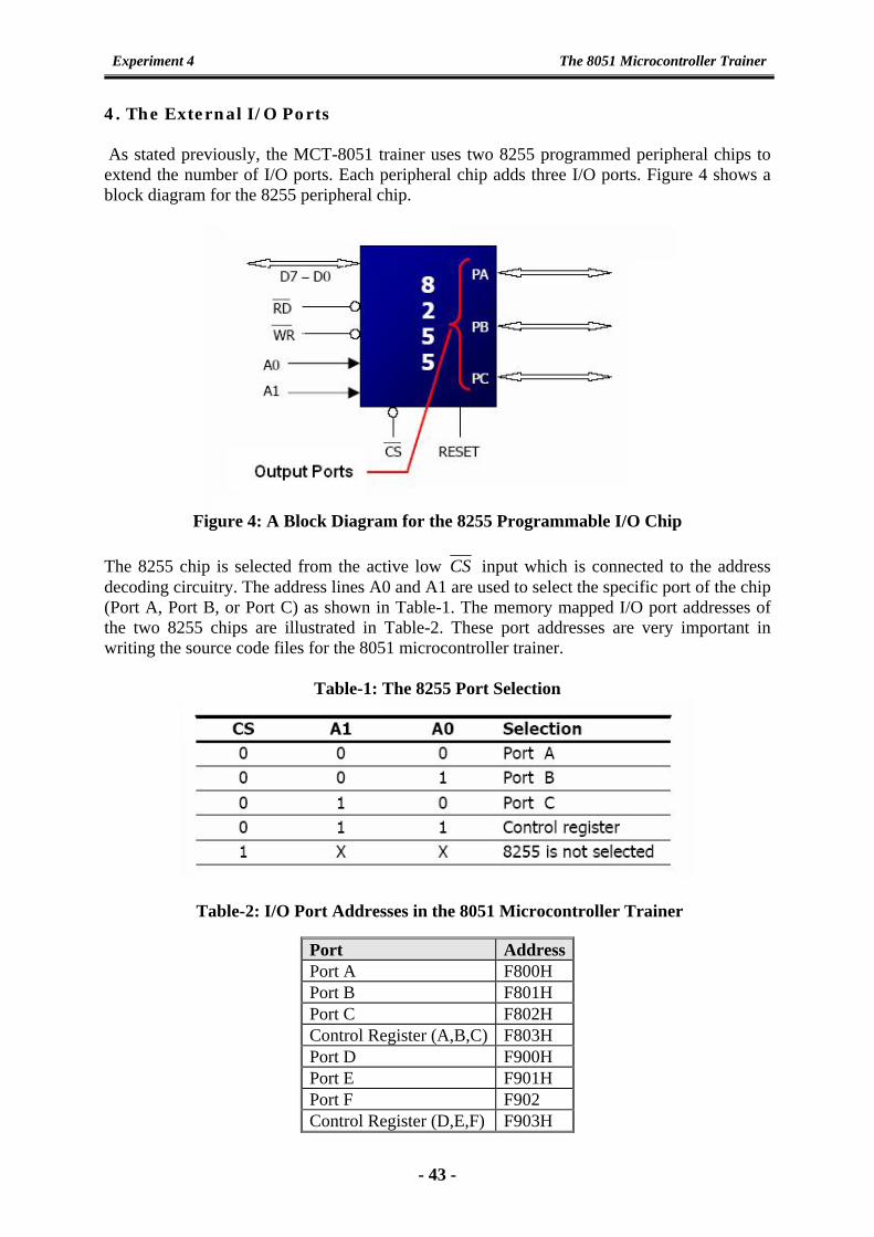
4. The External I/O Ports As stated previously, the MCT-8051 trainer uses two 8255 programmed peripheral chips to extend the number of I/O ports. Each peripheral chip adds three I/O ports. Figure 4 shows a block diagram for the 8255 peripheral chip.
Figure 4: A Block Diagram for the 8255 Programmable I/O Chip
The 8255 chip is selected from the active low CS input which is connected to the address decoding circuitry. The address lines A0 and A1 are used to select the specific port of the chip (Port A, Port B, or Port C) as shown in Table-1. The memory mapped I/O port addresses of the two 8255 chips are illustrated in Table-2. These port addresses are very important in writing the source code files for the 8051 microcontroller trainer.
Table-1: The 8255 Port Selection
Table-2: I/O Port Addresses in the 8051 Microcontroller Trainer
Port AddressPort A F800H Port B F801H Port C F802H Control Register (A,B,C) F803H Port D F900H Port E F901H Port F F902 Control Register (D,E,F) F903H
- 43 -

The 8051 Microcontroller Trainer Experiment 4
The control word stored in the control register depends on the mode of 8255 operation. The ports of the 8255 can be programmed in one of the following modes: 1. Mode 0 (Simple I/O)
In this mode, any of the ports A, B, CL, or CU can be programmed as input or output port, which means that all bits are input or all bits are output. There is no single-bit control as in ports (P0-P3) of the 8051 microcontroller. 2. Mode 1
In this mode of operation, ports A and B can be used as input or output ports with handshaking capabilities. Handshaking signals are provided by the bits of port C. 3. Mode 2
In this mode, port A can be used as a bidirectional I/O port with handshaking capabilities provided by port C. On the other hand, port B can either be used in mode 0 or mode 1.
4. BSR Mode (Bit Set/Reset Mode)
In this mode, only the individual bits of port C can be programmed. This mode is similar to the bitwise control of ports (P0-P3) of the 8051 microcontroller.
Figure 5 shows the construction of the control word for selecting one of the 8255 modes stated above. This control word should be sent to the control register of the 8255 programmable chip prior to selecting the specific port.
Figure 5: The 8255 Control Word Format for the I/O Mode
Based on Fig.5, the different conditions for the control word of the 8255 chip operating in the I/O mode can be generated as depicted in Table-3.
- 44 -

The 8051 Microcontroller Trainer Experiment 4
Table-3: Different Conditions for the Control Word in the 8255 Peripheral Chip
Port C Port CPort BPort AControl Byte
Bits 3:0 Bits 7:4Bits 7:0Bits 7:0Hex Decimal
Output OutputOutputOutput80H 128
Input OutputOutputOutput81H 129
Output Input OutputOutput88H 136
Input Input OutputOutput89H 137
Output OutputInput Output82H 130
Input OutputInput Output83H 131
Output Input Input Output8AH 138
Input Input Input Output8BH 139
Output OutputOutputInput 90H 144
Input OutputOutputInput 91H 145
Output Input OutputInput 98H 152
Input Input OutputInput 99H 153
Output OutputInput Input 92H 146
Input OutputInput Input 93H 147
Output Input Input Input 9AH 154
Input Input Input Input 9BH 155
5. Running the Terminal Emulation Program
As stated previously, the user object files (HEX files) can be loaded into the SRAM of the trainer via the HyperTerminal communication program of Windows XP. The assembly source file is first written with the aid of a text editor such as Notepad. This file is then applied to the assembler to check its syntax and to generate the object code file (HEX file). Finally, the HEX file is loaded into the 8051 trainer using the Windows HyperTerminal communication program. This process is depicted in Fig.6.
Figure 6: The Process of Loading the HEX file into the Trainer
- 45 -
The 8051 Microcontroller Trainer Experiment 4
First, the trainer should be connected to the serial port (COM1) of the PC via a suitable serial cable. The required steps for accessing the HyperTerminal program and establishing the communication process between the trainer and the PC are stated below:
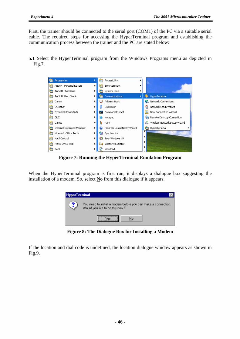
5.1 Select the HyperTerminal program from the Windows Programs menu as depicted in Fig.7.
Figure 7: Running the HyperTerminal Emulation Program
When the HyperTerminal program is first run, it displays a dialogue box suggesting the installation of a modem. So, select No from this dialogue if it appears.
Figure 8: The Dialogue Box for Installing a Modem
If the location and dial code is undefined, the location dialogue window appears as shown in Fig.9.
- 46 -

The 8051 Microcontroller Trainer Experiment 4
Figure 9: The Location Dialogue Box
5.2 Next, a connection name and icon should be provided as shown in Fig.10.
Figure 10: Selecting a Name and an Icon for the Connection
5.3 After providing the name, you will need to select the port where the 8051 trainer board is connected. In this case, COM1 is the proper choice.
- 47 -
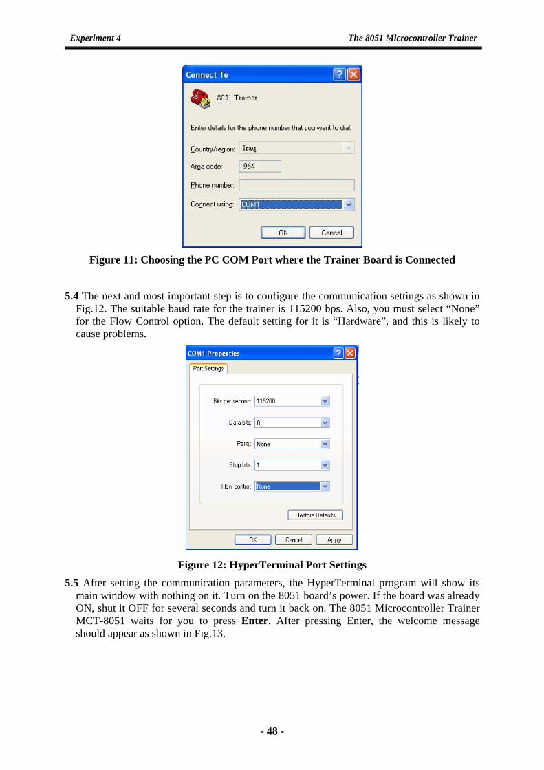
The 8051 Microcontroller Trainer Experiment 4
Figure 11: Choosing the PC COM Port where the Trainer Board is Connected
5.4 The next and most important step is to configure the communication settings as shown in Fig.12. The suitable baud rate for the trainer is 115200 bps. Also, you must select “None” for the Flow Control option. The default setting for it is “Hardware”, and this is likely to cause problems.
Figure 12: HyperTerminal Port Settings
5.5 After setting the communication parameters, the HyperTerminal program will show its main window with nothing on it. Turn on the 8051 board’s power. If the board was already ON, shut it OFF for several seconds and turn it back on. The 8051 Microcontroller Trainer MCT-8051 waits for you to press Enter. After pressing Enter, the welcome message should appear as shown in Fig.13.
- 48 -

The 8051 Microcontroller Trainer Experiment 4
Figure 13: The Welcome Message of the Built-in Monitor Program
5.6 To download the HEX file, select the command Send Text File from the Transfer menu as shown in Fig.14.
Figure 14: Downloading HEX Files
5.7 When the dialogue box for the file selection appears, you will need to change the file type to “All files (*,*)” before selecting the HEX object file as depicted in Fig.15.
Figure 15: Selecting the HEX File
- 49 -

The 8051 Microcontroller Trainer Experiment 4
After selecting the HEX file, the built-in monitor program of the trainer begins to download it. When the download process is completed successfully, the monitor program prints a summary of the download as shown in Fig.16. In order to run the downloaded HEX file, use the J (Jump) command followed by the starting address of the program to be executed which is usually 2000H.
Figure 16: HEX File Download
6. Procedure
In this experiment, we will use the 8051 trainer to test some 8051 assembly programs with the aid of the 8-bit LED module, and the input switch module which are built in the trainer itself and need no external circuitry for the interfacing process.
6.1 Connect Port A of the trainer to the 8-bit LED module as shown in Fig.17.
Figure 17: Connection Diagram between Port A of the Trainer and the 8-bit LED
Module
- 50 -

The 8051 Microcontroller Trainer Experiment 4
1. Use the MIDE-51 assembler or the MCU 8051 IDE Emulator to write and assemble the following source code file:
; Program to send a byte from Port A to the 8-bit LED module
ORG 2000H
PortA EQU 0F800H
PortReg EQU 0F803H
ESC EQU 003EH
MOV DPTR,#PortReg
MOV A,#80H ; All ports are output
MOVX @DPTR,A
Begin: MOV A,#55H
MOV DPTR,#PortA
MOVX @DPTR,A
LCALL ESC
JC EXIT
SJMP Begin
EXIT: MOV A,#00H
MOVX @DPTR,A
HERE: SJMP HERE
END
This program is used to send the value 55H to port A, which is connected directly to the 8-bit LED module. The program is stored at a starting RAM address of 2000H. The port addresses are first defined using the EQU pseudo instruction. The control word (80H) stored in the control register declares that all the 8255 ports are output ports. The required byte is transferred from the accumulator to Port A using the MOVX instruction after placing the port address at the data pointer (DPTR). This process is continuously repeated using the unconditional jump instruction (SJMP) unless the ESC key is pressed. The ESC key press is identified by means of a built-in subroutine stored at the on-chip EPROM of the microcontroller. Upon pressing the ESC key, the program exits from the loop and places the value 0 at Port A to turn off all the LEDs.
6.2 Download the object code file of the program into the RAM of the trainer and execute it using the command J and enter the address 2000 from the main window of the HyperTerminal emulation program. Note the blinking of the LEDs.
6.3 Use the MIDE-51 assembler or the MCU 8051 IDE Emulator to write and assemble the following source code file:
- 51 -

The 8051 Microcontroller Trainer Experiment 4
; Program to display a moving bit sequence
ORG 2000H
PortA EQU 0F800H
PortReg EQU 0F803H
ESC EQU 003EH
MOV DPTR,#PortReg
MOV A,#80H
MOVX @DPTR,A
MOV A,#01H
MOV DPTR,#PortA
Begin: MOVX @DPTR,A
RL A
LCALL ESC
JC EXIT
ACALL Delay
SJMP Begin
EXIT: MOV A,#00H
MOVX @DPTR,A
HERE: SJMP HERE
Delay: MOV R0,#0FFH
Loop1: MOV R1,#0FFH
Loop2: NOP
DJNZ R1,Loop2
DJNZ R0,Loop1
RET
END
This program is used to generate a moving bit sequence that moves continuously from right to left. This is done by first loading the accumulator with a single-bit sequence (01H) and rotating it continuously from right to left using the RL (Rotate Left) instruction. The content of register A is transferred continuously to Port A. A delay time is necessary between the consecutive sequences to make the movement visible. This is done by calling a delay subroutine consisting of two non-overlapping loops using registers R0 and R1. The instruction ACALL (Absolute Call) is used to reach subroutines within a maximum memory space of 2KB from the calling point in the main program. The LCALL (Long Call) instruction on the other hand can be used to call subroutines anywhere within the 64KB address space of the 8051. After finishing execution of the subroutine, the instruction RET (Return) transfers control back to the main program.
- 52 -

The 8051 Microcontroller Trainer Experiment 4
6.4 Download the object code file of the moving-bit program into the RAM of the trainer and execute it using the command J followed by the address 2000 from the main window of the HyperTerminal emulation program. Note the blinking of the LEDs in this case.
6.5 Connect the 8051 trainer as shown in Fig.18. This circuit is used to control the blinking of the LEDs wired to Port A from the switches wired to Port B.
Figure 18: Connection Diagram for Moving Input Data from Port A to Port B
6.6 Use the MIDE-51 assembler or the MCU 8051 IDE Emulator to write and assemble the following source code file: ; Program to get data from Port B and move it to Port A
ORG 2000H
PortA EQU 0F800H
PortB EQU 0F801H
PortReg EQU 0F803H
ESC EQU 003EH
MOV DPTR,#PortReg
MOV A,#82H ; Port B is input, Port A & C are output
MOV @DPTR,A
Begin: MOV DPTR,#PortB
- 53 -

The 8051 Microcontroller Trainer Experiment 4
MOVX A,@DPTR
MOV DPTR,#PortA
MOVX @DPTR,A
LCALL ESC
JC EXIT
SJMP Begin
EXIT: MOV A,#00H
MOV DPTR,#PortA
MOVX @DPTR,A
HERE: SJMP HERE
END
6.7 Download the object code file of the above program into the RAM of the trainer and execute it using the command J followed by the address 2000 from the main window of the HyperTerminal emulation program. Change the switches’ positions and note the LEDs when turning on and off.
6.8 Connect an oscilloscope to the trainer as shown in Fig.19. Put the oscilloscope’s probe of CH1 on pin P1.0 of Port 1.
Figure 19: An Oscilloscope Connected to Pin P1.0
6.9 Write and assemble the following assembly program, which is used to generate a pulse signal with 50% duty cycle. Download the object code file of the program into the trainer, and display the generated signal on the oscilloscope. Try to measure the frequency of the square wave in addition to its amplitude. Vary the delay time in the program by adjusting the values of R0 and R1 and measure the frequency of the signal each time.
- 54 -

The 8051 Microcontroller Trainer Experiment 4
ORG 2000H
ESC EQU 003EH
Again: SETB P1.0
ACALL Delay
CLR P1.0
ACALL Delay
LCALL ESC
JC EXIT
SJMP Again
EXIT: CLR P1.0
HERE: SJMP HERE
Delay: MOV R0,#1FH
Loop1: MOV R1,#1FH
Loop2: NOP
DJNZ R1,Loop2
DJNZ R0,Loop1
RET
END
7. Exercises
1. Write an assembly program to send the values 55H and AAH consequently into Port A of the trainer, and display them on the 8-bit LED module. Make a suitable delay between the two values.
2. Write an assembly program to generate a moving two-bit sequence from left to right and display it on the LEDs of the 8-bit module.
3. Write an assembly program to read input data from Port C of the trainer, complement them, and move them to Port B.
4. Write an 8051 assembly program to generate a pulse signal with a duty cycle of 25%. Display the generated signal on an oscilloscope and measure its frequency.
8. Discussion
1. A given memory chip has 12 address pins and 4 data pins. Find:
(a) The organization, and
(b) The capacity
2. Find the memory address space (Start Address and End Address) for the address decoding circuit presented in Figure 20 below.
- 55 -

The 8051 Microcontroller Trainer Experiment 4
Figure 20: A Memory Decoding Circuit
3. Find the data memory address space in the 8051 system shown in Figure 21 below.
Figure 21: An 8051 Microcontroller System
4. Find the control word of the 8255 peripheral chip for the following configurations:
(a) All the ports of A, B, and C are output ports (mode 0).
(b) PA = in, PB = out, PCL = out, and PCH = out.
5. For the 8051 system shown in Figure 22 below:
(a) Find the I/O port addresses assigned to ports A, B, C, and the control register.
(b) Find the control byte for PA = in, PB = out, PC = out.
(c) Write a program to get data from PA and send it to both ports B and C for this system.
- 56 -

The 8051 Microcontroller Trainer Experiment 4
Figure 22: The 8051 Microcontroller System for Q5
6. Write an 8051 program to read data from PA and test if it equals to 0 to send a HIGH signal to pin P1.0.
7. Write an 8051 program to implement a decade counter with its output connected to PB. Display the counter states on the 8-bit LED module with necessary delay between the consecutive states.
8. Write an 8051 assembly program to send the value 99H to ports B and C simultaneously.
- 57 -

The 8051 Microcontroller Trainer Experiment 4
This page is left intentionally blank
- 58 -

Interfacing the 8051 Microcontroller with 7-Segment LED Displays
Experiment 5
Experiment 5
Interfacing the 8051 Microcontroller with the 7-Segment LED Display
Objectives The purpose of this experiment is to learn driving 7-segment LED displays from the 8051 microcontroller trainer.
1. Theory
There are many applications of the light emitting diode (LED) in electronic circuits and systems. One of these applications is the Seven-Segment Display. It is composed of 8 LEDs, 7 segments are arranged as a rectangle for symbol displaying and there is an additional segment for decimal point displaying. The segments are marked with the letters from a to g, plus the dot or the decimal point, as shown in Fig.1. The purpose of this arrangement is to display any number by switching ON or OFF the particular LEDs. Figure 1 shows the pin configuration and picture of a typical 7 segment LED display.
Figure 1: Pin Configuration of the Seven Segment LED Display
There are basically two types of seven-segment display devices: common cathode (CC) and common anode (CA). In a common cathode display, all the seven legs (‘a’ through ‘g’) are of anode type and the common cathode will be connected to the ground. By energizing any of the legs with +5V, then this will switch the corresponding segment ON. In a common anode display on the other hand, all the seven legs are of cathode type and the common anode is connected to the power supply (+VCC) via a current-limiting resistor. In this case, each segment is energized by applying a logic 0 (GND) to it.
- 59 -

Interfacing the 8051 Microcontroller with 7-Segment LED Displays
Experiment 5
There are two methods for interfacing the seven-segment LED displays with the microcontroller:
1- Direct connection to the port pins of the 8051 microcontroller.
2- Using the 7447 and 7448 decoders.
In the first method, a look-up table is used to send the appropriate binary pattern for energizing the relevant LED segments in order to display the required number. Figure 2 depicts a block diagram for connecting a common-anode seven segment display directly with the microcontroller. Note that the common-anode display requires Active-Low inputs from the port of the microcontroller.
Figure 2: Connecting a CA Seven-Segment LED Display directly to the Microcontroller In the second method four of the port pins of the microcontroller are connected to the decoder inputs, which is in turn connected to the seven-segment LED display. In this case, the decoder takes the Binary Coded Decimal (BCD) as the input and outputs the relevant 7 segment code. Figure 3 shows the circuit diagram of connecting a common anode seven segment display to the 8051 microcontroller via the 7447 decoder.
Figure 3: Circuit Diagram for Interfacing a Common Anode Seven-Segment Display
using the 7447 Decoder
- 60 -

Interfacing the 8051 Microcontroller with 7-Segment LED Displays
Experiment 5
On the other hand, Figure 4 presents the circuit diagram for interfacing a common-cathode display with the 8051 microcontroller using the 7448 decoder.
Figure 4: Circuit Diagram for Interfacing a Common Cathode Seven-Segment Display
using the 7448 Decoder
The common digit drive patterns (0 to 9) of a common-cathode seven segment display are shown in Table-1 below.
Table-1: The Look-up Table for the Common-Cathode 7-Segment LED Display
Digit a b c d e f g0 1 1 1 1 1 1 0 1 0 1 1 0 0 0 0 2 1 1 0 1 1 0 1 3 1 1 1 1 0 0 1 4 0 1 1 0 0 1 1 5 1 0 1 1 0 1 1 6 1 0 1 1 1 1 1 7 1 1 1 0 0 0 0 8 1 1 1 1 1 1 1 9 1 1 1 1 0 1 1
In the 8051 microcontroller trainer kit, there is a module consisting of two seven-segment LED displays connected to the microcontroller via a single 7447 decoder. The user can select either one of the displays or both of them through two control inputs M6 and M7 as shown in Fig.5. The decoder inputs (M0, M1, M2, and M3) should be wired to one of the microcontroller ports. Table-2 illustrates the selection code of the two seven-segment displays.
- 61 -

Interfacing the 8051 Microcontroller with 7-Segment LED Displays
Experiment 5
Figure 5: The Seven-Segment Display Module of the Trainer
Table-2: Selection Sequence for the Seven Segment Displays of the Trainer
M7 M6 DIS2 DIS1
0 0 OFF OFF
0 1 OFF ON
1 0 ON OFF
1 1 ON ON
2. Procedure
2.1 Connect port A of the 8051 microcontroller trainer to the 7-segment display, and switch S0 and S1 as shown in Fig.6 below.
Figure 6: Test Setup used to drive the 7-Segment Displays from Port A
- 62 -
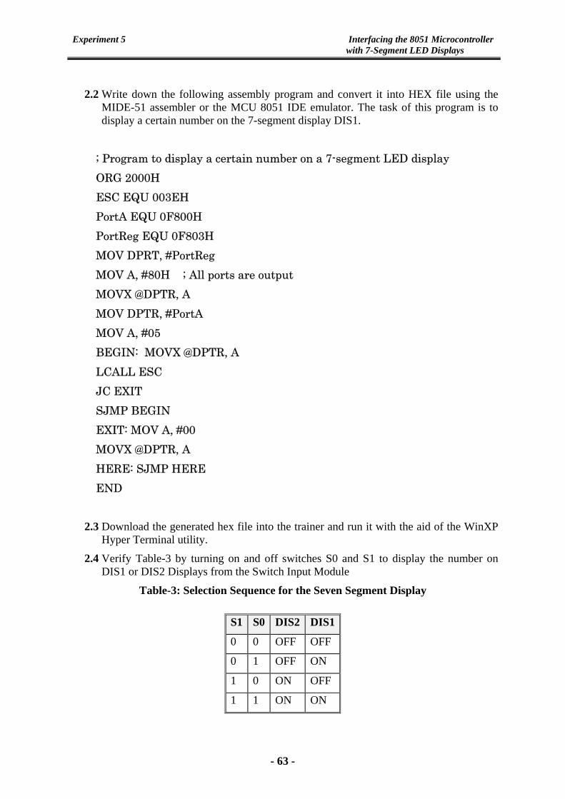
Interfacing the 8051 Microcontroller with 7-Segment LED Displays
Experiment 5
2.2 Write down the following assembly program and convert it into HEX file using the MIDE-51 assembler or the MCU 8051 IDE emulator. The task of this program is to display a certain number on the 7-segment display DIS1.
; Program to display a certain number on a 7-segment LED display ORG 2000H ESC EQU 003EH PortA EQU 0F800H PortReg EQU 0F803H MOV DPRT, #PortReg MOV A, #80H ; All ports are output MOVX @DPTR, A MOV DPTR, #PortA MOV A, #05 BEGIN: MOVX @DPTR, A LCALL ESC JC EXIT SJMP BEGIN EXIT: MOV A, #00 MOVX @DPTR, A HERE: SJMP HERE END
2.3 Download the generated hex file into the trainer and run it with the aid of the WinXP Hyper Terminal utility.
2.4 Verify Table-3 by turning on and off switches S0 and S1 to display the number on DIS1 or DIS2 Displays from the Switch Input Module
Table-3: Selection Sequence for the Seven Segment Display
S1 S0 DIS2 DIS1
0 0 OFF OFF
0 1 OFF ON
1 0 ON OFF
1 1 ON ON
- 63 -

Interfacing the 8051 Microcontroller with 7-Segment LED Displays
Experiment 5
2.5 Set switch S0 ON and switch S1 OFF and write and assemble the following program.
It is used to simulate a count-up BCD counter that counts from 0 to 9 repeatedly and displays the digits on DIS1. The delay time between each two successive numbers can be set from the delay subroutine.
; Program to simulate a decade up counter ORG 2000H ESC EQU 003EH PortA EQU 0F800H PortReg EQU 0F803H MOV DPRT, #PortReg MOV A, #80H ; All ports are output MOVX @DPTR, A MOV DPTR, #PortA START: MOV A, #00 ; Set initial value MOV R0, #10 ; Set loop counter to 10 AGAIN: MOVX @DPTR, A LCALL ESC JC EXIT ACALL DELAY INC A DJNZ R0, AGAIN SJMP START EXIT: MOV A, #00 MOVX @DPTR, A HERE: SJMP HERE DELAY: MOV R1, #04 L1: MOV R2, #0FFH L2: MOV R3, #0FFH L3: NOP DJNZ R3, L3 DJNZ R2, L2 DJNZ R1, L1 RET END
- 64 -
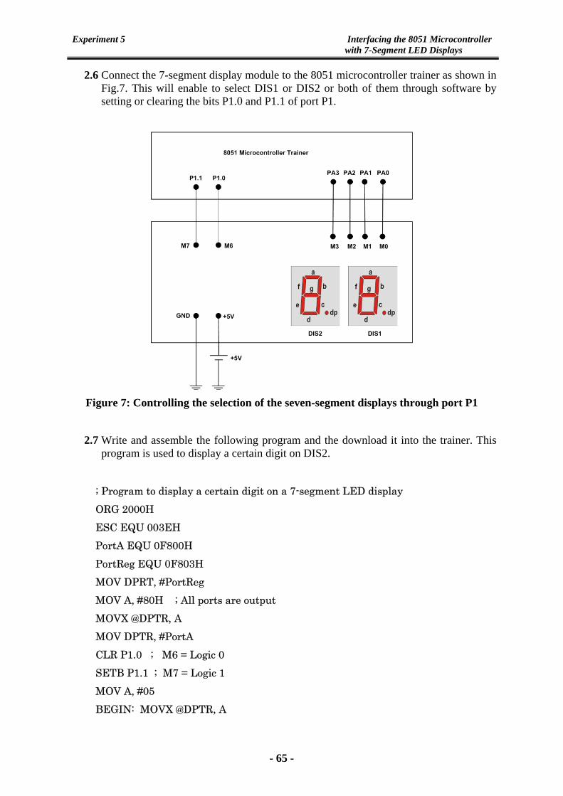
Interfacing the 8051 Microcontroller with 7-Segment LED Displays
Experiment 5
2.6 Connect the 7-segment display module to the 8051 microcontroller trainer as shown in
Fig.7. This will enable to select DIS1 or DIS2 or both of them through software by setting or clearing the bits P1.0 and P1.1 of port P1.
Figure 7: Controlling the selection of the seven-segment displays through port P1
2.7 Write and assemble the following program and the download it into the trainer. This
program is used to display a certain digit on DIS2.
; Program to display a certain digit on a 7-segment LED display ORG 2000H ESC EQU 003EH PortA EQU 0F800H PortReg EQU 0F803H MOV DPRT, #PortReg MOV A, #80H ; All ports are output MOVX @DPTR, A MOV DPTR, #PortA CLR P1.0 ; M6 = Logic 0 SETB P1.1 ; M7 = Logic 1 MOV A, #05 BEGIN: MOVX @DPTR, A
- 65 -

Interfacing the 8051 Microcontroller with 7-Segment LED Displays
Experiment 5
LCALL ESC JC EXIT SJMP BEGIN EXIT: MOV A, #00 MOVX @DPTR, A HERE: SJMP HERE END
2.8 Modify the previous program in order to display the value 55 on the seven segment displays and run it.
3. Exercises
1. Implement an assembly program that simulates a counter that counts as (00, 11, 22, 33, 44, 55, 66, 77, 88, 99) and repeats. Download and run this program using the WinXP Hyper-Terminal program.
2. Write and run an assembly program to simulate a count-down decade counter that counts down from 9 to 0 and repeats. Display the digits on DIS2.
4. Discussion
1. Write a look-up table for generating the 10 decimal digits in a common anode seven-
segment LED display.
2. Sketch a block diagram for connecting two common cathode seven segment LED displays to port P1 of the 8051 microcontroller via 7448 decoders. Consult the datasheet of the 74LS48 decoder from the internet to connect it properly in the circuit.
3. Sketch the necessary circuit diagram for controlling the 7-segment displays of the 8051 trainer manually through switches S0 and S1 of the input module. Write a computer program to display the two values 0 and 1 consecutively on DIS1.
4. Write an assembly program to simulate a count-up counter that counts up from 0 to 9 on displays DIS1 and DIS2 alternatively.
5. What is the main difference between common anode and common cathode seven-segment displays. Support your answer with the necessary diagrams.
- 66 -

Experiment 6 Stepper Motor Control Using the 8051 Microcontroller
Experiment 6
Stepper Motor Control Using the 8051 Microcontroller
Objectives The purpose of this experiment is to demonstrate the process of controlling a unipolar stepper motor via the 8051 microcontroller trainer kit to vary its direction of rotation, speed, and position. 1. Introduction to Stepper Motors Before launching into the practical procedure for interfacing the stepper motor with the 8051 microcontroller kit, it is necessary to understand the construction, types, and theory of operation of stepper motors. This section provides a brief introduction. 1.1 General Overview of Stepper Motors The stepper motor is a widely used device that translates electrical pulses into mechanical movement by producing a rotational torque. It is usually used in disk drives, dot-matrix printers, and robotics for position control. Figure 1 shows a typical stepper motor.
Figure 1: A Typical Stepper Motor
The most important features of stepper motors are:
1. High rotational accuracy
2. High torque
3. Small size
4. Wide speeds range
5. Accuracy in position control
- 67 -

Experiment 6 Stepper Motor Control Using the 8051 Microcontroller
1.2 Construction of Stepper Motors Stepper Motors commonly have a permanent magnet rotor (shaft) surrounded by a stator as shown in Figure 2.
Figure 2: Construction of the Stepper Motor
The rotor is constructed as a rotational shaft containing a permanent magnet and teeth as shown in Figure 3. The number of rotor teeth is inversely proportional to the step angle of rotation.
Figure 3: The Rotor of the Stepper Motor
The stator, on the other hand, contains the field winding of the motor as depicted in Figure 4. The most common stepper motors have four stator windings that are paired with a center-tapped common lead.
Figure 4: The Stator of the Stepper Motor
- 68 -
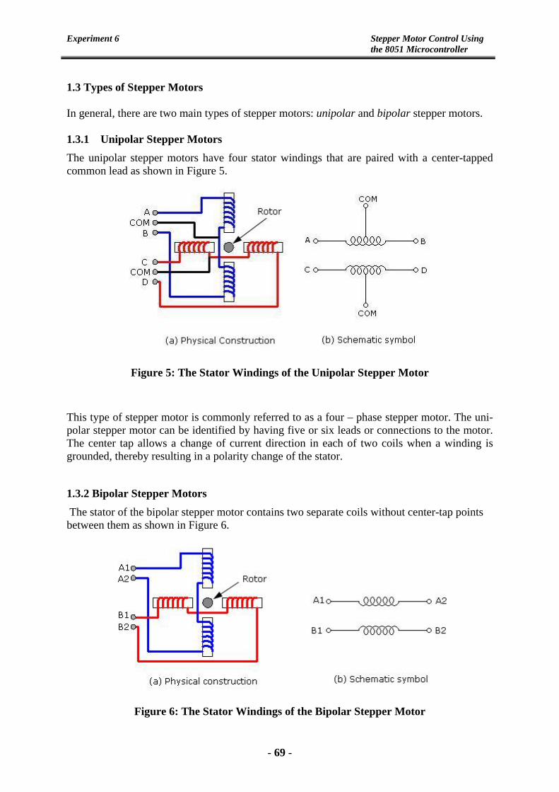
Experiment 6 Stepper Motor Control Using the 8051 Microcontroller
1.3 Types of Stepper Motors In general, there are two main types of stepper motors: unipolar and bipolar stepper motors. 1.3.1 Unipolar Stepper Motors The unipolar stepper motors have four stator windings that are paired with a center-tapped common lead as shown in Figure 5.
Figure 5: The Stator Windings of the Unipolar Stepper Motor
This type of stepper motor is commonly referred to as a four – phase stepper motor. The uni-polar stepper motor can be identified by having five or six leads or connections to the motor. The center tap allows a change of current direction in each of two coils when a winding is grounded, thereby resulting in a polarity change of the stator.
1.3.2 Bipolar Stepper Motors
The stator of the bipolar stepper motor contains two separate coils without center-tap points between them as shown in Figure 6.
Figure 6: The Stator Windings of the Bipolar Stepper Motor
- 69 -

Experiment 6 Stepper Motor Control Using the 8051 Microcontroller
The current in the stator windings can flow with two directions (two polarities). These types of stepper motors can be identified by having 4 leads. Although the unipolar stepper motor has a high torque, the control process of it is more difficult than that of the unipolar stepper motor and needs a special bridge circuit to make the current reverses its direction through the motor windings.
1.4 Stepper Motor Basic Theory of Operation Figure 7 shows a simplified internal construction for the stepper motor, where the rotor is made as a permanent magnet with a number of teeth and the stator is having four field windings. The stator windings are excited with a digital sequence for proper operation.
Figure 7: The Internal Construction of the Stepper Motor
While a conventional motor shaft runs freely, the stepper motor shaft moves in a fixed repeatable increment, which allows one to move it to a precise position. This repeatable fixed movement is possible as a result of basic magnetic theory were poles of the same polarity repel and opposite polarity attract. The direction of rotation is dictated by the stator poles. The stator poles are determined by the current sent through the wire coils. As the direction of the current is changed, the polarity is also changed causing the reverse motion of the rotor.
In order to more illustrate the basic principle of operation for the stepper motor, consider Figure 8 in which motor coils are excited by a digital sequence using the single coil excitation method.
- 70 -

Experiment 6 Stepper Motor Control Using the 8051 Microcontroller
Figure 8: Single Coil Excitation Method for the Stepper Motor
When a voltage is applied to coil A, then the north pole of the stator will be attracted towards the south pole of stator coil A in step number 1. In step 2, coil B is being excited instead of coil A and hence the rotor will move clock-wise one step towards coil B with a step angle of 90o. This process is repeated for steps 3 and 4 when exciting coils C and D respectively causing the rotor to move with a step angle of 90o in each step and in the clock-wise direction. As a result, the motor will rotate with 4 steps in each revolution.
In order to rotate the motor in the reverse direction, the excitation sequence must be reversed by applying voltages to coils A, D, C and finally to B.
1.5 Stepping Sequences for the Unipolar Stepper Motors As stated previously, the unipolar stepper motor contains four coils, and when exciting these coils with a proper digital sequence the motor will run. There are three basic digital stepping sequences.
1.5.1 Single-Coil Excitation Sequence In this method of excitation, only one coil is provided by a voltage at each instance while other coils are de-energized as shown in Table-1. This is the simpler method of excitation and is usually used to obtain higher speeds. However, it generates a low starting torque. It must be noted that although we can start with any of the sequences in Table-1, once we start we must continue in the proper order. For example, if we start with step 3 (0010), we must continue in the sequence of steps 4, 1, 2, etc.
- 71 -

Experiment 6 Stepper Motor Control Using the 8051 Microcontroller
Table-1: The Digital Sequence for the Single-Coil Excitation Method
1.5.2 Two – Coil Excitation Method In this type of excitation, two coils are excited in each instance as depicted in Table-2. This method is used to obtain high starting torque.
Table-2: The Digital Sequence for the Two-Coil Excitation Method
1.5.3 Half – Step Digital Sequence The half-step digital sequence is simply the combination of the single coil and double-coil excitations explained above. It is also known as the 8- step switching sequence, and is used for finer stepping resolutions. For example, a motor with 2-degree step angle can be used as a 1-degree step angle if the half-step sequence is applied. Table-3 presents the excitation method for the half-step digital sequence.
Table-3: Half-Step Digital Sequence
Step No. Coil A Coil B Coil C Coil D1 1 0 0 0
2 0 1 0 0
3 0 0 1 0
4 0 0 0 1
Step No. Coil A Coil B Coil C Coil D1 1 0 0 1
2 1 1 0 0
3 0 1 1 0
4 0 0 1 1
Step No. Coil A Coil B Coil C Coil D1 1 0 0 1
2 1 0 0 0
3 1 1 0 0
4 0 1 0 0
5 0 1 1 0
6 0 0 1 0
7 0 0 1 1
8 0 0 0 1
- 72 -

Experiment 6 Stepper Motor Control Using the 8051 Microcontroller
1.6 The Step Angle The step angle is defined as the minimum degree of rotation associated with a single step. It depends on the internal construction of the motor, in particular the number of teeth on the rotor. Various motors have different step angles. Table 1-1 shows some typical step angles for various stepper motors.
Table -4: Typical Stepper Motor Step Angles
Step Angle Steps per Revolution
0.72 500
1.8 200
2.0 180
2.5 144
5.0 72
7.5 48
12 24
It can be shown that the total number of steps per revolution is related with the step angle according to:
AngleSteprevolutionperSteps
o360= (1)
In a unipolar stepper motor, the rotor will move by a single tooth pitch after completing four consecutive digital sequences. In other words, the number of steps per revolution can be estimated from:
teethrotorofNumbercoilsofNumberrevolutionperSteps ×= (2)
1.7 Stepper Motor Speed The stepper motor speed, measured in steps per second (steps/s), is a function of the switching rate. So, by changing the delay time between the successive applied sequences, we can achieve various rotation speeds.
The motor speed in steps per second is related with the revolutions per minute (r.p.m) according to
60sec revolutionperStepsrpmondpersteps ×
= (3)
- 73 -

Experiment 6 Stepper Motor Control Using the 8051 Microcontroller
1.8 Holding Torque With the motor shaft at standstill or zero (r.p.m) condition, the amount of torque, from an external source, required to break away the shaft from its holding position is known as the holding torque. The unit of torque is kg-cm.
2. Stepper Motor Driving Circuit The stepper motor driver is used to provide the stepper motor coils with the necessary digital signals from any port of the microcontroller trainer kit as illustrated in Figure 9.
Figure 9: A Simplified Block Diagram for Connecting the Stepper Motor with the 8051
Trainer Kit The practical stepper motor to be used in this experiment is a unipolar 4-phase motor with 5 coil leads. Its part number is 24BYJ48 and it operates from a 5V DC supply. The DC resistance of each stator coil is 35Ω, which can be measured between the common lead and any of the other 4-coil terminals. Thus, the DC current per coil can be estimated as 140 mA (5V/35Ω). The datasheet step angle of this stepper motor is 5.625o. However, this motor is provided with a gear box which reduces the step angle to 0.18o, and thereby achieves high rotational accuracy. Figure 10 shows a picture for this motor.
Figure 10: A Picture Showing the Stepper Motor used in this Experiment
- 74 -

Experiment 6 Stepper Motor Control Using the 8051 Microcontroller
The motor coil leads can be identified practically by means of an ohmmeter. The resistance between each coil lead and the common terminal equals half the resistance between any of the coil leads. The common terminal is connected to the power supply (+5V). The stepper motor driving circuit consists of a 3-state buffer IC (74LS244) and a driver (ULN2003) as shown in Figure 11. The buffer is connected to any of the ports of the microcontroller and is used to isolate the specific microcontroller port from the stepper motor circuit and thereby protecting it from any back induced e.m.f. In Figure 12, the logic diagram of the 74LS244 buffer is presented, while Table-5 shows the function table for it.
Figure 11: Schematic Diagram of the Stepper Motor Driving Circuit As shown from Figure 12, the 74244 IC contains two groups of buffers with each group consisting of 4 buffers. In the stepper motor driving circuit, only one group is used. The inputs of the buffers (1A1, 1A2, 1A3, and 1A4) are connected to four pins of the microcontroller desired port, while the buffer outputs (1Y1, 1Y2, 1Y3, and 1Y4) are connected to the driver IC (ULN2003). The buffers transfer the digital signals from the microcontroller port into the ULN2003 driver when the control input G1 is Low (Logic 0).
Figure 12: The Logic Diagram of the 47LS244 Three-State Buffer
- 75 -
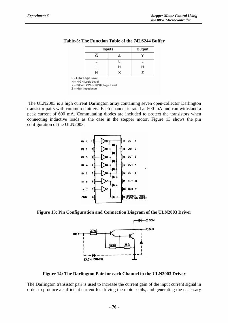
Experiment 6 Stepper Motor Control Using the 8051 Microcontroller
Table-5: The Function Table of the 74LS244 Buffer
The ULN2003 is a high current Darlington array containing seven open-collector Darlington transistor pairs with common emitters. Each channel is rated at 500 mA and can withstand a peak current of 600 mA. Commutating diodes are included to protect the transistors when connecting inductive loads as the case in the stepper motor. Figure 13 shows the pin configuration of the ULN2003.
Figure 13: Pin Configuration and Connection Diagram of the ULN2003 Driver
Figure 14: The Darlington Pair for each Channel in the ULN2003 Driver
The Darlington transistor pair is used to increase the current gain of the input current signal in order to produce a sufficient current for driving the motor coils, and generating the necessary
- 76 -

Experiment 6 Stepper Motor Control Using the 8051 Microcontroller
magnetic flux in each stator coil. When the input signal is High (Logic 1), the transistors saturate and the output voltage of the specific ULN2003 channel becomes Low (Logic 0), and therefore the current will passes from the common lead of the stepper motor through the stator coil and completes its path to ground through the saturating transistor of the driver. The maximum output current for each Darlington channel is about 500 mA which is adequate for the driving the coils of the stepper motor that need an approximate current of 140 mA as stated above.
The driving circuit is housed inside a plastic box. Figure 15 presents the stepper motor driver module to be connected with the microcontroller trainer kit.
Figure 15: The Stepper Motor Driver Module
3. Procedure
1- Connect the stepper motor driver module to the 8051 microcontroller kit by means of 2mm wires as shown in Figure 16.
Figure 16: Stepper Motor Module Connection with the 8051 Microcontroller Trainer
- 77 -

Experiment 6 Stepper Motor Control Using the 8051 Microcontroller
2- Use the MIDE-51 assembler or the MCU 8051 IDE simulator to write and assemble the program presented in Figure 17.
This program is used to run the stepper motor continuously in one direction. In this
program, the double coil excitation method is used to produce higher motor torque. So, this program produces the digital sequence shown in Table-2 repetitively. It can be noticed from Table-2 that once a certain digital sequence is generated, the remaining sequences can be obtained by continuous cyclic shift (Rotation) operation to each sequence. This can be done in software using the Rotate Right (RR) or Rotate Left (RL) assembly instructions. Figure 18 presents the flow chart for this program.
Figure 17: The Assembly Program used to run the Stepper Motor
Initially, the starting address of the program is set at 2000H so that it can be loaded at the external RAM (code memory in this case) of the microcontroller trainer system as stated in the previous experiments. The addresses of port-A and the control register for the 8255 peripheral I/O chip are then defined. A built-in subroutine for escaping is defined at an on-chip ROM address of 003EH. All microcontroller trainer ports are defined as output ports by sending the value 80H to the control register of the 8255 chip. After that, the address of port-A is loaded into the data pointer register (DPTR) which functions as a pointer to the external ports. The content of the accumulator is sent repeatedly into port-A after making the necessary cyclic shifting for the sequences, and a delay time is produced between the consecutive sequences. The Absolute call instruction (ACALL) calls subroutines with a target address within 2KB from the current program counter (PC), while the long call instruction (LCALL) calls subroutines with a maximum address space of 64KB. The user can stop the motor by pressing the ESC key, and a value of 0 is sent to port-A via the accumulator. The
- 78 -
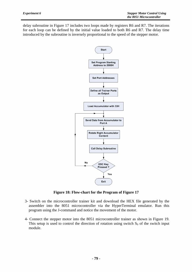
Experiment 6 Stepper Motor Control Using the 8051 Microcontroller
delay subroutine in Figure 17 includes two loops made by registers R6 and R7. The iterations for each loop can be defined by the initial value loaded to both R6 and R7. The delay time introduced by the subroutine is inversely proportional to the speed of the stepper motor.
Figure 18: Flow-chart for the Program of Figure 17
3- Switch on the microcontroller trainer kit and download the HEX file generated by the
assembler into the 8051 microcontroller via the HyperTerminal emulator. Run this program using the J-command and notice the movement of the motor.
4- Connect the stepper motor into the 8051 microcontroller trainer as shown in Figure 19.
This setup is used to control the direction of rotation using switch S0 of the switch input module.
- 79 -

Experiment 6 Stepper Motor Control Using the 8051 Microcontroller
Figure 19: Stepper Motor Connection Setup for Direction Control
5- Use the MIDE-51 assembler or the MCU 8051 IDE simulator to write and assemble the program presented in Figure 20.
The direction of rotation for the stepper motor can simply be reversed by reversing the cyclic shift of the sequences provided to the motor. For example, if the sequences presented in Table -2 are set in the clock-wise (CW) direction, the counter clock-wise (CCW) direction is obtained if the sequences are set in the order (1001, 0011, 0110, 1100) instead of the order (1001, 1100, 0110, 0011). This can be done by using the Rotate Left (RL) instruction instead of the Rotate Right instruction. The assembly program of Figure 20 is written to run the motor in two directions. The rotation direction is controlled by switch S0 of the switch input module which is connected to bit 0 of Port 1 (P1.0) of the trainer as depicted in Figure 19. Initially, the pin P1.0 is defined as an input pin by setting it to logic 1. Then, its value is tested according to the JB (Jump if bit) conditional instruction. If the value of P1.0 is 0 then clockwise direction is maintained by right rotating the content of the accumulator. Otherwise, the counter clockwise direction is achieved by left rotating the content of the accumulator. This condition is tested continuously before outputting the value in the accumulator to port A.
6- Switch on the microcontroller trainer kit and download the HEX file generated by the assembler into the 8051 microcontroller via the HyperTerminal emulator. Run this program using the J-command and notice the movement of the motor in either direction. Change the position of switch S0 to see the reversal of direction for the stepper motor.
- 80 -
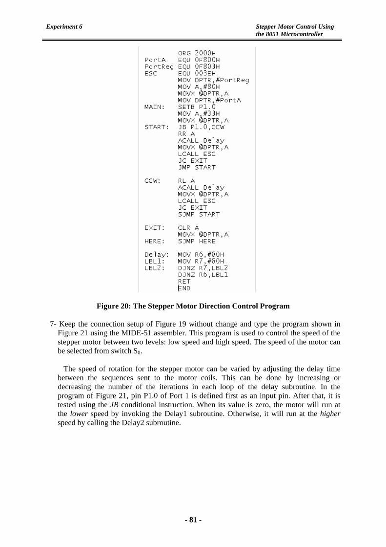
Experiment 6 Stepper Motor Control Using the 8051 Microcontroller
Figure 20: The Stepper Motor Direction Control Program
7- Keep the connection setup of Figure 19 without change and type the program shown in Figure 21 using the MIDE-51 assembler. This program is used to control the speed of the stepper motor between two levels: low speed and high speed. The speed of the motor can be selected from switch S0. The speed of rotation for the stepper motor can be varied by adjusting the delay time between the sequences sent to the motor coils. This can be done by increasing or decreasing the number of the iterations in each loop of the delay subroutine. In the program of Figure 21, pin P1.0 of Port 1 is defined first as an input pin. After that, it is tested using the JB conditional instruction. When its value is zero, the motor will run at the lower speed by invoking the Delay1 subroutine. Otherwise, it will run at the higher speed by calling the Delay2 subroutine.
- 81 -

Experiment 6 Stepper Motor Control Using the 8051 Microcontroller
Figure 21: The Stepper Motor Speed Control Program
8- Switch on the microcontroller trainer kit and download the HEX file generated by the assembler into the 8051 microcontroller via the HyperTerminal emulator. Run this program using the J-command and notice the rotation of the motor in either speed. Change the position of switch S0 to see the increase or decrease in the stepper motor’s speed.
9- Connect switch S1 to pin P1.1 in the microcontroller system as shown in Figure 22. This
setup will be used to control both the direction of rotation and the speed of the motor in the same time.
- 82 -

Experiment 6 Stepper Motor Control Using the 8051 Microcontroller
Figure 22: Stepper Motor Connection Setup for Direction and Speed Control
10- Use the MIDE-51 assembler to write and assemble the program presented in Figure 23. In this program switch S0 is responsible to the direction inversion, while switch S1 is used to increase or decrease the speed of the motor. Pins P1.0 and P1.1 of Port 1 are first defined as input pins. The value of bit P1.0 is then tested using the JB instruction to determine the direction of rotation. The program contains two main loops, each for a specific direction. The speed of the motor is determined by calling the appropriate delay subroutine depending on the value of bit P1.1. This condition is tested inside each of the two main loops of the program.
11- Switch on the microcontroller trainer kit and download the HEX file generated by the
assembler into the 8051 microcontroller via the HyperTerminal emulator. Run this program using the J-command and try to control the motor’s rotational direction and speed using switches S0 and S1 respectively.
- 83 -

Experiment 6 Stepper Motor Control Using the 8051 Microcontroller
Figure 23: The Assembly Program used for Direction and Speed Control
12- Reconnect the stepper motor system as depicted in Figure 16. This setup is used to
control the position of the stepper motor. The primary difference between stepper and conventional DC motors is the ease with which the position of the stepper motor is controlled accurately. This can be done be determining the angle of rotation for motor movement. The angle of motion for the stepper motor depends in turn on its step angle. It is well-known that the stepper motor moves one step per each step angle. So, the total number of steps required for a certain rotational angle is determined by dividing the angle of movement by the step angle as illustrated previously in equation 1.
- 84 -

Experiment 6 Stepper Motor Control Using the 8051 Microcontroller
For the stepper motor used in this experiment, the step angle is 0.18o. This means that in order to rotate the motor one complete revolution, the motor needs to move 2000 steps (360o/0.18o). Based on this concept, Table-6 presents the total number of steps required for some specific angles of rotation.
Table-6: Number of Steps for Some Specific Angles of the 24BYJ48 Stepper Motor
Angle of Movement Number of Steps45o 250 90o 500 135o 750 180o 1000 225o 1250 270o 1500 315o 1750 360o 2000
13- Use the MIDE-51 assembler to write and assemble the program presented in Figure 24.
This program is used to move the stepper motor clockwise with an angle of 180o. The program includes two loops, inner and outer. The inner loop contains the four necessary steps for the double-excitation sequences, while the outer loop repeats these sequences 250 times. Thus, the total number of the motor steps is 250×4 = 1000 steps as indicated in Table-6.
Figure 24: The Program used for the Stepper Motor’s Position Control of
- 85 -

Experiment 6 Stepper Motor Control Using the 8051 Microcontroller
4. Discussion 1- State the features of stepper motors over conventional DC motors. 2- Explain the differences between unipolar and bipolar stepper motors. 3- Suggest a driving circuit for the bipolar stepper motor. Try to search the internet for such
task. 4- Sketch a flow-chart for the stepper motor direction control program of Figure 20. 5- Write a computer program to rotate the stepper motor by one complete revolution in any
direction and stopping it. 6- Write an 8051 assembly program to rotate the stepper motor by 90o clockwise, and then
90o counter-clockwise. Use Table-6 to estimate the required steps. 7- Write an 8051 assembly program to rotate the stepper motor continuously using the half-
step sequence shown in Table-3. What would be the step angle in this case? 8- Modify the schematic diagram of Figure 11 to control two unipolar stepper motors in the
same time.
- 86 -

Experiment 7 Digital to Analog Converter Interfacing with the 8051 Microcontroller
Experiment 7
Digital to Analog Converter Interfacing with the 8051 Microcontroller
Objectives The purpose of this experiment is to learn connecting a digital to analog converter (DAC) module with the 8051 microcontroller unit, and writing assembly programs to generate different types of waveforms. 1. Introduction to Digital to Analog Converters A digital-to-analog converter, or simply DAC, is a semiconductor device that is used to convert a digital code into an analog signal. Digital-to-analog conversion is the primary means by which digital equipment such as computer-based systems are able to translate digital data into real-world signals that are more understandable to or useable by humans, such as music, speech, pictures, video, and the like. It also allows digital control of machines, equipment, household appliances, and the like. A typical digital-to-analog converter outputs an analog signal, which is usually voltage or current that is proportional to the value of the digital code provided to its inputs. Most DACs have several digital input pins to receive all the bits of its input digital code in parallel (at the same time). Some DACs, however, are designed to receive the input digital data in serial form (one bit at a time), so these only have a single digital input pin. Figure 1 presents a block diagram for an 8-bit DAC.
Figure 1: Block Diagram of an 8-bit Digital to Analog Converter
2. Types of Digital to Analog Converters There are in general two methods for converting digital code to analog signals: the binary weighted method and the R/2R ladder method. A simple binary weighted DAC may be implemented using an OP-AMP circuit connected as a summer as shown in Figure 2. The output voltage is the sum of its input voltages. Each of its inputs uses a resistor of different binary weight, such that if R0=R, then R1=R/2, R2=R/4, R3=R/8,.., RN-1=R/(2N-1). The output of a summer circuit with N bits is:
- 87 -

Experiment 7 Digital to Analog Converter Interfacing with the 8051 Microcontroller
Vo = -VR (Rf / R) (DN-12N-1 + DN-22N-2+.....+D020) (1) Where VR is the voltage to which the bit is connected when the digital input is '1'. A digital input is '0' if the bit is connected to 0V (ground). A 4-bit binary-weighted DAC circuit is shown in Figure 2.
Figure 2: Op-Amp Summer Circuit Used as a 4-bit Binary Weighted DAC Where R0 = 2R1 = 4 R2 = 8 R3
The major problem with this circuit is the wide range of resistor values needed to build a DAC with a high number of digital inputs. Putting thin-film resistors that come in a wide range of values (e.g., from a few kΩs to several MΩs) on a single semiconductor chip can be very difficult, especially if high accuracy and stability are required. A better-designed and more commonly-used circuit for digital-to-analog conversion is known as the R-2R ladder DAC, a 4-bit version of which is shown in Figure 3. It consists of a network of resistors with only two values, R and 2R. The input DN to bit N is '1' if it is connected to a voltage VR and '0' if it is grounded. Thevenin's Theorem may be applied to prove that the output Vo of an R-2R ladder DAC with N bits is: Vo = VR/2N (DN-12N-1 + DN-22N-2+...+D020) (2) Thus, the output of the R-2R ladder in Figure 2 is Vo = VR/24 (D323+D222+D121+D020), or Vo = VR (D3 / 2 + D2 / 4 + D1 / 8 + D0 / 16). In effect, contribution of each bit to the analog output is proportional to its binary weight.
Figure 3: A 4-bit R-2R Ladder DAC
- 88 -

Experiment 7 Digital to Analog Converter Interfacing with the 8051 Microcontroller
3. Common Parameters for DACs Some common parameters for performance measurement of digital to analog converters are illustrated below:
• Resolution: This is the number of bits that the DAC has. If a DAC has n bits, then its output analog signal span can be divided (or "resolved") into 2n states, each corresponding to its own digital input code. The higher the number of bits, the better is the resolution of a DAC.
• Voltage Reference Input Range: This indicates the minimum and maximum
voltages that may be used as the DAC's external reference voltage. Example of an Actual Spec: 0V min; Vdd max.
• Bipolar Zero Error or Mid-scale Error: This is the deviation of the actual analog
output of the DAC from the ideal output of 0V when the 2's complement input code representing half-scale (all zeros) is loaded into the input register.
• Differential Non-Linearity (DNL): This is the difference between the actual or
measured output change and the ideal output change for a digital input change of 1 LSB, i.e., for a transition between two adjacent codes. Examples of Actual Specs: +/- 1 LSB; +/- 0.001% FSR typ.
• Integral Non-Linearity (INL) or Relative Accuracy: This is the maximum
deviation of the output from the straight line between the zero and full-scale points, excluding the effects of zero and full-scale errors. Example of an Actual Spec: +/-1 LSB typ.; +/- 4 LSB's max.
• Analog Output Range or Full-Scale Range: This is the difference between the
maximum and minimum analog output values that the DAC is specified to provide. Example of Actual Spec: -3V to +3V, Bipolar Mode.
• Logic Input Voltage, VIH (Logic “1”): This is the minimum voltage that the digital
inputs of the DAC are guaranteed to recognize as Logic “1”. Example of an Actual Spec: 2.4 V min.
• Logic Input Voltage, VIL (Logic « 0 ») : This is the maximum voltage that the
digital inputs of the DAC are guaranteed to recognize as a Logic "0". Example of an Actual Spec: 0.8 V max.
• Input Leakage Current, IIL : This is maximum leakage current exhibited by a digital
input at logic "0". Example of an Actual Spec: 2 µA max. for VIL = 0.4 V.
• Settling Time: This is the time required by the outputs of a DAC to reach and remain within a specified error band about its final value. This is measured from the digital input transition. Examples of Actual Specs: 1.5 µsec typ. for a 6V step; 1.0 µsec typ. for a 1 LSB step.
- 89 -

Experiment 7 Digital to Analog Converter Interfacing with the 8051 Microcontroller
• Analog Positive Power Supply (+Vs): This is the voltage range that can be used for the analog positive supply of the DAC. Example of an Actual Spec: +4.75V min.; +5.0V typ.; +13.2V max.
• Analog Negative Power Supply (-Vs): This is the voltage range that can be used for
the analog negative supply of the DAC. Example of an Actual Spec: -13.2V min.; -5V typ.; -4.75V max.
• Logic Positive Power Supply (+VL): This is the voltage range that can be used for
the logic positive supply of the DAC. Example of an Actual Spec: +4.75V min.; +5.0V typ.; +13.2V max.
• Logic Negative Power Supply (-VL): This is the voltage range that can be used for
the logic negative supply of the DAC. Example of an Actual Spec: -13.2V min.; -5V typ.; -4.75V max.
• Gain Error or Full-Scale Error: This indicates how closely the analog output of a
DAC matches its ideal value at full scale and may be expressed in mV or as a % of the FSR. For many DAC's, the ideal maximum output voltage is Vref-1 LSB. Example of an Actual Spec: +/-1.22 mV.
• Signal-to-Noise Ratio (SNR): This is the ratio of the amplitude of the analog output
of the DAC when the output is set to full-scale to the amplitude of the output when it is set to zero. Example of an Actual Spec: 107 dB min.; 110 dB typ. for 20 Hz-30 kHz.
• Total Harmonic Distortion (THD): This is the ratio of the rms sum of the first few
(2nd to 6th) harmonic components of the DAC output to the DAC output's fundamental value, usually expressed in dB. Example of an Actual Spec: -80 dB typ.
4. The DAC0808 Digital to Analog Converter IC The DAC0808 is an 8-bit digital to analog converter IC which uses the R/2R ladder technique. Figure 4 presents the pin configuration diagram for this IC. In the DAC0808, the digital inputs are converted to current (Iout), and by connecting a resistor to the Iout pin, the output signal can be converted to voltage. The total current provided by the Iout pin is a function of the binary inputs ( D0 – D7) of the DAC0808 and the reference current (Iref), and is given as:
⎟⎠⎞
⎜⎝⎛ +++++++=
25612864321684201234567 DDDDDDDD
II refout (3)
where D0 is the LSB, D7 is the MSB for the inputs, and Iref is the input current that must be applied to pin 14.
- 90 -

Experiment 7 Digital to Analog Converter Interfacing with the 8051 Microcontroller
Figure 4: Pin Configuration of the DAC0808
The digital input pins in Figure 4 are labeled A1 through A8, but note that A1 is the Most Significant Bit, and A8 is the Least Significant Bit (the opposite of the normal convention). The output current from pin 4 ranges between 0 (when the inputs are all 0) to Iref × 255/256 when all the inputs are 1. Figure 5 shows a typical applied circuit for the DAC0808 by connecting it with the 8051 trainer kit.
Figure 5: Interfacing the DAC0808 with the 8051 Microcontroller Kit
- 91 -

Experiment 7 Digital to Analog Converter Interfacing with the 8051 Microcontroller
In the circuit of Figure 5, an OP-AMP is connected as a current to volt converter to the output pin (pin 4) of the DAC0808 to get an output voltage Vout. This voltage is related with the output current of the DAC0808 by:
foutout RIV .= (4) The reference current of the DAC0808 is given by:
1/ RVI CCref = (5) If R1 = R2 = 2.7kΩ and Rf = 2.2 kΩ, then Iref = 1.85 mA, and Vout (max) ≈ 4V. In this case, the full-scale output voltage VFS is approximately 4V. The output voltage resolution is VFS/(2n-1) = 4V/255 = 0.015686V. The required digital input code in decimal is thus:
015686.0255 out
FS
outin
VVV
D =×= (6)
5. Generating Sinusoidal Waves The 8051 microcontroller can be used to generate a sine wave when connecting it with a digital to analog converter. To generate the sine wave, it is first required to produce a table whose values represent the magnitude of the sine of angles between 0 and 360 degrees. The values for the sine function vary from -1.0 to +1.0 for 0 to 360 degree angles. Therefore, the table values are integer numbers representing the voltage magnitude for the sine of the angle. This method ensures that only integer numbers are output to the DAC by the 8051 microcontroller. For example, the sine wave shown in Figure 6 takes values from 0V to 3V and can be described by:
θsin5.15.1 ×+=outV (7)
Figure 6: A Sine Wave Varying from 0 to 3V
- 92 -

Experiment 7 Digital to Analog Converter Interfacing with the 8051 Microcontroller
To generate this sine wave, Table-1 is produced by assuming a full-scale voltage of 4V and applying equations (7) and (6) respectively with a step-angle of 15o.
Table-1: Angle versus Voltage Magnitude for the Generated Sine Wave
Angle θ Vout (V) Din (Decimal) 0 1.5 96 15 1.88 120 30 2.25 144 45 2.56 163 60 2.88 179 75 2.94 188 90 3 192 105 2.94 188 120 2.8 179 135 2.56 163 150 2.25 144 165 1.88 120 180 1.5 96 195 1.11 71 210 0.75 48 225 0.44 28 240 0.2 12 255 0.05 3 270 0 0 285 0.05 3 300 0.2 12 315 0.44 28 330 0.75 48 345 1.11 71 360 1.5 96
Similarly, one can generate different types of waveforms such as the square wave, ramp wave, triangular wave, stair-case wave …etc by producing the magnitude values and the required digital input sequence for each value.
- 93 -

Experiment 7 Digital to Analog Converter Interfacing with the 8051 Microcontroller
6. Procedure 6.1 Connect the DAC module with the input switch module as shown in Figure 7. Try to
measure the DC output voltage for each input digital sequence as shown in Table-2 with the aid of a digital multi-meter.
Figure 7: Measuring the Output Analog Voltage for each Input Digital Sequence
Table-2: Output Analog Voltage for Different Input Data
Input Sequence (HEX) Vout (V) 00 19 32 4B 64 7D 96 AF C8 E1 FF
- 94 -

Experiment 7 Digital to Analog Converter Interfacing with the 8051 Microcontroller
6.2 Connect the inputs of the DAC module to port 1 of the 8051 microcontroller kit, and its
output with an oscilloscope as shown in Figure 8 below.
Figure 8: Interfacing the DAC Module with the 8051 Microcontroller Trainer 6.3 Use the MIDE-51 assembler to write and assemble the following program for generating
a square wave. ; SQUARE WAVE GENERATION ORG 2000H ESC EQU 003EH AGAIN: MOV A,#0FFH MOV P1,A ACALL DELAY MOV A,#00 MOV P1,A ACALL DELAY LCALL ESC JC EXIT SJMP AGAIN EXIT: CLR A MOV P1,A HERE: SJMP HERE DELAY: MOV R0,#255 L1: DJNZ R0,L1 RET END
Figure 9: The Assembly Program used to generate a Square Wave
- 95 -

Experiment 7 Digital to Analog Converter Interfacing with the 8051 Microcontroller
This program sends the values FFH and 00H alternatively to Port 1. The delay time can be adjusted to vary the frequency of the generated signal. Download the hex file of this program into the 8051 microcontroller kit using the HyperTerminal utility. The square wave displayed on the oscilloscope should seem like that of Figure 10. Try to measure the amplitude and frequency of the generated wave.
Figure 10: The Generated Square Wave 6.4 Use the MIDE-51 assembler to write the program below for generating a ramp wave
similar to that of Figure 12.
; RAMP SIGNAL GENERATION ORG 2000H ESC EQU 003EH AGAIN: CLR A BACK: MOV P1,A INC A LCALL ESC JC EXIT CJNE A,#192,BACK SJMP AGAIN EXIT: CLR A MOV P1,A HERE: SJMP HERE END
Figure 11: An 8051 Assembly Program for Generating a Ramp Signal
- 96 -

Experiment 7 Digital to Analog Converter Interfacing with the 8051 Microcontroller
Figure 12: The Generated Ramp Wave
This program increases the content of the accumulator linearly, and sends its value to Port 1 continuously, until its value reaches to 192 (3V). The program then resets register A and repeats. Download the hex file of this program into the 8051 microcontroller trainer and run it. Measure the frequency of the displayed wave on the oscilloscope. 6.5 Use the MIDE-51 assembler to type and assemble the program presented in Figure 13 to
generate a stair-case signal like that of Figure 14. The voltage levels of the signal are saved in a look-up table at the code memory of the 8051 microcontroller system. A data pointer is used to reach these data via the indexed addressing mode.
; STAIR-CASE SIGNAL GENERATION ORG 2000H ESC EQU 003EH COUNT EQU 5 AGAIN: MOV DPTR,#TABLE MOV R0,#COUNT BACK: CLR A MOVC A,@A+DPTR MOV P1,A ACALL DELAY INC DPTR LCALL ESC JC EXIT DJNZ R0,BACK SJMP AGAIN EXIT: CLR A MOV P1,A HERE: SJMP HERE DELAY: MOV R1,#0FH H1: DJNZ R1,H1 RET ORG 2500H TABLE: DB 0,64,128,192,255 END
Figure 13: An 8051 Program Used to generate a Stair-Case Signal
Figure 14: A Stair-Case Signal
- 97 -

Experiment 7 Digital to Analog Converter Interfacing with the 8051 Microcontroller
Display the stair-case signal on the oscilloscope and measure its amplitude and frequency. 6.6 Use the MIDE-51 assembler to write and assemble the program presented in Figure 15 to
generate a sine wave like that of Figure 6. The voltage levels of the sine wave in Table-1 are saved in a look-up table at the code memory of the 8051 microcontroller system with a starting address of 2500H. The frequency of this signal can be adjusted by inserting time delays between successive values of the signal levels.
; SINE WAVE SIGNAL GENERATION ORG 2000H ESC EQU 003EH COUNT EQU 25 AGAIN: MOV DPTR,#TABLE MOV R0,#COUNT BACK: CLR A MOVC A,@A+DPTR MOV P1,A INC DPTR LCALL ESC JC EXIT DJNZ R0,BACK SJMP AGAIN EXIT: CLR A MOV P1,A HERE: SJMP HERE ORG 2500H TABLE: DB 96,120,144,163,179,188,192 DB 188,179,163,144,120,96,71 DB 48,28,12,3,0,3,12 DB 28,48,71,96 END
Figure 15: The 8051 Program Used to generate a Sine Wave
Download the hex file of this program into the 8051 microcontroller trainer and run it by means of the HyperTerminal emulator. Display the generated sine wave at the oscilloscope and measure the signal frequency and amplitude. 7. Discussion 1. State other types of digital to analog converters. 2. Design an 8-bit R/2R ladder network DAC, and derive the necessary equation for its
output voltage. Determine the value of the output voltage when the digital input is 00FFH.
3. Design a 4-bit binary-weighted DAC, and derive the necessary equation for its output
voltage.
- 98 -
Experiment 7 Digital to Analog Converter Interfacing with the 8051 Microcontroller
4. For the DAC0808 circuit of Figure 5, determine the reference current Iref, output current
Iout, and output voltage Vout if the input digital signal is set at 3C69H. Assume that R1 = R2 = 3.9 kΩ, and Rf = 3.3 kΩ. What is the full-scale output voltage in this case?
5. Modify the program listed in Figure 9 to generate a pulse signal with a duty-cycle of
20%. 6. Write an 8051 assembly program to produce a decreasing ramp signal like that presented
below.
7. Write an 8051 assembly program to generate a triangular wave as shown in the figure below.
8. Derive a look-up table for generating a sine wave with a peak-to-peak amplitude of 4V, using a step angle of 30o. Write the necessary assembly program for generating this signal.
- 99 -

Experiment 7 Digital to Analog Converter Interfacing with the 8051 Microcontroller
This page is left intentionally blank
- 100 -

Experiment 8 Analog to Digital Converter Interfacing with the 8051 Microcontroller
Experiment 8
Analog to Digital Converter Interfacing with the 8051 Microcontroller
Objectives The purpose of this experiment is to learn how to interface an analog to digital converter (ADC) module with the 8051 microcontroller unit, and develop the necessary assembly program to run it. 1. Introduction The analog to digital converter (ADC) is a device that provides an output that digitally represents the input voltage or current level. Computers use binary (discrete) values, but in the physical world everything is analog (continuous). Temperature, pressure, humidity, and velocity are a few examples of physical quantities that we deal with every day. A physical quantity is converted to electrical signals (voltage or current) using a device called a transducer. Transducers are also referred to as sensors. Sensors for temperature, velocity, pressure, light, and many other natural quantities produce an output voltage (or current). Therefore, we need an analog-to-digital converter to translate the analog signals to digital numbers so that the microcontroller can read and process them. The resolution of an ADC is the number of output bits it has. An ADC has n-bit resolution where n can be 8, 10, 12, 16 or even 24 bits. The higher-resolution ADC provides a smaller step size, where the step size is the smallest change that can be recognized by an ADC. Figure 1 shows a block diagram for an 8-bit parallel-out ADC.
Figure 1: An 8-bit ADC
An ADC has an analog reference voltage (Vref) or current against which the analog input is compared. The step size is equal to:
nrefV
SizeStep2
= (1)
- 101 -

Experiment 8 Analog to Digital Converter Interfacing with the 8051 Microcontroller
The step size thus is dependent on the reference voltage and the resolution of the ADC. Table-1 shows the relation between the resolution and step size assuming a reference voltage of 5V.
Table-1: Resolution versus Step Size for ADCs (Vref = 5V)
In addition to resolution, conversion time is another major factor in judging an ADC. Conversion time is defined as the time taken by the ADC to convert the analog input to a digital (binary) code. The ADC chips are either parallel or serial. In parallel ADC, we have 8 or more pins dedicated to bringing out the binary data, but in serial ADC we have only one pin for data out. There are different types of ADCs like the dual-slope ADC, successive approximation ADC, and the Flash ADC. 2. The ADC0804 Analog to Digital Converter
ADC0804 is an 8 bit successive approximation analogue to digital converter from National semiconductors. The features of ADC0804 are differential analog voltage inputs, 0-5V input voltage range, built in clock generator, adjustable reference voltage to convert smaller analog voltages to 8 bit resolution …etc. It works with +5 volts and has a resolution of 8 bits. In the ADC0804, the conversion time varies depending on the clock signals applied to the CLK IN pin. The pin diagram of ADC0804 is shown in Figure 2 below.
Figure 2: ADC0804 Pin Configuration
- 102 -

Experiment 8 Analog to Digital Converter Interfacing with the 8051 Microcontroller
The description of the pins is as follows: 1- CS (Chip Select) Chip select is an active low input used to activate the ADC0804 chip. To access the ADC0804, this pin must be low. 2- RD (read) This is an input signal and is active low. The ADC converts the analog input to its binary equivalent and holds it in an internal register. RD is used to get the converted data out of the ADC0804 chip. When CS = 0, if a high-to-low pulse is applied to the RD pin, the 8-bit digital output shows up at the D0 – D7 data pins. 3- WR (write) This is an active low input used to inform the ADC0804 to start the conversion process. If CS = 0 when WR makes a low-to-high transition, the ADC0804 starts converting the analog input value of Vin to an 8-bit digital number. The amount of time it takes to convert varies depending on the CLK IN and CLK R values explained below. When the data conversion is complete, the INTR pin is forced low by the ADC0804. 4- CLK IN and CLK R CLK IN is an input pin connected to an external clock source when an external clock is used for timing. However, the ADC0804 has an internal clock generator. To use the internal clock generator of the ADC0804, the CLK IN and CLK R pins are connected to a capacitor and a resistor as shown in Figure 3. In that case the clock frequency is determined by the equation:
RCfCK 1.1
1= (2)
Typical values are R = 10K ohms and C = 150 pF. Substituting in the above equation, we get fCK = 606 kHz.
Figure 3: Typical Test Circuit for the ADC0804
- 103 -

Experiment 8 Analog to Digital Converter Interfacing with the 8051 Microcontroller
5- INTR (interrupt) This is an output pin and is active low. It is a normally high and when the conversion is finished, it goes low to signal the CPU that the converted data is ready to be picked up. After INTR goes low, we make CS = 0 and send a high-to-low pulse to the RD pin to get the data out of the ADC0804 chip. 6- Vin(+) and Vin(-) These are the differential analog inputs where Vjn = Vjn (+) – Vjn (-). Often the Vjn (-) pin is connected to ground and the Vjn (+) pin is used as the analog input to be converted to digital. 7- VCC
This is the +5 volt power supply. It is also used as a reference voltage when the Vref/2 input (pin 9) is open (not connected). 8- Vref/2
Pin 9 is an input voltage used for the reference voltage. The voltage at Vref/2 (pin9) of ADC0804 can be externally adjusted to convert smaller input voltage spans to full 8 bit resolution. When Vref/2 (pin9) is left open then the input voltage span is 0-5V and the step size is 5V/256=19.53 mV. Table-2 below shows different Vref/2 voltages and the corresponding analog input voltage spans.
Table-2: Vref/2 Relation to Vin Range for the ADC0804
Vref/2 (pin9) (volts) Input voltage range (volts)Step size (mV) Left open 0 – 5 5/256 = 19.53
2 0 – 4 4/256 = 15.625 1.5 0 – 3 3/256 = 11.718 1.0 0 – 2 2/256 = 7.812 0.5 0 – 1 1/256 = 3.90
9- DO-D7
D0 – D7 (D7 is the MSB) are the digital data output pins since ADC0804 is a parallel ADC chip. These are tri-state buffered and the converted data is accessed only when CS = 0 and RD is forced low. To calculate the output voltage, use the following formula:
SizeStepV
D inout = (3)
where Dout = digital data output (in decimal), Vin = analog input voltage, and step size is the smallest change, which is (2 × Vref/2)/256 for ADC0804. 10- Analog Ground (A GND) and Digital Ground (D GND) These are the input pins providing the ground for both the analog signal and the digital signal. Analog ground is connected to the ground of the analog Vin while digital ground is connected to the ground of the Vcc pin. The reason that we have two ground pins is to isolate
- 104 -

Experiment 8 Analog to Digital Converter Interfacing with the 8051 Microcontroller
the analog Vin signal from transient voltages caused by digital switching of the outputs (D0 – D7). Such isolation contributes to the accuracy of the digital data output. In our discussion, both are connected to the same ground; however, in the real world of data acquisition the analog and digital grounds are handled separately.
3. Steps for Converting the Analog Input and Reading the Output from the ADC0804
• Make CS=0 and send a low to high pulse to WR pin to start the conversion. • Now keep checking the INTR pin. INTR will be 1 if conversion is not finished and
INTR will be 0 if conversion is finished. • If conversion is not finished (INTR=1) , wait until it is finished. • If conversion is finished (INTR=0), go to the next step. • Make CS=0 and send a high to low pulse to RD pin to read the data from the ADC.
The timing for this process is shown in Figure 4.
Figure 4: Read and Write Timing Diagram for the ADC0804
4. Interfacing the ADC0804 with the 8051 Microcontroller Trainer Figure 5 below shows the schematic diagram for interfacing the ADC0804 to the 8051 microcontroller trainer. The circuit initiates the ADC to convert a given analog input to a corresponding digital code, and enter it to Port B of the 8051 microcontroller trainer. This digital data is then displayed on the LED array connected to Port A of the microcontroller trainer. In other words, Port B is an input port, while port A is an output port. For example, if the analog input voltage Vin is set to 5V then all LEDs will glow indicating 11111111 in binary, which is equivalent to 255 in decimal. The control signals for the ADC (CS, RD, WR, and INTR) are available at port pins P1.0, P1.1, P1.2, and P1.3 respectively. Actually, the control signals CS, RD, and WR are input signals for the ADC whereas INTR is an output signal sent to P1.3.
- 105 -
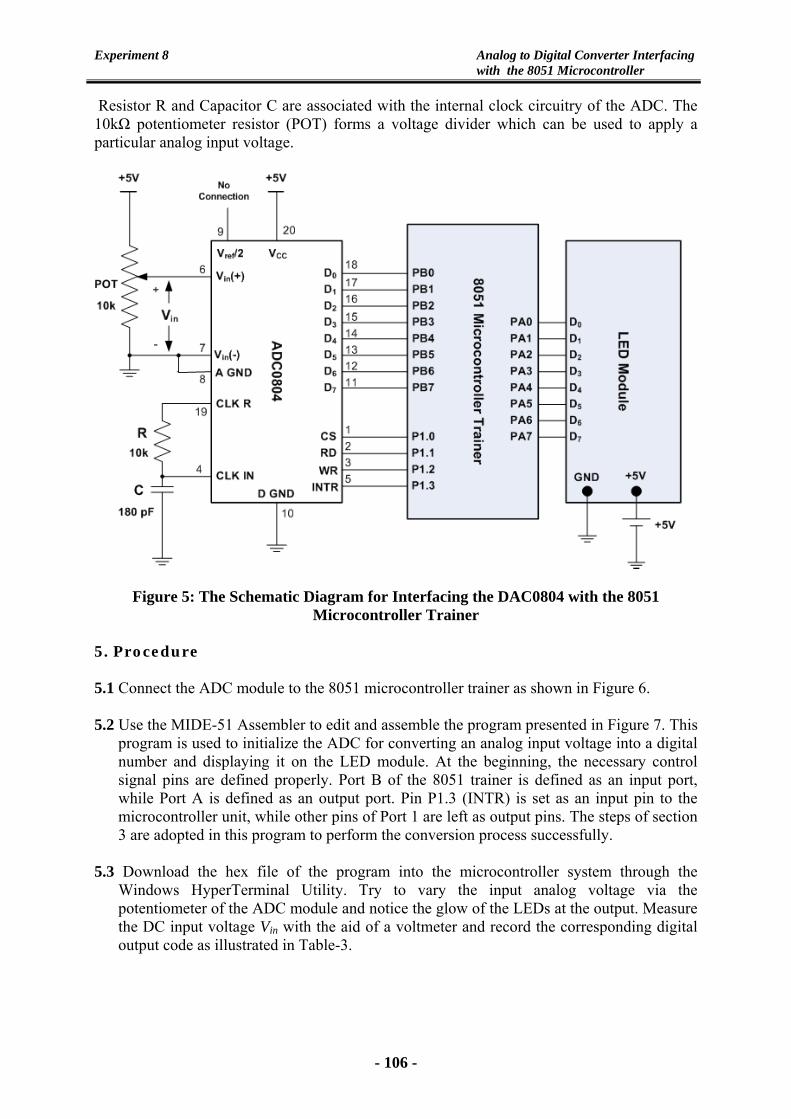
Experiment 8 Analog to Digital Converter Interfacing with the 8051 Microcontroller
Resistor R and Capacitor C are associated with the internal clock circuitry of the ADC. The 10kΩ potentiometer resistor (POT) forms a voltage divider which can be used to apply a particular analog input voltage.
Figure 5: The Schematic Diagram for Interfacing the DAC0804 with the 8051 Microcontroller Trainer
5. Procedure 5.1 Connect the ADC module to the 8051 microcontroller trainer as shown in Figure 6. 5.2 Use the MIDE-51 Assembler to edit and assemble the program presented in Figure 7. This
program is used to initialize the ADC for converting an analog input voltage into a digital number and displaying it on the LED module. At the beginning, the necessary control signal pins are defined properly. Port B of the 8051 trainer is defined as an input port, while Port A is defined as an output port. Pin P1.3 (INTR) is set as an input pin to the microcontroller unit, while other pins of Port 1 are left as output pins. The steps of section 3 are adopted in this program to perform the conversion process successfully.
5.3 Download the hex file of the program into the microcontroller system through the
Windows HyperTerminal Utility. Try to vary the input analog voltage via the potentiometer of the ADC module and notice the glow of the LEDs at the output. Measure the DC input voltage Vin with the aid of a voltmeter and record the corresponding digital output code as illustrated in Table-3.
- 106 -

Experiment 8 Analog to Digital Converter Interfacing with the 8051 Microcontroller
Figure 6: Interfacing the ADC Module with the 8051 Microcontroller Trainer
Table-3: Measured Analog Input Voltage versus Digital Output
Vin(V) Digital Output (Binary) Digital Output (Decimal)
0
0.5
1.0
1.5
2.0
2.5
3.0
3.5
4.0
4.5
5.0
- 107 -

Experiment 8 Analog to Digital Converter Interfacing with the 8051 Microcontroller
ORG 2000H PA EQU 0F800H PB EQU 0F801H PortReg EQU 0F803H ESC EQU 003EH CS EQU P1.0 RDS EQU P1.1 WRS EQU P1.2 INTR EQU P1.3 MOV DPTR,#PortReg MOV A,#82H MOVX @DPTR,A SETB INTR BEGIN: CLR CS SETB RDS CLR WRS SETB WRS WAIT: JB INTR,WAIT CLR CS CLR RDS MOV DPTR,#PB MOVX A,@DPTR MOV DPTR,#PA MOVX @DPTR,A LCALL ESC JC EXIT SJMP BEGIN EXIT: CLR A MOV DPTR,#PA MOVX @DPTR,A HERE: SJMP HERE END
Figure 7: The 8051 Program Used to Convert an Analog Voltage to Digital Code
Exercise Write and run an 8051 program to detect an input voltage equal to 2.5V. Make an LED to glow at the output when Vin = 5V. Hint: Use the CJNE instruction for comparing the content of the accumulator with 255
(Decimal).
- 108 -

Experiment 8 Analog to Digital Converter Interfacing with the 8051 Microcontroller
6. Discussion
1. Determine the step size of a 3-bit ADC if the reference voltage is 8V. 2. Sketch a general block diagram for the successive approximation ADC indicating its
various sub-circuits.
3. Calculate theoretically the digital output for each input voltage magnitude in Table-3 and compare it with the measured quantities.
4. Write an 8051 assembly program to test the value of the input voltage and set an LED
ON if the input is greater than or equal to 2.5V.
Hint: Use the SUBB instruction and check the carry bit for positive or negative result.
5. In the ADC0804, how do you know if the ADC is ready to provide data?
6. For the ADC0804, find the step size for each of the following Vref/2 values:
(a) Vref/2 = 1.28V (b) Vref/2 = 1V (c) Vref/2 = 1.9V 7. With Vref/2 = 0.64V, find the value of the analog input voltage Vin for the following
outputs: (a) Dout = 11111111 (b) Dout = 10011001 (c) Dout = 11011011
8. Give the status of CS and WR in order to start conversion for the ADC0804.
- 109 -

Experiment 8 Analog to Digital Converter Interfacing with the 8051 Microcontroller
This Page is left intentionally blank
- 110 -
Experiment 9 DC Motor Speed Control Using the 8051 Microcontroller
Experiment 9
DC Motor Speed Control Using the 8051 Microcontroller
Objectives The purpose of this experiment is to connect a DC motor module with the 8051 microcontroller trainer and control its speed using the pulse width modulation (PWM) method. 1. Introduction
It is widely needed to control the speed of a DC motor automatically by the microcontroller. In order to implement the interfacing process between a DC motor and the microcontroller, it is required to design an electronic circuit to connect the motor into one of the microcontroller ports. This circuit is utilized to direct the flow of signals outgoing from or incoming to the microcontroller's port. Besides, a program should be written and saved in the microcontroller’s memory to control the motor speed automatically from the port of the microcontroller. 2. Methods of Speed Control There are, in general, three techniques used for DC motor speed control. The choice of the specific method depends on the required application. These methods are the field current control method, input voltage control method, and the pulse width modulation method. 2.1 Field Current Control Method It is well-known that the rotational speed of DC motors is inversely proportional to the magnetic field around their poles. By adding a variable resistance in series with the field winding, the field current and thereby the magnetic flux of poles can be changed. Accordingly, the motor speed can also be varied. However, this method is used in separately excited DC motors and can not be used with permanent magnet motors. 2.2 Input Voltage Control Method The speed of DC motors is dependent on the supply input voltage. When changing the applied voltage, the motor speed can thereby be varied. This method was used to control the speed of a permanent magnet DC motor in a previous work. 2.3 Pulse Width Modulation Method This method is the most efficient one for varying DC motor speed. According to this method, the average value of the applied voltage is changed by applying a pulsed waveform to the motor with variable pulse width as shown in Figure 1. This technique is known as Pulse Width Modulation (PWM). As shown from Figure 1, the average value of the applied voltage increases with the increase in pulse width. Based on this fact, the motor speed can be changed by varying the ratio between the pulse width ton and period time Tperiod of the applied signal. The average value of the applied voltage is given by:
- 111 -

Experiment 9 DC Motor Speed Control Using the 8051 Microcontroller
xmaperiod
onav V
TtV .= (1)
where Vmax is the amplitude of the applied pulse signal.
Figure 1: The Pulse Width Modulation Technique On the other hand, the duty cycle is given by:
100×=period
on
Tt
cycleduty (2)
By changing (modulating) the width of the pulse applied to the DC motor we can increase or decrease the amount of power provided to the motor, thereby increasing or decreasing the motor speed. Notice from Figure 1 that, although the voltage has fixed amplitude, it has a variable duty cycle. That means the wider the pulse, the higher the speed. Figure 2 shows the power provided to the motor for different duty cycles.
Figure 2: PWM Signals with Different Duty Cycles
3. 8051 Microcontroller Based DC Motor Interface Circuit Figure 3 illustrates a driver circuit of a DC motor connected to the 8051 microcontroller trainer to control the speed of a small 5V permanent magnet DC motor using the PWM technique. This circuit contains a solid-state relay (opto-isolator), and a driver transistor to provide the DC motor with the required current for running it.
- 112 -

Experiment 9 DC Motor Speed Control Using the 8051 Microcontroller
The opto-isolator is used to protect the 8051 microcontroller from the motor circuit and to provide a clean and fast switching. It consists of an LED and a phototransistor as shown in Figure 4. The DC motor is connected to a 5V DC supply via the driving transistor. A free-wheeling diode is connected across the DC motor to protect the transistor from any back-induced voltage. The capacitor shown in the circuit is useful to remove the EMI and noise produced during motor operation. When the output signal from the pin of the microcontroller’s port is set HIGH (Logic-1), current passes through the internal LED diode of the opto-isolator and the LED emits light thereby turning the internal phototransistor on, and causing current to flow into the base of the driving transistor. This will turn on the driving transistor and the DC motor.
Figure 3: DC Motor Interface Circuit
Figure 4: The 4N35 Optoisolator Pin Configuration and Equivalent Circuit
- 113 -

Experiment 9 DC Motor Speed Control Using the 8051 Microcontroller
4. Procedure 4.1 Connect the DC motor module with the 8051 microcontroller trainer as shown in Figure 5
below.
Figure 5: Interfacing the DC Motor Module with the 8051 Microcontroller Trainer
4.2 Use the MIDE-51 assembler to enter and assemble the program shown in Figure 6. This program is used to control the speed of the DC motor in three levels depending on the PWM signal generated by the microcontroller at pin PA0. The selection of the required speed is achieved by switches S0 and S1 of the input switch module as depicted in Table-1. Port B is defined as input port, while Port A is defined as an output port. The received signal from port B is masked with the binary number 00000011 using the ANL logic instruction to check the value selected by the user. This value is compared with 00, 01, 02, and 03 to send the appropriate PWM signal into the motor circuit.
Table-1: Control Inputs for Motor Speed Selection
S1 S0 Duty Cycle Motor Speed0 0 0% Standstill 0 1 25% Minimum 1 0 50% Medium 1 1 100% Maximum
4.3 Download the hex file of the program into the microcontroller system through the
HyperTerminal utility and observe the variation of the motor speed. Try to monitor the generated PWM signal at pin PA0 with an oscilloscope for each speed.
- 114 -
Experiment 9 DC Motor Speed Control Using the 8051 Microcontroller
; DC MOTOR SPEED CONTROL ORG 2000H PA EQU 0F800H PB EQU 0F801H PortReg EQU 0F803H ESC EQU 003EH MOV DPTR, #PortReg MOV A, #82H MOVX @DPTR, A BEGIN: MOV DPTR, #PB MOVX A, @DPTR ANL A, #03 CJNE A, #00, SPEED1 MOV DPTR, #PA CLR A MOVX @DPTR, A LCALL ESC JC EXIT SJMP BEGIN SPEED1: CJNE A, #01, SPEED2 MOV DPTR, #PA MOV A, #01 MOVX @DPTR, A ACALL DELAY CLR A MOVX @DPTR, A ACALL DELAY ACALL DELAY ACALL DELAY LCALL ESC JC EXIT SJMP BEGIN SPEED2: CJNE A, #02, SPEED3 MOV DPTR, #PA MOV A, #01 MOVX @DPTR, A ACALL DELAY ACALL DELAY CLR A MOVX @DPTR,A ACALL DELAY ACALL DELAY LCALL ESC JC EXIT SJMP BEGIN SPEED3: MOV DPTR,#PA MOV A,#01
- 115 -

Experiment 9 DC Motor Speed Control Using the 8051 Microcontroller
MOVX @DPTR,A LCALL ESC JC EXIT SJMP BEGIN DELAY: MOV R0, #0FFH H1: NOP DJNZ R0, H1 RET EXIT: CLR A MOV DPTR, #PA MOVX @DPTR, A HERE: SJMP HERE END
Figure 6: The 8051 Assembly Program Used to Control the Speed of the DC Motor
Exercise Write and run an 8051 program to rotate the DC motor with a speed of 10% duty cycle and stop it from a single switch. 5. Discussion
1. Calculate the average voltage provided to the DC motor for each speed indicated in Table-1.
2. State the main differences between mechanical relays and solid state relays used in
motor driving circuits.
3. Discuss the different techniques used in DC motor speed control?
4. Develop an 8051 program to vary the speed of the DC motor in 7 levels from three switches.
5. Suggest a DC motor direction control circuit and explain its operation.
6. State the major differences between DC motors and stepper motors.
- 116 -

Experiment 10 The 8051 Microcontroller Based System Design
Experiment 10
The 8051 Microcontroller Based System Design
Objectives The purpose of this experiment is to learn building and programming simple stand-alone microcontroller-based systems. Required Instruments and Parts
1- Atmel AT89C51 or AT89C52 microcontroller chip. 2- Universal IC programmer such as the DATAMAN 40-Pro. 3- DC Power Supply. 4- Digital Storage Oscilloscope. 5- Bread-boards. 6- 10 MHz crystal. 7- Push-button micro-switch. 8- Capacitors: 2 × 22 pF, 10 µF. 9- Resistors 4 × 470Ω, 8.2 kΩ. 10- 4 LEDs.
1. Introduction Microcontrollers can be used in embedded systems to perform certain tasks. Before connecting the 8051 microcontroller in the proposed system, an assembly program should first be written and converted into a hex file using a certain assembler. This file is then burned inside the code memory of the 8051 chip by means of a programmer. The complexity of the 8051-based system depends on the required task to be performed. In the procedure of this experiment, we will illustrate how to program the 8051 microcontroller chip and use it in simple circuits. 2. Procedure 2.1 Use the MIDE-51 assembler to enter and assemble the program listed in Figure 1. This
program is used to produce a moving bit sequence at 4 LEDs connected to Port 1 of the AT89C51 microcontroller chip. Save this file with the name mbit.asm. The generated hex file should have the name mbit.hex.
2.2 Try to burn the generated hex file inside the code memory of the 8051 chip. First of all,
turn off the programmer and fix the AT89C51 IC in its socket properly. 2.3 Connect the universal programmer into the PC via a USB cable and turn it on.
- 117 -

Experiment 10 The 8051 Microcontroller Based System Design
; Program to generate a moving-bit sequence ORG 00H MOV A, #11H START: MOV P1, A RL A ACALL DELAY SJMP START HERE: SJMP HERE DELAY: MOV R0, #05 L1: MOV R1, #255 L2: MOV R2, #255 L3: DJNZ R2, L3 DJNZ R1, L2 DJNZ R0, L1 RET END
Figure 1: An 8051 Program to Generate a Moving Bit Sequence
2.4 Run the software of the universal programmer by double-clicking on its icon (Dataman-
Pro Pg4uw). A startup window appears as shown in Figure 2 below.
Figure 2: The Startup Window of the Dataman Programmer’s Software
- 118 -
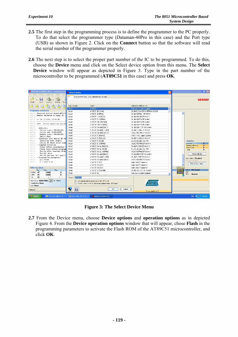
Experiment 10 The 8051 Microcontroller Based System Design
2.5 The first step in the programming process is to define the programmer to the PC properly.
To do that select the programmer type (Dataman-40Pro in this case) and the Port type (USB) as shown in Figure 2. Click on the Connect button so that the software will read the serial number of the programmer properly.
2.6 The next step is to select the proper part number of the IC to be programmed. To do this,
choose the Device menu and click on the Select device option from this menu. The Select Device window will appear as depicted in Figure 3. Type in the part number of the microcontroller to be programmed (AT89C51 in this case) and press OK.
Figure 3: The Select Device Menu
2.7 From the Device menu, choose Device options and operation options as in depicted Figure 4. From the Device operation options window that will appear, chose Flash in the programming parameters to activate the Flash ROM of the AT89C51 microcontroller, and click OK.
- 119 -

Experiment 10 The 8051 Microcontroller Based System Design
Figure 4: Choosing Device Options
Figure 5: The Device Operation Options Window
2.8 The next step is to load the hex file into the buffer memory of the software. This can be
done by clicking on the Load icon in the tools bar, or by selecting the command Load from the file menu. Select the hex file from the window which appears and click Open as shown in Figure 6. The loaded hex file can be viewed or edited in the buffer memory by
- 120 -

Experiment 10 The 8051 Microcontroller Based System Design
clicking on the View/Edit icon on the tools bar or choosing the View/Edit command from the Buffer menu.
Figure 6: The Load File Window
Figure 7: The Buffer Memory
- 121 -

Experiment 10 The 8051 Microcontroller Based System Design
2.9 To burn the hex file in the microcontroller’s flash memory, click on the Program icon on
the tools bar, or select the command Program from the Device menu. After that, select the Verify command from the Device menu for burning verification. The flash memory of the microcontroller can be checked using the Read command of the Device menu. The flash ROM of the chip can be erased using the Erase command in the same menu.
2.10 After programming the microcontroller chip, connect the circuit shown in Figure 8 on a
breadboard. Confirm the operation of this circuit by noticing the glowing of the LEDs.
Figure 8: An 8051 Microcontroller Circuit for Driving 4 LEDs
2.11 Use the MIDE-51 assembler to edit and assemble the program of Figure 9. This program
is used to generate a square wave from pin P1.0. Burn the hex file of the program into the flash memory of the microcontroller after erasing it.
2.12 Connect the circuit of Figure 10 and display the generated signal on the oscilloscope.
- 122 -

Experiment 10 The 8051 Microcontroller Based System Design
ORG 00H BEGIN: SETB P1.0 ACALL DELAY CLR P1.0 ACALL DELAY SJMP BEGIN HERE: SJMP HERE DELAY: MOV R0, #0FH L1: DJNZ R0, L1 RET END
Figure 9: Program to Generate a Square Wave
Figure 10: An 8051 Microcontroller Circuit to Generate a Square Wave
- 123 -

Experiment 10 The 8051 Microcontroller Based System Design
3. Discussion
1- Modify the program listed in Figure 2 to toggle the 4 LEDs connected to port 1 periodically with a certain delay time.
2- Calculate the delay time for the delay subroutine in the program of Figure 1 knowing
that the DJNZ instruction takes 2 machine cycles in the 89C51 microcontroller.
3- Modify the program of Figure 9 to generate a pulse signal with a duty cycle of 66%.
4- For the 8051 microcontroller system shown below, write a program to implement a digital counter that counts from 0 to 9 on the seven segment display. Refer to experiment 5 for more details about 7-segment displays.
Interfacing a 7-Segment Display with the 8051 Microcontroller
5- Design a microcontroller system to control the direction of rotation of a small
permanent magnet DC motor using a transistor H-Bridge circuit. Write the necessary 8051 assembly file to run the motor in either direction.
6- Modify the circuit of Figure 8 by adding a control switch at pin P2.0. If the switch is
ON, then the moving bit is shifting from right to left across the 4 LEDs, and if the switch is OFF, then the moving bit is shifting from left to right. Sketch the new circuit diagram and write the necessary software for doing this task.
- 124 -

References
1. Muhammed Ali Mazidi and Janice J. Mazidi, The 80x86 PC & Compatible Computers, Prentice Hall, 2nd edition, 1998.
2. Muhammad Ali Mazidi, Janice G. Mazidi, and Rolin D. McKinlay, The 8051
Microcontroller and Embedded Systems Using Assembly and C, 2nd Edition, Prentice-Hall, New-Delhi, India, 2006.
3. Kenneth J. Ayala, The 8051 Microcontroller Architecture, Programming, and
Applications, West Publishing Company, USA, 1991.
4. I. Scott MacKenzie, The 8051 Microcontroller, 2nd Edition, Prentice-Hall, USA, 1995.
5. Firas M. Ali, “Stepper Motor Control Using the IBM PC”, Paper presented at the Third National Conference on Basic Science, Al-Jabal Al-Gharbi University, Gharyan, Libya, 25-27/4/2009.
6. Firas M. Ali, "Control a DC Motor with Your PC", Design Idea published at the EDN
Magazine, Vol. 55, No. 16, 26 August 2010, pp. 41-42, www.edn.com.
7. Firas M. Ali, “Design and Implementation of an Interface Circuit for Motor Speed Control Using the PWM Technique”, Engineering & Technology Journal, Vol. 31, No. 6, 2013, pp. 1204-1212.
8. The Web Site, www.8052.com
9. The Web Site, www.micro-digital.net
10. The Web Site, www.mikroe.com
11. The Web Site, www.pjrc.com
12. The Web Site, www.8051projects.info
13. The Web Site, www.microdigitaled.com
14. The Web Site, www.circuitstoday.com
- 125 -

This page is left intentionally blank
- 126 -

The 8051 Microcontroller Architecture
Appendix-A
Appendix-A
The 8051 Microcontroller Architecture This appendix is added to review the internal architecture of the 8051 microcontroller and its organization. Understanding it is very necessary for implementing the experiments associated with the 8051 microcontroller. A.1 Introduction A microcontroller (µC) is a single integrated circuit that executes a user program, normally for the purpose of controlling some device – hence the name microcontroller. A microcontroller has a CPU in addition to a fixed amount of RAM, ROM, I/O ports, serial port, and a timer all on a single chip. Microcontrollers are found in devices such as microwave ovens, automobiles, keyboards, CD players, cell phones, security systems, electronic toys, garage door openers, answering machines, lighting control, … etc. These are devices that require some amount of computing power, but don't require so much as to justify the use of a more complex microprocessor based system which generally requires a large amount of supporting circuitry and memory. Microcontroller-based systems are generally physically smaller, more reliable, and cheaper than the PC-based systems. They are ideal for the types of applications where unit cost and size are very important considerations.
Figure 1: Difference between the Microprocessor and the Microcontroller
- 127 -
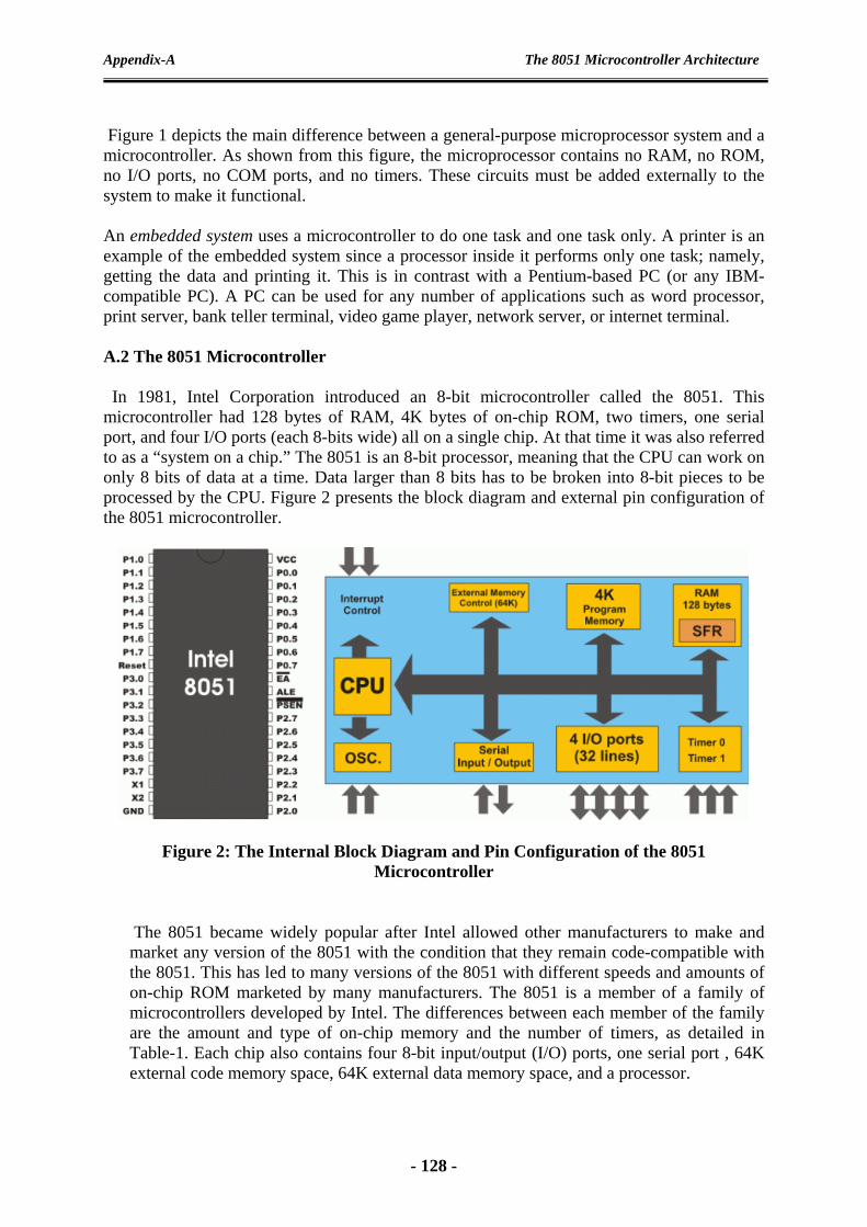
The 8051 Microcontroller Architecture
Appendix-A
Figure 1 depicts the main difference between a general-purpose microprocessor system and a microcontroller. As shown from this figure, the microprocessor contains no RAM, no ROM, no I/O ports, no COM ports, and no timers. These circuits must be added externally to the system to make it functional. An embedded system uses a microcontroller to do one task and one task only. A printer is an example of the embedded system since a processor inside it performs only one task; namely, getting the data and printing it. This is in contrast with a Pentium-based PC (or any IBM-compatible PC). A PC can be used for any number of applications such as word processor, print server, bank teller terminal, video game player, network server, or internet terminal. A.2 The 8051 Microcontroller In 1981, Intel Corporation introduced an 8-bit microcontroller called the 8051. This microcontroller had 128 bytes of RAM, 4K bytes of on-chip ROM, two timers, one serial port, and four I/O ports (each 8-bits wide) all on a single chip. At that time it was also referred to as a “system on a chip.” The 8051 is an 8-bit processor, meaning that the CPU can work on only 8 bits of data at a time. Data larger than 8 bits has to be broken into 8-bit pieces to be processed by the CPU. Figure 2 presents the block diagram and external pin configuration of the 8051 microcontroller.
Figure 2: The Internal Block Diagram and Pin Configuration of the 8051 Microcontroller
The 8051 became widely popular after Intel allowed other manufacturers to make and market any version of the 8051 with the condition that they remain code-compatible with the 8051. This has led to many versions of the 8051 with different speeds and amounts of on-chip ROM marketed by many manufacturers. The 8051 is a member of a family of microcontrollers developed by Intel. The differences between each member of the family are the amount and type of on-chip memory and the number of timers, as detailed in Table-1. Each chip also contains four 8-bit input/output (I/O) ports, one serial port , 64K external code memory space, 64K external data memory space, and a processor.
- 128 -

The 8051 Microcontroller Architecture
Appendix-A
The user program is burned into the on-chip ROM of the microcontroller. There are different types of ROMs such as PROM, UV-EPROM, EEPROM, Flash ROM, and NV-RAM. They differ in the method of programming and the time of erasing and burning.
Table-1: Comparison of the 8051 Family Members
Microcontroller On-chip ROM On-chip RAM Timers 8051 4K ROM 128 bytes 2 8031 0 128 bytes 2 8751 4K EPROM 128 bytes 2 8951 4K Flash ROM 128 bytes 2 8052 8K ROM 256 bytes 3 8032 0 256 bytes 3 8752 8K EPROM 256 bytes 3 8952 8K Flash ROM 256 bytes 3
As can be seen from Table-1, the 8051 is a subset of the 8052; therefore, all programs written for the 8051 will run on the 8052, but the reverse is not true. Figure 2 shows the 8051 microcontroller chip housed in a 40-pin DIP package. The pins description is as follows:
Pins 1-8 ( Port 1) : Each of these pins can be configured as an input or an output.
Pin 9 (RST): A logic one on this pin disables the microcontroller and clears the contents of most registers. In other words, the positive voltage on this pin resets the microcontroller. By applying logic zero to this pin, the program starts execution from the beginning.
Pins 10-17 (Port 3): Similar to port 1, each of these pins can serve as general input or output. Besides, all of them have alternative functions:
Pin 10 (RXD): Serial asynchronous communication input or Serial synchronous communication output.
Pin 11 (TXD): Serial asynchronous communication output or Serial synchronous communication clock output.
Pin 12 (INT0): Interrupt 0 input.
Pin 13 (INT1): Interrupt 1 input.
Pin 14 (T0): Counter 0 clock input.
Pin 15 (T1): Counter 1 clock input.
Pin 16 (WR): Write to external (additional) RAM.
Pin 17 (RD): Read from external RAM.
- 129 -
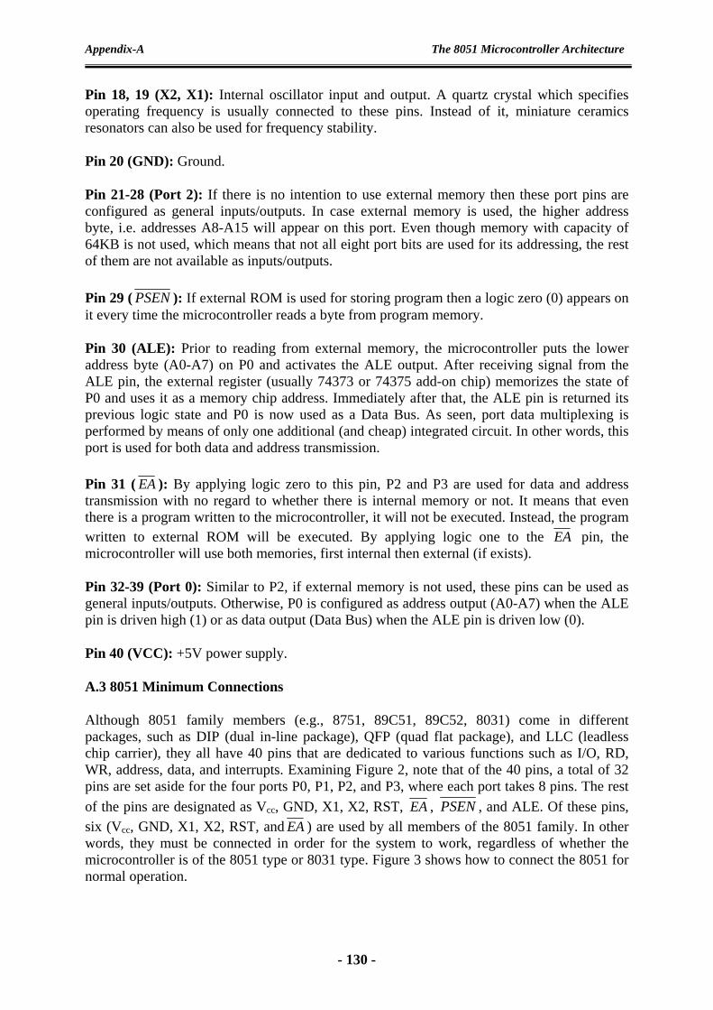
The 8051 Microcontroller Architecture
Appendix-A
Pin 18, 19 (X2, X1): Internal oscillator input and output. A quartz crystal which specifies operating frequency is usually connected to these pins. Instead of it, miniature ceramics resonators can also be used for frequency stability.
Pin 20 (GND): Ground.
Pin 21-28 (Port 2): If there is no intention to use external memory then these port pins are configured as general inputs/outputs. In case external memory is used, the higher address byte, i.e. addresses A8-A15 will appear on this port. Even though memory with capacity of 64KB is not used, which means that not all eight port bits are used for its addressing, the rest of them are not available as inputs/outputs.
Pin 29 ( PSEN ): If external ROM is used for storing program then a logic zero (0) appears on it every time the microcontroller reads a byte from program memory.
Pin 30 (ALE): Prior to reading from external memory, the microcontroller puts the lower address byte (A0-A7) on P0 and activates the ALE output. After receiving signal from the ALE pin, the external register (usually 74373 or 74375 add-on chip) memorizes the state of P0 and uses it as a memory chip address. Immediately after that, the ALE pin is returned its previous logic state and P0 is now used as a Data Bus. As seen, port data multiplexing is performed by means of only one additional (and cheap) integrated circuit. In other words, this port is used for both data and address transmission.
Pin 31 ( EA ): By applying logic zero to this pin, P2 and P3 are used for data and address transmission with no regard to whether there is internal memory or not. It means that even there is a program written to the microcontroller, it will not be executed. Instead, the program written to external ROM will be executed. By applying logic one to the EA pin, the microcontroller will use both memories, first internal then external (if exists).
Pin 32-39 (Port 0): Similar to P2, if external memory is not used, these pins can be used as general inputs/outputs. Otherwise, P0 is configured as address output (A0-A7) when the ALE pin is driven high (1) or as data output (Data Bus) when the ALE pin is driven low (0).
Pin 40 (VCC): +5V power supply.
A.3 8051 Minimum Connections
Although 8051 family members (e.g., 8751, 89C51, 89C52, 8031) come in different packages, such as DIP (dual in-line package), QFP (quad flat package), and LLC (leadless chip carrier), they all have 40 pins that are dedicated to various functions such as I/O, RD, WR, address, data, and interrupts. Examining Figure 2, note that of the 40 pins, a total of 32 pins are set aside for the four ports P0, P1, P2, and P3, where each port takes 8 pins. The rest of the pins are designated as Vcc, GND, X1, X2, RST, EA , PSEN , and ALE. Of these pins, six (Vcc, GND, X1, X2, RST, and EA ) are used by all members of the 8051 family. In other words, they must be connected in order for the system to work, regardless of whether the microcontroller is of the 8051 type or 8031 type. Figure 3 shows how to connect the 8051 for normal operation.
- 130 -

The 8051 Microcontroller Architecture
Appendix-A
Figure 3: 8051 Oscillator and Reset Circuit Connections
The 8051 has an on-chip oscillator but requires an external clock to run it. Most often a quartz crystal oscillator is connected to inputs X1 (pin 19) and X2 (pin 18). The quartz crystal oscillator connected to X1 and X2 also needs two capacitors of 30 pF value. One side of each capacitor is connected to the ground as shown in Figure 3. The frequency of the crystal connected to the 8051 family can vary from 4 MHz to 30 MHz, depending on the chip rating and manufacturer. Speed refers to the maximum oscillator frequency connected to the crystal. When the 8051 is connected to a crystal oscillator and is powered up, we can observe the frequency on the X2 pin using the oscilloscope. The CPU takes a certain number of clock cycles to execute an instruction. In the 8051 family, these clock cycles are referred to as machine cycles. In the original 8051, one machine cycle takes 12 oscillator periods. Therefore, to calculate the machine cycle for the 8051, we take 1/12 of the crystal frequency; then take its inverse. Pin 9 is the RESET pin. It is an input and is active high (normally low). Upon applying a high pulse to this pin, the microcontroller will reset and terminate all activities. This is often referred to as a power-on reset. Activating a power-on reset will cause all values in the registers to be lost. It will set program counter to all 0s. Figure 3 shows the way of connecting the RST pin to the power-on reset circuitry using a momentary switch. In order for the RESET input to be effective, it must have a minimum duration of two machine cycles. In other words, the high pulse must be high for a minimum of two machine cycles before it is allowed to go low. A.4 8051 Memory Organization The 8051 has two types of memory which are Program Memory and Data Memory. Program Memory (or code memory) is used to save the program being executed, while Data Memory is used for storing data and intermediate results created and used during the operation of the microcontroller. Code memory is usually implemented as ROM for permanent program storage, but it can also be external RAM for program testing purposes. Data memory can either be RAM for temporary storage, or even be ROM for permanent storage of date. RAM
- 131 -

The 8051 Microcontroller Architecture
Appendix-A
and ROM memories in the 8051 microcontroller system are either internal or external as shown in Figure 4. A.4.1 On-chip RAM The 8051 includes a certain amount of on-chip memory. On-chip RAM is really one of two types: Internal RAM and Special Function Register (SFR) memory. The layout of the 8051's internal RAM memory is presented in Figure 5.
Figure 4: 8051 Memory Organization
Figure 5: The Memory Map of the 8051 On-chip RAM
- 132 -

The 8051 Microcontroller Architecture
Appendix-A
There are 128 bytes of RAM in the 8051 (some members, notably the 8052, have 256 bytes of RAM). The 128 bytes of RAM inside the 8051 are assigned addresses 00 to 7FH. These addresses can be accessed directly as memory locations. These 128 bytes are divided into three different groups as follows: 1. A total of 32 bytes from locations 00 to 1F hex are set aside for register banks. The first 8
bytes (00h – 07H) are "register bank 0". By manipulating certain SFRs, a program may choose to use register banks 1, 2, or 3. These alternative register banks are located in internal RAM in addresses 08h through 1FH.
2. A total of 16 bytes from locations 20H to 2FH are set aside for bit-addressable read/write memory.
3. A total of 80 bytes from locations 30H to 7FH are used for read and write storage, or what is normally called a general user RAM. These 80 locations of RAM are widely used for the purpose of storing data and parameters by 8051 programmers.
4. Memory locations from 80H to FFH are called Special Function Registers (SFRs). Special Function Registers (SFRs) are areas of memory that control specific functionality of the 8051 processor. For example, four SFRs permit access to the 8051s 32 input/output lines. Another SFR allows a program to read or write to the 8051s serial port. Other SFRs allow the user to set the serial baud rate, control and access timers, and configure the 8051s interrupt system. SFRs are accessed as if they were normal Internal RAM. The only difference is that Internal RAM is from address 00H through 7FH whereas SFR registers exist in the address range of 80H through FFH. Not all addresses above 80H are assigned to SFRs. However, this area may not be used as additional RAM memory even if a given address has not been assigned to an SFR.
A.4.2 On-chip ROM
On-Chip ROM refers to the code or program memory that physically exists on the microcontroller itself. On-chip ROM can be of several types and with different sizes, depending on the version of the microcontroller as presented in Table-1. Code memory is the memory that holds the actual 8051 program that is to be run. Code memory may be found on-chip, either burned into the microcontroller as ROM or EPROM, or may also be stored completely off-chip in an external ROM or, more commonly, an external EPROM.
Some family members have only 4K bytes of on-chip ROM (e.g., 8751, 8951) and some, such as the 8752, have 8K bytes of ROM. The point to remember is that no member of the 8051 family can access more than 64K bytes of OPCODE since the program counter in the 8051 is a 16-bit register (0000 to FFFF address range). It must be noted that while the first location of program ROM inside the 8051 has the address of 0000, the last location can be different depending on the size of the ROM on the chip. Among the 8051 family members, the 8751 and 8951 have 4K bytes of on-chip ROM. This 4K bytes of ROM memory has memory addresses of 0000 to 0FFFH. Therefore, the first location of on-chip ROM of this 8051 has an address of 0000 and the last location has the address of 0FFFH. Figure 6 shows the ROM address space for some versions of the 8051 microcontroller.
- 133 -
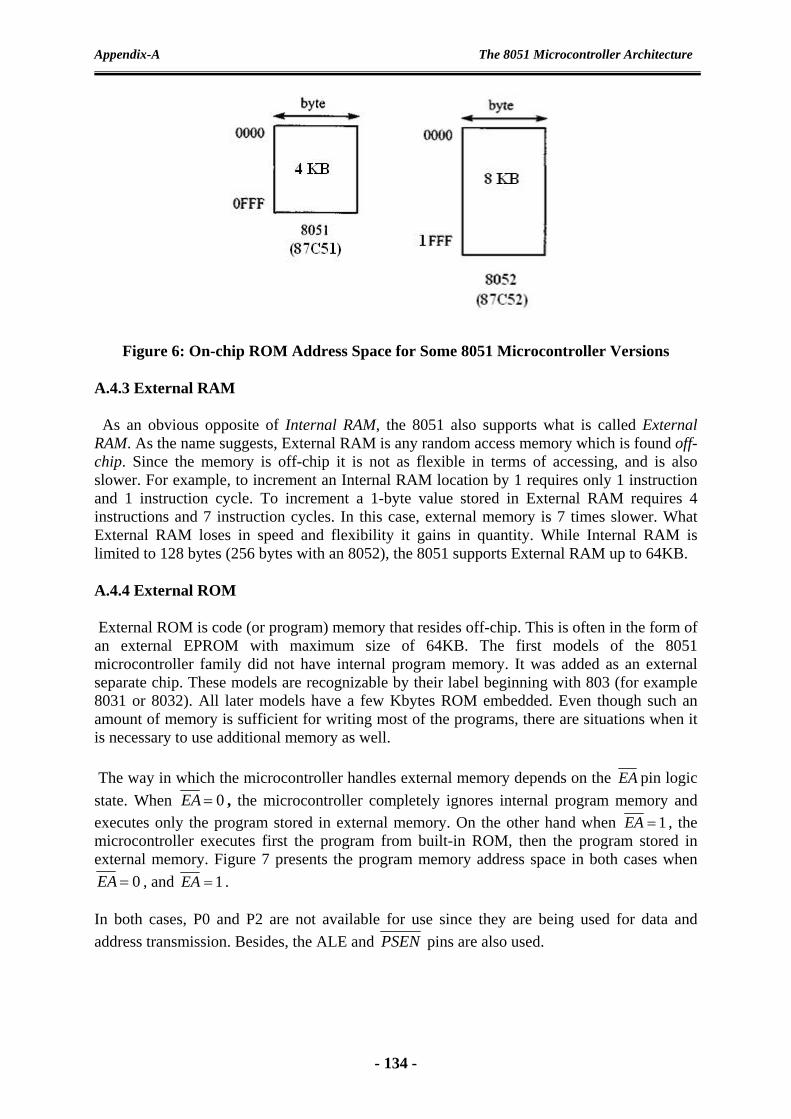
The 8051 Microcontroller Architecture
Appendix-A
Figure 6: On-chip ROM Address Space for Some 8051 Microcontroller Versions
A.4.3 External RAM
As an obvious opposite of Internal RAM, the 8051 also supports what is called External RAM. As the name suggests, External RAM is any random access memory which is found off-chip. Since the memory is off-chip it is not as flexible in terms of accessing, and is also slower. For example, to increment an Internal RAM location by 1 requires only 1 instruction and 1 instruction cycle. To increment a 1-byte value stored in External RAM requires 4 instructions and 7 instruction cycles. In this case, external memory is 7 times slower. What External RAM loses in speed and flexibility it gains in quantity. While Internal RAM is limited to 128 bytes (256 bytes with an 8052), the 8051 supports External RAM up to 64KB.
A.4.4 External ROM
External ROM is code (or program) memory that resides off-chip. This is often in the form of an external EPROM with maximum size of 64KB. The first models of the 8051 microcontroller family did not have internal program memory. It was added as an external separate chip. These models are recognizable by their label beginning with 803 (for example 8031 or 8032). All later models have a few Kbytes ROM embedded. Even though such an amount of memory is sufficient for writing most of the programs, there are situations when it is necessary to use additional memory as well.
The way in which the microcontroller handles external memory depends on the EA pin logic state. When 0=EA , the microcontroller completely ignores internal program memory and executes only the program stored in external memory. On the other hand when 1=EA , the microcontroller executes first the program from built-in ROM, then the program stored in external memory. Figure 7 presents the program memory address space in both cases when
0=EA , and 1=EA .
In both cases, P0 and P2 are not available for use since they are being used for data and address transmission. Besides, the ALE and PSEN pins are also used.
- 134 -

The 8051 Microcontroller Architecture
Appendix-A
Figure 7: Program Memory Address Space
A.4.5 Memory Expansion
In case memory (RAM or ROM) built in the microcontroller is not sufficient, it is possible to add two external memory chips with capacity of 64KB each. P2 and P3 I/O ports are used for their addressing and data transmission. Since the PC (program counter) of the 8031/51 is 16-bit, it is capable of accessing up to 64K bytes of program code. In the 8031/51, port 0 and port 2 provide the 16-bit address to access external memory. Of these two ports, P0 provides the lower 8 bit addresses A0 – A7, and P2 provides the upper 8 bit addresses A8 – A15. More importantly, P0 is also used to provide the 8-bit data bus D0 – D7. In other words, pins P0.0 – P0.7 are used for both the address and data paths. This is called address/data multiplexing in chip design. Of course the reason Intel used address/data multiplexing in the 8031/51 is to save pins. How do we know when P0 is used for the data path and when it is used for the
- 135 -

The 8051 Microcontroller Architecture
Appendix-A
address path? This is the job of the ALE (address latch enable) pin. ALE is an output pin for the 8031/51 microcontroller. Therefore, when ALE = 0 the 8031 uses P0 for the data path, and when ALE = 1, it uses it for the address path. As a result, to extract the addresses from the P0 pins we connect P0 to a 74LS373 D-latch and use the ALE pin to latch the address as shown in Figure 8. This extracting of addresses from P0 is called address/data de-multiplexing. From Figure 8, it is important to note that normally ALE = 0, and P0 is used as a data bus, sending data out or bringing data in. Whenever the 8031/51 wants to use P0 as an address bus, it puts the addresses A0 – A7 on the P0 pins and activates ALE = 1 to indicate that P0 has the addresses. Another important signal for the 8031/51 is the PSEN (program store enable) signal. PSEN is an output signal for the 8031/51 microcontroller and must be connected to the OE pin of a ROM containing the program code. In other words, to access external ROM containing program code, the 8031/51 uses the PSEN signal.
Figure 8: 8051 Connections to External Memory
A.5 Special Function Registers (SFRs)
The 8051 is a flexible microcontroller with a relatively large number of modes of operations. The program may inspect and/or change the operating mode of the 8051 by manipulating the values of the 8051's Special Function Registers (SFRs).
SFRs are accessed as if they were normal Internal RAM. The only difference is that Internal RAM is from address 00H through 7FH whereas SFR registers exist in the address range of 80H through FFH.
- 136 -

The 8051 Microcontroller Architecture
Appendix-A
Each SFR has an address (80H through FFH) and a name. The chart in Figure 9 provides a graphical presentation of the 8051's SFRs, their names, and their addresses.
Figure 9: The Special Function Registers of the 8051 Microcontroller
As can be seen from Fig.9, although the address range of 80H through FFH offer 128 possible addresses, there are only 21 SFRs in a standard 8051. All other addresses in the SFR range (80H through FFH) are considered invalid. Writing to or reading from these registers may produce undefined values or behavior. The registers with dark background in Fig.9 are bit addressable registers, which means that the user can access each bit in those registers.
The following is a general description for each of the special function registers:
P0 (Port 0, Address 80H, Bit-Addressable): This is input/output port 0. Each bit of this SFR corresponds to one of the pins on the microcontroller. For example, bit 0 of port 0 is pin P0.0, bit 7 is pin P0.7. Writing a value of 1 to a bit of this SFR will send a high level on the corresponding I/O pin whereas a value of 0 will bring it to a low level.
SP (Stack Pointer, Address 81H): This is the stack pointer of the microcontroller. This SFR indicates where the next value to be taken from the stack will be read from Internal RAM. If you push a value onto the stack, the value will be written to the address of SP + 1. That is to say, if SP holds the value 07H, a PUSH instruction will push the value onto the stack at address 08h. This SFR is modified by all instructions which modify the stack, such as PUSH, POP, LCALL, RET, RETI, and whenever interrupts are invoked by the microcontroller. DPL/DPH (Data Pointer Low/High, Addresses 82H/83H): The SFRs DPL and DPH work together to represent a 16-bit value called the Data Pointer. The data pointer is used in operations regarding external RAM and some instructions involving code memory. Since it is an unsigned two-byte integer value, it can represent values from 0000H to FFFFH (0 through 65,535 decimal).
- 137 -

The 8051 Microcontroller Architecture
Appendix-A
PCON (Power Control, Addresses 87H): The Power Control SFR is used to control the 8051's power control modes. Certain operation modes of the 8051 allow the 8051 to go into a type of "sleep" mode which requires much less power. These modes of operation are controlled through PCON. Additionally, one of the bits in PCON is used to double the effective baud rate of the 8051's serial port.
TCON (Timer Control, Addresses 88H, Bit-Addressable): The Timer Control SFR is used to configure and modify the way in which the 8051's two timers operate. This SFR controls whether each of the two timers is running or stopped and contains a flag to indicate that each timer has overflowed. Additionally, some non-timer related bits are located in the TCON SFR. These bits are used to configure the way in which the external interrupts are activated and also contain the external interrupt flags which are set when an external interrupt has occurred.
TMOD (Timer Mode, Addresses 89H): The Timer Mode SFR is used to configure the mode of operation of each of the two timers. Using this SFR your program may configure each timer to be a 16-bit timer, an 8-bit autoreload timer, a 13-bit timer, or two separate timers. Additionally, you may configure the timers to only count when an external pin is activated or to count "events" that are indicated on an external pin.
TL0/TH0 (Timer 0 Low/High, Addresses 8AH/8CH): These two SFRs, taken together, represent timer 0. Their exact behavior depends on how the timer is configured in the TMOD SFR; however, these timers always count up. What is configurable is how and when they increment in value.
TL1/TH1 (Timer 1 Low/High, Addresses 8BH/8DH): These two SFRs, taken together, represent timer 1. Their exact behavior depends on how the timer is configured in the TMOD SFR; however, these timers always count up. What is configurable is how and when they increment in value.
P1 (Port 1, Address 90H, Bit-Addressable): This is input/output port 1. Each bit of this SFR corresponds to one of the pins on the microcontroller. For example, bit 0 of port 1 is pin P1.0, bit 7 is pin P1.7. Writing a value of 1 to a bit of this SFR will send a high level on the corresponding I/O pin whereas a value of 0 will bring it to a low level.
SCON (Serial Control, Addresses 98H, Bit-Addressable): The Serial Control SFR is used to configure the behavior of the 8051's on-board serial port. This SFR controls the baud rate of the serial port, whether the serial port is activated to receive data, and also contains flags that are set when a byte is successfully sent or received.
SBUF (Serial Buffer, Addresses 99H): The Serial Buffer SFR is used to send and receive data via the on-board serial port. Any value written to SBUF will be sent out the serial port's TXD pin. Likewise, any value which the 8051 receives via the serial port's RXD pin will be delivered to the user program via SBUF. In other words, SBUF serves as the output port when written to and as an input port when read from.
P2 (Port 2, Address A0H, Bit-Addressable): This is input/output port 2. Each bit of this SFR corresponds to one of the pins on the microcontroller. For example, bit 0 of port 2 is pin P2.0, bit 7 is pin P2.7. Writing a value of 1 to a bit of this SFR will send a high level on the corresponding I/O pin whereas a value of 0 will bring it to a low level.
- 138 -

The 8051 Microcontroller Architecture
Appendix-A
IE (Interrupt Enable, Addresses A8H): The Interrupt Enable SFR is used to enable and disable specific interrupts. The low 7 bits of the SFR are used to enable/disable the specific interrupts, whereas the highest bit is used to enable or disable ALL interrupts. Thus, if the high bit of IE is 0 all interrupts are disabled regardless of whether an individual interrupt is enabled by setting a lower bit.
P3 (Port 3, Address B0h, Bit-Addressable): This is input/output port 3. Each bit of this SFR corresponds to one of the pins on the microcontroller. For example, bit 0 of port 3 is pin P3.0, bit 7 is pin P3.7. Writing a value of 1 to a bit of this SFR will send a high level on the corresponding I/O pin whereas a value of 0 will bring it to a low level.
IP (Interrupt Priority, Addresses B8H, Bit-Addressable): The Interrupt Priority SFR is used to specify the relative priority of each interrupt. On the 8051, an interrupt may either be of low (0) priority or high (1) priority. An interrupt may only interrupt interrupts of lower priority. For example, if we configure the 8051 so that all interrupts are of low priority except the serial interrupt, the serial interrupt will always be able to interrupt the system, even if another interrupt is currently executing. However, if a serial interrupt is executing no other interrupt will be able to interrupt the serial interrupt routine since the serial interrupt routine has the highest priority.
PSW (Program Status Word, Addresses D0H, Bit-Addressable): The Program Status Word is used to store a number of important bits that are set and cleared by 8051 instructions. The PSW SFR contains the carry flag, the auxiliary carry flag, the overflow flag, and the parity flag. Additionally, the PSW register contains the register bank select flags which are used to select which of the "R" register banks are currently selected.
A (Accumulator, Addresses E0H, Bit-Addressable): The Accumulator (Register A) is one of the most-used SFRs on the 8051 since it is involved in so many instructions. The Accumulator resides as an SFR at E0H, which means the instruction MOV A,#20H is really the same as MOV 0E0H,#20H. However, it is a good idea to use the first method since it only requires two bytes whereas the second option requires three bytes.
B (B Register, Addresses F0H, Bit-Addressable): The "B" register is used in two instructions: the multiply and divide operations. The B register is also commonly used by programmers as an auxiliary register to temporarily store values.
A.6 Basic Registers
The most widely used registers of the 8051 are A (accumulator), B, R0, R1, R2, R3, R4, R5, R6, R7, DPTR (data pointer), and PC (program counter). All of the above registers are 8-bits, except DPTR and the program counter. Figure 10 presents these registers.
A.6.1 The Accumulator
The Accumulator, as its name suggests, is used as a general register to accumulate the results of a large number of instructions. It can hold an 8-bit (1-byte) value and is the most versatile register the 8051 has due to the shear number of instructions that make use of the accumulator. More than half of the 8051s 255 instructions manipulate or use the accumulator in some way.
- 139 -
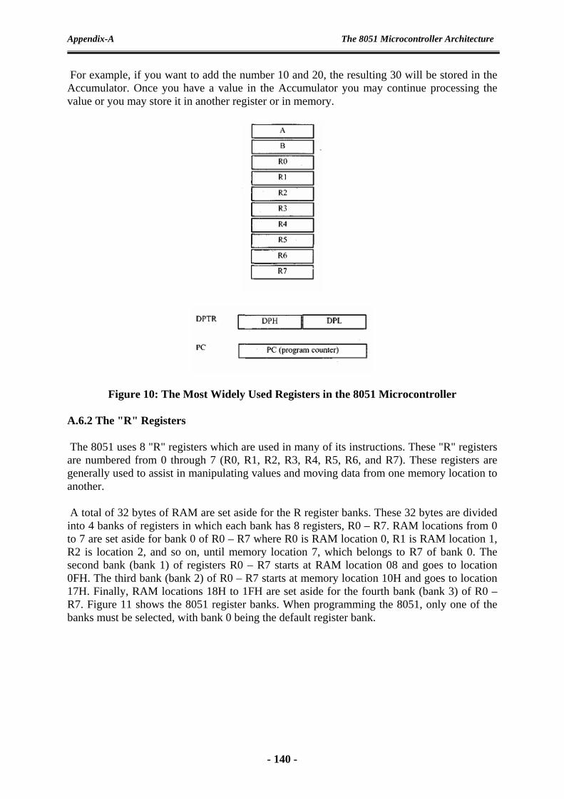
The 8051 Microcontroller Architecture
Appendix-A
For example, if you want to add the number 10 and 20, the resulting 30 will be stored in the Accumulator. Once you have a value in the Accumulator you may continue processing the value or you may store it in another register or in memory.
Figure 10: The Most Widely Used Registers in the 8051 Microcontroller
A.6.2 The "R" Registers
The 8051 uses 8 "R" registers which are used in many of its instructions. These "R" registers are numbered from 0 through 7 (R0, R1, R2, R3, R4, R5, R6, and R7). These registers are generally used to assist in manipulating values and moving data from one memory location to another.
A total of 32 bytes of RAM are set aside for the R register banks. These 32 bytes are divided into 4 banks of registers in which each bank has 8 registers, R0 – R7. RAM locations from 0 to 7 are set aside for bank 0 of R0 – R7 where R0 is RAM location 0, R1 is RAM location 1, R2 is location 2, and so on, until memory location 7, which belongs to R7 of bank 0. The second bank (bank 1) of registers R0 – R7 starts at RAM location 08 and goes to location 0FH. The third bank (bank 2) of R0 – R7 starts at memory location 10H and goes to location 17H. Finally, RAM locations 18H to 1FH are set aside for the fourth bank (bank 3) of R0 – R7. Figure 11 shows the 8051 register banks. When programming the 8051, only one of the banks must be selected, with bank 0 being the default register bank.
- 140 -
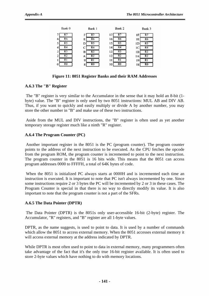
The 8051 Microcontroller Architecture
Appendix-A
Figure 11: 8051 Register Banks and their RAM Addresses
A.6.3 The "B" Register
The "B" register is very similar to the Accumulator in the sense that it may hold an 8-bit (1-byte) value. The "B" register is only used by two 8051 instructions: MUL AB and DIV AB. Thus, if you want to quickly and easily multiply or divide A by another number, you may store the other number in "B" and make use of these two instructions.
Aside from the MUL and DIV instructions, the "B" register is often used as yet another temporary storage register much like a ninth "R" register.
A.6.4 The Program Counter (PC)
Another important register in the 8051 is the PC (program counter). The program counter points to the address of the next instruction to be executed. As the CPU fetches the opcode from the program ROM, the program counter is incremented to point to the next instruction. The program counter in the 8051 is 16 bits wide. This means that the 8051 can access program addresses 0000 to FFFFH, a total of 64K bytes of code.
When the 8051 is initialized PC always starts at 0000H and is incremented each time an instruction is executed. It is important to note that PC isn't always incremented by one. Since some instructions require 2 or 3 bytes the PC will be incremented by 2 or 3 in these cases. The Program Counter is special in that there is no way to directly modify its value. It is also important to note that the program counter is not a part of the SFRs.
A.6.5 The Data Pointer (DPTR)
The Data Pointer (DPTR) is the 8051s only user-accessible 16-bit (2-byte) register. The Accumulator, "R" registers, and "B" register are all 1-byte values.
DPTR, as the name suggests, is used to point to data. It is used by a number of commands which allow the 8051 to access external memory. When the 8051 accesses external memory it will access external memory at the address indicated by DPTR.
While DPTR is most often used to point to data in external memory, many programmers often take advantage of the fact that it's the only true 16-bit register available. It is often used to store 2-byte values which have nothing to do with memory locations.
- 141 -

The 8051 Microcontroller Architecture
Appendix-A
A.6.6 The Stack Pointer (SP)
The stack is a section of RAM used by the CPU to store information temporarily. This information could be data or an address. The CPU needs this storage area since there are only a limited number of registers. The register used to access the stack is called the SP (stack pointer) register. The Stack Pointer, like all registers except DPTR and PC, may hold an 8-bit (1-byte) value. The Stack Pointer is used to indicate where the next value to be removed from the stack should be taken from. When pushing a value onto the stack, the 8051 first increments the value of SP and then stores the value at the resulting memory location. When popping a value off the stack, the 8051 returns the value from the memory location indicated by SP, and then decrements the value of SP.
When the 8051 is powered up, the SP register contains the value 07. This means that RAM location 08 is the first location used for the stack by the 8051. Locations 08 to 1F in the 8051 RAM can be used for the stack. This is because locations 20 – 2FH of RAM are reserved for bit-addressable memory and must not be used by the stack. If in a given program we need more than 24 bytes (08 to 1FH = 24 bytes) of stack, we can change the SP to point to RAM locations 30 – 7FH. This is done with the instruction “MOV SP, #2FH”.
Also, there is a problem with the default setting of the stack. Since SP = 07 when the 8051 is powered up, the first location of the stack is RAM location 08, which also belongs to register R0 of register bank 1. In other words, register bank 1 and the stack are using the same memory space. If in a given program we need to use register banks 1 and 2, we can reallocate another section of RAM to the stack. The general purpose RAM starting at address 30H is a good spot to place the stack. To do so we need to change the contents of the SP to 2FH.
A.6.7 The Program Status Word (PSW) Register The program status word (PSW) register is an 8-bit register. It is also referred to as the flag register. The PSW is at location D0H and is bit addressable. Although the PSW register is 8 bits wide, only 6 bits of it are used by the 8051. The two unused bits are user-definable flags. Four of the flags are called conditional flags, meaning that they indicate some conditions that result after an instruction is executed. These four are C (carry), AC (auxiliary carry), P (parity), and OV (overflow). As seen from Figure 12, the bits PSW.3 and PSW.4 are designated as RS0 and RS1, respectively, and are used to select a certain register bank. The PSW.5 and PSW.1 bits are general-purpose status flag bits and can be used by the programmer for any purpose. In other words, they are user definable.
- 142 -
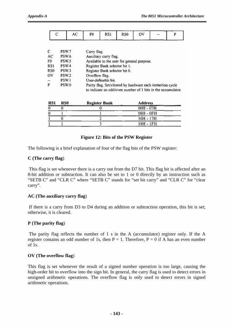
The 8051 Microcontroller Architecture
Appendix-A
Figure 12: Bits of the PSW Register
The following is a brief explanation of four of the flag bits of the PSW register:
C (The carry flag) This flag is set whenever there is a carry out from the D7 bit. This flag bit is affected after an 8-bit addition or subtraction. It can also be set to 1 or 0 directly by an instruction such as “SETB C” and “CLR C” where “SETB C” stands for “set bit carry” and “CLR C” for “clear carry”. AC (The auxiliary carry flag) If there is a carry from D3 to D4 during an addition or subtraction operation, this bit is set; otherwise, it is cleared. P (The parity flag) The parity flag reflects the number of 1 s in the A (accumulator) register only. If the A register contains an odd number of 1s, then P = 1. Therefore, P = 0 if A has an even number of 1s. OV (The overflow flag) This flag is set whenever the result of a signed number operation is too large, causing the high-order bit to overflow into the sign bit. In general, the carry flag is used to detect errors in unsigned arithmetic operations. The overflow flag is only used to detect errors in signed arithmetic operations.
- 143 -

The 8051 Microcontroller Architecture
Appendix-A
A.7 The 8051 I/O Ports The four ports P0, P1, P2, and P3 each use 8 pins, making them 8-bit ports. All the ports upon RESET are configured as inputs, ready to be used as input ports. When the first 0 is written to a port, it becomes an output. To reconfigure it as an input, a 1 must be sent to the port. Port 0 Port 0 occupies a total of 8 pins (pins 32 -39). It can be used for input or output. To use the pins of port 0 as both input and output ports, each pin must be connected externally to a l0K-ohm pull-up resistor. This is due to the fact that P0 is an open drain, unlike P1, P2, and P3, as we will see soon. Open drain is a term used for MOS chips in the same way that open collector is used for TTL chips. In any system using the 8051/52 chip, we normally connect P0 to pull-up resistors as shown in Figure 13. In this way we take advantage of port 0 for both input and output.
Figure 13: Port 0 with Pull-Up Resistors
As shown in Figure 14, port 0 is also designated as AD0 – AD7, allowing it to be used for both address and data. When connecting an 8051/31 to an external memory, port 0 provides both address and data. The 8051 multiplexes address and data through port 0 to save pins. Port 1 Port 1 occupies a total of 8 pins (pins 1 through 8). It can be used as input or output. In contrast to port 0, this port does not need any pull-up resistors since it already has pull-up resistors internally. Upon reset, port 1 is configured as an input port. Port 2 Port 2 occupies a total of 8 pins (pins 21 through 28). It can be used as input or output. Just like P1, port 2 does not need any pull-up resistors since it already has pull-up resistors internally. Upon reset, port 2 is configured as an input port. In many systems based on the 8051, P2 is used as simple I/O. However, in 8031-based systems, port 2 must be used along with P0 to provide the 16-bit address for external memory.
- 144 -

The 8051 Microcontroller Architecture
Appendix-A
Figure 14: The 8051 Pin Configuration with Alternative Pin Functions
As shown in Figure 14, port 2 is also designated as A8 – A15, indicating its dual function. Since an 8051/31 is capable of accessing 64K bytes of external memory, it needs a path for the 16 bits of the address. While P0 provides the lower 8 bits via A0 – A7, it is the job of P2 to provide bits A8 -A15 of the address. In other words, when the 8051/31 is connected to external memory, P2 is used for the upper 8 bits of the 16-bit address, and it cannot be used for I/O. Port 3 Port 3 occupies a total of 8 pins, pins 10 through 17. It can be used as input or output. P3 does not need any pull-up resistors, just as P1 and P2 did not. Although port 3 is configured as an input port upon reset, this is not the way it is most commonly used. Port 3 has the additional function of providing some extremely important signals such as interrupts. Table-2 provides these alternate functions of P3. This information applies to both 8051 and 8031 chips.
Table-2: Port 3 Alternate Functions
- 145 -

The 8051 Microcontroller Architecture
Appendix-A
A.8 Exercises
1. What is the main difference between a microcontroller and a general purpose microprocessor?
2. What is meant by an embedded system? Give examples of such a system? 3. State the major difference between the 8051 and the 8031 microcontrollers? 4. What is the size of the on-chip ROM and internal RAM of the 8752 microcontroller? 5. What is the RAM address space of memory Bank 3? 6. If the crystal frequency of an 87C52 microcontroller chip is 22.1184 MHz, determine
the machine cycle, and the time required to execute three instructions, each taking one machine cycle.
7. Sketch a block diagram for an 8031 microcontroller chip connected to an external EPROM of (64K × 8 bits) organization.
8. What is the function of the ALE pin in the 8051 microcontroller? 9. Show what is the difference between connecting the EA pin to power supply VCC and
to ground? 10. Sketch a practical 8051 microcontroller circuit used to drive four LEDs with active
high inputs connected to port 0. 11. How many pins are associated to the 4 I/O ports? 12. What are the two 16-bit registers in the 8051? 13. What is the content of the stack pointer after RESET of the 8051? 14. Which bits of the PSW are responsible for selection of the register banks? 15. On power up, which of the register banks is used? 16. What is the address and size of the accumulator in the 8051 microcontroller? 17. A given 8051 microcontroller has 7FFFH as the address of its last location of on-chip
ROM. What is the size of the on-chip ROM for this IC? 18. What is the number of address lines and data lines in the 8051? 19. What are the ports which are used for external memory access? 20. What is the address space of the SFR registers? 21. What do we mean by the bit addressable RAM of the 8051?
- 146 -

Appendix-B The MIDE-51 Tutorial
Appendix-B
The MIDE-51 Tutorial
The M-IDE51 Studio for 8051 microcontrollers is the primary means for performing the compilation process for the 8051 microcontroller devices in order to generate the required Intel hex files. The M-IDE Studio for MCS-51 has a comprehensive set of features that allows you to edit, compile, and debug a file.
The M-IDE Studio for MCS-51 also allows you to write an 8051 source file with C programming language in addition to Assembly language. Using this software, you can see the errors by viewing report in the LST file. In fact the assembly file format for this software is compatible with that of the ASEM-51 assembler, and the C file is compatible with that of the SDCC compiler.
Figure 1: M-IDE Studio for MCS-51
You will notice that most of the toolbar buttons and menu options are disabled. This is because a file has not been created. To create a file, do the following:
B.1 Creating a New File
In order to create a new file, click on File menu or the new file icon as shown in Figure 1. After starting a new file, you'll see the page looking similar to that in Figure 2.
- 147 -

Appendix-B The MIDE-51 Tutorial
Figure 2: A Blank New File
B.2 Writing a Program
In order to implement the desired program, you may write the assembly program in a blank file. After writing the program, you will observe that there are no colors in the page. In this case you must save the program with the (*.asm) extension as shown in Figure 3.
Figure 3: Writing a Program
B.3 Saving Files
Save your file with an extension according to your program. In this case if your program is written in assembly language then you must save the file with the extension *.asm as shown in Figure 3.
Figure 3: Save as dialog
- 148 -

Appendix-B The MIDE-51 Tutorial
After saving the program you will see the file appearing with colors. This indicates that the instruction mnemonics are right reserved as shown in Figure 4
Figure 4: Mnemonics of instructions
B.4 Compiling Source Files
To load the file into your device, you need to compile the file *.asm to convert it into hex file. To compile the *.asm file into the *.hex file you can click the Build shortcut as shown in Figure 4.
B.5 Troubleshooting Errors
Assembly errors apply to the consistency of the assembly language program in syntax and semantics. If one of these errors is detected, it is flagged in the list file, and program execution continues.
Figure 5: No Error Messages
B.6 File Error Example
As seen in Figure 6, we have an instruction error with the S JMP mnemonic that should be SJMP. After detecting and correcting the error you must save the file and compile it again.
Figure 6: A File with Error
- 149 -

Appendix-B The MIDE-51 Tutorial
Figure 7: Error Massage Output Window
B.7 The LST File
If you like to see more details about the errors in your source file, you should see the *.LST file as depicted in the dialog box of Figures 8 and the LST file content in Figure 9.
Figure 8: Opening the LST file
Figure 9: LST file
- 150 -

Appendix-C MCU 8051 IDE Tutorial
Appendix-C
MCU 8051 IDE Tutorial MCU 8051 IDE Software is an integrated development environment for 8051 based microcontrollers and is intended for 8051 Assembly and C programming languages. It provides a simple graphical user interface (GUI) environment for editing Assembly and C source files, generating the required hex files, and running and simulating the programs. This tutorial gives you a quick start to the MCU 8051 IDE software for writing and running 8051 Assembly files. The user can log to the program’s help for more detailed information about this package. C.1 Starting the MCU 8051 IDE The program can be started from the Programs menu as shown in Fig.1.
Figure 1: Starting MCU 8051 IDE Software
After logging into the program, the start-up window of the software appears as shown in Fig.2.
- 151 -

Appendix-C MCU 8051 IDE Tutorial
Figure 2: Start-up Window for the MCU 8051 IDE Package C.2 Creating New Projects Before creating a new project, the user should first make a folder to save his project files. For example, the name 8051_Projects on the root directory of the hard disk (C :) is a suitable one. Projects are stored in XML (eXtensible Markup Language) files with extension .mcu8051ide. The MCU 8051 IDE's project is a set of some files in some directory (the project directory). And this along with the file with extension .mcu8051ide forms the project. To create a new project, go to the Project menu on the menu bar and then select New as shown in Fig.3.
- 152 -

Appendix-C MCU 8051 IDE Tutorial
Figure 3: Creating a New Project Once selecting a new project, a project creation dialogue appears as shown in Fig.4.
Figure 4: Project Creation Dialogue
From the dialogue window of Fig.4, you should give the project name (Test_Programs in this case), and select the project directory in which the project files will be stored (8051_Projects in this example). Furthermore, you should select the specific processor (microcontroller) for your project, and enable or disable the external RAM and ROM
- 153 -

Appendix-C MCU 8051 IDE Tutorial
memories. When enabling the external data and code memories, you must specify the memory space for each type. Fig.5 shows the MCU 8051 IDE environment after starting a new project.
Figure 5: The MCU 8051 IDE Environment C.3 Creating a New Source Code File Once you have created a new project you can begin to develop your code for your chosen processor. The code editor of the MCU 8051 IDE package is featured with syntax highlighting and validation, auto-completion and spell checking for comments, as well as a command line that speeds up the access to various editor options. It also provides a panel showing line numbers, bookmarks, breakpoints and warnings from syntax errors. In this example, the 8051 assembly file we wish to assemble and run is shown in Fig.6.
Figure 6: The source code file to be run by the 8051 simulator
- 154 -

Appendix-C MCU 8051 IDE Tutorial
The 8051 assembly file can be entered with the aid of the code editor as shown in Fig.7.
Figure 7: Writing and Editing the Assembly Source Code File C.4 Saving the Source Code File When you want to save your code press Ctrl+Shift+S, or select the Save as command from the File menu as shown in Fig.8.
Figure 8: Saving the Source Code File
- 155 -

Appendix-C MCU 8051 IDE Tutorial
After selecting the Save as command, the Save File window appears as shown in Fig.9. In this window, the file name and type should be entered. For this example, the file name is p1, while its extension is .asm (Assembly Language File).
Figure 9: The Save File Window After pressing the OK button, a dialogue box appears to confirm adding the recently saved assembly file (p1.asm) into the project directory as shown in Fig.10.
Figure 10: The Add File Dialogue Box
C.5 Compiling the Saved Source File In order to test the written assembly file and generate the required machine code (.hex) file, select the command Compile from the Tools menu as depicted in Fig.11. When starting the compilation process, we are actually running the Assembler of the MCU 8051IDE system. This Assembler is compatible with the ASEM51 Assembler.
- 156 -

Appendix-C MCU 8051 IDE Tutorial
Figure 11: Starting the Compilation of the Source File
The MCU 8051 IDE Assembler is capable of generating four kinds of output files:
1- Object code file (Machine code file) as a hexadecimal file with .hex extension.
2- Object code file (Machine code file) as a binary file with .bin extension.
3- List file with .lst extension.
4- Code file for integrated MCU simulator with .atf extension.
The compilation process for the written 8051 assembly file is shown in Fig.12. As shown from this figure, if the compilation process is successful then the generated files are presented in the bottom panel of the simulator window.
- 157 -

Appendix-C MCU 8051 IDE Tutorial
Figure 12: Compiling an 8051 Assembly File
C.6 Starting the Simulator The simulator of the MCU 8051 IDE package is a software component intended for the simulation of the chosen microcontroller in a virtual environment. It allows the user to monitor precisely what is happening in the microcontroller in an exact moment in time, as well as to modify its components, for instance by altering the value of a register, canceling an interrupt or forcing a subprogram to return. To start the simulator, select the command Start/Shutdown from the Simulator menu as shown in Fig.13. The Run command of the Simulator menu is used to execute the program as depicted in Fig.14.
- 158 -

Appendix-C MCU 8051 IDE Tutorial
Figure 13: Starting the MCU 8051 IDE Simulator
Figure 14: Running the Simulator
The result of the simulation process is presented at the bottom panel of the simulator window as shown in Fig.15.
- 159 -

Appendix-C MCU 8051 IDE Tutorial
Figure 15: Result of the Simulation Process This panel is the main part of the simulator user interface. It shows all microcontroller registers along with the content of internal data memory. It also contains small toolbar with 6 buttons: Start/ Shutdown, Reset, Step back, Step, Step over, Animate and Run. C.7 Step-by-Step Debugging Debugging is necessary to execute the program instructions individually. Step by step debugging can be performed by first selecting the command Debug this file only, and then the command step from the Simulator menu as shown in Fig.16 and Fig.17 respectively.
- 160 -

Appendix-C MCU 8051 IDE Tutorial
Figure 16: Debugger Starting
Figure 17: Step by Step Program Debugging
C.8 Viewing Memory Areas Different memory areas such as the SFR map, bit-accessible memory area, code memory area, stack, external RAM, and external ROM can be viewed from the Virtual MCU menu as shown in Fig.18.
- 161 -

Appendix-C MCU 8051 IDE Tutorial
Figure 18: Accessing Different Memory Areas
Figure 19: SFR Memory Area after Program Execution
- 162 -

Appendix-C MCU 8051 IDE Tutorial
Figure 20: Code Memory Area for the Program
C.9 Viewing the Machine Code File The generated machine code hexadecimal file (.hex file) can be accessed by opening it from the File menu or the Open file icon on the tools bar. This is indicated in Fig.21 and Fig.22 respectively.
Figure 21: Opening the hexadecimal file (p1.hex)
- 163 -
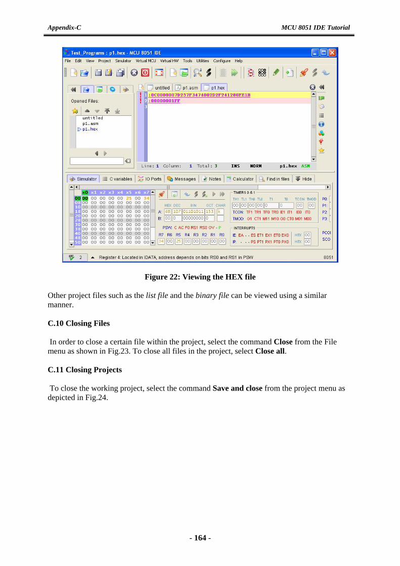
Appendix-C MCU 8051 IDE Tutorial
Figure 22: Viewing the HEX file Other project files such as the list file and the binary file can be viewed using a similar manner. C.10 Closing Files In order to close a certain file within the project, select the command Close from the File menu as shown in Fig.23. To close all files in the project, select Close all. C.11 Closing Projects To close the working project, select the command Save and close from the project menu as depicted in Fig.24.
- 164 -

Appendix-C MCU 8051 IDE Tutorial
Figure 23: Closing Files
Figure 24: Closing Projects
- 165 -

Appendix-C MCU 8051 IDE Tutorial
This page is left intentionally blank
- 166 -

Appendix-D Alphabetical List of the 8051 Instructions
Appendix-D
Alphabetical List of the 8051 Instructions
• ACALL - Absolute Call • ADD, ADDC - Add Accumulator (With Carry) • AJMP - Absolute Jump • ANL - Bitwise AND • CJNE - Compare and Jump if Not Equal • CLR - Clear Register • CPL - Complement Register • DA - Decimal Adjust • DEC - Decrement Register • DIV - Divide Accumulator by B • DJNZ - Decrement Register and Jump if Not Zero • INC - Increment Register • JB - Jump if Bit Set • JBC - Jump if Bit Set and Clear Bit • JC - Jump if Carry Set • JMP - Jump to Address • JNB - Jump if Bit Not Set • JNC - Jump if Carry Not Set • JNZ - Jump if Accumulator Not Zero • JZ - Jump if Accumulator Zero • LCALL - Long Call • LJMP - Long Jump • MOV - Move Memory • MOVC - Move Code Memory • MOVX - Move Extended Memory • MUL - Multiply Accumulator by B • NOP - No Operation • ORL - Bitwise OR • POP - Pop Value From Stack • PUSH - Push Value Onto Stack • RET - Return From Subroutine • RETI - Return From Interrupt • RL - Rotate Accumulator Left • RLC - Rotate Accumulator Left Through Carry • RR - Rotate Accumulator Right • RRC - Rotate Accumulator Right Through Carry • SETB - Set Bit • SJMP - Short Jump • SUBB - Subtract From Accumulator With Borrow • SWAP - Swap Accumulator Nibbles • XCH - Exchange Bytes • XCHD - Exchange Digits • XRL - Bitwise Exclusive OR
- 167 -

Appendix-D Alphabetical List of the 8051 Instructions
DATA TRANSFER INSTRUCTIONS
Mnemonic Description Bytes
MOV A,Rn Moves the register to the accumulator 1
MOV A,direct Moves the direct byte to the accumulator 2
MOV A,@Ri Moves the indirect RAM to the accumulator 1
MOV A,#data Moves the immediate data to the accumulator 2
MOV Rn,A Moves the accumulator to the register 1
MOV Rn,direct Moves the direct byte to the register 2
MOV Rn,#data Moves the immediate data to the register 2
MOV direct,A Moves the accumulator to the direct byte 2
MOV direct,Rn Moves the register to the direct byte 2
MOV direct,direct Moves the direct byte to the direct byte 3
MOV direct,@Ri Moves the indirect RAM to the direct byte 2
MOV direct,#data Moves the immediate data to the direct byte 3
MOV @Ri,A Moves the accumulator to the indirect RAM 1
MOV @Ri,direct Moves the direct byte to the indirect RAM 2
MOV @Ri,#data Moves the immediate data to the indirect RAM 2
MOV DPTR,#data Moves a 16-bit data to the data pointer 3
MOVC A,@A+DPTR Moves the code byte relative to the DPTR to the accumulator (address=A+DPTR) 1
MOVC A,@A+PC Moves the code byte relative to the PC to the accumulator (address=A+PC) 1
MOVX A,@Ri Moves the external RAM (8-bit address) to the accumulator 1
MOVX A,@DPTR Moves the external RAM (16-bit address) to the accumulator 1
MOVX @Ri,A Moves the accumulator to the external RAM (8-bit address) 1
MOVX @DPTR,A Moves the accumulator to the external RAM (16-bit address) 1
PUSH direct Pushes the direct byte onto the stack 2
POP direct Pops the direct byte from the stack/td> 2
XCH A,Rn Exchanges the register with the accumulator 1
XCH A,direct Exchanges the direct byte with the accumulator 2
XCH A,@Ri Exchanges the indirect RAM with the accumulator 1
XCHD A,@Ri Exchanges the low-order nibble indirect RAM with the accumulator 1
- 168 -

Appendix-D Alphabetical List of the 8051 Instructions
BRANCH INSTRUCTIONS
Mnemonic Description Bytes
ACALL addr11 Absolute subroutine call 2
LCALL addr16 Long subroutine call 3
RET Returns from subroutine 1
RETI Returns from interrupt subroutine 1
AJMP addr11 Absolute jump 2
LJMP addr16 Long jump 3
SJMP rel Short jump (from –128 to +127 locations relative to the following instruction) 2
JC rel Jump if carry flag is set. Short jump. 2
JNC rel Jump if carry flag is not set. Short jump. 2
JB bit,rel Jump if direct bit is set. Short jump. 3
JBC bit,rel Jump if direct bit is set and clears bit. Short jump. 3
JMP @A+DPTR Jump indirect relative to the DPTR 1
JZ rel Jump if the accumulator is zero. Short jump. 2
JNZ rel Jump if the accumulator is not zero. Short jump. 2
CJNE A,direct,rel Compares direct byte to the accumulator and jumps if not equal. Short jump. 3
CJNE A,#data,rel Compares immediate data to the accumulator and jumps if not equal. Short jump. 3
CJNE Rn,#data,rel Compares immediate data to the register and jumps if not equal. Short jump. 3
CJNE @Ri,#data,rel Compares immediate data to indirect register and jumps if not equal. Short jump. 3
DJNZ Rn,rel Decrements register and jumps if not 0. Short jump. 2
DJNZ Rx,rel Decrements direct byte and jump if not 0. Short jump. 3
NOP No operation 1
- 169 -

Appendix-D Alphabetical List of the 8051 Instructions
ARITHMETIC INSTRUCTIONS
Mnemonic Description Bytes
ADD A,Rn Adds the register to the accumulator 1
ADD A,direct Adds the direct byte to the accumulator 2
ADD A,@Ri Adds the indirect RAM to the accumulator 1
ADD A,#data Adds the immediate data to the accumulator 2
ADDC A,Rn Adds the register to the accumulator with a carry flag 1
ADDC A,direct Adds the direct byte to the accumulator with a carry flag 2
ADDC A,@Ri Adds the indirect RAM to the accumulator with a carry flag 1
ADDC A,#data Adds the immediate data to the accumulator with a carry flag 2
SUBB A,Rn Subtracts the register from the accumulator with a borrow 1
SUBB A,direct Subtracts the direct byte from the accumulator with a borrow 2
SUBB A,@Ri Subtracts the indirect RAM from the accumulator with a borrow 1
SUBB A,#data Subtracts the immediate data from the accumulator with a borrow 2
INC A Increments the accumulator by 1 1
INC Rn Increments the register by 1 1
INC Rx Increments the direct byte by 1 2
INC @Ri Increments the indirect RAM by 1 1
DEC A Decrements the accumulator by 1 1
DEC Rn Decrements the register by 1 1
DEC Rx Decrements the direct byte by 1 1
DEC @Ri Decrements the indirect RAM by 1 2
INC DPTR Increments the Data Pointer by 1 1
MUL AB Multiplies A and B 1
DIV AB Divides A by B 1
DA A Decimal adjustment of the accumulator according to BCD code 1
- 170 -
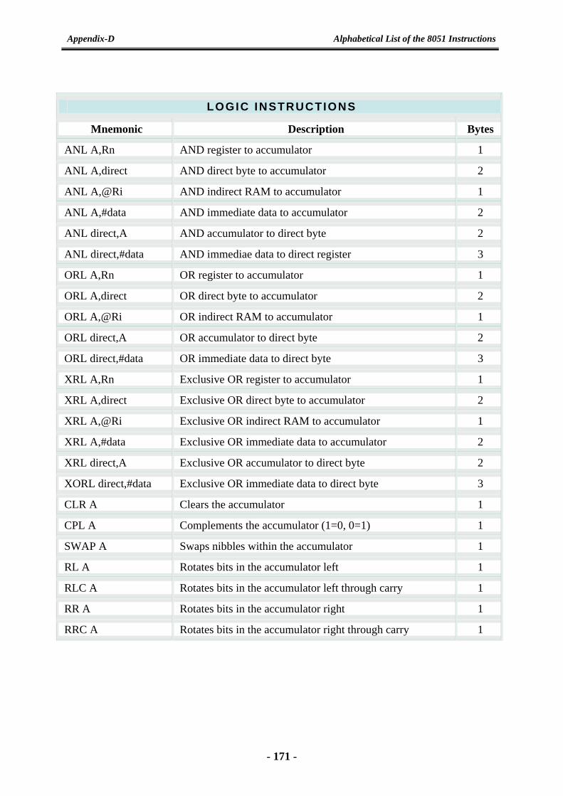
Appendix-D Alphabetical List of the 8051 Instructions
LOGIC INSTRUCTIONS
Mnemonic Description Bytes
ANL A,Rn AND register to accumulator 1
ANL A,direct AND direct byte to accumulator 2
ANL A,@Ri AND indirect RAM to accumulator 1
ANL A,#data AND immediate data to accumulator 2
ANL direct,A AND accumulator to direct byte 2
ANL direct,#data AND immediae data to direct register 3
ORL A,Rn OR register to accumulator 1
ORL A,direct OR direct byte to accumulator 2
ORL A,@Ri OR indirect RAM to accumulator 1
ORL direct,A OR accumulator to direct byte 2
ORL direct,#data OR immediate data to direct byte 3
XRL A,Rn Exclusive OR register to accumulator 1
XRL A,direct Exclusive OR direct byte to accumulator 2
XRL A,@Ri Exclusive OR indirect RAM to accumulator 1
XRL A,#data Exclusive OR immediate data to accumulator 2
XRL direct,A Exclusive OR accumulator to direct byte 2
XORL direct,#data Exclusive OR immediate data to direct byte 3
CLR A Clears the accumulator 1
CPL A Complements the accumulator (1=0, 0=1) 1
SWAP A Swaps nibbles within the accumulator 1
RL A Rotates bits in the accumulator left 1
RLC A Rotates bits in the accumulator left through carry 1
RR A Rotates bits in the accumulator right 1
RRC A Rotates bits in the accumulator right through carry 1
- 171 -