Equivalent Circuit Model for Current Mode Controls and … · Current-mode control architectures...
160
Equivalent Circuit Model for Current Mode Controls and Its Extensions Yingyi Yan Dissertation submitted to the Faculty of the Virginia Polytechnic Institute and State University in partial fulfillment of the requirements for the degree of Doctor of Philosophy in Electrical Engineering Fred C. Lee, Chair Paolo Mattavelli Qiang Li Jaime De La Reelopez Elaine P. Scott January 29 th , 2013 Blacksburg, Virginia Keywords: current-mode control, modeling, three-terminal switch model, equivalent circuit © 2013, Yingyi Yan
Transcript of Equivalent Circuit Model for Current Mode Controls and … · Current-mode control architectures...
Equivalent Circuit Model for Current Mode
Controls and Its Extensions
Yingyi Yan
Dissertation submitted to the Faculty of the
Virginia Polytechnic Institute and State University
in partial fulfillment of the requirements for the degree of
Doctor of Philosophy
in
Electrical Engineering
Fred C. Lee, Chair
Paolo Mattavelli
Qiang Li
Jaime De La Reelopez
Elaine P. Scott
January 29th
, 2013
Blacksburg, Virginia
Keywords: current-mode control, modeling,
three-terminal switch model, equivalent circuit
© 2013, Yingyi Yan

Equivalent Circuit Model for Current Mode
Controls and Its Extensions
Yingyi Yan
(Abstract)
Current-mode control architectures have been an indispensable technique in
many applications, such as Voltage Regulator, Point-of-load converters, power factor
correction, battery charger and LED driver. Since the inductor current ramp is used in
the modulator in current-mode control without any low pass filter, high order
harmonics play important role in the feedback control. This is the reason for the
difficulty in obtaining the small-signal model for current-mode control in the frequency
domain. A continuous time domain model was recently proposed as a successful model
for current-mode control architectures. However, the model was derived by describing
function method, which is very arithmatically complicated, not to mention time
consuming.
For the analysis and design of non-linear system, equivalent circuit model,
which is user friendly and intuitive, is an effective tool. In this dissertation, the
primary objective is to develop a unified three-terminal switch model for current-mode
controls using the results of describing function derivation, which characterizes the
small signal property of the common subcircuit of current mode controlled PWM
converters. Its application is extended to average current mode control, V2 control and
other proposed novel current mode control schemes.
First, the existing model for current mode control is reviewed. The limitations of
exsiting model for current-mode control are identified. Based on the universal small
signal relationship between terminal currents and the results of describing function
derivation, a unified three-terminal switch model for current mode control is proposed.
A three-terminal equivalent circuit is developed to represent the small signal behavior

iii
of this common sub-circuit. The proposed model is applicable in both constant
frequency and variable frequency modulation.
After that, the modeling of digital predictive current mode control is presented.
Predictive current mode control is one of the promising digital current mode control
method featuring fast dynamic response and low sample rate requirement. Many
implementations were presented in past ten years. To understand the benefit and the
limitation of each implementation, help the engineer to choose the modulation scheme
and design the control loop, a small signal Laplace-domain model for digital
predictive current mode controls is proposed. The model is extended to the
multi-sampled implementation. The modeling result is summarize as the small signal
equivalent circuit mode, whose form is consistant with that of analog current mode
controls. Based on S-domain model, digital predictive current mode controls are
compared with analog implementation to demonstrate the advantages and limitation.
Implementation selection guideline and compensation is discussed based on the
modeling results.
Then, using the proposed unified model is used in the analysis of average current
mode control. Under proper design, the inductor current ripple passes through the
current compensator and appears in PWM comparator. It significantly influence the
high frequency small signal property of the converter. In chapter 3, the proportional
feedback is separated from integral feedback so that the sideband frequency feedback
effect can be taken into consideration. It extends the results obtained in peak-current
model control to average current mode control. The proposed small signal model is
accurate up to half switching frequency, predicting the sub-harmonic instability.
Based on the proposed model, a new feedback design guideline is proposed. By
designing the external ramp following the proposed design guideline, quality factor of
the double poles at half of switching frequency in control-to-output transfer function
can be precisely controlled. This helps the feedback design to achieve widest control
bandwidth and proper damping.

iv
V2 control is a popular control scheme in Point-of-load converters due to the
unique fast transient response. As the output voltage ripple is used as PWM
modulation ramp, V2 control has close relationship with current mode control but this
relationship was not addressed in the exsiting model. Chapter 4 utilizes the
three-terminal switch model to build the equivalent circuit model for V2 control,
which clearly shows that V2 control is a particular implementation of current mode
control, with proportional capacitor voltage feedback and load current feedback
embeded.
The analysis presented in Chapter 3 provides a clear physical understanding of
average current mode control. With constant frequency modulation, the control
bandwidth is usually limited by the double pole at half of swithcing frequency,
especially in the converters with wide duty cycle range. Chapter 5 proposed a novel I2
current mode control to improve the dynamic performance of average current mode
control. In particular, constant on-time I2 control eliminates the need of external ramp
while the current loop is inherently stable. Moreover, constant on-time modulation
improves the light load efficiency.
As a conclusion, this dissertation proposed a unified three-terminal switch model
for current mode controls. The application of this equivalent circuit model is extended
to average current mode control, V2 control and the novel I
2 current mode control. The
Laplace-domain model of predictive current mode control is also presented. All the
modeling results are verified through simulation and experiments.

v
Acknowledgments
For their support and direction over years, I would like to express my heartfelt
gratitude to all my professors at Virginia Tech, without whom my research and this
thesis would not have been possible. In particular, I am very grateful to my advisor
and committee chair, Professor Fred C. Lee, his kind help not only with research but
also with my life at Virginia Tech. He is always generous to give me suggestions and
ideas to help me focus on some unknown areas. His logical thoughts and earnest
attitude gave me courage when I met problems. He often shares his philosophy with
me, which is the most beneficial to me. His help has become my life-long heritage. I
would also like to give specific appreciation to Professor Paolo Mattavelli, whose
teaching, support, and critical insights influenced me in many ways. I have learned a
lot from him. Dr. Mattavelli’s rich knowledge and suggestions inspires me a lot. Both
of them have a great impact on my life and my future career. I also wish to thank the
other members of my advisory committee, Dr. Qiang Li, Dr. Jaime De La Ree , and
Dr. Elaine P. Scott, for their support, suggestions and encouragement throughout this
entire process.
I am especially indebted to my colleagues in the VRM Group and Digital
Control Group. In particular, I would like to thank Dr. Jian Li for his help and time on
my research. It has been a great pleasure to work with the talented, creative, helpful
and dedicated colleagues. I would like to thank all the members of our teams: Dr.
Authur Ball, Dr. Shuo Wang, Dr. Ching Jan Chen, Dr. Feng Zheng, Mr. Clark Person,
Mr. Chanwit Prasantanakorn, Dr. Chuanyun Wang, Dr. Dianbo Fu, Dr. Yan Jiang, Mr.
Doug Sterk, Dr. David Reusch, Mr. Zheng Luo, Dr. Fanghua Zhang, Dr. Yuling Li,
Dr. Shaojun Xie, Mr. Weiyi Feng, Dr. Ke Jin, Dr. Brian Cheng, Dr. Xiaoyong Ren, Dr.
Yan Dong, Mr. Zhiqiang Wang, Mr. Haoran Wu, Mr. Mingkai Mu, Mr. Yi Sun, Dr.
Pengju Kong, Mr. Yipeng Su, Mr. Daocheng Huang, Dr. Qiang Li, Mr. Wei Zhang,
Mr. Pengjie Lai, Mr. Zijian Wang, Mr. Qian Li, Mr. Feng Yu, Mr. Li Jiang and Mr.
Shuilin Tian, Mr. Pei-Hsin Liu, Mr. Yuchen Yang, Mr. Xiucheng Huang, Mr. Yang

vi
Jiao, Mr. Zhengyang Liu. My thanks also go to all of the other students I have met
in CPES, especially to Mr. Jing Xue, Ms. Zhuxian Xu, Mr.Yin Wang, Ms. Ying Lu,
Dr. Michele Lim, Dr. Rixin Lai, Dr. Honggang Sheng, Dr. Dong Dong, Dr. Di Zhang,
Dr. Puqi Ning, Dr. Zheng Zhao, Dr. Ruxi Wang and Dr. Dong Jiang. It has been a
great pleasure, and I’ve had fun with them.
I would also like to give special mention to the wonderful members of the CPES
staff who were always willing to help me out, Ms. Teresa Shaw, Ms. Linda Gallagher,
Ms. Teresa Rose, Ms. Marianne Hawthorne, Ms. Linda Long, Mr. Robert Martin, Mr.
Doug Sterk, Mr. Jamie Evans, Mr. Dan Huff, and Mr. David Fuller. Moreover, I owe
a debt of the deepest gratitude to Ms. Suzanne Farmer, who offered me a great help in
polishing my writing.
My deepest appreciation goes toward my parents, and my parents-in-law, who
have always provided support and encouragement throughout my further education.
Last but not least, with deepest love, I dedicate my appreciation to my wife, who
has always been there with her love, support, understanding and encouragement for
all my endeavors. Your love and encouragement has been the most valuable thing in
my life!

vii
This work was supported by the power management consortium (Chicony
Power, Delta Electronics, Huawei Technologies, Infineon Technologies, International
Rectifier, Linear Technology, Lite-On Technology, Murata Manufacturing Co., Ltd.,
NEC TOKIN Corporation, NXP Semiconductors, Richtek Technology, Texas
Instruments, ZTE Corporation), and the Engineering Research Center Shared Facilities
supported by the National Science Foundation under NSF Award Number
EEC-9731677. Any opinions, findings and conclusions or recommendations
expressed in this material are those of the author and do not necessarily reflect those
of the National Science Foundation.
This work was conducted with the use of SIMPLIS software, donated in kind by
Simplis Technology of the CPES Industrial Consortium.

viii
Table of Contents
Chapter 1. Introduction ................................................................................................................... 1
1.1 Research Background: Current-Mode Control ..................................................................... 1
1.2 Applications of Current-Mode Control .................................................................................. 3
1.3 Existing Models for Current Mode Controls with Proportional Current Feedback ........ 14
1.4 Existing Models for Other Current Mode Controls ............................................................ 25
1.5 Dissertation Outline ................................................................................................................ 29
Chapter 2. Unified Three-Terminal Switch Model for Current Mode Controls ...................... 32
2.1 Common Invariant Structure in Current Mode Control Power Converters .................... 32
2.2 General Small Signal Relationship for Three-terminal Switch .......................................... 34
2.3 Three-terminal Switch Model for Peak Current Mode Control ........................................ 37
2.4 Discussion on Physical Meaning of Three-Terminal Switch Model ................................... 43
2.5 Model Extension to Other Current Mode Controls ............................................................. 45
2.6 Three-Terminal Switch Model for Digital Predictive Current Mode Controls ................ 47
2.7 Verification of the Proposed Model ...................................................................................... 65
2.8 Summary ................................................................................................................................. 70
Chapter 3. Extend Equivalent Circuit to Average Current Mode Control and Design
Guideline 72
3.1 Introduction ............................................................................................................................ 72
3.2 Proposed Model for Average Current Mode Control ......................................................... 75
3.3 Analysis of the Small Signal Model and Design Guideline .................................................. 78
3.4 Model Extension to Other Modulations ................................................................................ 86
3.5 The Analysis of Other Converters with Average Current Mode Control ......................... 87

ix
3.6 Simulation and Experimental Verification ........................................................................... 87
3.7 Conclusion ............................................................................................................................... 90
Chapter 4. The Extension of Equivalent Circuit to V2 Control .................................................. 91
4.1 Introduction ............................................................................................................................ 91
4.2 Small Signal Model Equivalent Circuit for V2 Control and Analysis ................................ 94
4.3 Model Extension to Constant Frequency V2 Control ........................................................ 103
4.4 Equivalent Circuit Model for Enhanced V2 Control and Analysis .................................. 104
4.5 Simulation and Experimental Verification ......................................................................... 107
4.6 Summary ............................................................................................................................... 110
Chapter 5. I2 Current Mode Control for Switching Converters .............................................. 111
5.1 Introduction .......................................................................................................................... 111
5.2 Review of Peak Current Mode Control and Average Current Mode Control ................ 112
5.3 Proposed I2 Average Current Mode Control ..................................................................... 118
5.4 Small Signal Model and Design Guideline ......................................................................... 121
5.5 Concept Extensions............................................................................................................... 124
5.6 Simulation and Experimental Results ................................................................................. 127
5.7 Summary ............................................................................................................................... 130
Chapter 6. Conclusions and Future Work ................................................................................. 131
6.1 Summary ............................................................................................................................... 131
6.2 Future Work ......................................................................................................................... 133
Reference ............................................................................................................................................. 134

x
List of Tables
Table 2.1. Parameters Definition of Equivalent Circuit (Figure 2.7) .................... 39
Table 2.2. Parameters Definition of Three-terminal Switch Model (Figure 2.12) 46
Table 2.3. Quality factor of double poles and delay time ..................................... 58
Table 2.4. Delay time of each modulation law with N samples/Tsw ..................... 59
Table 2.5. Definition of Re, Ce and Tdelay for digital predictive current mode
controls .......................................................................................................... 64

xi
List of Figures
Figure 1.1 Control structure of Current-mode control ............................................ 1
Figure 1.2 Different modulation schemes in current-mode control: (a) peak
current-mode control, (b) valley current mode control, (c) constant on-time
control, (d) constant off-time control, (e) charge control and (f)average
current mode control ....................................................................................... 2
Figure 1.3. Average current mode controlled Buck converter ................................ 3
Figure 1.4 Architecture of V2 Control ..................................................................... 3
Figure 1.5 A typical distributed power system ........................................................ 4
Figure 1.6 A multi-phase buck converter with peak current-mode control ............. 5
Figure 1.7 Output impedance specification of Intel VRD 11.1 ............................... 6
Figure 1.8 Constant On-time V2 Control ................................................................ 7
Figure 1.9 Constant On-time V2 Control without outer loop .................................. 7
Figure 1.10 Average current mode controlled CCM Boost PFC ............................. 8
Figure 1.11 Constant off-time current mode control CCM Boost PFC .................. 9
Figure 1.12 Charge control Flyback PFC .............................................................. 10
Figure 1.13 Typical charge current and voltage profile ........................................ 11
Figure 1.14 Bi-directional Flyback charger and DC/DC converter ...................... 12
Figure 1.15 Current mode control Buck LED driver ............................................ 14
Figure 1.16 current-mode control: (a) control structure, (b) “current source”
concept .......................................................................................................... 16
Figure 1.17 Average model for current-mode control with two additional feed
forward gain and feedback gain .................................................................... 17
Figure 1.18 Control-to-output transfer function comparison (D=0.45) ................ 18
Figure 1.19 Discrete-time analysis: (a) natural response, and (b) forced response
....................................................................................................................... 18
Figure 1.20. R. Ridley’ model for peak current-mode control .............................. 21
Figure 1.21 Control-to-output transfer function based on R. Ridley’ model (se = 0)
....................................................................................................................... 21
xii
Figure 1.22. F. D. Tan and R. D. Middlebrook’s model for peak current-mode
control ............................................................................................................ 22
Figure 1.23. Perturbed inductor current waveform: (a) in peak current-mode
control, and (b) in constant on-time control ............................................... 23
Figure 1.24. Discrepancy in the extended model .................................................. 23
Figure 1.25. Perturbed inductor current waveform in peak current-mode control 24
Figure 1.26. Equivalent circuit for current mode control Buck converter ............ 25
Figure 1.27. Average model for Average current mode control ............................ 26
Figure 1.28. Modified average model for average current model control ............ 27
Figure 1.29 Model for V2 Control based on modified average model of current
mode control .................................................................................................. 28
Figure 1.30 Modeling of V2 control based on describing function ....................... 28
Figure 1.31 Equivalent circuit model in [C10] of V2 control ................................ 29
Figure 2.1. Current mode control DC/DC converters ........................................... 33
Figure 2.2. Common invariant structure in current mode control power converters
....................................................................................................................... 34
Figure 2.3. Basic waveform of PWM switch ........................................................ 35
Figure 2.4. Duty cycle to switch current transfer function (fixed frequency
modulation) ................................................................................................... 36
Figure 2.5. Duty cycle to switch current transfer function(variable frequency
modulation) ................................................................................................... 37
Figure 2.6. Current mode control Buck converter ................................................ 38
Figure 2.7. Equivalent circuit for current mode control Buck converter .............. 39
Figure 2.8. Equivalent circuit with DC transformer .............................................. 41
Figure 2.9. Complete equivalent circuit for peak current mode control Buck
converter ........................................................................................................ 43
Figure 2.10. Three terminal equivalent circuit model for peak current mode
control ............................................................................................................ 43
Figure 2.11. Three terminal equivalent circuit model degenerates to three-terminal
xiii
switch mode for the power stage when se>>sn,sf ........................................... 45
Figure 2.12. Unified three terminal equivalent circuit model for current mode
controls .......................................................................................................... 46
Figure 2.13 Predictive Current Control Buck Converter ...................................... 49
Figure 2.14. Asymmetrical double edge valley current mode control .................. 50
Figure 2.15. Perturbed inductor current waveform ............................................... 53
Figure 2.16. Transfer Function iL(s)/vc(s) (D=0.1) ................................................ 55
Figure 2.17. Simulation verification for vo*(s)/vc*(s) of Buck ( fsw=300kHz,
Vin=12V, Vo=5V, Ls=300nH, Co=4800μF, RCo=0.75mΩ, RL=0.1Ω, 4
sample/cycle) ................................................................................................. 61
Figure 2.18. Common sub-circuit of predictive current mode controlled
converters ...................................................................................................... 62
Figure 2.19. Unified three-terminal switch equivalent circuit model for predictive
current mode control ..................................................................................... 62
Figure 2.20. Equivalent circuit for predictive current mode control Buck converter
....................................................................................................................... 65
Figure 2.21. Simulation verification of control-to-output and input-to-output
transfer function for peak current mode control Buck converter .................. 66
Figure 2.22. Simulation verification of output impedance and input impedance for
peak current mode control Buck converter ................................................... 66
Figure 2.23. Peak current mode control Boost converter and its small signal
equivalent circuit ........................................................................................... 67
Figure 2.24. Simulation verification of control-to-output and input-to-output
transfer function for peak current mode control Boost converter ................. 67
Figure 2.25. Simulation verification of output impedance and input impedance for
peak current mode control Boost converter .................................................. 68
Figure 2.26. Charge controlled Flyback converter and its small signal equivalent
circuit ............................................................................................................. 69
Figure 2.27. Simulation verification of control-to-input current and
xiv
control-to-output transfer function for charge control Flyback converter .... 69
Figure 2.28. Simulation verification of control-to-output and input-to-output
transfer function for constant on-time current mode control Buck converter
....................................................................................................................... 70
Figure 2.29. Simulation verification of input impedance and output impedance for
constant on-time current mode control Buck converter ................................ 71
Figure 3.1. Average current mode controlled Buck converter .............................. 73
Figure 3.2. Control-to-iL transfer function comparison (Vin=12V, Vo=5V,
Ls=300nH, Co=3mF, Rz=20kΩ, RA=1kΩ, Cz=100nF, RL=0.5Ω, se=2V) ...... 74
Figure 3.3. Separation of current feedback information ....................................... 77
Figure 3.4. Comparison of the gain of integration and proportional term ............ 77
Figure 3.5. Small signal equivalent circuit for average current mode control ...... 78
Figure 3.6. Control-to-iL transfer function comparison (Vin=12V, Vo=5V,
Ls=300nH, Co=3mF, Rz=2kΩ, RA=1kΩ, Cz=1μF, RL=0.5Ω, se=0.2V) ......... 78
Figure 3.7. Transition between average current mode control and peak current
mode control .................................................................................................. 81
Figure 3.8. Comparison of control-to-output transfer function with different
external ramp compensation .......................................................................... 82
Figure 3.9. Design example of average current mode control .............................. 84
Figure 3.10. Simulation waveform for load transient response ............................ 84
Figure 3.11. Comparison of conventional design and proposed design ................ 85
Figure 3.12. Average current mode controlled Buck converter with
Trans-conductance amplifier ......................................................................... 86
Figure 3.13. Average current mode controlled Boost converter and its small signal
equivalent circuit ........................................................................................... 88
Figure 3.14. Control-to-iL and control-to-output transfer function comparison ... 89
Figure 3.15. Control-to-iL and control-to-output transfer function comparison ... 89
Figure 4.1 Constant On-time V2 Control .............................................................. 92
Figure 4.2 Describing function model in large external ramp case....................... 93

xv
Figure 4.3 Model for output impedance in [C10] ................................................. 94
Figure 4.4 V2 Control with explicit three feedbacks ........................................... 95
Figure 4.5 Impedance comparison between RL and output capacitor ................... 97
Figure 4.6 Impedance comparison between output capacitor ESR and capacitance
....................................................................................................................... 97
Figure 4.7 Small signal equivalent Circuit of V2 Control ..................................... 98
Figure 4.8 The effect of each loop on vo(s)/vc(s) .................................................. 98
Figure 4.9 Capacitor voltage loop gain ................................................................. 99
Figure 4.10 The effect of each loop on output impedance .................................. 100
Figure 4.11 Audio susceptibility of constant on-time V2 Control ....................... 102
Figure 4.12 Input impedance of constant on-time V2 Control ............................ 103
Figure 4.13 Enhanced Constant On-time V2 Control .......................................... 104
Figure 4.14 Regroup the feedback of enhanced Constant On-time V2 Control .. 105
Figure 4.15 Equivalent circuit model for enhanced Constant On-time V2 Control
..................................................................................................................... 105
Figure 4.16 Voltage loop gain of enhanced Constant On-time V2 Control ......... 106
Figure 4.17 Control-to-vo transfer function of enhanced Constant On-time V2
Control ......................................................................................................... 106
Figure 4.18 Output impedance of enhanced Constant On-time V2 Control ........ 107
Figure 4.19 Simulation verification for vo(s)/vc(s) of V2 Control ....................... 108
Figure 4.20 Simulation verification for output impedance of V2 Control .......... 108
Figure 4.21 Simulation verification audio susceptibility of V2 Control ............. 109
Figure 4.22 Simulation verification input impedance of V2 Control .................. 109
Figure 4.23 Experimental verification for control-to-vo transfer function .......... 110
Figure 5.1 Peak current mode controlled Buck converter ................................... 113
Figure 5.2 Peak current mode controlled Buck converter ................................... 114
Figure 5.3 Overcompensation limits the control bandwidth ............................... 114
Figure 5.4 Average current mode controlled Buck converter with Type II current
compensator ................................................................................................ 115

xvi
Figure 5.5 ACM controlled Buck converter with proportional-integral current
compensator ................................................................................................ 116
Figure 5.6 ACM controlled Buck converter with proportional-integral current
compensator ................................................................................................ 117
Figure 5.7 Current command step response of average current mode control .... 118
Figure 5.8 Concept of proposed I2 average current mode control ...................... 119
Figure 5.9 Proposed Constant On-time I2 average current mode control ........... 120
Figure 5.10 Steady state operation and Transient Response of I2 control in CCM
..................................................................................................................... 121
Figure 5.11 Steady state operation of I2 control in DCM .................................... 121
Figure 5.12 The key waveforms in current loop under sine perturbation ........... 122
Figure 5.13 The frequency components of significance ..................................... 123
Figure 5.14 Small signal equivalent circuit model .............................................. 123
Figure 5.15 The design of integral current loop Tii ............................................. 125
Figure 5.16 The control to iL transfer functions using ideal amplifier and limited
bandwidth amplifier .................................................................................... 126
Figure 5.17 Constant frequency trailing-edge-modulated peak current I2 control
..................................................................................................................... 126
Figure 5.18 Control-to-iL transfer function of I2 control in
continuous-conduction-mode ...................................................................... 127
Figure 5.19 The waveforms of current controller in steady state of proposed I2
control .......................................................................................................... 128
Figure 5.20 The current command step transient response of proposed I2 control
..................................................................................................................... 128
Figure 5.21 Control-to-iL transfer function of I2 control ..................................... 129
Figure 5.22 Control-to-vo transfer function of I2 control .................................... 129

1
Chapter 1. Introduction
1.1 Research Background: Current-Mode Control
Current-mode control has been widely used in the power converter design for
several decades [A1][A2][A3][A4][A5][A6][A8][A9][A10]. In current-mode control,
as shown in Figure 1.1 the sensed inductor-current ramp, which is one of the state
variables, is used in the PWM modulator. Generally speaking, two-loop structure has
to be used in current-mode control.
Figure 1.1 Control structure of Current-mode control
There are many different ways to implement current-mode control. One of the
earliest implementations is “standardized control module” (SCM) implementation
[A4]. The inductor-current ramp is obtained by integrating the voltage across the
inductor. Essentially, only the AC information of the inductor current is maintained in
this implementation. Later, the “current injection control” (CIC) implementation was
proposed in [A5]. The active switch current, which is part of the inductor current is
sensed usually with a current transformer or resistor. During the on-time period, the
active switch current is the same as the inductor current, so peak current protection
can be achieved by the limited value of the control signal vc. Except the DC operation,
systems behave the same as the SCM implementation.
2
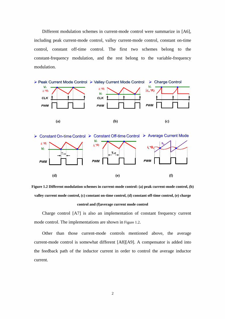
Different modulation schemes in current-mode control were summarize in [A6],
including peak current-mode control, valley current-mode control, constant on-time
control, constant off-time control. The first two schemes belong to the
constant-frequency modulation, and the rest belong to the variable-frequency
modulation.
(a) (b) (c)
(d) (e) (f)
Figure 1.2 Different modulation schemes in current-mode control: (a) peak current-mode control, (b)
valley current mode control, (c) constant on-time control, (d) constant off-time control, (e) charge
control and (f)average current mode control
Charge control [A7] is also an implementation of constant frequency current
mode control. The implementations are shown in Figure 1.2.
Other than those current-mode controls mentioned above, the average
current-mode control is somewhat different [A8][A9]. A compensator is added into
the feedback path of the inductor current in order to control the average inductor
current.

3
Figure 1.3. Average current mode controlled Buck converter
V2 control is a particular implementation of current mode control used in Buck
converters. In the inner loop, output voltage ripple is fed back to the PWM modulator.
The output capacitor equivalent-series-resistor (ESR) senses the inductor current and
feed back to the control loop. The ramp of the ripple is used as modulation ramp. The
outer loop is a compensated loop.
Figure 1.4 Architecture of V2 Control
1.2 Applications of Current-Mode Control
Due to its unique characteristics, current-mode control is indispensable to power
converter design in almost every aspect. A few applications of current-mode control
are introduced in the following paragraphs.

4
1.2.1 Voltage Regulator Application
With the development of information technology, telecom, computer and
network systems have become a large market for the power supply industry [A11].
Power supplies for the telecom, computer and network applications are required to
provide more power with less size and cost [A12][A13]. To meet these requirements,
the distributed power system (DPS) is widely adopted. As shown in Figure 1.5, the
distributed power system is characterized by distribution of the power processing
functions among many power processing units [A14]. DPS system has many
advantages, such as less distribution loss, faster current slew rate to the loads, better
standardization and ease of maintenance[A17][A18].
The paralleling module approach for point-of-load (POL) converters has been
successfully used in various power systems. The multi-phase buck converter topology
can be treated as an example to demonstrate the benefits of this approach in terms of
thermal management, reliability and power density. However, the difference between
paralleled modules will cause the current imbalanced, resulting in some units
operating with higher temperature -- a contributor to reduced reliability. Therefore,
the challenge in paralleling modular supplies is to ensure predictable, uniform current
sharing.
Figure 1.5 A typical distributed power system
There are many methods to achieve current sharing among different modules
(phases). One of the most popular methods is the active current sharing method with
5
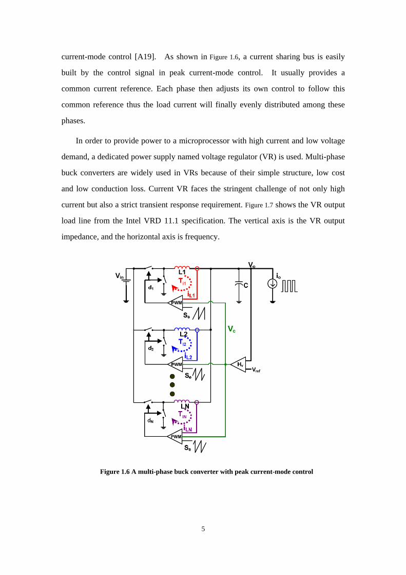
current-mode control [A19]. As shown in Figure 1.6, a current sharing bus is easily
built by the control signal in peak current-mode control. It usually provides a
common current reference. Each phase then adjusts its own control to follow this
common reference thus the load current will finally evenly distributed among these
phases.
In order to provide power to a microprocessor with high current and low voltage
demand, a dedicated power supply named voltage regulator (VR) is used. Multi-phase
buck converters are widely used in VRs because of their simple structure, low cost
and low conduction loss. Current VR faces the stringent challenge of not only high
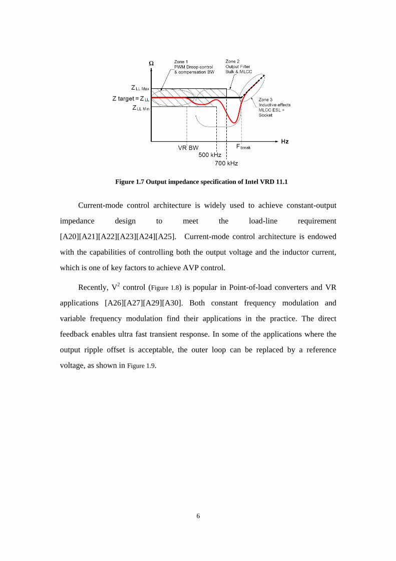
current but also a strict transient response requirement. Figure 1.7 shows the VR output
load line from the Intel VRD 11.1 specification. The vertical axis is the VR output
impedance, and the horizontal axis is frequency.
Figure 1.6 A multi-phase buck converter with peak current-mode control
6
Figure 1.7 Output impedance specification of Intel VRD 11.1
Current-mode control architecture is widely used to achieve constant-output
impedance design to meet the load-line requirement
[A20][A21][A22][A23][A24][A25]. Current-mode control architecture is endowed
with the capabilities of controlling both the output voltage and the inductor current,
which is one of key factors to achieve AVP control.
Recently, V2 control (Figure 1.8) is popular in Point-of-load converters and VR
applications [A26][A27][A29][A30]. Both constant frequency modulation and
variable frequency modulation find their applications in the practice. The direct
feedback enables ultra fast transient response. In some of the applications where the
output ripple offset is acceptable, the outer loop can be replaced by a reference
voltage, as shown in Figure 1.9.

7
Figure 1.8 Constant On-time V2 Control
Figure 1.9 Constant On-time V2 Control without outer loop
1.2.2. Power factor correction
Due to the ever-increasing requirement for improved power quality, the use of the
power factor correction (PFC) circuit for off line power supplies has been
dramatically increased. The high frequency switch mode power factor correction
converter is called a PFC stage and, it is usually inserted in the equipment to shape the
line input current into a sinusoidal waveform and its line current is in phase with the
line voltage.
8
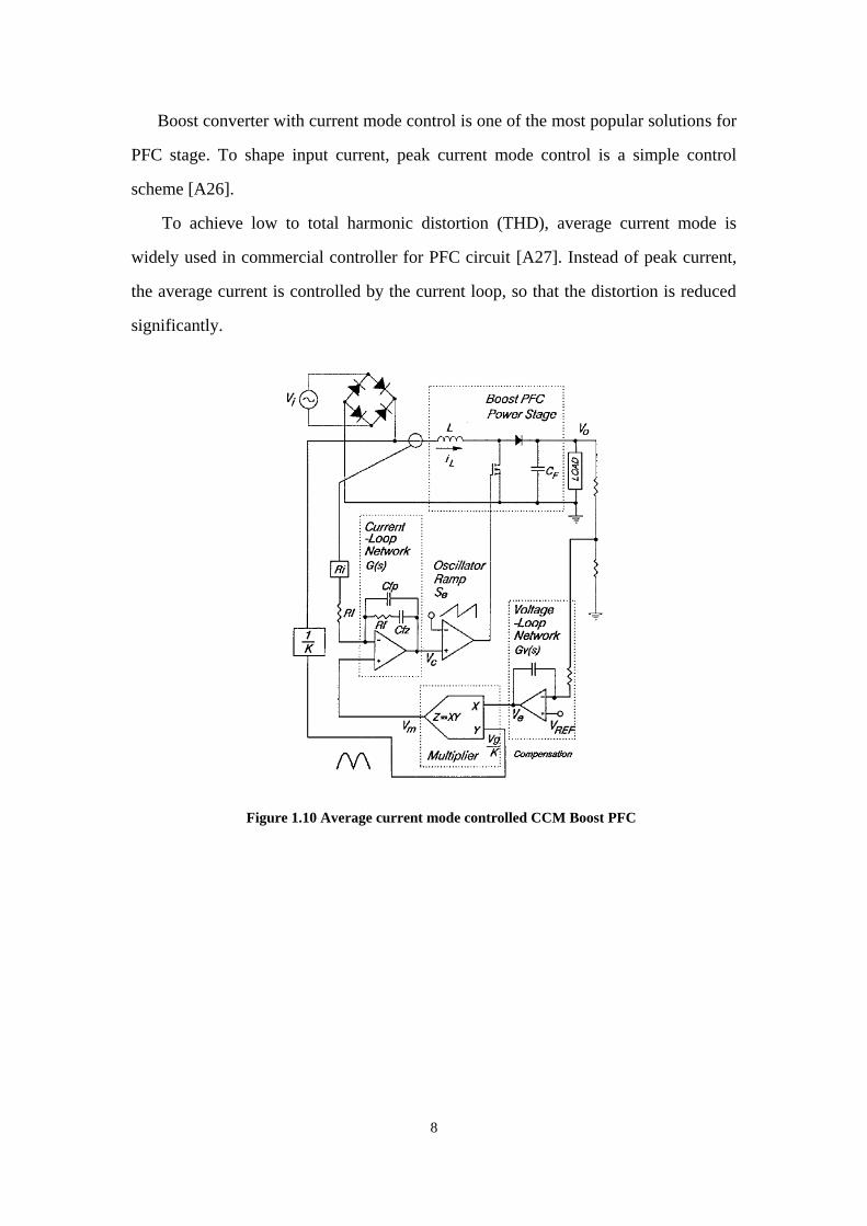
Boost converter with current mode control is one of the most popular solutions for
PFC stage. To shape input current, peak current mode control is a simple control
scheme [A26].
To achieve low to total harmonic distortion (THD), average current mode is
widely used in commercial controller for PFC circuit [A27]. Instead of peak current,
the average current is controlled by the current loop, so that the distortion is reduced
significantly.
Figure 1.10 Average current mode controlled CCM Boost PFC

9
Figure 1.11 Constant off-time current mode control CCM Boost PFC
To avoid the sub-harmonic oscillation issue, [A32] [A33]suggest a constant
off-time current mode control as the implementation of the current loop, as shown in
Figure 1.11. Constant off-time control is a variable frequency control scheme, so it also
helps to reduce the peak energy of the noise generated and simplifies the ability to
comply with EMI regulations.
For low power applications, the Flyback converter is more attractive than the
boost converter because of its simplicity. To control the average value of the pulsating
input current of the Flyback converter, charge control scheme is used in [A7]. By
employing charge control, a Flyback converter operating in CCM can achieve a unity
power factor.

10
Figure 1.12 Charge control Flyback PFC
1.2.3. Battery Charger
Batteries are commonly used in renewable generation systems, electrical
vehicles, communications systems and computer systems as electrical energy storage
elements. The major rechargeable batteries readily available today are
nickel-cadmium (NiCd), nickel-metal-hydride (NiMH), sealed-lead-acid (SLA) and
lithium-ion (Li-Ion).
Different battery chemistries have different charge requirements. NiCd and
NiMH batteries are charged with a constant-current profile. SLA and Li-Ion batteries
can be charged with a constant-voltage, current-limited supply. A typical Li-Ion
battery charge cycle begins when the voltage at battery voltage exceeds the under
voltage lockout threshold level and the IC is enabled. If the battery has been deeply
discharged and the battery voltage is less than 2.7V, the charger will begin with the
programmed trickle charge current.
When the battery exceeds 2.7V, the charger begins the constant-current portion of
the charge cycle with the charge current equal to the programmed level. As the battery

11
accepts charge, the voltage increases. When the battery voltage reaches the recharge
threshold, the programmable timer begins. Constant-current charging continues until
the battery approaches the programmed charge voltage of 4.1V or 4.2V/cell at which
time the charge current will begin to drop, signaling the beginning of the
constant-voltage portion of the charge cycle. The charger will maintain the
programmed preset float voltage across the battery until the timer terminates the
charge cycle.
Figure 1.13 Typical charge current and voltage profile
To improve efficiency, switching mode power converters are widely used in
battery charger application. To provide constant current/ constant-voltage, current
mode control power source, current mode control is the key technique in charger
controller.
The typical operation of the battery charger can be separate into two periods
[A34]. The charge current-regulation loop is in control as long as the battery voltage
is below the set point. When the battery voltage reaches its set point, the
voltage-regulation loop takes control and maintains the battery voltage at the set
point. The typical charge current and voltage profile is shown in Figure 1.13.
In smaller area and lower cost solution, charger and DC/DC converter can be
integrated in a bi-directional power converter circuit, as shown in Figure 1.14. When
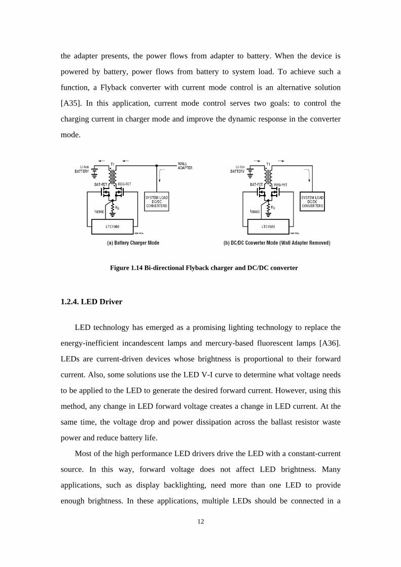
12
the adapter presents, the power flows from adapter to battery. When the device is
powered by battery, power flows from battery to system load. To achieve such a
function, a Flyback converter with current mode control is an alternative solution
[A35]. In this application, current mode control serves two goals: to control the
charging current in charger mode and improve the dynamic response in the converter
mode.
Figure 1.14 Bi-directional Flyback charger and DC/DC converter
1.2.4. LED Driver
LED technology has emerged as a promising lighting technology to replace the
energy-inefficient incandescent lamps and mercury-based fluorescent lamps [A36].
LEDs are current-driven devices whose brightness is proportional to their forward
current. Also, some solutions use the LED V-I curve to determine what voltage needs
to be applied to the LED to generate the desired forward current. However, using this
method, any change in LED forward voltage creates a change in LED current. At the
same time, the voltage drop and power dissipation across the ballast resistor waste
power and reduce battery life.
Most of the high performance LED drivers drive the LED with a constant-current
source. In this way, forward voltage does not affect LED brightness. Many
applications, such as display backlighting, need more than one LED to provide
enough brightness. In these applications, multiple LEDs should be connected in a

13
series configuration to keep an identical current flowing in each LED.
Since Buck converter output current is an inductor current, a non-pulsating
current, Buck converter without output capacitor is widely used as a LED driver due
to its simple structure, low cost and fast response. In a Buck converter without output
capacitor, controlling inductor current is controlling the LED forward current. So,
current mode control is a natural choice for Buck LED driver.
Based on the characteristics of LED, all LEDs have a relationship between their
luminous flux and forward current, IF, that is linear up to a point. Beyond that point,
increasing IF causes more heat than light. High ripple current forces the LED to spend
half of the time at a high peak current, putting it in the lower lm/W region of the flux
curve. Usually, absolute maximum ratings for peak current are close to or often equal
to the ratings for average current [A37]. High current density in the LED junction
lowers lumen maintenance, providing yet another incentive for keeping the ripple
current under control.
To achieve a constant forward current ripple, adaptive on time and constant
off-time current mode control implementation is a common solution. Adaptive on
time control changes the top switch on-time to be proportional to Vin-Vout, so that
the current ripple is kept constant with input voltage variation.
Constant off-time implementation is simpler than adaptive on-time [A38].
Forward voltage is a fix voltage under certain forward current levels, so the inductor
current down slope is determined by the output current level. By fixing the off-time of
the top switch, the inductor ripple is expressed as:
.ConstTVIofffwdripple
( 1.1 )

14
Figure 1.15 Current mode control Buck LED driver
Besides Buck, other current mode control converters are also widely used in the
LED driver design. Many of today’s portable electronics require LED-driver solutions.
Lithium-ion battery output voltage is 2.7~5.2V while typical forward voltage of each
white LED is about 3~4 volt. So, for converters designed for a single LED, such as a
digital camera flash light application, a Buck-boost converter is used [A39]. In
backlighting application, to drive a series of white LEDs with a constant current
source, a popular solution is to use a Boost or Buck-boost converter with current
mode control [A40].
1.3 Existing Models for Current Mode Controls with Proportional
Current Feedback
Current-mode control’s modulation is based on the inductor current ramp, a state
variable. Essentially, for any PWM converter with a small signal perturbation fm, the
PWM modulator generates multiple frequency components, including the
fundamental component (fm), the switching frequency component (fs) and its
harmonic (n*fs), and the sideband components (fs±fm, nfs±fm). All these frequency
components exist in the state variable of the switching circuit. In current mode control
case, inductor current is fed back to the modulator, and there is no enough attenuation
on the high frequency components. All frequency components are coupled through the
modulator, so neither the sideband components nor the switching frequency
15
components can be ignored. As a result, frequency domain analysis shows its obvious
limitation in analysis of current loop. Previous average models for current-mode
control failed to consider high frequency components.
It is relatively easy for the outer voltage loop of the current mode control
converter, since high frequency components can be attenuated due to the low pass
filter of the power stage and feedback compensation.
Due to the popularity of the current-mode control and the complexity of the
current mode control, the research on modeling current-mode control has over 30
years of history and is still on going.
Most of the early work on current mode control modeling focuses on peak
current mode control due to its popularity. In recent decades, variable frequency
current mode control, for example constant on-time control, is widely used because of
its unique advantage, such as high light load efficiency and simple implementation.
The modeling of variable frequency current mode control has gained more attention
recently.
To review the previous modeling work for current mode control, the modeling
methodologies can be categorized into several groups and listed as follows.
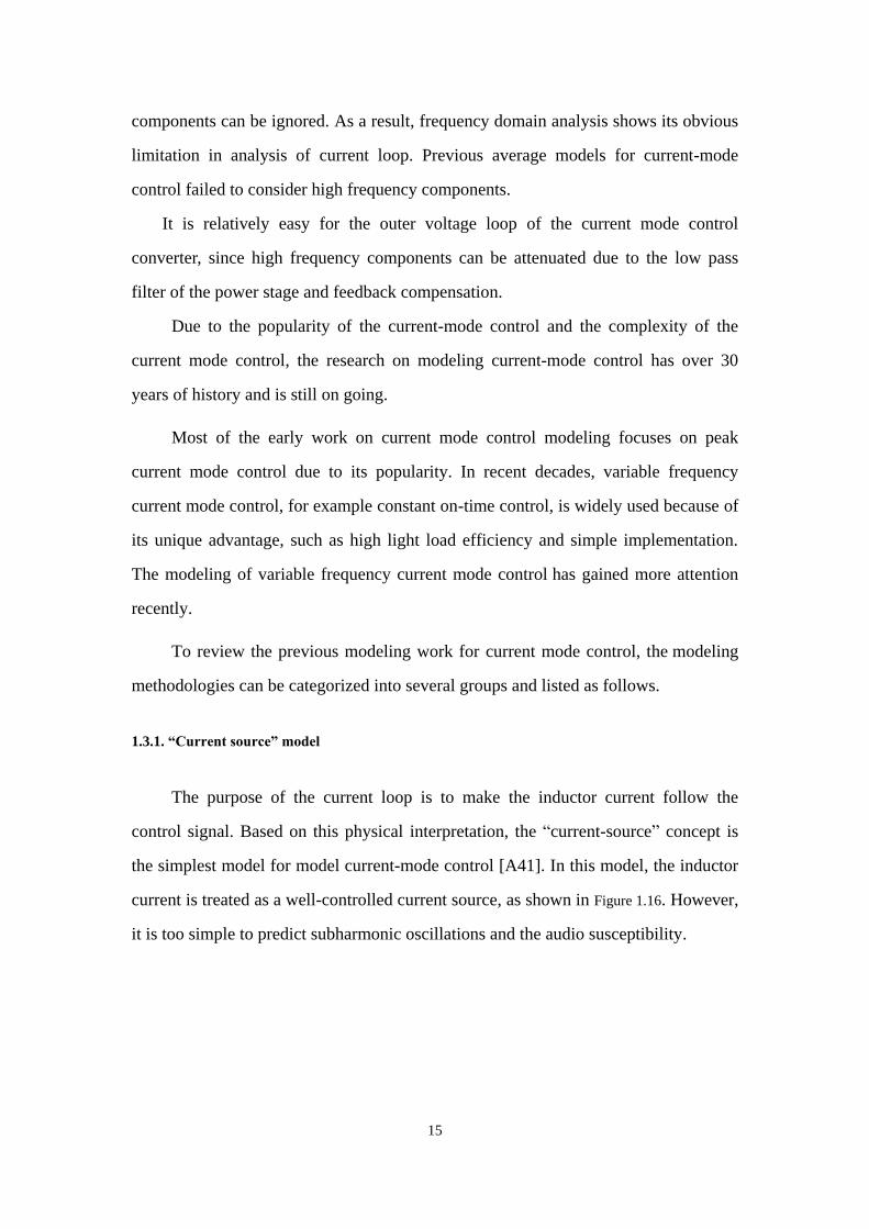
1.3.1. “Current source” model
The purpose of the current loop is to make the inductor current follow the
control signal. Based on this physical interpretation, the “current-source” concept is
the simplest model for model current-mode control [A41]. In this model, the inductor
current is treated as a well-controlled current source, as shown in Figure 1.16. However,
it is too simple to predict subharmonic oscillations and the audio susceptibility.

16
(a)
(b)
Figure 1.16 current-mode control: (a) control structure, (b) “current source” concept
1.3.2 Average model
Under purturbation, although a switching converter generates many side band
components, since there must be a low-pass filter in the power stage, the average
concept, which only capture the modulation frequency information, can be sucessfully
used in the modeling of the switching converter [A42] [A43] [A44] [A60] [A45][A46]
[A47] [A48]. Based on average models for power stage, the average models for peak
current-mode control are developed[A49] [A50][A51][A52][A53] [A54][A55][A56]
[A57] [A58][A59].
In the current loop, averaged inductor-current information is fed back to the
modulator with pure sensing gain. Modulator gain Fm, is derived by geometrical
calculations, assuming a constant inductor current ramp and an external ramp. In
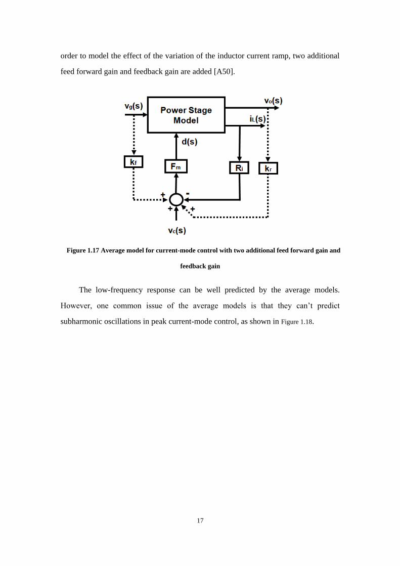
17
order to model the effect of the variation of the inductor current ramp, two additional
feed forward gain and feedback gain are added [A50].
Figure 1.17 Average model for current-mode control with two additional feed forward gain and
feedback gain
The low-frequency response can be well predicted by the average models.
However, one common issue of the average models is that they can’t predict
subharmonic oscillations in peak current-mode control, as shown in Figure 1.18.

18
Figure 1.18 Control-to-output transfer function comparison (D=0.45)
1.3.3 Discrete-time model and sample data model
(a) (b)
Figure 1.19 Discrete-time analysis: (a) natural response, and (b) forced response
In peak current-mode control, the inductor current error stays the same for one
switching cycle, until the next sampling event occurs. This behavior is similar to a
discrete time system. Based on this concept, the discrete-time model for current mode

19
control is proposed by D. J. Packard [A60] and A. R. Brown [A61]. The analytical
prediction of the current loop instability in peak current-mode control was first
achieved.
Based on the time-domain waveform of the inductor current, as shown in Figure
1.19, the response of the inductor current is divided into two parts, including the natural
response and the forced response. The discret-time expression can be found as:
Natural response: )(ˆ)1(ˆ kikiLL
( 1.2 )
Forced response: )1(ˆ/)1()1(ˆ kvRkiciL
( 1.3 )
where )/()(enef
ssss , sn is the magnitude of the inductor current slope during
the on-time period, sf is the magnitude of the inductor current slope during the
off-time period, se is the magnitude of the external ramp, and Ri is the sensing gain of
the inductor current.
Based on the combination of two parts, the control-to-inductor current transfer
function in the discrete-time domain can be calculated as:
z
z
Rzv
zizH
ic
L1
)(
)(ˆ)(
( 1.4 )
The discrete-time transfer function shows that there is a pole located at α. The
system stability is determined by the absolute value of α, which is a function of sn, sf,
and se. The absolute value of α has to be less than 1 to guarantee system stability.
For example, when se=0 and sn<sf (D>0.5), the absolute value of α is larger than 1,
which means the system is unstable. This model can accurately predict subharmonic
oscillations and the influence of the external ramp in peak current-mode control and
valley current-mode control.
In order to model peak-current mode control in the continuous-time domain
instead of the discrete-time domain, sample-data analysis by A. R. Brown [A61] is
performed to explain the current-loop instability in the s-domain.

20
Although the discrete-time model and sampled-data model can precisely predict
the high-freqeuncy response, it is hard to use, just like the discrete-time model.
1.3.4 Modified average model
In order to extend the validation of the averaged models to the high-frequency
range, several modified average models are proposed based on the results of
discrete-time analysis and sample-data analysis [A62][A63] [A64] [A65][A66] [A67]
[A68][A69][A70].
One of popular models is investigated by R. Ridley [A64], which provided both
the accuracy of the sample-data model and the simplicity of the three-terminal switch
model. Essentially, R. Ridley’s modeling strategy is based on the hypothesis method.
In this method, first, the control-to-inductor current transfer function is obtained by
transferring previous accurate disctrete-time transfer function ( 1.5 ). into its
continuous-time form:
sw
sw
sT
sT
swic
L
e
e
sTRsv
si 111
)(
)(
( 1.5 )
Then, “sample and hold” effects are equivalently represented by the He(s)
function which is inserted into the feedback path of the inductor current in the
continuous avarge model, as shown in Figure 1.20. Another form of the
control-to-inductor current transfer function can be calculated based on this assumed
average model:
)()(1
)(
)(
)(
sHRsFF
sFF
sv
si
eiim
im
c
L
( 1.6 )
Finally, based on ( 1.6 ) and ( 1.7 ), the He(s) function is obtained as
1)(
swsT
sw
e
e
sTsH
( 1.7 )
Following the same concept used in [A50], the complete model is completed by
adding two additional feed-forward gain and feedback gain. Due to its origination

21
from the discrtete-time model, there is no doubt that this model can accurately predict
subharmonic oscillations in peak current-mode control and valley current-mode
control. According to the control-to-output transfer function, as shown in Figure 1.21,
the position of the double poles at high frequency is determined by the duty cycle value.
Figure 1.20. R. Ridley’ model for peak current-mode control
Figure 1.21 Control-to-output transfer function based on R. Ridley’ model (se = 0)
Another modified models is proposed by F. D. Tan and R. D. Middlebrook [A66].
In order to consider the sampling effects in the current loop, one additional pole needs
to be added to a current-loop gain derived from the low-frequency model, as shown in
Figure 1.22.

22
Figure 1.22. F. D. Tan and R. D. Middlebrook’s model for peak current-mode control
Further analysis based on the modified models above is discussed for peak
current-mode control [A68][A69][A70]. The models for average current-mode
control and charge control are obtained by extending the modified average model
[A71][A72][A73].
So far, R. Ridley’s model is the most popular model for system design.
1.3.5 Continuous time model
In constant frequency peak current-mode control, the inductor current error
varies at switch off instant and stays the same for one switching period. This is called
the “sample and hold” effect.
For variable frequency modulation current mode control, the current-loop
behavior is different from that in peak current-mode control. For example, in constant
on-time control, as shown in Figure 1.23, the inductor current goes into steady state in
one switching period. No “sample and hold” effects exist in constant on-time conrol.

23
(a)
(b)
Figure 1.23. Perturbed inductor current waveform: (a) in peak current-mode control, and (b) in
constant on-time control
Figure 1.24. Discrepancy in the extended model
Discrete-time analsys and sample-data analysis is only applicable to a constant
frequency sampling system. They can’t be applied to variable frequency current mode
control. Figure 1.24 shows that R. Ridley’s extended model to constant on-time control
[A74] is not very good at predicting the small signal behavior of the switching circuit.
To solve this issue, a continuous time model is proposed in [A75]. The inductor,
the switches and the PWM modulator are treated as a single entity to model instead of

24
breaking them into parts to do it. As shown in Figure 1.25, a sinusoidal perturbation with
a small magnitude at frequency fm is injected through the control signal vc; then, based
on the perturbed inductor current waveform, the describing function [A76] from the
control signal vc to the inductor current iL can be found by mathematical derivation.
The same method is applied two derive two additional terms that represent the
influence from the input voltage vin and the output voltage vo.
Figure 1.25. Perturbed inductor current waveform in peak current-mode control
This approach can be applied not only to constant-frequency modulation but also
to variable-frequency modulation. The accuracy of the model is not limited by the
frequency range. The fundamental difference between different current-mode controls
is elaborated based on the models obtained from the new modeling approach.
Essentially, the current mode control converter is an infinite order system. For
practical design purposes, the system can be simplified as a third order system. In
control to output transfer function, a single pole determined by load is at low frequcny
and a pair of high frequency double poles are located at high freqency. The position of
the double pole located at the high frequency is different for constant frequency
modulation and variable frequency cases. For constant frequency modulation, the
location of the double poles locate is at 1/2 fsw and it is possible for them to move to
the right half plane. For variable frequency modulation, the double poles location is
determined by Ton or Toff, and the double poles never move to the right half plane.
That means the variable frequency modulation current loop is always stable.

25
Although the continous time model using the describing fucntion method
provides an accurate enough model, the mathmatical derivation is too complicated for
practical use.
For a current mode control Buck converter, to simply represent the output
voltage transfer function co
vv ˆ/ˆ and input to output transfer function ino
vv ˆ/ˆ and
output impedance, an equivalent circuit was proposed, as shown in Figure 1.26. The
resonant of the equivalent capacitor Ce and Ls characterize the high frequcny double
pole and Re represents the damping effect.
Figure 1.26. Equivalent circuit for current mode control Buck converter
However, this equivalent circuit is not a complete model for a current mode
control Buck converter since the input current property is lost. Moreover, no
equivalent circuit of other current mode control converters are available.
1.4 Existing Models for Other Current Mode Controls
1.4.1 Average Current Mode Control
The early models of average current mode control are based on state variable
averaging concept [B4][B5][B6][B7][B8]. The models consider only the perturbation
frequency component in the current feedback loop. The PWM comparator is modeled
as the pure gain transfer function 1/Vramp, where Vramp is the peak-to-peak voltage of
the artificial ramp signal. These models do not predict the sub-harmonic instability.

26
Instead, [B4] suggests that applying external ramp excess the ripple slope at current
compensator output would guarantee the current loop stability.
Figure 1.27. Average model for Average current mode control
Another popular model was proposed by Tang [B13]. The block diagram of this
model is shown in Figure 1.28. This model tries to consider nonlinearity of the current
loop to predict the sub-harmonic instability in frequency domain model. This model
assumed that the same sample-and-hold effect in peak current model control also
exists in average current mode control, so the He(s) term is inserted in the current
feedback path without solid justification. The modulator gain Fm was derived in [B13]
considering the switching ripple of vcom. This model models the average current mode
control as a third order system, which has a pair of double pole at half of switching
frequency. When the quality factor of this double pole becomes negative, the current
loop is unstable. The criteria of designing the compensator to shape the current loop
gain and avoid instability were proposed in this paper.
However, in fact, the accuracy of this model is not satisfactory. It is unreasonable
to assume the current compensator has different transfer function in voltage loop and
current loop. Also, the He term in average current mode is not justified. Due to these
debatable assumptions, the accuracy of this model is questionable.

27
Small signal model based on the Krylov–Bogoliubov–Mitropolsky (KBM)
algorithm [B16] and describing function [B17] provides pretty accurate prediction,
but the mathematical derivation is very complicate and lacking physical insight.
Figure 1.28. Modified average model for average current model control
1.4.2 V2 control
As shown in Figure 1.29, [C7] models constant frequency V2 control using the
modified average model for peak current mode control. It tries to consider the effect
of the ripple of capacitor but still borrowed the sample & hold concept of peak current
mode control without justification As a result, the conclusion that capacitor ripple
increase double damping is incorrect. More important, sample & hold concept is not
applicable in variable frequency modulations [C8], so the most popular constant
on-time V2 control cannot be analyzed based on this concept.

28
Small signal model based on describing function provides a good model for
control-to-output transfer function and output impedance in practical design range
[C9]. It treats the power stage and inner feedback loop as an entity. All the sideband
frequency feedback effect is considered in this entity. An accurate criteria of stability
is provided by this model. However, the mathematical derivation of this model is very
complicated and time consuming. Moreover, it assumes that the inductor current
slopes are constant value. Theoretically, the assumption is not justified. It results in
the accuracy of the model in the case with large external ramp is questionable.
Figure 1.29 Model for V2 Control based on modified average model of current mode control
Figure 1.30 Modeling of V2 control based on describing function

29
Literature [C10] proposed an equivalent circuit model for V2 control, as shown in
Figure 1.31, but a significant problem is its equivalent circuit failed to explain the
output impedance characteristic of V2 control. Furthermore, many transfer functions,
such as input impedance, are not included in this incomplete model.
Figure 1.31 Equivalent circuit model in [C10] of V2 control
1.5 Dissertation Outline
This dissertation consists of seven chapters. They are organized as follows. First,
the application background and the history of small signal modeling of current mode
control are introduced. Then, the proposed three-terminal switch equivalent circuit
model is presented. Using this unified model, average current mode control is
analyzed and new design guidelines are proposed. Next, the application of the
proposed equivalent circuit model is extended to the analysis of V2 control. After that,
a novel average current mode control architecture is proposed. At last, the equivalent
circuit is applied to the Laplace domain model of digital predictive current mode
controls.
The detailed outline is elaborated as follows.
Chapter 1 is the review of the application of current-mode control and the
modeling techniques. Current-mode control architectures with different
implementation approaches have been widely used in many applications, such as

30
voltage regulator, power factor correction, battery charger and LED driver. An
accurate model for current-mode control is indispensable to system design. However,
available models can only solve partial issues. The continuous time model based on
describing function is one of the accurate approaches to model current mode controls,
but the mathematical derivation is too complicated that the application in engineering
design is limited. The primary objective of this dissertation is to develop a unified
three-terminal switch model for current-mode control with different implementation
methods which are applicable in all the current mode control power converters.
In Chapter 2, a unified three-terminal switch model for current mode control is
presented. Based on the observation, the PWM switch and the closed current loop is
taken as an invariant sub-circuit which is common to different PWM converter
topologies. The Basic small signal relationship is studied and the result shows that the
PWM switch with current feedback preserves the property of the PWM switch in
power stage. A three-terminal equivalent circuit is developed to represent the small
signal behavior of this common sub-circuit. The proposed model is a unified model,
which is applicable in both constant frequency modulation and variable frequency
modulation. Proposed model is extended to multiphase configurations. Based on the
unified model, the merits and limits of different implementations are compared.
After that, the Laplace domain small signal model for digital predictive current
mode control is proposed. The describing function method is applied to derive the
small signal model. The model covers peak current mode, valley current mode and
average current mode control with various modulations. The model is also extended
to multi-sampling cases. Design guidelines and comparison of modulation laws are
discussed. The modeling results are summarized as equivalent circuit model.
In Chapter 3, the small signal equivalent circuit model is extended to average
current mode control. It is shown that many existing models do not consider the ripple
of current compensator in a correct way. As a result, the accuracy of model at high
frequencies is unsatisfactory. By separating the feedback information of average
current mode control, the equivalent circuit model for average current mode control
31
using the proposed equivalent circuit is presented. The model includes the sideband
frequency feedback effect so that it is accurate up to half of switching frequency. The
design guidelines are investigated.
In Chapter 4, the small signal equivalent circuit model is extended to V2 current
mode control and enhanced V2 control. V
2 control is decomposed as current mode
control with proportional capacitor voltage feedback and load current feedback. The
load current feedback effectively reduces the output impedance. For Voltage
Regulator applications, the enhanced V2 control is a variety of V
2 control with
additional inductor current feedback to the output voltage. The enhanced V2 control is
analyzed using the equivalent circuit model in this chapter.
In Chapter 5, I2 average current mode control is proposed. I
2 current mode
control has two inductor current feedbacks: one is the direct feedback without low
pass filter, and the other one is the integral feedback. The small signal analysis based
on the proposed equivalent circuit model is presented. The concept of I2 control is
applicable to both constant frequency and variable frequency modulations. As a
particular embodiment, constant on-time I2 control is proposed to improve both
transient response and light load efficiency of average current mode control.
Chapter 6 is the summary of the dissertation.

32
Chapter 2. Unified Three-Terminal Switch Model for
Current Mode Controls
This chapter introduces a new unified three-terminal switch mode for
current-mode controls. The proposed model takes the active switch, passive switch
and the closed current loop as an invariant entity, which is a common sub-circuit for
different topologies, and uses the three-terminal equivalent circuit to represent the
small signal behavior of this common sub-circuit in current mode control power
converter. The derivation process utilizes the small signal relationship between the
terminal voltage and the current, which are obtained from describing function method.
The proposed model is a unified model, which is applicable to constant frequency
peak current mode control, valley current mode control and charge control, and
variable frequency constant on-time control and constant off-time control. Small
signal model for commonly used topologies with current mode control can be easily
obtained by replacing the three-terminal switch with the current feedback loop, by the
three-terminal small signal equivalent circuit point by point.
2.1 Common Invariant Structure in Current Mode Control
Power Converters
Current-mode control has unique advantages over voltage mode control, such as
fast dynamic response and inherent current limit. It is also an indispensable technique
to achieve current sharing and, AVP control. As a result, current mode control has
been widely used in the power converter design. The most commonly used power
converter topologies are Buck, Boost, Buck-boost, Flyback, forward and some other
topologies derived from these basic ones.

33
Figure 2.1. Current mode control DC/DC converters
Basic current mode control power converters are shown in Figure 2.1. Although
topologies are different, they have basic structure in common. It consists of an active
switch, a passive switch, inductor and a closed current loop. The common node active
switch and passive switch connects to the inductor. The terminal designations a,p,c
refer to active, passive, and common respectively. vc is the control signal, which is the
output of the voltage loop compensator. The common three-terminal structure is
shown in Figure 2.2.

34
This three-terminal structure is an extension of the three-terminal switch of power
stage. It is the only non-linear device of the power converter. Take the three-terminal
structure as a basic building block of current mode control converters, then converters
can be obtained by a simple cyclic permutation of the three-terminal switch and
connecting external linear components to it. All the ports of the three-terminal switch
should be connected to voltage ports as indicated in Figure 2.2. By modeling this
common building block with an equivalent circuit, small signal equivalent circuits for
current mode control power converters can be obtained by substituting the
three-terminal switch with its equivalent circuit point-to-point.
Figure 2.2. Common invariant structure in current mode control power converters
2.2 General Small Signal Relationship for Three-terminal
Switch
A three-terminal switch with current feedback loop is an extension of
three-terminal switch of power stage. The closed current loop is added to the power
stage three-terminal common structure and the inductor is included into the common
block.
In [A47], a small signal relationship is derived based on instantaneous voltage
and current waveform. Current in the active terminal is always the same as the current
in the common terminal during the switch ON-interval DTsw, and equals to zero
during the switch OFF-interval. The expression of active switch current is given by

35
( 2.1 ). The waveform is shown in Figure 2.3. This description is true no matter which
configuration the switch is implemented in.
swsw
swc
aTtDT
DTttiti
,0
0),()(
( 2.1 )
Figure 2.3. Basic waveform of PWM switch
Using average concept, average terminal currents ia, and ic, we have from very
simple relations:
caidi
( 2.2 )
Perturb the ( 2.2 ) and neglect the high order term, a small signal relationship
between ia and ic is derived as ( 2.3 ).
ccaIdiDi ˆˆˆ
( 2.3 )
Essentially, the (2.3) is an average model and it can be proved that is it accurate
up to 1/2 fsw. The instantaneous current relationship is given by ( 2.1 ) is valid as long
as the PWM power converter works in continuous current mode, regardless of the
implementation of the pulse-width modulator.
For the three-terminal switch under current mode control, since all the
assumption used in deriving ( 2.1 ) is not violated, the small signal given by ( 2.3 ) is
also true. This conclusion is verified by the Simplis simulation. Using peak current

36
mode control as an example, d to ia transfer function obtained from simulation and
average model are compared in Figure 2.4. From ( 2.3 ), an average model is written as:
c
caI
d
iD
d
i
ˆ
ˆ
ˆ
ˆ
( 2.4 )
Figure 2.4. Duty cycle to switch current transfer function (fixed frequency modulation)
A similar comparison for constant on-time current mode control is shown in Figure
2.5.
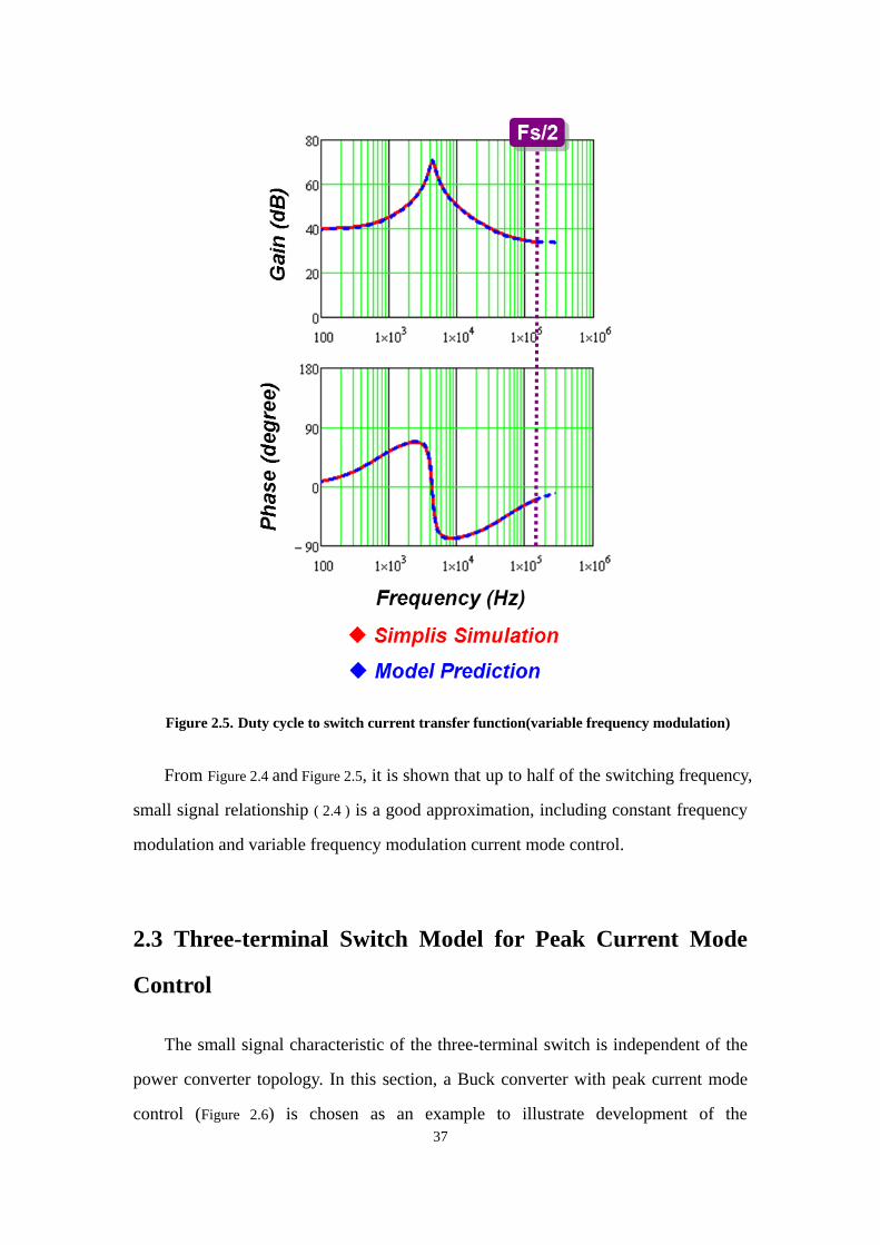
37
Figure 2.5. Duty cycle to switch current transfer function(variable frequency modulation)
From Figure 2.4 and Figure 2.5, it is shown that up to half of the switching frequency,
small signal relationship ( 2.4 ) is a good approximation, including constant frequency
modulation and variable frequency modulation current mode control.
2.3 Three-terminal Switch Model for Peak Current Mode
Control
The small signal characteristic of the three-terminal switch is independent of the
power converter topology. In this section, a Buck converter with peak current mode
control (Figure 2.6) is chosen as an example to illustrate development of the

38
three-terminal switch model.
2.3.1 Review of Equivalent Circuit for Current Mode Control Buck Converter
without Input Current Property
Figure 2.6. Current mode control Buck converter
Literature [A75] proposes a modeling strategy that models a current mode control
DC/DC converter based on continuous time model. It takes the Buck converter power
stage and the closed current loop as an single entity, and uses describing function
method to derive control to the output voltage transfer function co
vv ˆ/ˆ and input to
output transfer function ino
vv ˆ/ˆ . This method is applicable not only to a constant
frequency modulation current mode control, but also to a variable frequency
modulation current mode control. The exact model derived by this method is accurate
beyond the switching frequency.
For simplicity, literature [A75] proposes an equivalent circuit to represents the
control to output voltage transfer function co
vv ˆ/ˆ and input to output transfer function
inovv ˆ/ˆ
for a current mode control Buck converter. The equivalent circuit model is
good up to half of the switching frequency.
The equivalent circuit is shown in Figure 2.7.

39
Figure 2.7. Equivalent circuit for current mode control Buck converter
In Figure 2.7, the parameters are defined as Table 2.1:
Table 2.1. Parameters Definition of Equivalent Circuit (Figure 2.7)
Peak current mode control
)]5.0(/[
fn
en
swsess
ssTLR
2
2
s
sw
eL
TC ][
2
1
22
off
s
in
T
QL
DK
Valley current mode control
)]5.0(/[
fn
ef
swsess
ssTLR
2
2
s
sw
eL
TC ][
2
1
22
on
s
in
T
QL
DK
Charge control
)](/[
sw
T
f
e
swcp
Ls
swseT
C
s
sD
TV
ILTLR
2
2
2
s
sw
eL
TC ][
2
1
2
on
cs
in
T
QL
DK
Constant on-time control
onseTLR /2
)/(
22
soneLTC
)/(
soninLTK 2
Constant off-time control
offseTLR /2
)/(
22
soffeLTC
0
inK
This equivalent circuit correctly represents the inductor current property under
control signal perturbation and input voltage and output voltage perturbation, but
switch current and diode current properties are lost.
To correctly represent the small signal behavior of the three-terminal structure

40
(Figure 2.2), the equivalent circuit should have three terminals corresponding to the
switch model. In such a three-terminal structure, if two terminal currents are correctly
represented, the accuracy of the third terminal current is guaranteed by Kirchhoff's
Current Law. Since the equivalent circuit in Figure 2.7 represents the inductor property,
it is a good starting point when building the three-terminal equivalent circuit.
2.3.2 Complete Equivalent Circuit for Current Mode Control Buck Converter
The equivalent circuit Figure 2.7 accurately represents the property of the common
terminal current. The strategy of deriving a three-terminal equivalent circuit is
modifying the equivalent circuit in Figure 2.7, keeping the inductor current and adding
a proper part to represent the active switch current. The correctness of the passive
switch current property is guaranteed by Kirchhoff's Current Law.
The equivalent circuit is redrawn in Figure 2.8 with the introduction of a DC
transformer with turns ratio D, which is the steady state duty cycle. On the secondary
side, the inductor terminal is defined as c corresponding to the circuit diagram. On the
primary side, the terminal a and p are defined by the corresponding circuit diagram.
The in
v̂ controlled current sourceinin
kv ˆ in Figure 2.7 is equivalently represented by
input voltage in
v̂ together with an input voltage controlled voltage source apin
Kv ˆ ,
where ap
K is defined as:
1
D
RKK
ein
ap ( 2.5 )
Since Ce forms double poles with Ls at half the switching frequency, at low frequency
range, the DC transformer secondary side current ire is approximately equal to iL. As
a result, the primary side current is given by:
cpriiDi ˆˆ
( 2.6 )

41
Figure 2.8. Equivalent circuit with DC transformer
Compare this equivalent circuit with the universal relationship between ia and ic,
the term ciD ˆ is represented by the DC transformer, but the missing term c
Id ˆ is
not shown in the circuit. To correctly represent this relationship, a current source
should be added between terminal a and p.
Under the small signal perturbation of control voltage c
v̂ and the small signal
perturbation of input voltage in
v̂ , as a response, the output voltage has a small signal
perturbation o
v̂ . Using the modeling strategy used in [A75], the three-terminal
switch is taken as an entity. The describing function method is used to model control
to the duty cycle transfer function. The duty cycle small signal modulation can be
expressed by:
2
2
2
22
2
2
2
22
2
2
2
2
2
2
22
1
11
1
211
1
//)(
//
]/)/([)(
//)(ˆ
sQsVsv
sQs
ssTD
Vsv
sQs
s
VR
Lsvd
cp
cp
off
ap
ap
api
s
c
where
).(
,/
50
122
fn
en
sw
ss
ssQT
( 2.7 )
Based on ( 2.7 ), the cId ˆ term is expressed by:

42
2
2
2
22
2
2
2
22
2
2
2
2
2
2
22
1
1
1
21
1
//)(
//
]/)/([)(
//)(ˆ
sQsV
Isv
sQs
ssTD
V
Isv
sQs
s
VR
ILsvId
ap
c
cp
off
ap
c
ap
api
cs
cc
( 2.8 )
In the small signal equivalent circuit Figure 2.8, under small signal perturbation of
control voltage c
v̂ , and the small signal perturbation of input voltage ap
v̂ , the output
voltage small signal perturbation is cp
v̂ . Then, the inductor voltage small signal
response L
v̂ can be easily obtained:
]//
[)(
]//
])/(/[)[(
//)(ˆ
11
1
1
21
1
2
2
2
22
2
2
2
22
22
2
2
2
22
sQssv
sQs
sDTQsv
sQs
s
R
Lsvv
cp
off
ap
i
s
cL
(2.9)
When compare ( 2.8 ) and (2.9), it is found that they have similar dynamic terms.
So, the equation for cId ˆ can be rearranged and expressed by
Lv̂ in a simple way:
apapcpcpLL
c
ap
ap
ap
c
cpcp
off
ap
i
s
c
ap
c
c
RvGvGv
ID
Vsv
V
Isv
sQssv
sQs
sDTQsv
sQs
s
R
Lsv
V
IId
/ˆˆˆ
)/()()(]}//
[)(
//
])/(/[)(
//)({ˆ
11
1
1
21
1
2
2
2
22
2
2
2
22
22
2
2
2
22
where c
ap
ap
ap
c
cpLDI
VR
V
IGG ,
(2.10)
According to (2.10), the equivalent circuit Figure 2.8 is modified to represent the
switch current. Three branches corresponding to the terms in (2.10) are added between
terminal a and terminal p. The complete equivalent circuit for the peak current mode
control Buck converter is Figure 2.9.

43
Figure 2.9. Complete equivalent circuit for peak current mode control Buck converter
2.3.3 Three-terminal Switch Mode for Peak Current Mode Control
Comparing the circuit diagram with the small signal equivalent circuit, the linear
part in the circuit is kept the same as in the equivalent circuit, and the common
three-terminal structure is replaced by a three-terminal equivalent circuit. Since the
previous derivation is independent of topology, this three-terminal equivalent circuit
is the small signal equivalent circuit for the common structure. The three terminal
equivalent circuit model for the peak current mode control is shown in Figure 2.10.
Figure 2.10. Three terminal equivalent circuit model for peak current mode
control
2.4 Discussion on Physical Meaning of Three-Terminal
Switch Model
Clear physical meaning can be found based on the equivalent circuit model. In
practical design range (with small external ramp), Re is a relatively large resistor. The

44
power stage double poles formed by Ls and Co are split. One pole moves to a lower
frequency. That’s the reason why the system behaves like a first order system in
low-frequency range. The other pole moves to high-frequency and combines with a
high-frequency pole, resulting in a double pole at half of the switching frequency. For
a duty cycle larger than 0.5 case, Re becomes negative which makes the double move
to the right half of the plane and predicts sub-harmonic oscillations.
If a large external ramp is added to the current loop, the current control effect is
weakened. For the external ramp se>>sn,sf, Re is reduced to a negligible value (2.11).
High frequency double poles split and the power stage filter double poles recover.
Since Re is very small, the pole related to Re and Ce is much higher than 1/2 the
switching frequency. As a low frequency model, Ce is negligible in this case.
0
e
fn
sw
s
es
ss
T
LR
(2.11)
With se>>sn,sf, parametersap
K , i
e
cRD
Rv
ˆ and the primary current branch
LLcpcp
ap
apGvGv
R
v ˆˆ
ˆ can be simplified as (2.12) ~(2.14).
02
e
fn
sw
aps
ss
T
DK
(2.12)
D
Vd
D
V
sTv
RD
Rv
inin
esw
c
i
e
c
ˆ)ˆ(ˆ
1
(2.13)
cLLcpcp
ap
apIdGvGv
R
v ˆˆˆ
ˆ
(2.14)
Based on (2.12) ~(2.14), an important property is revealed: the equivalent circuit is
a unified model showing the unification of the current mode control and voltage
control. With the external ramp increase, the current control effect is weakened. If
se>>sn,sf, current feedback information is negligible, the three-terminal switch mode
for current mode control degenerates to a three-terminal switch mode for the power
stage [A47], as shown in Figure 2.11.

45
Figure 2.11. Three terminal equivalent circuit model degenerates to
three-terminal switch mode for the power stage when se>>sn,sf
2.5 Model Extension to Other Current Mode Controls
The proposed modeling strategy can be used for other types of current-mode
control structures, including valley current-mode control, charge control and constant
on-time control and constant off-time control structures. For constant frequency
modulation, an external ramp with slope se is added to help stabilize the current loop.
For constant on-time control and constant off-time control, since no external ramp is
needed to stabilize the current loop, the external ramp is not considered in the model.
The circuit parameters are shown in Table 2.2.
For constant frequency modulation current mode controls, the resonant frequency
of Ls and Ce is located at half of the switching frequency, and the resistance of Re
could be positive or negative, depending on the duty cycle and load current. Negative
Re indicates that the current loop is unstable, suffer to sub-harmonic oscillation. Using
an external ramp can help to stabilize the current loop and achieve a proper damping
of the double poles at half of the switching frequency.
For variable frequency modulation current mode control, the resonant frequency

46
of Ls and Ce is located at a certain frequency higher than half of the switching
frequency, which is determined by Ton or Toff, and the resistance of Re is always
positive. This circuit can be used to illustrate the instability of the current loop. The
key transfer functions, including the control-to-output transfer function, the audio
susceptibility, and the input impedance and output impedance, can be easily
calculated based on the equivalent model.
Figure 2.12. Unified three terminal equivalent circuit model for current mode controls
Table 2.2. Parameters Definition of Three-terminal Switch Model (Figure 2.12)
Peak current mode control
)]5.0(/[
fn
en
swsess
ssTLR
2
2
s
sw
eL
TC
e
s
off
apR
L
TK
2
Valley current mode control
)]5.0(/[
fn
ef
swsess
ssTLR
2
2
s
sw
eL
TC
e
s
off
apR
L
TK
2
Charge control
)](/[
sw
T
f
e
swcp
Ls
swseT
C
s
sD
TV
ILTLR
2
2
2
s
sw
eL
TC e
s
on
apR
L
TK
2
Constant on-time control
onseTLR /2
)/(
22
soneLTC
onoffapTTK /
Constant off-time control
offseTLR /2
)/(
22
soffeLTC
1
apK

47
2.6 Three-Terminal Switch Model for Digital Predictive
Current Mode Controls
Analog current mode control has been widely used in power converter design for
several decades due to the simplification of compensation and improvement of
dynamic performance [E1].
Small signal model of analog current mode control has been studied for more
than three decades. Generally, in PWM converters, under single frequency
perturbation, PWM modulator generates sideband frequency components so that the
state variables contain not only fundamental frequency but also sideband frequency
components. In current mode controlled PWM converter, since there is no low pass
filter in current feedback path, sideband frequency components couple with the
fundamental component through the output of a PWM modulation. As a result, current
loop is a highly nonlinear circuit [E2].
State space average model does not consider the effect of sideband frequency
component feedback, so it cannot predict sub-harmonic oscillation phenomenon [E3].
R.Ridley’s model [E4] is successful in peak/valley current mode control, well
predicting the sub-harmonic instability. Essentially this model is based on the fact that
in peak/valley current mode control, inductor current error updates once per switching
cycle and holds until next cycle. However, this description is only true in single edge
modulation. Recently, in [E2], the closed current loop is treated as an entity and
describing function method is used to derive accurate Laplace-domain model. The
current-loop sideband effects can be identified through the time-domain waveform,
which includes all the effects of the dynamic nonlinearity of the modulator. This
method is applicable to any modulation law since it is based on the description of
continuous time domain inductor current waveform.
Digital control techniques receive particular attention recently for
programmability, integration enhancements, auto-tuning and communication features
48
[E5][E6]. Taking the advantage of current control and digital control, digital current
mode control is applied in a number of applications, such as UPS system [E7] and
electric vehicles [E8]. To solve the issue of high frequency wide dynamic range
current sampling, predictive current mode control is one of the promising
implementation for its fast dynamic response [E14]. Many implementations were
proposed in past ten years. Peak current control, valley current control and average
current control with single edge, symmetrical double edge and asymmetrical double
edge modulation were presented in [E9]-[E15].
In order to understand the advantage and the limitations of each implementation
and choose the modulation scheme and design the control loop, precise small signal
model is indispensable. In [E9]-[E13], the boundary condition of instability were
predicted by geometrical relations of inductor current error ΔiL between two adjacent
switching cycle, but essentially these analyses were not frequency domain small
signal modeling. The complete small signal models were not provided to evaluate the
stable margin and design the compensator. As mentioned before, in the small signal
modeling for analog current mode control, state space average modeling technique
[E3] cannot predict sub-harmonic instability. Conventional Z-domain model is based
on the discretization of the state space average model [E20][E21], so that the accuracy
at high frequency is also questionable in current mode control, especially for
multi-sampling implementation.
The objective of this chapter is to present the small-signal Laplace-domain model
for digital predictive current mode controls. As mentioned before, current loop is a
highly nonlinear circuit. This conclusion is also valid in digital implementations,
because basic common principle of all the digital predictive current mode control is to
predict the intersection instant of virtual current trajectory and control signal to
determine the duty cycle, as if the real inductor current is sensed. For this reason,
similar to the analog current mode control, in the modeling process, the closed current
loop has to be treated as an entity to capture the sideband effect. Describing function
method [E2], which is based on continuous time domain waveform of the virtual

49
current, is used to derive the small signal model in this chapter. After simplification,
the model is accurate up to half of switching frequency, precisely predicting the
double pole effect of control-to-iL transfer function at half switching frequency. The
proposed model shows better accuracy than conventional Z-domain model, especially
in multi-sampling implementation. Comparing with Z-transform [E15], and modified
Z-transform [E7] considering a fraction of switching cycle delay due to
Analog-to-Digital conversion (ADC) and calculation, S-domain model is simpler and
more user friendly since conventional power converter engineers are much more
familiar with the Laplace-domain model [E16]-[E19]. Based on S-domain model, it is
easy to compare digital control schemes with analog control to reveal the advantages
and limitation. The model provides designers both important quantitative results and
necessary physical insight.
2.6.1 Principle of Predictive Current Mode Control
Figure 2.13 shows a predictive current controlled Buck converter.
Figure 2.13 Predictive Current Control Buck Converter
In this section, asymmetrical double edge valley current mode control [E12] is
taken as an example to demonstrate the modeling process. The control law is
illustrated in Figure 2.14. In Figure 2.14, the solid curve is the steady state current
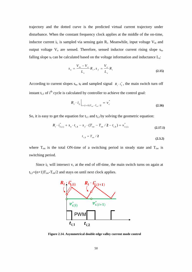
50
trajectory and the dotted curve is the predicted virtual current trajectory under
disturbance. When the constant frequency clock applies at the middle of the on-time,
inductor current iL is sampled via sensing gain Ri. Meanwhile, input voltage Vin and
output voltage Vo are sensed. Therefore, sensed inductor current rising slope sn,
falling slope sf can be calculated based on the voltage information and inductance Ls:
i
s
o
fi
s
oin
nR
L
VsR
L
VVs
,
(2.15)
According to current slopes sn, sf and sampled signal *
LiiR , the main switch turn off
instant ti,1 of ith
cycle is calculated by controller to achieve the control goal:
*
/)(c
TTitLi
viRonsw
21
(2.16)
So, it is easy to get the equation for ti,1 and ti,2 by solving the geometric equation:
)(
*
,,)(
*)/(
icionswfiniLivtTTstsiR
112
(2.17.1)
22
/, oni
Tt (2.3.2)
where Ton is the total ON-time of a switching period in steady state and Tsw is
switching period.
Since iL will intersect vc at the end of off-time, the main switch turns on again at
ti,2=(n+1)Tsw-Ton/2 and stays on until next clock applies.
Figure 2.14. Asymmetrical double edge valley current mode control

51
2.6.2 Small-Signal Model using Describing Function Method
A. Model Derivation
Appling the predictive algorithm, the controller decides the switching instant as if
the current is continuously sensed by sensing gain Ri. Since this virtual current feeds
back not only the modulation frequency fm, but also the sideband frequency N∙fsw±fm,
closed current feedback loop is a highly dynamic non-linear loop, so the closed
current loop has to be treated as an entity [E2] and modeled by describing function
(DF) method to include all the sideband frequency effect. The situation of voltage
loop is simpler since the low pass filter of the power stage and the low pass filter in
voltage loop compensator well attenuate the sideband frequency components, so only
perturbation frequency component is considered in voltage loop.
Referring to Figure 2.13, for modeling purpose, the voltage loop is broken and a
small magnitude sinusoidal perturbation vc at frequency fm is injected into the control
signal vc. The perturbation signal is )sin(ˆ)( tfrrtvmc
20
, where r0 is the
steady-state value of the control signal, r̂ is the magnitude of the signal, and θ is
the initial angle. Sampled control signal vc* updates at the beginning of each
switching cycle. Describing function from the control signal vc to the inductor current
iL can be found. It is necessary to make several assumptions: 1) the current slope sn
and sf are constant; 2) the magnitude of the perturbation signal is very small; 3) the
perturbation frequency fm and the switching frequency fsw are commensurable:
swmfNfM . 4) The quantization error is negligible in proper design. Assume ADC
finishes conversion instantaneously, based on the modulation law, it is found that:
)()()()(),(),( ic
on
ionswfionn
on
nictv
TTTsTs
Tstv
22
111
(2.18)
where TON(i,1) is the first on time interval of ith
cycle ON-time. Assume
TON(i,1)=TON/2+ΔTON(i,1), where ΔTON(i,1) is the ith
cycle On-time perturbation,
then:

52
)()()(),( 11
icicionfn
tvtvTss
(2.19)
The perturbed duty cycle d(t) and the inductor current iL (t) are expressed by
(2.20) and (2.21):
)]()()([)(),(),( 2
1
10 ioni
M
i
ioniiMTtTttuTttuttutd
sw
(2.20)
0
00
1L
t
fnMTtLidttdstdsti
sw
)]([)()(
(2.21)
Based on (2.20) and (2.21), Fourier analysis is performed on the inductor current
to obtain the Fourier coefficient iL(fm) at perturbation frequency:
dtetiN
fc
swm
MTtfj
L
m
m
0
2)(
(2.22)
where cm is the Fourier coefficient at perturbation frequency fm.
The Fourier coefficient at perturbation frequency fm for the control signal vc(t) is
jerj
2/ˆ
; therefore, the Describing Function from vc to iL can be calculated:
22
2
21
on
mswm
m
m
Tfj
ms
inTfj
fn
sw
fc
fLe
fjL
Ve
ss
f
v
i
)(
)(
)(
(2.23)
The transfer function in the s-domain can be expressed as follows:
21
on
sw
Ts
s
inTs
fn
sw
c
L esL
Ve
ss
f
sv
si
)()(
)(
(2.24)
Using the Pade approximation (2.25), the exponential term is approximated by
second order polynomial, which is valid up to half of switching frequency:
2
212
1
11
)(
s
Q
se swTs
where
212 Q
Tsw
,
(2.25)

53
The simplified s-domain control-to-inductor current transfer function is (2.26). As
shown in Figure.2.15, the model (2.26) well matches with simulation result up to half
of switching frequency.
Figure 2.15. Perturbed inductor current waveform
2
2
212
1
11onT
s
ic
L es
Q
sRsv
si
)()(
)(
(2.26)
In (2.26), 1/Ri is the low frequency current control gain, while the second order
term represents the non-ideality of current control----a pair of double poles at half
switching frequency. With this modulation, the double poles are always at left half
plane with quality factor /2Q (ξ≈0.7). Unlike analog valley current mode control,
the current loop of asymmetrical double edge valley current mode control is always
stable with proper damping. The exponential term represents the time delay between
update of vc* and control action. The analysis for iL(s)/vc(s) is applicable to any other
power converters since the inductor current loop and PWM switch are the common
sub-circuit.
For a Buck converter, it is straight forward to derive the vo(s)/vc(s) transfer
function:

54
2
2
212
1
1
1
1onT
s
oCoL
oCo
i
L
c
o es
Q
ssCRR
sCR
R
R
sv
sv
)()()(
)(
(2.27)
where RCo is the ESR of the output capacitors, Co is the capacitance of the output
capacitors.
Assuming the output filter and the low pass filter of the voltage compensator well
attenuate the sideband frequency components of output voltage, it is reasonable to
consider only the modulation frequency fm in voltage feedback loop. Without the
complication due to the sideband effect, the sampler at vc perturbation injection path
and vo feedback path can be modeled by the same transfer function swsam
TsG /)( 1 ,
so transfer function between sampled output voltage vo*(s) and control signal vc
*(s) is:
2
2
212
1
1
1
1 on
c
o
Ts
oCoL
oCo
i
L
samc
samo
es
Q
ssCRR
sCR
R
R
sGsv
sGsv
sv
sv
)()(
)()(
)()(
)(
)(
*
*
(2.28)
In practical implementation, Analog-to-Digital conversion may not finish before
turn off instant ti,1. Also, the digital controller calculation time adds to this time delay.
In this case, the updated information can only be use in the following switching
period. Generally, assume the delay time is td, then the sampled current information is
used to determine the duty cycle of the Kth
switching period after the sampling, where
K is express by (2.29), where floor is downward truncates function:
]/)/[(swond
TTtfloorK 2 (2.29)
Including conversion time delay, the time domain equation (2.18) becomes:
)()/()/()(),(),( iconKionswfKionnonnic
tvTTTsTsTstv
22111
(2.30)

55
Figure 2.16. Transfer Function iL(s)/vc(s) (D=0.1)
Similar to the derivation from (2.19)-(2.26), including the delay time, the transfer
function from control-to-iL is:
)(
)()(
)( swon
TKT
s
ic
Le
s
Q
sRsv
si
2
2
212
1
11
where
212 Q
Tsw
,
(2.31)
For Buck converter, the v*
o(s)/v*
c(s) transfer function is:
)(
*
*
)()()(
)( swon
c
oTK
Ts
oCoL
oCo
i
Le
s
Q
ssCRR
sCR
R
R
sv
sv
2
2
212
1
1
1
1
(2.32)
B. Model Extension to other schemes
The proposed model can be used for other of predictive current mode control,
including peak current mode control, valley current mode control and average current
mode control with leading edge modulation, trailing edge modulation and symmetric

56
double edge modulation and asymmetric double edge modulation [E9][E11][E12].
The sub-harmonic instability of each modulation is predicted by the proposed model.
Generally, the control-to-iL transfer function is expressed by (2.33), where Q is
the quality factor of the double poles at half of switching frequency, and Tx is the
delay time caused by the time interval between information sampling and switching
action. K is still defined as the number of delaying switching cycle caused by the
ADC conversion time and controller calculation time.
)(
)()(
)(swx TKTs
ic
L es
Q
sRsv
si
2
22
1
11
(2.33)
For Buck converter, the v*
o(s)/v*
c(s) transfer function is:
)(
*
*
)()()(
)(swx
c
o TKTs
oCoL
oCo
i
Le
s
Q
ssCRR
sCR
R
R
sv
sv
2
212
1
1
1
1
(2.34)
The results of Q and Tx are summarized in Table 2.3.
C. Model Extension to Multi-sampled Predictive Current Control and the
comparison with conventional Z-domain model
In previous section, the analysis is based on the single sample implementation.
Multi-sampled PWM can improve the converter transient performance and reduce
steady state output error [E22]. The proposed model is extended to multi-sampled
case in this section. The derivation is similar to the derivation for single sample
implementation. Assuming AD conversion time and calculation time are negligible,
the control-to-iL transfer function is expressed by (2.35), where the Txm represents the
delay time caused by the time interval between information sampling and switching
action. Txm for different modulations are listed in Table 2.4. It is found that
multi-sampling does not change the current loop stability but reduce delay in
vc*(s)/vo
*(s), so Q values are the same as that of single sample implementations in
Table 2.3.
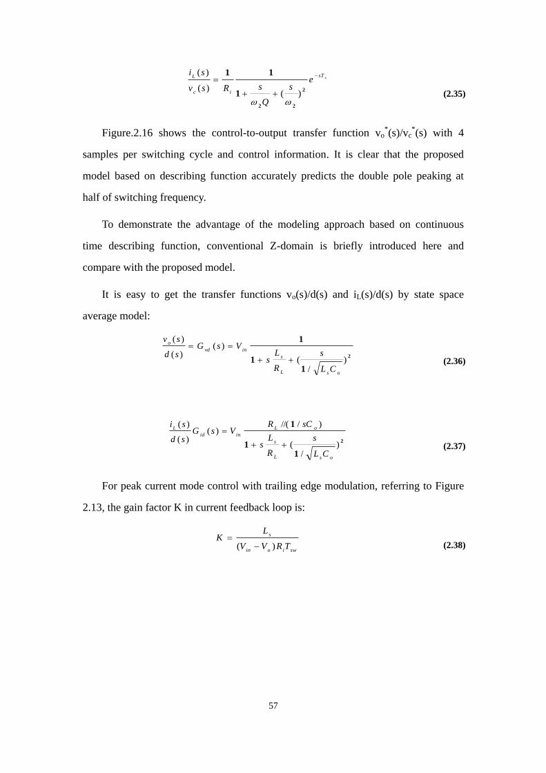
57
xsT
ic
Le
s
Q
sRsv
si
2
22
1
11
)()(
)(
(2.35)
Figure.2.16 shows the control-to-output transfer function vo*(s)/vc
*(s) with 4
samples per switching cycle and control information. It is clear that the proposed
model based on describing function accurately predicts the double pole peaking at
half of switching frequency.
To demonstrate the advantage of the modeling approach based on continuous
time describing function, conventional Z-domain is briefly introduced here and
compare with the proposed model.
It is easy to get the transfer functions vo(s)/d(s) and iL(s)/d(s) by state space
average model:
2
11
1
)/
(
)()(
)(
osL
s
invd
o
CL
s
R
Ls
VsGsd
sv
(2.36)
2
11
1
)/
(
)///()(
)(
)(
osL
s
oL
inid
L
CL
s
R
Ls
sCRVsG
sd
si
(2.37)
For peak current mode control with trailing edge modulation, referring to Figure
2.13, the gain factor K in current feedback loop is:
swioin
s
TRVV
LK
)(
(2.38)
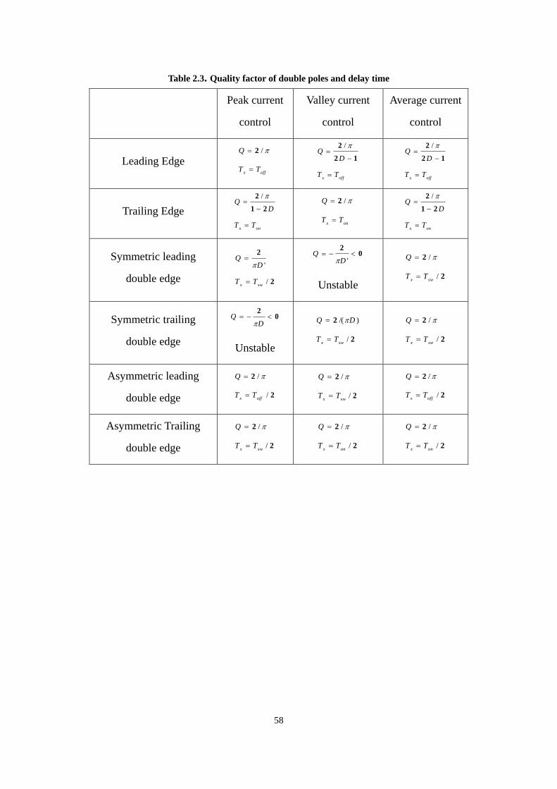
58
Table 2.3. Quality factor of double poles and delay time
Peak current
control
Valley current
control
Average current
control
Leading Edge offx
TT
Q
/2
offx
TT
DQ
12
2 /
offxTT
DQ
12
2 /
Trailing Edge
onxTT
DQ
21
2 /
onx
TT
Q
/2
onx
TT
DQ
21
2 /
Symmetric leading
double edge 2
2
/
'
swxTT
DQ
02
'D
Q
Unstable 2
2
/
/
swxTT
Q
Symmetric trailing
double edge
02
D
Q
Unstable 2
2
/
)/(
swxTT
DQ
2
2
/
/
swxTT
Q
Asymmetric leading
double edge 2
2
/
/
offxTT
Q
2
2
/
/
swxTT
Q
2
2
/
/
offxTT
Q
Asymmetric Trailing
double edge 2
2
/
/
swxTT
Q
2
2
/
/
onxTT
Q
2
2
/
/
onxTT
Q

59
Table 2.4. Delay time of each modulation law with N samples/Tsw
Delay time Tx
Leading Edge swoffxT
N
NDfloorTT
)'(
Trailing Edge swonxT
N
NDfloorTT
)(
Symmetric leading double edge sw
sw
xT
N
NDfloorTT
)/'( 2
2
Symmetric trailing double edge sw
sw
xT
N
NDfloorTT
)/( 2
2
Asymmetric Leading double edge sw
off
xT
N
NDfloorTT
)/'( 2
2
Asymmetric Trailing double edge sw
on
xT
N
NDfloorTT
)/( 2
2
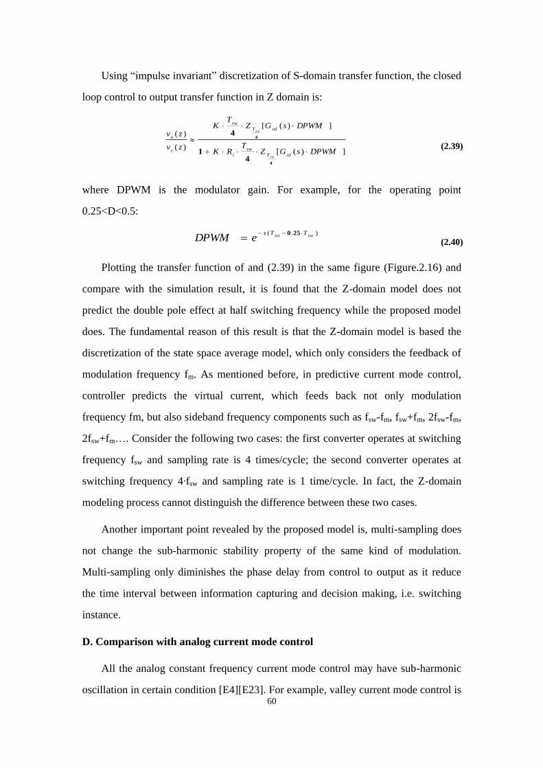
60
Using “impulse invariant” discretization of S-domain transfer function, the closed
loop control to output transfer function in Z domain is:
])([
])([
)(
)(
DPWMsGZT
RK
DPWMsGZT
K
zv
zv
idT
sw
i
vdT
sw
c
o
sw
sw
4
4
41
4
(2.39)
where DPWM is the modulator gain. For example, for the operating point
0.25<D<0.5:
).( swon TTseDPWM
250
(2.40)
Plotting the transfer function of and (2.39) in the same figure (Figure.2.16) and
compare with the simulation result, it is found that the Z-domain model does not
predict the double pole effect at half switching frequency while the proposed model
does. The fundamental reason of this result is that the Z-domain model is based the
discretization of the state space average model, which only considers the feedback of
modulation frequency fm. As mentioned before, in predictive current mode control,
controller predicts the virtual current, which feeds back not only modulation
frequency fm, but also sideband frequency components such as fsw-fm, fsw+fm, 2fsw-fm,
2fsw+fm…. Consider the following two cases: the first converter operates at switching
frequency fsw and sampling rate is 4 times/cycle; the second converter operates at
switching frequency 4∙fsw and sampling rate is 1 time/cycle. In fact, the Z-domain
modeling process cannot distinguish the difference between these two cases.
Another important point revealed by the proposed model is, multi-sampling does
not change the sub-harmonic stability property of the same kind of modulation.
Multi-sampling only diminishes the phase delay from control to output as it reduce
the time interval between information capturing and decision making, i.e. switching
instance.
D. Comparison with analog current mode control
All the analog constant frequency current mode control may have sub-harmonic
oscillation in certain condition [E4][E23]. For example, valley current mode control is

61
unstable for D<0.5 without external ramp. The fundamental reason is the
sample-and-hold effect of the current feedback, which introduce the double poles at
(1/2)fsw. To properly damp the current loop, an adaptive ramp has to be applied to
current loop according to duty cycle D [E2][E4]. The situation changes in digital
predictive control. The proper predicting logic (for example, asymmetrical double
edge valley current mode control) can eliminate the sample and hold effect for any
duty cycle. Current loop is always well-damped to damping ratio ξ≈0.7. Current
dynamic deviation settles down in one switching cycle. That is the advantage of
digital predictive implementation. The limitation of digital predictive current mode
control is the time delay between control signal update and switching action reduces
outer control bandwidth.
Figure 2.17. Simulation verification for vo*(s)/vc*(s) of Buck
( fsw=300kHz, Vin=12V, Vo=5V, Ls=300nH, Co=4800μF, RCo=0.75mΩ,
RL=0.1Ω, 4 sample/cycle)
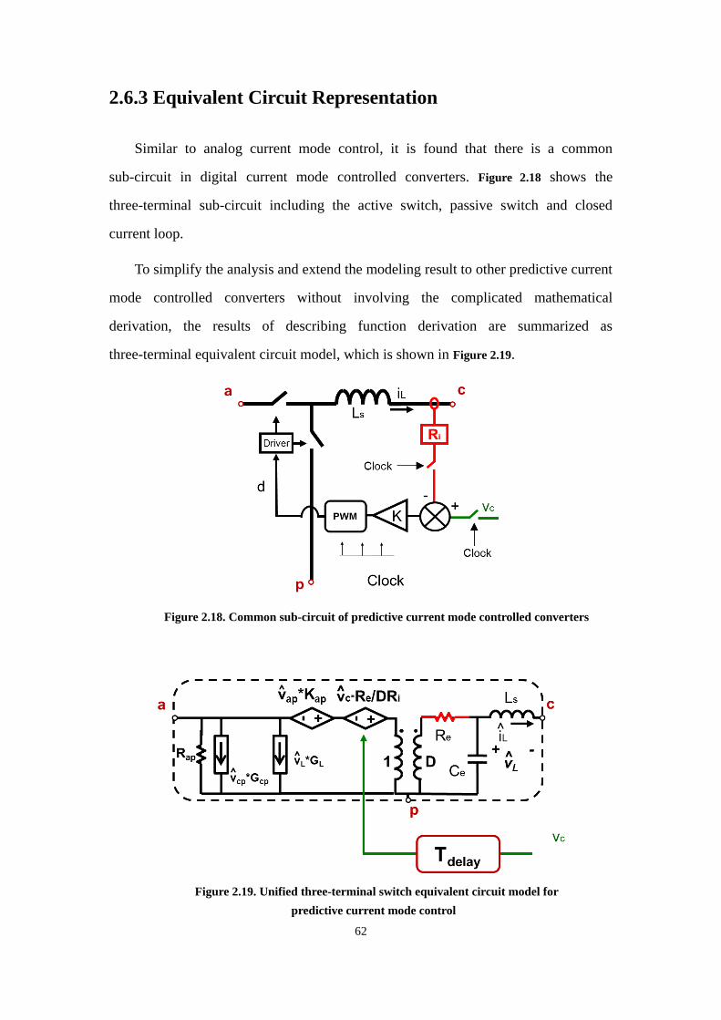
62
2.6.3 Equivalent Circuit Representation
Similar to analog current mode control, it is found that there is a common
sub-circuit in digital current mode controlled converters. Figure 2.18 shows the
three-terminal sub-circuit including the active switch, passive switch and closed
current loop.
To simplify the analysis and extend the modeling result to other predictive current
mode controlled converters without involving the complicated mathematical
derivation, the results of describing function derivation are summarized as
three-terminal equivalent circuit model, which is shown in Figure 2.19.
Figure 2.18. Common sub-circuit of predictive current mode controlled converters
Figure 2.19. Unified three-terminal switch equivalent circuit model for
predictive current mode control

63
In Figure 2.19, D is the steady state duty cycle and Ls is the power stage inductor.
Other parameters in the equivalent circuit are defined by:
ap
c
LV
IG
(2.41)
ap
c
cpV
IG
(2.42)
c
ap
apDI
VR
(2.43)
All the modulation laws discussed in this chapter are constant frequency
modulations, so the double poles are at half of the switching frequency. In the
equivalent circuit, the resonant of Ce and Ls form the double pole. Ce is defined by:
2
2
s
sw
eL
TC
(2.44)
Re represents the double pole damping effect. For some of the modulation laws,
the double pole can move to right-half-plane. In the equivalent circuit representation,
Re can be positive or negative in these control laws. When Re is negative, the current
loop in unstable.
Tdelay indicates the pure time delay between the last sampling point to the
switching action.
Table 2.5 lists the definition of Re, Ce and Tdelay for different modulation law and
control mode.
Figure 2.20 shows an example using the three-terminal equivalent circuit mode in
predictive current mode control Buck converter.
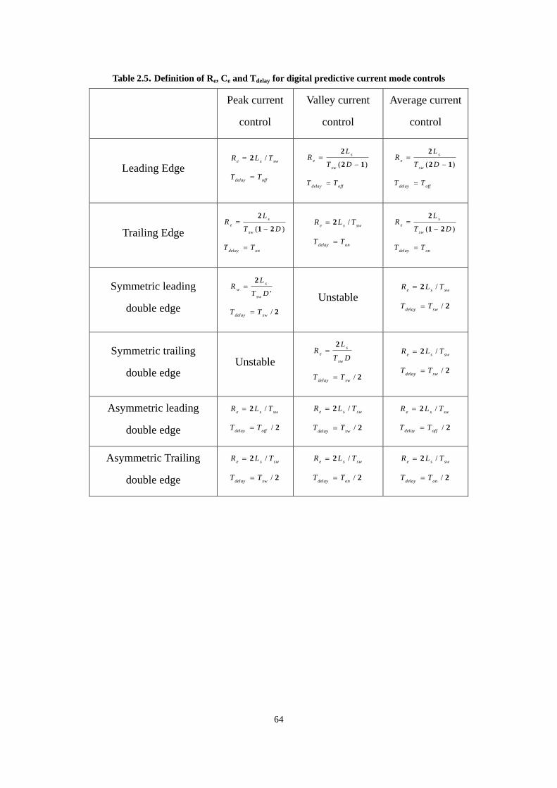
64
Table 2.5. Definition of Re, Ce and Tdelay for digital predictive current mode controls
Peak current
control
Valley current
control
Average current
control
Leading Edge offdelay
swse
TT
TLR
/2
offdelay
sw
s
e
TT
DT
LR
)( 12
2
offdelay
sw
s
e
TT
DT
LR
)( 12
2
Trailing Edge
ondelay
sw
s
e
TT
DT
LR
)( 21
2
ondelay
swse
TT
TLR
/2
ondelay
sw
s
e
TT
DT
LR
)( 21
2
Symmetric leading
double edge 2
2
/
'
swdelay
sw
s
w
TT
DT
LR
Unstable 2
2
/
/
swdelay
swse
TT
TLR
Symmetric trailing
double edge Unstable
2
2
/swdelay
sw
s
e
TT
DT
LR
2
2
/
/
swdelay
swse
TT
TLR
Asymmetric leading
double edge 2
2
/
/
offdelay
swse
TT
TLR
2
2
/
/
swdelay
swse
TT
TLR
2
2
/
/
offdelay
swse
TT
TLR
Asymmetric Trailing
double edge 2
2
/
/
swdelay
swse
TT
TLR
2
2
/
/
ondelay
swse
TT
TLR
2
2
/
/
ondelay
swse
TT
TLR

65
Figure 2.20. Equivalent circuit for predictive current mode control Buck converter
2.7 Verification of the Proposed Model
The proposed small signal model is verified in this section. The SIMPLIS
simulation tool is used to verify the proposed model.
2.7.1 Constant Frequency Modulation Current Mode Control
A. Peak current mode control Buck converter
The parameters of the peak current-mode control buck converter are as follows:
Vin = 12V, Vo = 5V, fs = 300KHz, Co = 8×560μF, RCo = 6/8mΩ, and Ls =300nH. The
control-to-output transfer function and the audio susceptibility are shown in Figure 2.21
while input and output impedance comparisons are shown and Figure 2.22. The
proposed model can accurately predict the system response up to half of the switching
frequency.

66
Figure 2.21. Simulation verification of control-to-output and input-to-output
transfer function for peak current mode control Buck converter
Figure 2.22. Simulation verification of output impedance and input
impedance for peak current mode control Buck converter
B. Peak current mode control Boost converter
The circuit diagram and the small signal equivalent circuit of the Boost converter
are shown in Figure 2.23. The parameters of the peak current-mode control Boost

67
converter are as follows: Vin=220V, Vo=400V, RL=150Ω, fsw=100kHz, Ls=300μH,
ESR=3mΩ. The control-to-output transfer function and the audio susceptibility are
shown in Figure 2.24 while the input and output impedance comparisons are shown in
Figure 2.25. The proposed model can accurately predict the system response up to half
of the switching frequency.
Figure 2.23. Peak current mode control Boost converter and its small signal equivalent circuit
Figure 2.24. Simulation verification of control-to-output and input-to-output transfer function
for peak current mode control Boost converter

68
Figure 2.25. Simulation verification of output impedance and input impedance for peak
current mode control Boost converter
C. Charge control Flyback converter
The circuit diagram and small signal equivalent circuit of the Flyback converter
are shown in Figure 2.26. The parameters of the charge control Flyback converter are as
follows: Vin=500V, Vo=400V, RL=150Ω, fsw=100kHz, Ls=300μH, ESR=3mΩ. The
control to input current transfer function and the control to output are shown in Figure
2.27. The proposed model can accurately predict the system response up to half of the
switching frequency. As the purpose of charge control, the control to input current
transfer function is a flat gain up to half of the switching frequency.

69
Figure 2.26. Charge controlled Flyback converter and its small signal equivalent circuit
Figure 2.27. Simulation verification of control-to-input current and control-to-output
transfer function for charge control Flyback converter
2.7.2 Variable Frequency Modulation Current Mode Control
The SIMPLIS simulation tool is used to verify the proposed model for constant
on-time current-mode control. The parameters of the buck converter are as follows:

70
Vin=12V, Vo=1.2V, RL=100mΩ, Ton=333nS, Co = 8×560μF, RCo = 6/8mΩ, and
Ls=300nH. The control-to-output transfer function and the audio susceptibility are
shown in Figure 2.28 while input and output impedance comparisons are shown in
Figure 2.29. The proposed model can accurately predict the system response.
Figure 2.28. Simulation verification of control-to-output and input-to-output transfer
function for constant on-time current mode control Buck converter
2.8 Summary
This chapter presents a unified three-terminal switch model for current mode
controls. Based on the observation, the PWM switch and the closed current loop is
taken as an invariant sub-circuit which is common to different DC/DC converter
topologies. The basic small signal relationship is studied and the result shows that the
PWM switch with current feedback preserve the property of PWM switch. A
three-terminal equivalent circuit is developed to represent the small signal behavior of
this common sub-circuit. The proposed model is a unified model that is applicable in
both constant frequency modulation and variable frequency modulation. The physical
meaning of the three-terminal equivalent circuit model is discussed. The model are
verified by SIMPLIS simulation in commonly used converters for both constant

71
frequency modulation and variable frequency modulation.
Figure 2.29. Simulation verification of input impedance and output impedance for constant
on-time current mode control Buck converter

72
Chapter 3. Extend Equivalent Circuit to Average
Current Mode Control and Design Guideline
A small signal model for average current mode control based on equivalent
circuit is proposed. The model uses the three-terminal equivalent circuit model based
on linearized describing function method to include the feedback effect of the
side-band frequency components of inductor current. It extends the results obtained in
peak-current model control to average current mode control. The proposed small
signal model is accurate up to half switching frequency, predicting the sub-harmonic
instability. The proposed model is verified using SIMPLIS simulation and hardware
experiments, showing good agreement with the measurement results. Based on the
proposed model, a new feedback design guideline is presented. The proposed design
guideline is compared with several conventional, widely used design criteria to
highlight its virtue. By designing the external ramp following the proposed design
guideline, quality factor of the double poles at half of switching frequency in
control-to-output transfer function can be precisely controlled. This helps the
feedback design to achieve widest control bandwidth and proper damping.
3.1 Introduction
Average current mode control [B1] is widely used in many applications, such as
power factor correction, point-of-load converter, battery charger and LED driver. Due
to the popularity of current-mode control, an accurate model for current-mode control
is indispensable to system design. Figure 3.1 shows an average current mode controlled
Buck converter.
The small signal model of average current mode control has been studied for
more than two decades. Essentially, PWM converter is a nonlinear circuit. Under a
single frequency fm perturbation injection, state variable iL contains all the sideband
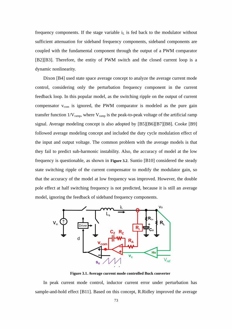
73
frequency components. If the stage variable iL is fed back to the modulator without
sufficient attenuation for sideband frequency components, sideband components are
coupled with the fundamental component through the output of a PWM comparator
[B2][B3]. Therefore, the entity of PWM switch and the closed current loop is a
dynamic nonlinearity.
Dixon [B4] used state space average concept to analyze the average current mode
control, considering only the perturbation frequency component in the current
feedback loop. In this popular model, as the switching ripple on the output of current
compensator vcom is ignored, the PWM comparator is modeled as the pure gain
transfer function 1/Vramp, where Vramp is the peak-to-peak voltage of the artificial ramp
signal. Average modeling concept is also adopted by [B5][B6][B7][B8]. Cooke [B9]
followed average modeling concept and included the duty cycle modulation effect of
the input and output voltage. The common problem with the average models is that
they fail to predict sub-harmonic instability. Also, the accuracy of model at the low
frequency is questionable, as shown in Figure 3.2. Suntio [B10] considered the steady
state switching ripple of the current compensator to modify the modulator gain, so
that the accuracy of the model at low frequency was improved. However, the double
pole effect at half switching frequency is not predicted, because it is still an average
model, ignoring the feedback of sideband frequency components.
Figure 3.1. Average current mode controlled Buck converter
In peak current mode control, inductor current error under perturbation has
sample-and-hold effect [B11]. Based on this concept, R.Ridley improved the average

74
model of peak current mode control by inserting a pair of right-half-plan double zero
He(s) in the current feedback path [B12]. This model well predicts the sub-harmonic
instability of peak current mode control. Tang tried to consider nonlinearity of the
current loop of average current mode control and gave a small signal model in [B13].
This model assumed that the same sample-and-hold effect also exists in average
current mode control and inherited the He(s) term in the current feedback path without
solid justification. The modulator gain Fm was derived in [B13] considering the
switching ripple of vcom but the result is not consistent with Fm in peak current mode
control [B12] when the compensator is degenerated to a pure gain. Moreover, it is
unreasonable to assume the current compensator has different transfer function in
voltage loop and current loop. Due to these debatable assumptions, the accuracy of
this model is questionable. Some other literatures, such as [B14] and [B15], claimed
the current loop has two sampler but the models were not justified. Figure 3.2
compares the simulation result with models [B4][B9][B13], which shows that the
validation of these models are not satisfactory.
Figure 3.2. Control-to-iL transfer function comparison (Vin=12V, Vo=5V,
Ls=300nH, Co=3mF, Rz=20kΩ, RA=1kΩ, Cz=100nF, RL=0.5Ω, se=2V)
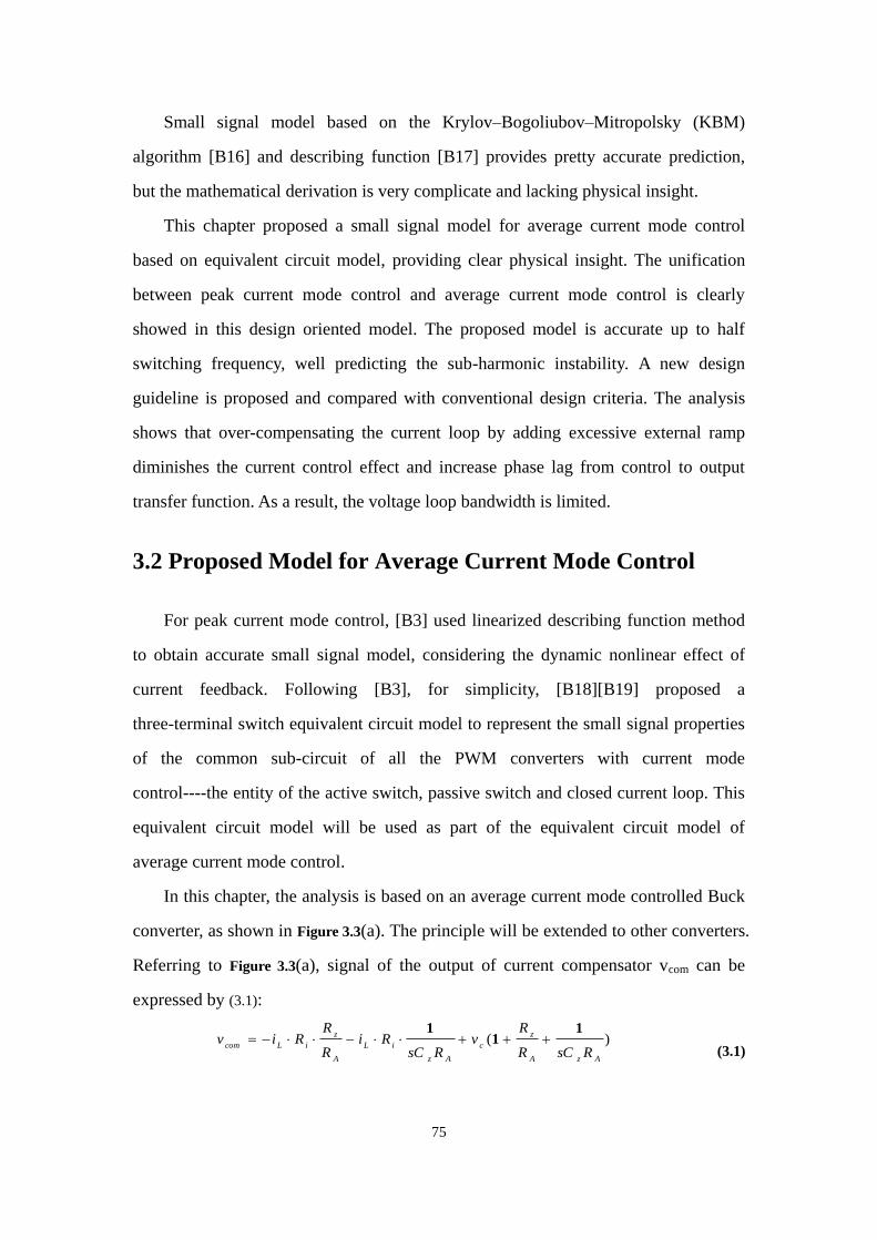
75
Small signal model based on the Krylov–Bogoliubov–Mitropolsky (KBM)
algorithm [B16] and describing function [B17] provides pretty accurate prediction,
but the mathematical derivation is very complicate and lacking physical insight.
This chapter proposed a small signal model for average current mode control
based on equivalent circuit model, providing clear physical insight. The unification
between peak current mode control and average current mode control is clearly
showed in this design oriented model. The proposed model is accurate up to half
switching frequency, well predicting the sub-harmonic instability. A new design
guideline is proposed and compared with conventional design criteria. The analysis
shows that over-compensating the current loop by adding excessive external ramp
diminishes the current control effect and increase phase lag from control to output
transfer function. As a result, the voltage loop bandwidth is limited.
3.2 Proposed Model for Average Current Mode Control
For peak current mode control, [B3] used linearized describing function method
to obtain accurate small signal model, considering the dynamic nonlinear effect of
current feedback. Following [B3], for simplicity, [B18][B19] proposed a
three-terminal switch equivalent circuit model to represent the small signal properties
of the common sub-circuit of all the PWM converters with current mode
control----the entity of the active switch, passive switch and closed current loop. This
equivalent circuit model will be used as part of the equivalent circuit model of
average current mode control.
In this chapter, the analysis is based on an average current mode controlled Buck
converter, as shown in Figure 3.3(a). The principle will be extended to other converters.
Referring to Figure 3.3(a), signal of the output of current compensator vcom can be
expressed by (3.1):
)(
AzA
z
c
Az
iL
A
z
iLcomRsCR
Rv
RsCRi
R
RRiv
11
1
(3.1)

76
The first term of (3.1) is the proportional feedback of the inductor current iL, while
other terms represent the integration of the error between inductor current and control
signal vc. Proportional feedback contains all the sideband frequency components. For
practical design, as illustrated in Figure 3.4, since the zero of the current compensator
is well below switching frequency, so the gain of integration term is much smaller
than the proportional term at f>(1/2)fsw. Also, due to the low pass filters of power
stage and voltage compensator, the sideband frequency of vc is well attenuated. As a
result, only the first term of (3.1) contributed the majority of the sideband components,
causing the nonlinearity of the control loop, whereas it is reasonable to consider only
the fundamental frequency for the second term and third term.
In the light of this understanding, for modeling purpose, the diagram of average
current mode control is redrawn as Figure 3.3(b). In this alternative representation,
there are two current feedback loops. The inner loop corresponding to the
proportional feedback term and the outer current loop represents the integration part.
It is easy to find that the inner loop is the same as peak current mode control.
Substituting the inner loop and the switches with the three-terminal switch model
[B18][B19], the equivalent circuit model of average current mode control is obtained,
as shown in Figure 3.5. In the equivalent circuit, equivalent current sensing gain is Ri’:
A
z
iiR
RRR
(3.2)
Solving the linear equivalent circuit Figure 3.5, designer can obtain any transfer
function of interest. More analysis and discussion on the dynamic model are presented
in next section.
To demonstrate the accuracy of this model and the improvement over the
conventional models, Figure 3.6 shows the control to iL transfer function. As shown in
Figure 3.6, the proposed model well predicts the SIMPLIS simulation result. The
proposed model has better accuracy than the conventional models [B4] and [B13].

77
Figure 3.3. Separation of current feedback information
Figure 3.4. Comparison of the gain of integration and proportional term
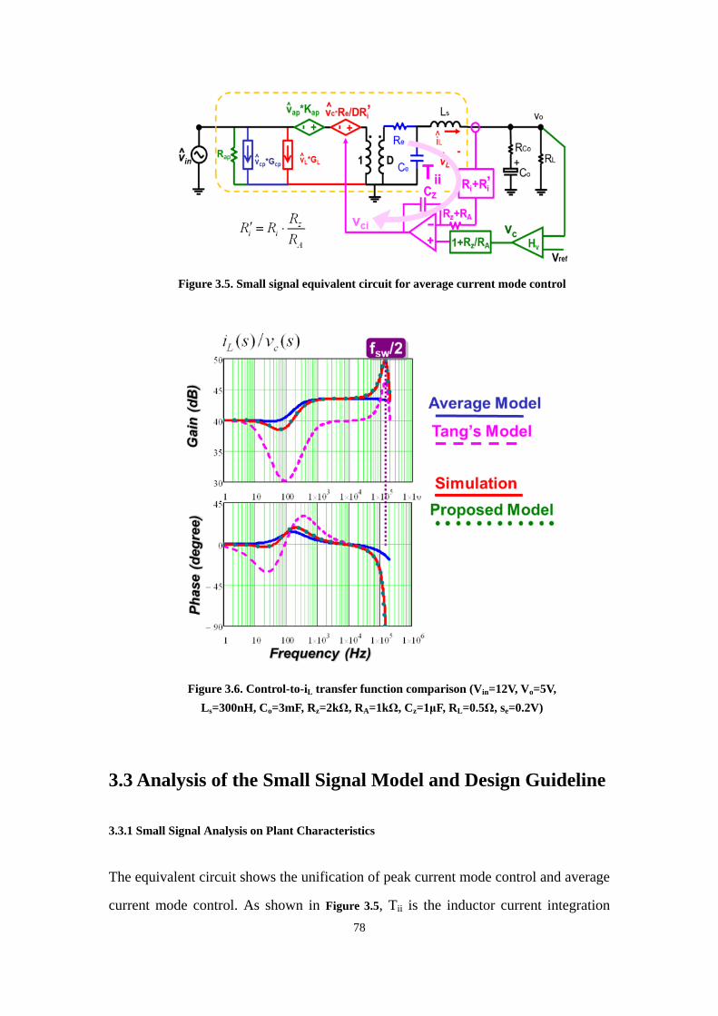
78
Figure 3.5. Small signal equivalent circuit for average current mode control
Figure 3.6. Control-to-iL transfer function comparison (Vin=12V, Vo=5V,
Ls=300nH, Co=3mF, Rz=2kΩ, RA=1kΩ, Cz=1μF, RL=0.5Ω, se=0.2V)
3.3 Analysis of the Small Signal Model and Design Guideline
3.3.1 Small Signal Analysis on Plant Characteristics
The equivalent circuit shows the unification of peak current mode control and average
current mode control. As shown in Figure 3.5, Tii is the inductor current integration

79
loop. As an extreme case, when Cz is infinity, the integration loop is essentially
opened. The open loop control to inductor current transfer function exhibits the
characteristic of peak current mode control:
2
2
2
221
1
1
1
/)/()||()(
)(
sQssCRR
sCRG
sv
si
oeL
oL
ci
Cc
L
z
where Le
e
Azzi
ciRR
R
RRRRG
)]/([
1
swesTCL /)/( 21
2
(3.3)
The double pole of (3.3) is at half of switching frequency and the quality factor Q2
indicates the sub-harmonic stability. Q2 is defined by (3.4), where snc sfc are rising
slope, falling slope of amplified sensed inductor current signal at the output of current
compensator. The equivalent current sensing gain is Ri’ while se is external ramp slope
on the PWM comparator:
]}.)/()[(/{ 5012
fcncenc
ssssQ
where s
oin
incL
VVRs
' ,
s
o
ifcL
VRs ' ,
A
z
iiR
RRR '
(3.4)
For Buck converter, it is easy to derive the control-to-output transfer function:
2
2
2
221
1
1
1
/)/()||()(
)(
sQssCRR
sCRG
sv
sv
oeL
oCo
cv
Cc
o
z
where Le
e
Azzi
L
cvRR
R
RRRR
RG
)]/([
(3.5)
As the Cz decreases from infinity, the crossover frequency of the integration loop
Tii increases from zero, then the dynamic characteristic of average current mode
control gradually deviates from peak current mode control, showing the control-to-iL
gain correcting effect of the integration loop. Figure 3.7 shows the transition between
average current mode control and peak current mode control, using control to iL
transfer function as an example.
80
3.3.2 Compensation Design Guideline
The target of designing the current compensator is to shape the
control-to-inductor current transfer function to be a flat gain up to highest possible
frequency, i.e. half of switching frequency, minimize the phase delay, and avoid the
double pole peaking at half of switching frequency.
1) Place the zero based on integration loop gain
The goal of integration function is to eliminate the current control error of peak
current mode control at low frequency. In another word, the goal of average current
mode control is to achieve constant gain between vc and iL.
The pole-zero pair of the plant cause the gain deviation at low frequency, as
shown in Figure 3.7. In order to correct the gain, the integration loop Tii crossover
frequency must be above the pole frequency fp:
])||(/[oeLp
CRRf 21
(3.6)
It can be proved that the cross over frequency of Tii is the the frequency of the
zero of the current compensator, so the zero should be placed above fp:
pzzzerofRCf )/( 21
(3.7)
To guarantee enough phase margin, the zero is suggested to be well below half of
switching frequency, for example, one tenth of switching frequency. If the design
violate requirement (3.6), flat control to inductor current gain cannot be achieved. This
point was not reported in conventional design guidelines, such as [B4][B9][B13]. If
the requirement (3.6) is met, the closed loop control to iL transfer function is:
2
2
2
221
1
1
11
/)/(
)(
)(
)(
sQssCR
sCRR
Rsv
si
zz
zzA
ic
L
(3.8)
In (3.8), the low frequency pole and zero of the plant is wiped out by the control
loop. The new pole and zero is determined by controller.

81
2) Select the RC components
Based on (3.8), the low frequency pole and zero is determined by controller. To
get a flat gain, we need to make the pole and zero to be close so that the effects are
cancelled by each other. Rz should be much larger than RA, for example, Rz=10∙RA.
Larger ratio between Rz and RA is good from small signal point of view, but it may
require a high gain-bandwidth product operation amplifier in implementation.
Figure 3.7. Transition between average current
mode control and peak current mode control
3) Design external ramp compensation
Following the design guideline, the control to iL transfer function has a flat gain
within half switching frequency. The control to iL transfer function and control to
output transfer function become very simple:
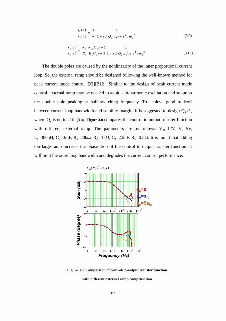
82
2
2
2
221
11
/)/()(
)(
sQsRsv
si
ic
L
(3.9)
2
2
2
221
1
1
1
/)/()(
)(
sQssCR
sCR
R
R
sv
sv
oL
oCo
i
L
c
o
(3.10)
The double poles are caused by the nonlinearity of the inner proportional current
loop. So, the external ramp should be designed following the well-known method for
peak current mode control [B3][B12]. Similar to the design of peak current mode
control, external ramp may be needed to avoid sub-harmonic oscillation and suppress
the double pole peaking at half switching frequency. To achieve good tradeoff
between current loop bandwidth and stability margin, it is suggested to design Q2≈1,
where Q2 is defined in (3.4). Figure 3.8 compares the control to output transfer function
with different external ramp. The parameters are as follows: Vin=12V, Vo=5V,
Ls=300nH, Co=3mF, Rz=20kΩ, RA=1kΩ, Cz=2.5nF, RL=0.5Ω. It is found that adding
too large ramp increase the phase drop of the control to output transfer function. It
will limit the outer loop bandwidth and degrades the current control performance.
Figure 3.8. Comparison of control-to-output transfer function
with different external ramp compensation
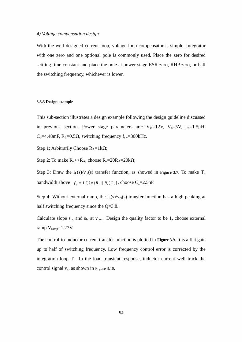
83
4) Voltage compensation design
With the well designed current loop, voltage loop compensator is simple. Integrator
with one zero and one optional pole is commonly used. Place the zero for desired
settling time constant and place the pole at power stage ESR zero, RHP zero, or half
the switching frequency, whichever is lower.
3.3.3 Design example
This sub-section illustrates a design example following the design guideline discussed
in previous section. Power stage parameters are: Vin=12V, Vo=5V, Ls=1.5μH,
Co=4.48mF, RL=0.5Ω, switching frequency fsw=300kHz.
Step 1: Arbitrarily Choose RA=1kΩ;
Step 2: To make Rz>>RA, choose Rz=20RA=20kΩ;
Step 3: Draw the iL(s)/vci(s) transfer function, as showed in Figure 3.7. To make Tii
bandwidth above ])||(/[oeLp
CRRf 21 , choose Cz=2.5nF.
Step 4: Without external ramp, the iL(s)/vci(s) transfer function has a high peaking at
half switching frequency since the Q=3.8.
Calculate slope snc and sfc at vcom. Design the quality factor to be 1, choose external
ramp Vramp=1.27V.
The control-to-inductor current transfer function is plotted in Figure 3.9. It is a flat gain
up to half of switching frequency. Low frequency control error is corrected by the
integration loop Tii. In the load transient response, inductor current well track the
control signal vc, as shown in Figure 3.10.

84
Figure 3.9. Design example of average current mode control
Figure 3.10. Simulation waveform for load transient response
3.3.4 Comparison with conventional design
Comparing with conventional design guideline [B4][B9][B13], the proposed
design approach enables a precise evaluation of compensator parameters, high current
loop bandwidth and exact specification of the damping of the double poles at half of
the switching frequency. Frequency range of compensation zero for proper design is
proposed. The external ramp is taken as a design parameter and the optimization is
discussed. For small duty cycle operation (i.e. D<0.3), no external ramp is needed to
achieve a well damped wide bandwidth current control.
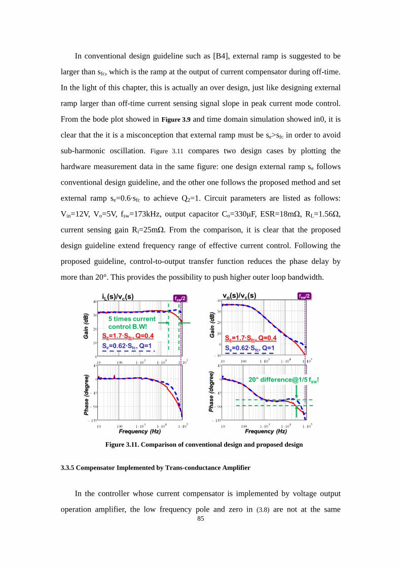
85
In conventional design guideline such as [B4], external ramp is suggested to be
larger than sfc, which is the ramp at the output of current compensator during off-time.
In the light of this chapter, this is actually an over design, just like designing external
ramp larger than off-time current sensing signal slope in peak current mode control.
From the bode plot showed in Figure 3.9 and time domain simulation showed in0, it is
clear that the it is a misconception that external ramp must be se>sfc in order to avoid
sub-harmonic oscillation. Figure 3.11 compares two design cases by plotting the
hardware measurement data in the same figure: one design external ramp se follows
conventional design guideline, and the other one follows the proposed method and set
external ramp se=0.6∙sfc to achieve Q2=1. Circuit parameters are listed as follows:
Vin=12V, Vo=5V, fsw=173kHz, output capacitor Co=330μF, ESR=18mΩ, RL=1.56Ω,
current sensing gain Ri=25mΩ. From the comparison, it is clear that the proposed
design guideline extend frequency range of effective current control. Following the
proposed guideline, control-to-output transfer function reduces the phase delay by
more than 20°. This provides the possibility to push higher outer loop bandwidth.
Figure 3.11. Comparison of conventional design and proposed design
3.3.5 Compensator Implemented by Trans-conductance Amplifier
In the controller whose current compensator is implemented by voltage output
operation amplifier, the low frequency pole and zero in (3.8) are not at the same

86
frequency. The reason is the transfer functions from inverting input iL∙Ri and
non-inverting input vc to the amplifier output vcom is different. For the controller
whose current compensator is implemented by trans-conductance amplifier, as shown
in Figure 3.12, since these transfer functions are identical, it is straight forward to find
that the pole and zero are cancelled. In this case, control to iL transfer function is:
2
2
2
221
11
/)/()(
)(
sQsRsv
si
ic
L
(3.11)
The quality factor Q2 is still defined by (3.3), whereas the equivalent current
sensing gain Ri’’ is (3.12), where gm is the trans-conductance of the amplifier:
zmiiRgRR ''
(3.12)
Figure 3.12. Average current mode controlled Buck converter with
Trans-conductance amplifier
3.4 Model Extension to Other Modulations
The modeling concept is discussed in previous sections based on constant
frequency trailing edge modulation. The proposed method can be extended to other
modulation schemes, such as constant frequency leading edge modulation, as well as
variable constant on-time modulation and constant off-time modulation. Using the
87
unified three terminal switch models for current mode controls of corresponding
modulation [B18][B19], the equivalent circuits of average current mode controls in
the form of Figure 3.5 are easily obtained. For variable frequency modulations, as the
inner current loop is inherently stable, no ramp is needed to stabilize the current loop
as long as the zero of the current compensator is well below half of switching
frequency.
3.5 The Analysis of Other Converters with Average Current
Mode Control
The equivalent circuit model can be applied to other converters with average
current mode control. The three-terminal switch with the integration loop Tii is the
common sub-circuit for average current mode controlled converters.
Figure 3.13 is the example of average current mode controlled Boost converter and
its equivalent circuit model.
For Boost converter, the signal slope snc and sfc is defined by:
s
in
incL
VRs '
(3.13)
s
ino
ifcL
VVRs
'
(3.14)
Similarly, for Buck-Boost converter, the signal slope snc and sfc is defined by:
s
in
incL
VRs '
(3.15)
s
o
ifcL
VRs '
(3.16)
The design guidelines for current compensator are the same as Buck converter.
3.6 Simulation and Experimental Verification
Figure 3.14 shows control-to-iL and control-to-output transfer function of Buck

88
converter respectively for a Buck converter with average current mode control.
Current amplifier is implemented by voltage amplifier. In the experiment, Vin=12V,
Vo=5V, fsw=173kHz, Ls=15μH, Bulk capacitor Co=330μF, ESR=18mΩ, RL=1.56Ω,
current sensing gain Ri=25mΩ, Vramp =1.2V. The experimental result is well predicted
by the proposed model up to half of switching frequency.
Figure 3.13. Average current mode controlled Boost converter
and its small signal equivalent circuit

89
Figure 3.14. Control-to-iL and control-to-output transfer function comparison
Figure 3.15 shows control-to-iL and control-to-output transfer function of Buck
converter respectively for a Buck converter with average current mode control.
Current amplifier is implemented by trans-conduction amplifier. In the experiment,
Vin=12V, Vo=3.3V, fsw=276kHz, Ls=600nH, Bulk capacitor Co=220μF, ESR=5mΩ,
RL=0.36Ω, current sensing gain Ri=34.5mΩ, Vramp =2V. The experimental result is
well predicted by the proposed model up to half of switching frequency.
Figure 3.15. Control-to-iL and control-to-output transfer function comparison

90
3.7 Conclusion
This chapter proposed a small signal model for average current mode control
based on describing function-based equivalent circuit. The model is verified to be
accurate up to half of switching frequency, which is better than popular conventional
models. A new design guideline is proposed, explicitly specifying the lowest
frequency for compensation zero, optimum ramp compensation and other constrains.
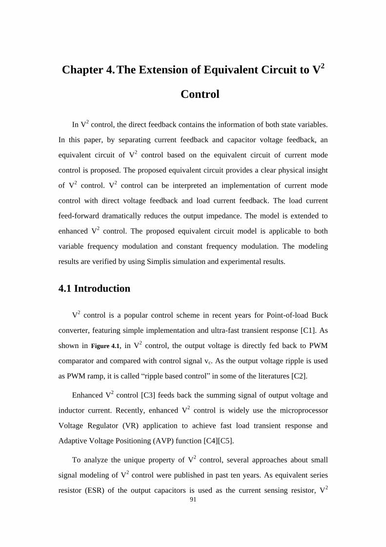
91
Chapter 4. The Extension of Equivalent Circuit to V2
Control
In V2 control, the direct feedback contains the information of both state variables.
In this paper, by separating current feedback and capacitor voltage feedback, an
equivalent circuit of V2 control based on the equivalent circuit of current mode
control is proposed. The proposed equivalent circuit provides a clear physical insight
of V2 control. V
2 control can be interpreted an implementation of current mode
control with direct voltage feedback and load current feedback. The load current
feed-forward dramatically reduces the output impedance. The model is extended to
enhanced V2 control. The proposed equivalent circuit model is applicable to both
variable frequency modulation and constant frequency modulation. The modeling
results are verified by using Simplis simulation and experimental results.
4.1 Introduction
V2 control is a popular control scheme in recent years for Point-of-load Buck
converter, featuring simple implementation and ultra-fast transient response [C1]. As
shown in Figure 4.1, in V2 control, the output voltage is directly fed back to PWM
comparator and compared with control signal vc. As the output voltage ripple is used
as PWM ramp, it is called “ripple based control” in some of the literatures [C2].
Enhanced V2 control [C3] feeds back the summing signal of output voltage and
inductor current. Recently, enhanced V2 control is widely use the microprocessor
Voltage Regulator (VR) application to achieve fast load transient response and
Adaptive Voltage Positioning (AVP) function [C4][C5].
To analyze the unique property of V2 control, several approaches about small
signal modeling of V2 control were published in past ten years. As equivalent series
resistor (ESR) of the output capacitors is used as the current sensing resistor, V2

92
control is consider as a special implementation of current mode control [C3][C6][C7].
[C3][C6][C7] borrowed the sample & hold concept of peak current mode control for
the analysis of constant frequency V2 control without justification, but the result is not
satisfactory. Paper [C7] even made a wrong conclusion that, with certain ESR, the
smaller capacitance increases the double pole damping effect at half of switching
frequency. More important, sample & hold concept is not applicable in variable
frequency modulation [C8], so the most popular constant on-time V2 control cannot
be analyzed based on this concept.
Figure 4.1 Constant On-time V2 Control
Small signal model based on describing function provides a good model for
control-to-output transfer function and output impedance in practical design range
[C9]. However, there are several unsettled issues in this model. First, the
mathematical derivation of this model is very complicated and time consuming. As a
result, small signal model of many other properties of V2 controlled converter, such as
audio susceptibility and input impedance, are still lacking due to the difficulty of
handling the mathematical derivation. Second, in the derivation of control-to-output
transfer function and output impedance, literature [C9] assumes that the inductor
current slopes are constant value. However, in fact, current slopes are function of
input and output voltage, which contains the modulation component under the small
signal perturbation. Theoretically, the assumption is not justified since it violates the

93
common sense and physical nature. This questionable assumption leads to the
consequence that inductor and capacitor are not properly decoupled in the model. As a
result, when large external ramp is applied to the PWM comparator, the model cannot
predict the system transfer functions, as shown in Figure 4.2. Third, as all the feedback
information is lumped together, this model is lacking physical insight. It is difficult to
have a physical understanding by relating the property of V2 control to existing
knowledge about current mode control and basic feedback control principle.
Figure 4.2 Describing function model in large external ramp case
Literature [C10] tried to relate V2 control to current mode control, but a
significant problem is its equivalent circuit failed to explain the output impedance
characteristic of V2 control. Figure 4.3 shows compare the output impedance derived
from this mode and the SIMPLIS simulation result. The huge discrepancy indicates
the correct physical understanding of V2 control is still to be investigated.
This paper proposed an equivalent circuit model for V2 control based on the
unified three-terminal switch equivalent circuit model of current mode controls
[C11][C12]. By separating the feedback signal, V2 control is modeled as a current
mode control with direct capacitor voltage feedback and load current feed-forward.
The proposed model provides a clear physical insight of V2 control, well explaining
the essence of the ultrafast load transient response. The model is applicable to both

94
variable frequency [C3][C4] and constant frequency V2 control [C16][C17][C18].
Figure 4.3 Model for output impedance in [C10]
4.2 Small Signal Model Equivalent Circuit for V2 Control
and Analysis
Usually, the outer loop of V2 control is a low bandwidth compensator, which is
straight forward in modeling. The small signal modeling effort is mainly focused on
the complicated inner direct feedback loop of V2 control.
Applying Kirchhoff-current-law on the output voltage node, the capacitor current
ico is the difference of the current in two branches:
LoadLcoiii
(4.1)
The direct output voltage vo feedback the sum of the voltage across ESR and the
voltage across the intrinsic capacitor. Based on (4.1), the direct feedback consists of
inductor current, capacitor voltage and load current feedback, as shown in (4.2).
capCoLoadCoLcapCoCoovRiRivRiv
(4.2)
Figure 4.4 redraws the circuit diagram and explicitly shows four feedback paths.
The inductor current feedback, capacitor voltage feedback and load current feedback

95
are all proportional feedback. However, the complexity of the feedback information is
quite different.
Figure 4.4 V2 Control with explicit three feedbacks
Essentially, for any PWM converter with a small signal perturbation fm, the PWM
modulator generates multiple frequency components, including the fundamental
component (fm), the switching frequency component (fsw) and its harmonic (n*fsw),
and the sideband components (fsw±fm, nfsw±fm). All these frequency components exist
in the state variable of the switching circuit.
Inductor current feedback loop does not have a low pass filter, there is no enough
attenuation on the high frequency components. All the sideband frequencies (fsw-fm,
fsw+fm, etc.) are fed back to the modulator. Again, via the PWM modulator, the
sideband frequency components couple to the fundamental frequency, so neither the
sideband components nor the switching frequency components can be ignored.. This
mechanism makes it extremely difficult to model the current loop from frequency
domain.

96
The capacitor voltage and load current feedbacks are simpler. For a practical
voltage regulator, the function of capacitor is to filter the output voltage switching
ripple, so that the impedance of capacitor branch is usually much smaller than that of
load resistor at f>fsw/10. As a result, sideband frequencies components of inductor
current mainly flow through the capacitor. The sideband frequencies components in
load current feedback are so weak that they are negligible.
Assume the capacitor equivalent series resistance (ESR) zero is well below half
switching frequency, the impedance of ESR is much larger than that of intrinsic
capacitor, so the sideband components at vcap are overwhelmed by the ESR voltage. In
practice, the Voltage Regulator for microprocessor and Point-of-load usually operates
at or above 300kHz, so this assumption is valid for many type of capacitors, such as
Tantalum Capacitor, OSCON capacitor, POSCAP and SP capacitor.
The impedance curves of the load resistor, capacitor and ESR are compared in
Figure 4.5 and Figure 4.6. In this example, the output capacitors are Tantalum capacitor,
switching frequency is 300kHz. It is shown that at half of switching frequency and
above, the impedance of output capacitor is much smaller than load resistor.
Meanwhile, the ESR dominates the high frequency at half of switching frequency and
above. The impedance contrast justified the fundamental assumption in the modeling
process.
As the compensated feedback Hv is usually a low pass filter with integration, so
the outer loop can be modeled by linear transfer function.
According to the analysis above, it is reasonable to consider all the sideband
frequency feedback effect in only inductor current loop, but only consider
fundamental frequency in capacitor voltage and load current feedback.

97
Figure 4.5 Impedance comparison between RL and output capacitor
Figure 4.6 Impedance comparison between output capacitor ESR and capacitance
Inductor current loop is a highly nonlinear entity. It potentially has
sub-harmonic instability. Three-terminal switch equivalent circuit model [C12] based
on the result of describing function derivation accurately predicts the small signal
properties of this nonlinear entity. Substitute the closed current loop and the PWM
switch by the equivalent circuit mode, the proposed equivalent circuit model of V2
control is shown in Figure 4.7.

98
Figure 4.7 Small signal equivalent Circuit of V2 Control
Constant on-time V2 control is taken as an example to analyze the feedback loop
structure and their functions.
Control-to-output Transfer Function:
The effect of three feedback loops on the control-to-output transfer function is
shown in Figure 4.8.
Figure 4.8 The effect of each loop on vo(s)/vc(s)
First, the inner loop is inductor current loop. Current loop controls the inductor
current and turn the second order system into a first order system in low frequency.
Solving the equivalent circuit, vc2 to vo transfer function is (4.3). The high frequency

99
double pole is determined by ON-time and quality factor is always positive value
/21Q , so the current loop is inherently stable.
2
1
2
112 1
1
1
1
/)/()(
)(
sQssCR
sCR
R
R
sv
sv
oL
oCo
Co
L
c
o
where
onT
1
(4.3)
The second loop is capacitor voltage feedback loop. Capacitor voltage is a unity
gain feedback. The loop gain is expressed by (4.4), whose bandwidth is the frequency
of ESR zero, as shown in Figure 4.9. In the case ESR zero well below 1/2 fsw, the
voltage loop have 90° phase margin since the current loop provide a first order plant.
However, if the bandwidth is beyond 1/2 fsw, sideband component of vcap does not
have sufficient attenuation and cause additional phase delay [C20]. This may cause
the instability just like any other control mode.
2
1
2
111
1
1
1
/)/()(
sQssCRR
RsT
oLCo
L
vCap
(4.4)
Figure 4.9 Capacitor voltage loop gain
As the bandwidth of Tvcap is the ESR zero, it is easy to get vc1 to vo transfer
function:

100
2
1
2
1121 1
11
/)/()(/
)(
)(
)(
)(
sQssT
sv
sv
sv
svvCap
c
o
c
o
(4.5)
The third loop is load current feedback loop. The load current is fed back via
sensing gain Ri. However, the load current feedback loop gain is so small that is
negligible:
11
11
LCoCo
Lc
o
Co
c
Load
iLoadRRR
Rsv
svR
sv
sisT /
)(
)(
)(
)()(
(4.6)
Finally, as the load current loop is ineffective, control vc to output voltage
transfer function is approximately equal to vo/vc1.
2
1
2
111 1
1
/)/()(
)(
)(
)(
sQssv
sv
sv
sv
c
o
c
o
(4.7)
Output Impedance:
The effect of three feedback loops on the control-to-output transfer function is
shown in Figure 4.10.
Figure 4.10 The effect of each loop on output impedance
101
Inductor current loop turns the inductor into a high impedance current source, so
the output impedance with current loop closed )(sZoc
is determined by the capacitor
and load:
1
1
sCR
sCRRsZ
oL
oCoL
oc
)()(
(4.8)
As stated in (4.4), capacitor voltage loop gain bandwidth is the ESR zero. Within
the bandwidth, subtracting the impedance oc
Z by the loop gain, the output impedance
with the capacitor voltage loop closed is determined by ESR.
CovCapocoiRTsZsZ )/()()( 1
(4.9)
Load current feedback loop further reduce the output impedance by feeding
forward the load current information. Solving equivalent circuit, the output impedance
is expressed by (4.10).
sRT
sLR
RsZ
Co
on
s
e
Co
o
2)(
(4.10)
Equivalent circuit illustrates a physical scenario of ultra low output impedance
and fast transient response: ESR sense the load current via sensing gain Ri----this
signal directly add to the inductor current command while the current control gain is
1/ Ri. Thanks to feed-forward information from load current loop, inductor provides
the incremental load current without capacitor voltage disturbance. It is reason why
the low frequency output impedance is extremely small. As the perturbation
frequency increase, the impedance Ce decreases and bypasses more current. As a
result, the inductor current iL is not well controlled by vc and cannot fully provide
incremental load current. The differential current flow through the output capacitor,
so that the output impedance increases gradually with the perturbation frequency.
Generally speaking, since inductor is turned into high impedance current source, the
output impedance current mode controlled converter is relatively high. V2 control
overcomes this limitation of current mode control by introducing the load current
feedback.
102
Audio Susceptibility and Input Impedance
As mentioned in the introduction, the model based on describing function [C9]
does not provide the results of any transfer functions other than control-to-output
transfer function and output impedance due to the complexity of mathematical
derivation. In contrast, the proposed model can be used to predict all the transfer
functions of interest. The equivalent circuit form make the derivation of any transfer
function become very easy—just solve the simple linear circuit.
Audio susceptibility transfer function is derived as (4.11). Since the Ton and RCo
are very small number, the V2 control has excellent input perturbation rejection. The
gain of audio susceptibility increases with the duty cycle increase. The transfer
function is plotted in Figure 4.11.
2
1
2
111
1
21
/)/()(/
)(
)(
)(
)(
sQsR
L
TsT
sv
sv
sv
svCo
s
on
vCap
currentin
o
in
o
(4.11)
Figure 4.11 Audio susceptibility of constant on-time V2 Control
In the power conversion system with cascading converters, input impedance is an
important transfer function for stability evaluation. The model of input impedance
transfer function shown as Figure 4.12.

103
Figure 4.12 Input impedance of constant on-time V2 Control
4.3 Model Extension to Constant Frequency V2 Control
The equivalent circuit model is a unified model applicable to constant frequency
V2 control also [C22].
Similar to constant on-time modulation, the control-to-output transfer function of
constant frequency peak voltage mode control is (4.12). The double poles locate at half
of switching frequency. For duty cycle over 0.5, external ramp is required to stabilize
the system.
2
2
2
221
1
/)/()(
)(
sQssv
sv
c
o
where
).( 50
12
fn
en
ss
ssQ
sw
T/ 2
(4.12)

104
4.4 Equivalent Circuit Model for Enhanced V2 Control and
Analysis
Enhanced V2 control adds additional inductor current information to the output
voltage. Figure 4.13 shows a constant on-time enhanced V2 controlled Buck converter.
The inductor current information is added to the output voltage via current sensing
gain RLL.
Figure 4.13 Enhanced Constant On-time V2 Control
Combining the additional current feedback with the imbedded current feedback,
the diagram Figure 4.13 is redrawn as Figure 4.14. By substitute the inner current loop
by the three-terminal equivalent circuit, it is easy to obtain the equivalent circuit
Figure 4.15 for enhanced V2 control in the same form of Figure 4.7 by only replacing
RCo by Rs:
LLCosRRR
(4.13)

105
Figure 4.14 Regroup the feedback of enhanced Constant On-time V2 Control
Figure 4.15 Equivalent circuit model for enhanced Constant On-time V2 Control
The capacitor voltage loop gain is (4.14). As shown in Figure 4.16, compared with
V2 control, voltage loop gain is down shifted by the inductor current feedback. The
crossover frequency of loop gain TvCap is sCRRoLLCo
)( . For the output
capacitor does not have sufficient ESR, adding inductor current is an effective method
to lower down the voltage loop bandwidth to stabilize the system.
2
1
2
111
1
1
1
/)/()(
sQssCRRR
RsT
oLLLCo
L
vCap
(4.14)
Similar to analysis in previous section, the control-to-output transfer function is
(4.15). The additional inductor current feedback introduces a pole before the ESR zero,
as shown in Figure 4.17.

106
2
1
2
111
1
1
1
/)/()()(
)(
sQsCRRs
CRs
sv
sv
oLLCo
oCo
c
o
(4.15)
Figure 4.16 Voltage loop gain of enhanced Constant On-time V2 Control
Figure 4.17 Control-to-vo transfer function of enhanced Constant On-time V2 Control
With all the loops closed, the output impedance is dominant by RLL。 Figure 4.18
shows the output impedance of the enhanced constant on-time V2 control. It is found
that, up to half of switching frequency, the output impedance is no longer limited by
the ESR of output capacitor. This property implies that the overall control bandwidth

107
of V2 control is beyond half of switching frequency. This property is a unique merit of
V2 control over the conventional voltage mode control and current mode controls.
sCRR
sCRRsZ
oLLCo
oCo
LLo)(
)(
1
1
(4.16)
Figure 4.18 Output impedance of enhanced Constant On-time V2 Control
4.5 Simulation and Experimental Verification
In the simulation verification, the parameters of the constant on-time V2
controlled Buck converter are as follows: Vin=12V, Vo=1.2V, RL=100mΩ,
fsw=300kHz, Ls=300nH, Co=27mF, ESR=0.74mΩ. The control to input current
transfer function and the output impedance are shown in Figure 4.19 and Figure 4.20
respectively. The proposed model can accurately predict the system response up to
half of the switching frequency.
The proposed equivalent circuit model is a complete model for V2 control. Figure
4.21 shows simulation verification for audio susceptibility transfer function. Figure 4.22
shows simulation verification for input impedance. The model predictions show good
agreement with SIMPLIS simulation result up to half of switching frequency.

108
Figure 4.19 Simulation verification for vo(s)/vc(s) of V2 Control
Figure 4.20 Simulation verification for output impedance of V2 Control

109
Figure 4.21 Simulation verification audio susceptibility of V2 Control
Figure 4.22 Simulation verification input impedance of V2 Control
The proposed equivalent circuit model is also verified by the hardware
measurement result. Figure 4.23 shows the comparison of control-to-output transfer
function of constant on-time V2 control. In the experiment, the controller is LM34930,
input voltage Vin=25V, Vo=5V, Ls=10μH, fsw=800kHz. Output capacitor is 20μF and
ESR is 430mΩ. The model well matches with the measurement results.

110
Figure 4.23 Experimental verification for control-to-vo transfer function
4.6 Summary
This paper proposed the small signal equivalent circuit for V2 control. The
proposed model is a complete model. All the transfer functions of interest can be
derived from the simple linear equivalent circuit. The analysis provides a clear
physical insight for V2 control. As a special implementation of current mode control,
V2 control imbeds inductor current feedback, capacitor voltage feedback and load
current feedback in such a simple architecture. The load current feedback dramatically
reduces the output impedance of current mode control. The equivalent circuit analysis
is extended to enhanced V2 control. The addition inductor current feedback lowers
down the voltage loop bandwidth. The equivalent circuit is applicable both to constant
frequency V2 control and variable frequency V
2 control.

111
Chapter 5. I2 Current Mode Control for Switching
Converters
The constant frequency average current mode control is a widely used control
scheme for the converters requiring precise current control, but its transient response
is relatively slow, while the switching loss and driving loss significantly diminish the
light load efficiency. To solve these issues, the I2 control average current mode is
proposed. By combining the fast direct current feedback and integral feedback, the I2
control achieves both high bandwidth and accurate current control. As a particular
embodiment of this concept, by adopting constant on-time modulation, constant
on-time I2 control needs no artificial ramp, and has fast dynamic response. Moreover,
due to the decrease of switching frequency, constant on-time I2 control improves the
efficiency in discontinuous-conduction-mode. The concept of I2 control can be
extended to other modulations. Small signal model using describing function based
equivalent circuit model is proposed. The model is accurate up to 1/2 switching
frequency. Based on model, the design guidelines are discussed. The proposed control
is verified with simulation and hardware.
5.1 Introduction
Generally, current mode controls simplify the feedback design and improve
dynamic performance [D1][D2]. Thus, current mode control schemes have been
widely used in commercial controllers of switching converters.
Peak current mode control is one of the most commonly used current mode
control schemes. The direct current feedback without low pass filter enables a wide
bandwidth current control. However, without integration, peak current mode control
can not accurately control inductor current. Besides, in the converter operating in
wide range of input/output voltage, the excessive external ramp diminishes the

112
bandwidth of current control and further limits the outer loop bandwidth. The
discussion on small signal analysis is presented in section II of this paper.
To achieve accurate current control, average current mode control is widely used
in power converters. Many commercial IC adopt average current mode control for
different applications, including multiphase Voltage Regulator (VR) [D3][D4],
Point-of-Load converter [D5][D6], LED driver [D7], battery charger [D8], Power
factor correction(PFC) [D9] and other applications [D10].
Average current mode control improves the current accuracy but it has two
major limitations. First, the transient response of average current mode control is
usually slower than that of other current mode controls, e.g. peak current mode
control. During the step change of vc, inductor current iL needs several switching
cycle to track the reference vc. Second, the light load efficiency of average current
mode controlled converters dramatically drops due to the switching loss and driving
loss.
This paper is organized as follows. Section II reviews the peak current mode
control and conventional average current mode control. The limitations of them are
identified. Several existing methods of improving average current mode are review
and the pros and cons of them are discussed. In section III, the proposed I2 average
current mode control is discussed. The small signal equivalent circuit model and
design guidelines of the proposed I2 average current mode control are presented in
section IV. The section V shows the simulation and experimental verifications in both
time domain and frequency domain to demonstrate the effectiveness of the proposed
control. The section VI is the summary of this chapter.
5.2 Review of Peak Current Mode Control and Average
Current Mode Control
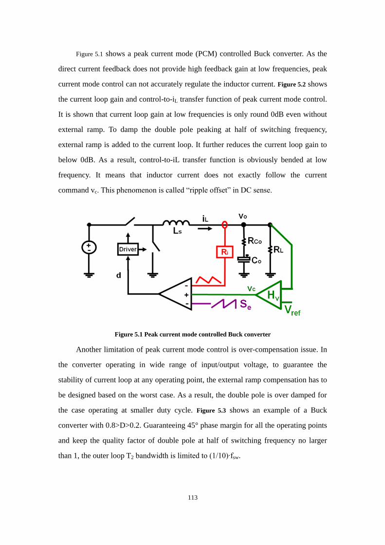
113
Figure 5.1 shows a peak current mode (PCM) controlled Buck converter. As the
direct current feedback does not provide high feedback gain at low frequencies, peak
current mode control can not accurately regulate the inductor current. Figure 5.2 shows
the current loop gain and control-to-iL transfer function of peak current mode control.
It is shown that current loop gain at low frequencies is only round 0dB even without
external ramp. To damp the double pole peaking at half of switching frequency,
external ramp is added to the current loop. It further reduces the current loop gain to
below 0dB. As a result, control-to-iL transfer function is obviously bended at low
frequency. It means that inductor current does not exactly follow the current
command vc. This phenomenon is called “ripple offset” in DC sense.
Figure 5.1 Peak current mode controlled Buck converter
Another limitation of peak current mode control is over-compensation issue. In
the converter operating in wide range of input/output voltage, to guarantee the
stability of current loop at any operating point, the external ramp compensation has to
be designed based on the worst case. As a result, the double pole is over damped for
the case operating at smaller duty cycle. Figure 5.3 shows an example of a Buck
converter with 0.8>D>0.2. Guaranteeing 45° phase margin for all the operating points
and keep the quality factor of double pole at half of switching frequency no larger
than 1, the outer loop T2 bandwidth is limited to (1/10)∙fsw.

114
Figure 5.2 Peak current mode controlled Buck converter
Figure 5.3 Overcompensation limits the control bandwidth
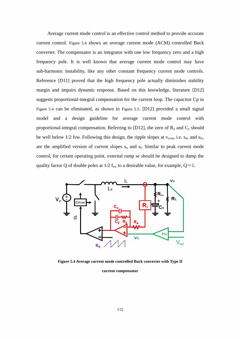
115
Average current mode control is an effective control method to provide accurate
current control. Figure 5.4 shows an average current mode (ACM) controlled Buck
converter. The compensator is an integrator with one low frequency zero and a high
frequency pole. It is well known that average current mode control may have
sub-harmonic instability, like any other constant frequency current mode controls.
Reference [D11] proved that the high frequency pole actually diminishes stability
margin and impairs dynamic response. Based on this knowledge, literature [D12]
suggests proportional-integral compensation for the current loop. The capacitor Cp in
Figure 5.4 can be eliminated, as shown in Figure 5.5. [D12] provided a small signal
model and a design guideline for average current mode control with
proportional-integral compensation. Referring to [D12], the zero of Rz and Cz should
be well below 1/2 fsw. Following this design, the ripple slopes at vcom, i.e. snc and sfc,
are the amplified version of current slopes sn and sf. Similar to peak current mode
control, for certain operating point, external ramp se should be designed to damp the
quality factor Q of double poles at 1/2 fsw to a desirable value, for example, Q≈1.
Figure 5.4 Average current mode controlled Buck converter with Type II
current compensator

116
Figure 5.5 ACM controlled Buck converter with proportional-integral current
compensator
However, it is difficult to get perfect design of se because the slopes snc and sfc
vary for several reasons. First, for most of the applications using ACM operate with
wide duty cycle range, e.g. battery charger and Power-Factor-Correction applications.
Different input and output voltage combinations vary the current slope in a wide
range. Second, the inductor and current sensing components have the tolerance
between 80%-150% due to the manufacture tolerance and temperature variation.
Third, the limited bandwidth of practical operation amplifier can cause slope
distortion at vcom. This distortion leads to a higher quality factor Q or even
sub-harmonic instability. Figure 5.6 shows the impact of the bandwidth of operation
amplifier on the control-to-iL transfer function. In the simulation, the switching
frequency is 300kHz. As the operating duty cycle is 0.13, if the current slope is
perfectly amplify by an ideal operation amplifier, the double pole at half of switching
frequency does not have peaking effect. However, the practical operation amplifiers
with 10MHz bandwidth distort the ripple slope and result in the peaking effect. If the
bandwidth is as low as 3.5MHz, the current loop becomes unstable. To stabilize the
current loop and suppress the peaking effect, certain external ramp Se has to be
applied to PWM comparator. As a result, control-to-iL transfer function exhibits much
more phase delay at frequencies above 1/10 of switching frequency.

117
In practice, the analog controller ICs are usually designed to compatible a wide
selection range of inductor and current sensing gain. Considering these limitations, for
simplicity of the controller, most of the commercial average current mode control ICs
apply a fixed large artificial ramp to guarantee the stability of the converter under all
the operating condition, different inductance and current sensing gain value. As a
penalty, the dynamic performance suffers from over compensation. Figure 5.7 shows
the current command step response of an average current mode controlled Buck
converter.
Figure 5.6 ACM controlled Buck converter with
proportional-integral current compensator

118
Figure 5.7 Current command step response of average current mode control
In order to improve the dynamic response, some literatures proposed various
method in [D13][D14][D15]. [D13] used hysteretic current mode control to achieve
average current control, by controlling both the peak current and valley current. As
the direct current feedback is never overwhelmed by external ramp, current control
bandwidth is high [D16][D17] and also enable a high bandwidth voltage loop.
However, hysteretic current mode control can only control average current in
continuous-conduction-mode (CCM), but does not work in
discontinuous-conduction-mode (DCM). Besides, the switching frequency in CCM of
this control is dependent on the actual value of the inductance. It brings difficulty in
filter design and synchronization. In order to make the switching frequency
independent on inductor, [D14] improved this control scheme by adding a frequency
regulation loop to change the width of hysteretic band, but average current is still not
controlled in DCM although it adds this complexity. [D15] modified conventional
average current mode control structure to get better transient response. The current
compensator is bypassed by a nonlinear loop during step transient of current
command. However, control circuit becomes more complicated, and the light load
efficiency issue is still unsolved due to the constant frequency operation.
5.3 Proposed I2 Average Current Mode Control
To improve the transient response and light load efficiency of ACM, I2 current
mode control is proposed in this paper. The general representation of I2 control is
illustrated in Figure 5.8. It consists of two current loops and a voltage loop. Inductor

119
current is fed back twice: one is a direct feedback without low pass filter and the other
is integral feedback. The integrator integrates the error between control signal vc and
inductor current iL and the output of the integrator is compared with the direct
feedback current signal to generate the PWM signal. Follow the terminology of “V2
control”, the proposed control scheme is named as “I2 control” [D18][D21]. In general,
this concept is applicable to constant frequency modulations and variable frequency
modulations.
Figure 5.8 Concept of proposed I2 average current mode control
As a particular embodiment of this concept, constant on-time I2 average current
mode control shows the additional advantage on light load efficiency improvement.
Small signal equivalent circuit model and design guideline are presented in section IV.
The proposed control scheme is verified by simulation and experimental results.
Figure 5.9 shows the proposed constant on-time I2 average current mode control
method. The current loop consists of a fast direct feedback loop and a slow integral
feedback loop. Voltage loop is the outer loop for voltage regulation.
In the particular embodiment using constant on-time modulation, at the
beginning of the switching cycle, the top switch turns on for a fix on-time. After the
on-time, the inductor current ramps down. The next cycle is triggered by the
intersection of inductor current and signal vci, which integrates the error between
average current command vc and sensed inductor current. The integration provides an

120
offset between vc and vci to eliminate low frequency control error. The integration
loop is low bandwidth so that the high frequency components are strongly attenuated.
During transient, the fast change of vc pass to vci as the Cin voltage does not have
abrupt change. The proposed control can achieve fast and accurate current control,
without external ramp required. In CCM, the switching frequency of I2 control is
independent on the inductor value. Figure 5.10 shows the simulation waveform of
current command vc step transient response in CCM.
Figure 5.9 Proposed Constant On-time I2 average current mode control
When average current is below half of the inductor current ripple, the circuit
operates in discontinuous-conduction-mode (DCM). In DCM, the synchronized
rectifier is turned off when inductor current reverses to minimize efficiency loss due
to reverse current flow and gate charge switching. At low load currents, vci will drop
below the zero current level. Both switches will remain off with the output capacitor
supplying the load current until the vci rises above the zero current level to initiate
another cycle. In this mode, frequency is proportional to load current at light loads.
Figure 5.11 shows the steady state waveforms of I2 current mode control in DCM.

121
Figure 5.10 Steady state operation and Transient Response of I2 control in CCM
Figure 5.11 Steady state operation of I2 control in DCM
5.4 Small Signal Model and Design Guideline
Inductor current direct feedback loop does not have a low pass filter, so all the
sideband frequency components (fsw-fm, fsw+fm, etc.) are fed back to the modulator.
The function of the integral current feedback is to eliminate the low frequency control
error, so it is a low bandwidth feedback. As a result, sideband frequency components
in this loop are so weak that they are negligible. Also, since the output voltage go

122
through the power stage low pass filter and compensator low pass filter, the outer loop
can be modeled by linear transfer function. Figure 5.12 shows the waveforms of the
current loop under sine perturbation. It is clear that only the inductor current
proportional feedback contains lots of high frequency component while vc and vci are
dominant by modulation frequency component. According to the analysis above, it is
reasonable to consider all the sideband frequency feedback effect in direct current
feedback loop, but only consider fundamental frequency in integral current feedback
and voltage loop. Figure 5.13 illustrates the frequency components of significance in
small signal modeling process.
Figure 5.12 The key waveforms in current loop under sine perturbation
Inductor current direct feedback loop is a highly nonlinear entity. Three-terminal
switch equivalent circuit model [D19] based on the result of describing function
derivation accurately predicts the small signal properties of this nonlinear entity up to
1/2 fsw. Substitute the closed current loop and the PWM switch by the by the
three-terminal equivalent circuit model, the equivalent circuit model of I2 control is
shown in Figure 5.14. The model is applicable to both variable frequency modulations
and constant frequency modulations. Solving the equivalent circuit, iL(s)/vci(s) is:
2
1
2
111
1
1
11
/)/()||()(
)(
sQssCRR
sCR
RR
R
Rsv
si
oLe
oL
Le
e
ici
L
where 2/
on
s
eT
LR ,
onT
1,
21Q
(5.1)

123
Figure 5.13 The frequency components of significance
Figure 5.14 Small signal equivalent circuit model
As shown in Figure 5.15, the high frequency vci to iL gain is determined by Ri. The
high frequency double pole is beyond 1/2 fsw , while the quality factor is always
positive. The direct feedback loop is inherently stable for all operating point, so no
ramp is needed.

124
There are a low frequency pole and a low frequency zero in transfer function
iL(s)/vci(s). The pole is always at a higher frequency than the zero. Beyond the pole,
the gain of iL(s)/vci(s) is purely determined by current sensing gain Ri. The position of
the pole is:
oLepCRR )||(
(5.2)
To eliminate the low frequency control error, the goal of current compensator is
to boost low frequency gain below. Design the cross over frequency of integration
loop between and well below 1/2 fsw, control-to-iL transfer function is (5.2). With both
current loop closed, inductor current is well control from DC to which is beyond 1/2
fsw.
2
1
2
111
11
/)/()(
)(
sQsRsv
si
ic
L
(5.3)
The current compensator only deals with the low frequency information so that
the Operation Amplifier does not need a high product gain-bandwidth. Figure 5.16
shows the comparison of control-to-iL transfer functions of I2 average current mode
control, implementing the current compensator by different operation amplifier. The
curve of ideal operation amplifier overlaps with the curve of a low-end 1MHz
gain-bandwidth operation amplifier. Because the current compensator only deals with
the low frequency integration, the proposed I2 control does not require high quality
operation amplifier with high gain-bandwidth product. The compensator can be
implemented by low-end operation amplifier to save the cost without performance
sacrifice.
5.5 Concept Extensions
The proposed concept can be extended to other modulations, including variable
frequency constant off-time I2 control, as well as constant frequency
trailing-edge-modulated peak current I2 control and leading-edge-modulated valley

125
current I2 control. Figure 5.17 shows the system diagram of trailing-edge-modulated
peak current I2 control.
Figure 5.15 The design of integral current loop Tii

126
Figure 5.16 The control to iL transfer functions using ideal amplifier and limited bandwidth amplifier
Figure 5.17 Constant frequency trailing-edge-modulated peak current I2 control

127
5.6 Simulation and Experimental Results
Figure 5.18 compares the proposed small signal model with SIMPLIS simulation
results. The model is accurate up to 1/2 switching frequency. In the simulations,
switching frequency fsw ≈ 300kHz, Vin=12V, Vo=1.2V, Ls=300nH, Co=4.48mF,
RL=0.1Ω and current sensing gain Ri=10mΩ.
Figure 5.18 Control-to-iL transfer function of I2 control in
continuous-conduction-mode
Experiment is done on a Buck converter prototype. In the experiment, switching
frequency fsw≈400kHz, Vin=12V, Vo=1.2V, Ls=2.2nH, Co=47μF, RL=0.3Ω and
current sensing gain Ri=0.28Ω. Figure 5.19 shows the waveforms of current controller
in steady state. Figure 5.20 shows the current command step transient response. It is
clear that current loop response is very fast. The average inductor current follows the
step change of current command vc in one switching cycle. Figure 5.21 and Figure 5.22
shows the comparison of control to inductor current transfer function and control to
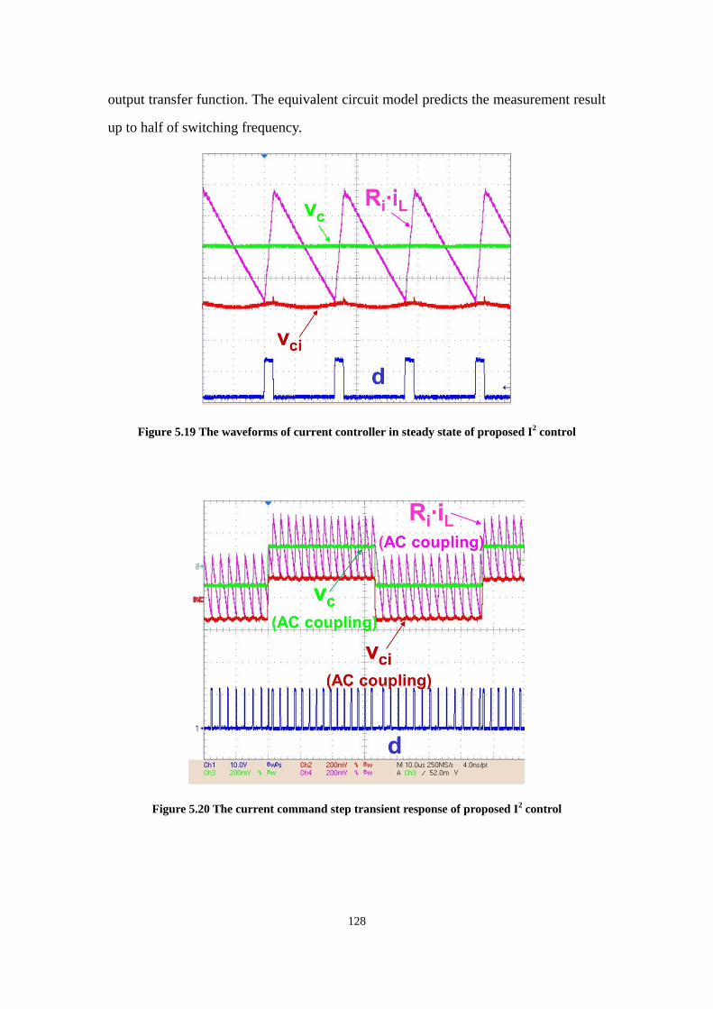
128
output transfer function. The equivalent circuit model predicts the measurement result
up to half of switching frequency.
Figure 5.19 The waveforms of current controller in steady state of proposed I2 control
Figure 5.20 The current command step transient response of proposed I2 control

129
Figure 5.21 Control-to-iL transfer function of I2 control
Figure 5.22 Control-to-vo transfer function of I2 control
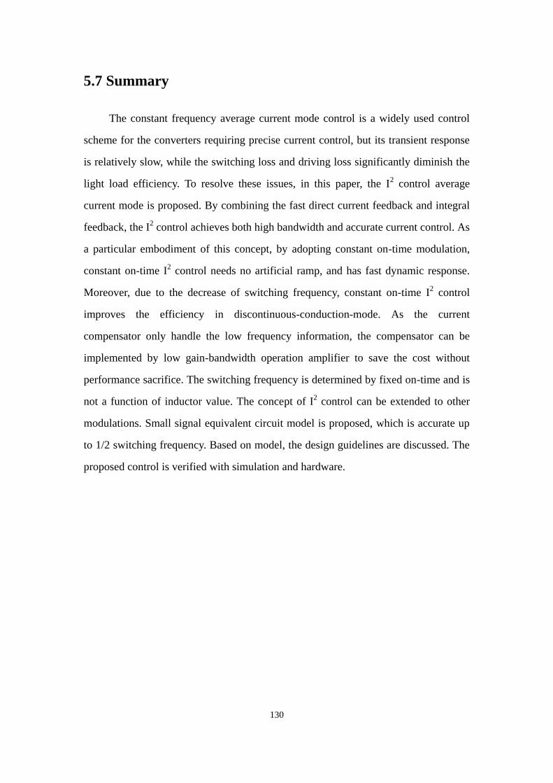
130
5.7 Summary
The constant frequency average current mode control is a widely used control
scheme for the converters requiring precise current control, but its transient response
is relatively slow, while the switching loss and driving loss significantly diminish the
light load efficiency. To resolve these issues, in this paper, the I2 control average
current mode is proposed. By combining the fast direct current feedback and integral
feedback, the I2 control achieves both high bandwidth and accurate current control. As
a particular embodiment of this concept, by adopting constant on-time modulation,
constant on-time I2 control needs no artificial ramp, and has fast dynamic response.
Moreover, due to the decrease of switching frequency, constant on-time I2 control
improves the efficiency in discontinuous-conduction-mode. As the current
compensator only handle the low frequency information, the compensator can be
implemented by low gain-bandwidth operation amplifier to save the cost without
performance sacrifice. The switching frequency is determined by fixed on-time and is
not a function of inductor value. The concept of I2 control can be extended to other
modulations. Small signal equivalent circuit model is proposed, which is accurate up
to 1/2 switching frequency. Based on model, the design guidelines are discussed. The
proposed control is verified with simulation and hardware.

131
Chapter 6. Conclusions and Future Work
6.1 Summary
Current-mode control architectures with different implementation approaches
have been widely used in many applications, such as voltage regulator, power factor
correction, battery charger and LED driver. An accurate model for current-mode
control is indispensable to system design. The early averaging models consider only
the fundamental frequency feedback and the sideband frequency feedback effect are
ignored. As a result, averaging models fail to predict the sub-harmonic instability of
current loop. Discrete time model and sample-data model capture the characteristic of
constant frequency current mode control and successfully predict the instability
problem, but the form of the models are inconvenient to use in engineering design.
Some modified averaging models borrow the result of sample-data model and are
widely used in industry. However, the fundamental assumption of sample-data
concept is invalid in variable frequency modulations, which are popular recently due
to the light load efficiency improvement. The continuous time model based on
describing function is one of the approaches which successfully model current mode
controls with constant frequency modulations and variable frequency modulations,
but the mathematical derivation is too complicated that the application in engineering
design is limited.
To make the accurate model of current mode control user friendly and universal,
a unified three-terminal switch model for current mode control is proposed. Based on
the observation, the PWM switch and the closed current loop is taken as an invariant
sub-circuit which is common to different PWM converter topologies. The Basic small
signal relationship is studied and the result shows that the PWM switch with current
feedback preserves the property of the PWM switch in power stage. A three-terminal
equivalent circuit is developed to represent the small signal behavior of this common

132
sub-circuit. The proposed model is a unified model, which is applicable in both
constant frequency modulation and variable frequency modulation. Proposed model is
extended to multiphase configurations. Based on the unified model, the merits and
limits of different implementations are compared.
Following the analysis of analog current mode control, the Laplace domain
small signal model for digital predictive current mode control is proposed. The
describing function method is applied to derive the small signal model. The model
covers peak current mode, valley current mode and average current mode control with
various modulations. The model is also extended to multi-sampling cases. Design
guidelines and comparison of modulation laws are discussed. The modeling results
are summarized as equivalent circuit model.
In Chapter 3, the small signal equivalent circuit model is extended to average
current mode control. It is shown that many existing models do not consider the ripple
of current compensator in a correct way. As a result, the accuracy of model at high
frequencies is unsatisfactory. By separating the feedback information of average
current mode control, the equivalent circuit model for average current mode control
using the proposed equivalent circuit is presented. The model includes the sideband
frequency feedback effect so that it is accurate up to half of switching frequency. The
design guidelines are investigated.
In Chapter 4, the small signal equivalent circuit model is extended to V2 current
mode control and enhanced V2 control. V
2 control is decomposed as current mode
control with proportional capacitor voltage feedback and load current feedback. The
load current feedback effectively reduces the output impedance. For Voltage
Regulator applications, the enhanced V2 control is a variety of V
2 control with
additional inductor current feedback to the output voltage. The enhanced V2 control is
analyzed using the equivalent circuit model in this chapter.
In Chapter 5, I2 average current mode control is proposed. I
2 current mode
control has two inductor current feedbacks: one is the direct feedback without low
133
pass filter, and the other one is the integral feedback. The small signal analysis based
on the proposed equivalent circuit model is presented. The concept of I2 control is
applicable to both constant frequency and variable frequency modulations. As a
particular embodiment, constant on-time I2 control is proposed to improve both
transient response and light load efficiency of average current mode control.
6.2 Future Work
In this dissertation, a three-terminal switch model is proposed to characterize the
small signal model of current mode control converters, including peak current mode
control, valley current mode control, charge control and constant on-time control and
constant off-time control. It is interesting to extend this concept to hysteresis current
mode control, which is a simple, popular current mode control scheme.
Furthermore, the equivalent circuit model for V2 control presented in Chapter 4 is
under the assumption that the output capacitor is ESR dominant. Further research may
be done to extend the application of the equivalent circuit model to the case that
capacitance is dominant, such as ceramic capacitor.

134
Reference
Part A
[A1] L. E. Galllaher, “Current Regulator with AC and DC Feedback,” U.S. Patent
3,350,628, 1967.
[A2] F. C. Schwarz, “Analog Signal to Discrete Time Interval Converter (ASDTIC),”
U. S. Patent 3,659,184, 1972.
[A3] A. Capel, G. Ferrante, D. O’Sullivan, and A. Weinberg, “Application of the
Injected Current Model for the Dynamic Analysis of Switching Regulators with
the New Concept of LC3 Modulator,” in proc. IEEE PESC’78, pp. 135-147.
[A4] A. D. Schoenfeld, Y. Yu, “ASDTIC Control and Standardized Interface Circuits
Applied to Buck, Parallel and Buck-Boost DC-to-DC Power Converters,” NASA
Report NASA CR-121106, February, 1973.
[A5] C. W. Deisch, “Switching Control Method Changes Power Converter into a
Current Source,” in proc. IEEE PESC’78, pp. 300-306.
[A6] R. Redl and N. O. Sokal, “Current-mode control, five different types, used with
the three basic classes of power converters: small-signal ac and large-signal dc
characterization, stability requirements, and implementation of practical circuits,”
in Proc. IEEE PESC’85, pp. 771-785.
[A7] W.Tang, Y.Jiang, G.C.Hua, F.C.Lee, I.Cohen, “Power Factor Correction With
Flyback Converter Employing Charge Control” in Proc. IEEE APEC’93, pp. 293
– 298, 1993.
[A8] P. L. Hunter, “Converter Circuit and Method Having Fast Responding Current
Balance and Limiting,” U.S. Patent 4,002,963, 1977.
[A9] L.H. Dixon, “Average Current-Mode Control of Switching Power Supplies,”
Unitrode Power Supply Design Seminar handbook, 1990, pp. 5.1-5.14
[A10] I. Cohen, “Adaptive control method for power converters,” U. S. Patent
5,438,505, 1995.
[A11] J. P. Bryant, “AC-DC power supply growth variation in China and North
America,” in proc. IEEE APEC’05, pp.159-162.
[A12] S. Varma, “Future power solutions,” Special Session Presentation of IEEE
APEC, 2005.
[A13] E. Stanford, “Power delivery challenges in computer platforms,” Special Session
Presentation of IEEE APEC, 2006.
[A14] B. Mammano, “Distributed power system,” Unitrode Seminar, SEM-900, 1993.
[A15] F. C. Lee, P. Barbosa, P. Xu, J. Zhang, B. Yang, and F. Canales, “Topologies and
design considerations for distributed power system applications,” in proc. IEEE,
vol. 89, no. 6, Jun. 2001, pp. 939–950.
[A16] P. Xu, W. Chen, J. Shao, P.-L. Wong, B. Yang, and F. C. Lee, “Development of 1

135
kW front-end module for DPS testbed,” in proc.CPES Annual Seminar, 2000, pp.
116-119.
[A17] B. Yang, “Topology Investigation for Front End DC/DC Power Conversion for
Distributed Power System”, Ph. D Dissertation, Virginia Tech, Blacksburg, 2003.
[A18] B. Lu, “Investigation of High-density Integrated Solution for AC/DC Conversion
of a Distributed Power System”, Ph. D Dissertation, Virginia Tech, Blacksburg,
2006.
[A19] J. Sun, “Dynamic Performance Analyses of Current Sharing Control for
DC/DC Converters,” Ph. D. dissertation, Virginia Tech., 2007
[A20] Intel document, “Voltage Regulator-Down (VRD) 11.0 Processor Power Delivery
Design Guidelines for Desktop LGA775 Socket,” November, 2006, Available at
http://www.intel.com.
[A21] R. Redl, B. P. Erisman and Z. Zansky, “Optimizing the Load Transient Response
of the Buck Converter,”in proc. IEEE APEC’98, pp. 170-176.
[A22] K. Yao, Y. Meng, P. Xu and F. C. Lee, “Design Considerations for VRM
Transient Response Based on the Output Impedance,” in proc. IEEE APEC’02,
pp. 14-20.
[A23] K. Yao, M. Xu, Y. Meng, and F. C. Lee, “Design considerations for VRM
transient response based on theoutput impedance,” IEEE Trans. Power Electron.,
Vol. 19, Issue 6, Nov. 2004, pp. 1454-1461.
[A24] K. Yao, K. Lee, M. Xu, and F. C. Lee, “Optimal design of the active droop
control method for the transient response,” in proc. IEEE APEC’03, pp. 718-723.
[A25] K. Yao, Y. Ren, J. Sun, K. Lee, M. Xu, J.i Zhou and F. C. Lee, “Adaptive
Voltage Position Design for Voltage Regulators,” in proc. IEEE APEC’04, pp.
272-278.
[A26] “NCP5331: Two Phase CPU Controller with Integrated Gate Drivers for AMD's
Athlon Processor,” ON Semiconductor document.
[A27] Chen Zhou, etc, “Design trade-offs in continuous current-mode controlled boost
power-factor correction circuits”, in Proceeding of HFPC’92, 1992.
[A28] “CS5151CPU 4−Bit Nonsynchronous Buck Controller,” ON Semiconductor
document.
[A29] “3-Phase+1-Phase, D-CAP+ step down controller for IMVP7 CPU/GPU Vcore,
TPS51640 datasheet,” Texas Instruments document.
[A30] “3-Phase+1-Phase, Quick-PWM Controller for VR12/IMVP7, MAX17039
datasheet,” Maxim document.
[A31] J.P.Gegner, C.Q.Lee, “Linear peak current mode control a: simple active power
factor correction co ntrol,” in proc. IEEE PESC '96, pp. 196 - 202.
[A32] C. Adragna, “AN1792 Design of fixed-off-time- controlled pfc pre-regulators
with the l6562,” ST Semiconductor Application Note, 2003.
[A33] C.Adragna, S.De Simone, G.Gattavari, “New Fixed Off-Time PWM Modulator
Provides Constant Frequency Operation in Boost PFC Pre-regulators,” in proc.
SPEEDAM’08, pp. 656 - 661.
[A34] Maxim, MAX8713 datasheet,
http://datasheets.maxim-ic.com/en/ds/MAX8713.pdf
136
[A35] Linear Technology, LTC1980 datasheet,
http://cds.linear.com/docs/Datasheet/1980f.pdf
[A36] E.F. Schubert, “Light-emitting diodes(Second Edition)”, Cambridge University
Press, 2006.
[A37] LUMILEDS, "Luxeon III Emitter Technical Datasheet DS45",
http://www.sparkfun.com/datasheets/Components/Luxeon-III.pdf
[A38] ON Semiconductor, NCL30100 datasheet,
http://www.onsemi.cn/pub_link/Collateral/NCL30100-D.PDF
[A39] Linear Technology, LTC3452 datasheet,
http://cds.linear.com/docs/Datasheet/3452f.pdf
[A40] Intersil, ISL97632 datasheet, http://www.intersil.com/data/fn/fn9239.pdf
[A41] S. P. Hsu, A. Brown, L. Rensink, and R. D. Middlebrook, “Modeling and
analysis of switching dc-to-dc converters in constant-frequency
current-programmed mode,” in proc. IEEE PESC’79, pp. 284-301.
[A42] G. W. Wester and R. D. Middlebrook, “Low Frequency characterization of
switched dc-to-dc converters,” in proc. IEEE PESC’72, pp. 9-20.
[A43] R.D. Middlebrook and S. Cuk, “A General Unified Approach to Modeling
Switching-Converter Power Stages” in proc. IEEE PESC’76, pp. 18-34.
[A44] R. Dirkman, “Generalized State Space Averaging”, in proc. IEEE PESC’83, pp.
283-294.
[A45] F.C. Lee and D.J. Shortt, "An Improved Switching Converter Power Model Using
Discrete and Average Techniques," in proc. IEEE PESC’82, pp.199-212.
[A46] S. Cuk and R. D. Middlebrook, “A General Unified Approach to Modeling
Switching Dc-to-Dc Converters in Discontinuous Conduction Mode,” in proc.
IEEE PESC’77, pp. 36-57.
[A47] V. Vorperian, “Simplified analysis of PWM converters using model of PWM
switch. Continuous conduction mode,” IEEE Trans. Aerosp., Vol. 26, pp. 490
–496, May 1990.
[A48] V. Vorperian, “Simplified analysis of PWM converters using model of PWM
switch. II. Discontinuous conduction mode,” IEEE Trans. Aerosp., Vol. 26, pp.
497 -505, May 1990.
[A49] F.C. Lee, Y. Yu, and M.F. Mahmoud, “A Unified Analysis and Design Procedure
for a Standardized Control Module for DC-DC Switching Regulators, ” in proc.
IEEE PESC’80, pp.284-301.
[A50] R. D. Middlebrook, “Topics in Multiple-Loop Regulators and Current Mode
Programming,” in proc. IEEE PESC’85, pp. 716-732.
[A51] R.D. Middlebrook, “Modeling Current-Programmed Buck and Boost
Regulators,” IEEE Trans. Power Electron., Vol. 4, pp. 36-52, January 1989.
[A52] R. Martinelli, “The Benefits of Multi-Loop Feedback,” in proc. PCI’87, pp.
227-245.
[A53] G.K. Schoneman and D. M. Mitchell, “Output Impedance Considerations for
Switching Regulators with Current-Injected Control,” IEEE Trans. Power
Electron., vol. 4, pp. 25-35, January 1989.
[A54] V. G. Bello, “Using the SPICE2 CAD Package to Simulate an Design the

137
Current-Mode Converter,” in proc. POWERCON’84, paper H-2.
[A55] B. Holland, “Modelling, Analysis and Compensation of the Current-Mode
Converter,” in proc. POWERCON’84, paper H-2.
[A56] A. S. Kislovski, “Controlled-Quantity Concept in Small-Signal Analysis of
Switching Power Cells,” IEEE Trans. Aerosp., Vol. AES-19, No. 3, pp.
438-446,1983.
[A57] L. H. Dixon, “Closing the Feedback Loop”, Appendix C, Unitrode Power Design
Seminar, pp. 2C1-2C18, 1983.
[A58] A. S. Kislovski, “Current-Mode Control: a Unified Model for Open-loop
Stability,” in proc. IEEE APEC’91, pp. 459-465.
[A59] V. Voqkrian, “Analysis of current-mode controlled PWM converters using the
model of the current-controlled PWM switch,” in proc. PCIM Con’90.
[A60] D. J. Packard, “Discrete Modeling and Analysis of Switching Regulators,” Ph.D.
dissertation, Cal. Tech., CA, May 1976
[A61] A. R. Brown and R. D. Middlebrook, “Sample-Data Modeling of Switched
Regulators,” in proc. IEEE PESC’81, pp. 349-369.
[A62] G. C. Verghese, C. A. Bruzos, and K. N. Mahabir, “Averaged and sample-data
models for current mode control: A reexamination,” in Proc. IEEE PESC’89, pp.
484-491.
[A63] R. Redl, “High-frequency extension of the small-signal model of the
constant-frequency current-mode-controlled converter,” in proc. IEEE APEC '91,
pp. 466 – 472.
[A64] R. B. Ridley, “A new, continuous-time model for current-mode control,” IEEE
Trans. Power Electron., vol. 6, no. 2, pp. 271-280, April 1991.
[A65] R. Tymerski and D. Li, “State-space models for current-programmed
pulsewidth-modulated converters,” IEEE Trans. Power Electron., vol.8, no. 3, pp.
271-278, July 1993.
[A66] F. D. Tan and R. D. Middlebrook, “A unfied model for current-programmed
converters,” IEEE Trans. Power Electron., vol. 10, no. 4, pp.397–408, Jul. 1995.
[A67] D. J. Perreault and G. C. Verghese, “Time-varying effects for current-mode
control,” in proc. IEEE PESC’95, pp. 621-628.
[A68] M. K. Kazimierczuk, “Transfer function of current modulator in pwm converters
with current-mode control,” IEEE Trans. Circuits and Systems I, vol. 47, no. 9,
pp. 1407-1412, Sep. 2000.
[A69] E. A. Mayer and A. J. King, “An improved sampled-data current-mode control
which explains the effects of the control delay,” IEEE Trans. Power Electron.,
vol. 16, no. 3, pp. 369-374, May. 2001.
[A70] B. Bryant and M. K. Kazimierczuk, “Modeling the closed-current loop of pwm
dc-dc converters operating in ccm with peak current-mode control,” IEEE Trans.
Circuits and Systems, vol. 52, no. 11, pp. 2404-2412, Nov. 2005.
[A71] W. Tang, F. C. Lee, and R. B. Ridley, “Small-signal modeling of average
current-mode control,” IEEE Trans. Power Electron., vol. 8, pp. 112-119, April
1993.
[A72] W. Tang, F. C. Lee, R. B. Ridley, and I. Cohen, “Charge control: modeling,
138
analysis, and design,” IEEE Trans. Power Electron., vol. 8, pp. 396-403, Oct.
1993.
[A73] Y.-W. Lo and R. J. King, “Sampled-data modeling of the average-input
current-mode-controlled buck converter”, IEEE Trans. Power Electron., vol. 14,
no. 5, pp. 918-927, Sept. 1999.
[A74] R. B. Ridley, “A new continuous-time model for current-mode control with
constant frequency, constant on-time, and constant off-time, in CCM and DCM,”
in proc. IEEE PESC’90, pp. 382- 389.
[A75] J. Li, “Current-Mode Control: Modeling and its Digital Application,” Ph. D.
Dissertation, Virginia Tech, 2009.
[A76] A. Gelb, and W. E. Vander Velde: Multiple-Input Describing Functions and
Nonlinear System Design, McGraw Hill, 1968.
[A77] Xiaoru Xu, Xiaobo Wu, Xiaolang Yan, “A Quasi Fixed Frequency Constant On
Time Controlled Boost Converter,” in proc. IEEE ISCAS’08, pp. 2206 – 2209,
2008.
[A78] J.T.Mossoba, P.T.Krein, “Output Impedance of High Performance Current Mode
dc-dc Buck Converters, with Applications to Voltage-Regulator Module Control
Combinations,” in proc. IEEE APEC '04, pp. 1315 - 1321.
[A79] N.Kondrath, M.K.Kazimierczuk, “Control-to-Output and Duty Ratio-to-Inductor
Current Transfer Functions of Peak Current-Mode Controlled DC-DC PWM
Buck Converter in CCM,” in proc. IEEE ISCAS '10, pp. 2734 - 2737.
[A80] C. Wang, “Investigation on Interleaved Boost Converters and Applications,” Ph.
D. Dissertation, Virginia Tech, 2009.
[A81] R. Redl, “Small-signal high-frequency analysis of the free-running
current-mode-controlled converter,” in proc. IEEE PESC '91, pp. 897 – 906.
[A82] R. D. Middlebrook, “Predicting modulator phase lag in PWM converter feedback
loops,” In proc. POWERCON’ 81, paper H-4.
Part B
[B1] O'Sullivan, D.; Spruyt, H.; Crausaz, A.; , "PWM conductance control," Power
Electronics Specialists Conference, 1988. PESC '88 Record., 19th Annual IEEE ,
vol., no., pp.351-359 vol.1, 11-14 April 1988
[B2] Y. Qiu, M. Xu, K. Yao, J. Sun, and F. C. Lee, “Multifrequency small signal
model for buck and multiphase buck converters,” IEEE Trans. Power Electron.,
vol. 21, no. 5, pp. 1185–1192, Sep. 2006.
[B3] Jian Li; Lee, F.C.; , "New Modeling Approach and Equivalent Circuit
Representation for Current-Mode Control," Power Electronics, IEEE
Transactions on , vol.25, no.5, pp.1218-1230, May 2010
[B4] L. H. Dixon, “Average Current Mode Control of Switching Power Supplies,”
Unitrode Power Supply Design Seminar Manual, 1990.
[B5] Kislovski, A.S.; , "Small-signal, low-frequency analysis of a buck type PWM
conductance controller," Power Electronics Specialists Conference, 1990. PESC

139
'90 Record., 21st Annual IEEE , vol., no., pp.88-95, 11-14 Jun 1990
[B6] Ruqi Li; , "Modeling Average-Current-Mode-Controlled multi-phase buck
converters," Power Electronics Specialists Conference, 2008. PESC 2008. IEEE ,
vol., no., pp.3299-3305, 15-19 June 2008
[B7] Sun, J.; Bass, R.M.; , "Modeling and practical design issues for average current
control ," Applied Power Electronics Conference and Exposition, 1999. APEC
'99. Fourteenth Annual , vol.2, no., pp.980-986 vol.2, 14-18 Mar 1999
[B8] Ruqi Li; O'Brien, T.; Lee, J.; Beecroft, J.; , "A unified small signal analysis of
DC-DC converters with Average Current Mode Control," Energy Conversion
Congress and Exposition, 2009. ECCE 2009. IEEE , vol., no., pp.647-654, 20-24
Sept. 2009
[B9] Cooke, P.; , "Modeling average current mode control," Applied Power
Electronics Conference and Exposition, 2000. APEC 2000. Fifteenth Annual
IEEE , vol.1, no., pp.256-262 vol.1, 2000
[B10] Suntio, T.; Lempinen, J.; Gadoura, I.; Zenger, K.; , "Dynamic effects of inductor
current ripple in average current mode control," Power Electronics Specialists
Conference, 2001. PESC. 2001 IEEE 32nd Annual , vol.3, no., pp.1259-1264 vol.
3, 2001
[B11] A. R. Brown and R. D. Middlebrook, “Sample-data modeling of switched
regulators,” in Proc. IEEE PESC 1981, pp. 349–369.
[B12] R. B. Ridley, “A new, continuous-time model for current-mode control,” IEEE
Trans. Power Electron., vol. 6, no. 2, pp. 271–280, Apr. 1991.
[B13] Tang, W.; Lee, F.C.; Ridley, R.B.; , "Small-signal modeling of average
current-mode control," Power Electronics, IEEE Transactions on , vol.8, no.2,
pp.112-119, Apr 1993
[B14] Young-Seek Jung; Myung-Joong Youn; , "Discrete time small signal modeling of
average current mode control," Electronics Letters , vol.36, no.23, pp.1908-1909,
9 Nov 2000
[B15] Jung, Y.-S.; Youn, M.-J.; , "Sampling effect in continuous-time small-signal
modelling of average-current mode control," Electric Power Applications, IEE
Proceedings - , vol.149, no.4, pp. 311- 316, July 2002
[B16] Chunxiao Sun; Lehman, B.; , "Discussions on control loop design in average
current mode control," Industry Applications Conference, 2000. Conference
Record of the 2000 IEEE , vol.4, no., pp.2411-2417 vol.4, Oct 2000
[B17] Feng Yu; Lee, F.C.; Mattavelli, P.; , "A small signal model for average current
mode control based on describing function approach," Energy Conversion
Congress and Exposition (ECCE), 2011 IEEE , vol., no., pp.405-412, 17-22 Sept.
2011
[B18] Yingyi Yan; Lee, F.C.; , "Unified three-terminal switch model for current mode
controls," Energy Conversion Congress and Exposition (ECCE), 2010 IEEE ,
vol., no., pp.1965-1972, 12-16 Sept. 2010
[B19] Yan, Y.; Lee, F. C.; Mattavelli, P.; , "Unified Three-Terminal Switch Model for
Current Mode Controls," Power Electronics, IEEE Transactions on , vol.27, no.9,
pp.4060-4070, Sept. 2012

140
Part C
[C1] D. Goder and W. R. Pelletier, “V2 architecture provides ultra-fast transient
response in switch mode power supplies," in proc. HFPC’96, pp. 19-23.
[C2] J. Sun, “Characterization and performance comparison of ripple-based control for
voltage regulator modules,” IEEE Trans. Power Electron.,vol.21, pp. 346 – 353,
March 2006.
[C3] W. Huang and J. Clarkin, “Analysis and design of multiphase synchronous buck
converter with enhanced V2 control,” in Proc.HFPC’00, 2000, pp. 74–81.
[C4] “3-Phase+1-Phase, D-CAP+ step down controller for IMVP7 CPU/GPU Vcore,
TPS51640 datasheet,” Texas Instruments document.
[C5] “3-Phase+1-Phase, Quick-PWM Controller for VR12/IMVP7, MAX17039
datasheet,” Maxim document.
[C6] Huang, W.; , "A new control for multi-phase buck converter with fast transient
response," Applied Power Electronics Conference and Exposition, 2001. APEC
2001. Sixteenth Annual IEEE , vol.1, no., pp.273-279 vol.1, 2001
[C7] S. Qu, “Modeling and design considerations of V2 controlled buck regulator,” in
Proc. IEEE APEC’01, Anaheim, California, pp. 507–513.
[C8] Jian Li; Lee, F.C.; , "New Modeling Approach and Equivalent Circuit
Representation for Current-Mode Control," Power Electronics, IEEE
Transactions on , vol.25, no.5, pp.1218-1230, May 2010
[C9] Jian Li; Lee, F.C.; , "Modeling of V2 Current-Mode Control," Circuits and
Systems I: Regular Papers, IEEE Transactions on , vol.57, no.9, pp.2552-2563,
Sept. 2010.
[C10] Feng Yu; Lee, F.C.; , "Design oriented model for constant on-time V2 control,"
Energy Conversion Congress and Exposition (ECCE), 2010 IEEE , vol., no.,
pp.3115-3122, 12-16 Sept. 2010
[C11] Yan, Y.; Lee, F. C.; Mattavelli, P.; , "Unified Three-Terminal Switch Model for
Current Mode Controls," Power Electronics, IEEE Transactions on , vol.27, no.9,
pp.4060-4070, Sept. 2012
[C12] Yingyi Yan; Lee, F.C.; , "Unified three-terminal switch model for current mode
controls," Energy Conversion Congress and Exposition (ECCE), 2010 IEEE ,
vol., no., pp.1965-1972, 12-16 Sept. 2010
[C13] Lin, Y.; Chen, C.; Chen, D.; Wang, B.; , "A Ripple-Based Constant On-Time
Control with Virtual Inductor Current and Offset Cancellation for DC Power
Converters," Power Electronics, IEEE Transactions on , vol.PP, no.99, pp.1, 0
[C14] Feng Su; Wing-Hung Ki; , "Digitally assisted quasi-V2 hysteretic buck converter
with fixed frequency and without using large-ESR capacitor," Solid-State Circuits
Conference - Digest of Technical Papers, 2009. ISSCC 2009. IEEE International ,
vol., no., pp.446-447,447a, 8-12 Feb. 2009
[C15] del Viejo, M.; Alou, P.; Oliver, J.A.; Garcia, O.; Cobos, J.A.; , "V2IC control: A
novel control technique with very fast response under load and voltage steps,"
141
Applied Power Electronics Conference and Exposition (APEC), 2011
Twenty-Sixth Annual IEEE , vol., no., pp.231-237, 6-11
[C16] Yuan Yen Mai; Mok, P.; , "A Constant Frequency Output-Ripple-Voltage-Based
Buck Converter Without Using Large ESR Capacitor,"Circuits and Systems II:
Express Briefs, IEEE Transactions on, vol.55, no.8, pp.748-752, Aug. 2008
[C17] “Fixed Frequency, 99% Duty Cycle Peak Current Mode Notebook System Power
Controller, TPS54220 datasheet,” Texas Instruments document.
[C18] “NCP5422A: Dual Out-of-Phase Synchronous Buck Controller”, ONSEMI
document.
[C19] G. Schuellein, “Current Sharing of Redundant Synchronous Buck Regulators
Powering High Performance Microprocessors using the V2 Control Method,”
Proceedings of APEC, 1998
[C20] Yang Qiu; Ming Xu; Kaiwei Yao; Sun, J.; Lee, F.C.; , "Multifrequency
Small-Signal Model for Buck and Multiphase Buck Converters," Power
Electronics, IEEE Transactions on, vol.21, no.5, pp.1185-1192, Sept. 2006
[C21] Yingyi Yan; Lee, F.C.; Mattavelli, P.; , "Dynamic performance comparison of
current mode control schemes for Point-of-Load Buck converter application,"
Applied Power Electronics Conference and Exposition (APEC), 2012
Twenty-Seventh Annual IEEE , vol., no., pp.2484-2491, 5-9 Feb. 2012
[C22] Yingyi Yan; Lee, F.C.; Mattavelli, P.; , " Comparison of Small Signal
Characteristics in Current Mode Control Schemes for Point-of-Load Buck
Converter Applications," IEEE Transactions on Power Electronics, 2013
[C23] Kuang-Yao Cheng; Feng Yu; Yingyi Yan; Lee, F.C.; Mattavelli, P.; Wenkai Wu;
, "Analysis of multi-phase hybrid ripple-based adaptive on-time control for
voltage regulator modules," Applied Power Electronics Conference and
Exposition (APEC), 2012 Twenty-Seventh Annual IEEE , vol., no.,
pp.1088-1095, 5-9 Feb. 2012
Part D
[D1] Lee, F.C. , Carter, R.A., Fang, Z.D, “Investigations of stability & dynamic
performances of a current-injected regulator”, IEEE Transactions on Aerospace
and Electronic Systems, March 1983.
[D2] C. W. Deisch, “Switching control method changes power converter into a current
source,” in proc. IEEE PESC’78, pp. 300-306.
[D3] “Hot-Swap N+1 Redundant XPhase Control IC, IR3510 datasheet,” International
Rectifier document, http://www.irf.com/indexnsw.html.
[D4] “VRM 9.0/VRM 9.1, Dual-Phase, Parallelable, Average-Current-Mode
Controller,” Maxim Integrated document, http://www.maxim-ic.com/.
[D5] “0.6V to 5.5V Output, Parallelable, Average-Current-Mode DC-DC Controllers,
MAX5060 datasheet,” Maxim Integrated document, http://www.maxim-ic.com/.

142
[D6] “Average Current Mode PWM Controller IC, UC3886 datasheet,” Texas
Instruments document, http://www.ti.com/.
[D7] “High Current Synchronous Step-Down LED Driver with Three-State Control,
LT3743 datasheet,” Linear Technology document, http://www.linear.com/.
[D8] “Switch-mode Lead-Acid Battery Charger with Differential Current Sense,
UC3909 datasheet,” Texas Instruments document, http://www.ti.com/.
[D9] “Fixed Frequency Average Current Mode Power Factor Corrector, L4981
datasheet,” ST Microelectronics document, http://www.st.com.
[D10] “Automotive Average Current Mode Controller, NCV8851B datasheet,” ON
Semiconductor document, http:// www.onsemi.com.
[D11] Feng Yu; Lee, F.C.; Mattavelli, P.; , "A small signal model for average current
mode control based on describing function approach," Energy Conversion
Congress and Exposition (ECCE), 2011 IEEE , vol., no., pp.405-412, 17-22 Sept.
2011
[D12] Yan, Y.; Lee, F. C.; Mattavelli, P.; , "Analysis and Design of Average Current
Mode Control Using Describing Function-Based Equivalent Circuit Model,”
Energy Conversion Congress and Exposition (ECCE), 2012 IEEE, vol., no.,
pp.2237-2244, 15-20 Sept. 2012
[D13] M.McJimsey, “Switching regulator with average current mode control”, US
Patent: US 7,170,267 B1, 2007
[D14] E.Coleman, “Frequency regulated hysteretic average current mode converter”,
US Patent: US 8,054,056 B2, 2011
[D15] J.Caldwell, “Average Inductor Current Mode Switching Converters”, US Patent:
US 8,120,335 B2, 2012
[D16] Park, J.H.; Ch, B.H.; , "Small signal modeling of hysteretic current mode control
using the PWM switch model," Computers in Power Electronics, 2006. COMPEL
'06. IEEE Workshops on, pp.225-230, 16-19 July 2006
[D17] Wang Jianhua; Liu Lei; Zhang Fanghua; Gong Chunying; Ma Yiling; ,
"Modeling and Analysis of Hysteretic Current Mode Control Inverter," Applied
Power Electronics Conference and Exposition, 2009. APEC 2009. Twenty-Fourth
Annual IEEE, pp.1338-1343, 15-19 Feb. 2009
[D18] D. Goder and W. R. Pelletier, “V2 architecture provides ultra-fast transient
response in switch mode power supplies," in proc. HFPC’96, pp. 19-23.
[D19] Yingyi Yan; Lee, F.C.; , "Unified three-terminal switch model for current mode
controls," Energy Conversion Congress and Exposition (ECCE), 2010 IEEE ,
vol., no., pp.1965-1972, 12-16 Sept. 2010
[D20] Yan, Y.; Lee, F. C.; Mattavelli, P.; , "Unified Three-Terminal Switch Model for
Current Mode Controls," IEEE Transactions on Power Electronics, , vol.27, no.9,
pp.4060-4070, Sept. 2012
[D21] Yingyi Yan; Lee, F.C.; Mattavelli, P.; , " Small Signal Analysis of V2 Control
Using Current Mode Equivalent Circuit Model," Applied Power Electronics
Conference and Exposition (APEC), 2013 Twenty-Eighth Annual IEEE , 17-21
March. 2013

143
[D22] Yingyi Yan; Lee, F.C.; Mattavelli, P.; , "Dynamic performance comparison of
current mode control schemes for Point-of-Load Buck converter application,"
Applied Power Electronics Conference and Exposition (APEC), 2012
Twenty-Seventh Annual IEEE , vol., no., pp.2484-2491, 5-9 Feb. 2012
[D23] Yingyi Yan; Lee, F.C.; Mattavelli, P.; , " Comparison of Small Signal
Characteristics in Current Mode Control Schemes for Point-of-Load Buck
Converter Applications," IEEE Transactions on Power Electronics, 2013
Part E
[E1] Lee, F.C. , Carter, R.A., Fang,Z.D, “Investigations of Stability & Dynamic
Performances of a Current-Injected Regulator”, IEEE Transactions on Aerospace
and Electronic Systems, March 1983.
[E2] J. Li, F.C. Lee, “New Modeling Approach and Equivalent Circuit Representation
for Current-Mode Control,” IEEE Transactions on Power Electronics, vol. 25,
no. 5, pp. 1218 - 1230, May 2010
[E3] R. D. Middle Brook, “Topics in multiple-loop regulators and current mode
programming,” in Proc. IEEE PESC 1985, pp. 716–732.
[E4] R. B. Ridley, “ A new, continuous-time model for current-mode control,” IEEE
Transactions on Power Electronics, vol. 6, no. 2, pp. 271-280, April 1991
[E5] Shirazi, M. ; Zane, R. ; Maksimovic, D. ; Corradini, L. , Mattavelli, P. ,
“Autotuning Techniques for Digitally-Controlled Point-of-Load Converters with
Wide Range of Capacitive Loads ”, in Proc. IEEE Applied Power Electronics
Conference, APEC 2007., pp:14-20.
[E6] Kuang-Yao Cheng; Feng Yu; Mattavelli, P.; Lee, F.C.; , "Digital enhanced
V2-type constant on-time control using inductor current ramp estimator for a
buck converter with small ESR capacitors," Energy Conversion Congress and
Exposition (ECCE), 2010 IEEE , vol., no., pp.508-513, 12-16 Sept. 2010
[E7] Mattavelli, P. Polo, F. Dal Lago, F. Saggini, S., “Analysis of Control-Delay
Reduction for the Improvement of UPS Voltage-Loop Bandwidth”, IEEE
Transactions on Industrial Electronics, Aug. 2008.
[E8] Voss, I., Schroder, S., De Doncker, R. W.,“Predictive Digital Current Control
Using Advanced Average Current Sampling Algorithm for Multi-Phase
2-Quadrant DC/DC Converters”, in Proc. IEEE Applied Power Electronics
Conference, APEC 2007., pp:8-13.
[E9] Jingquan Chen, Dragan Maksimovic, etc. ,“Predictive digital current programmed
control,” IEEE Transactions on Power Electronics, 2003.
[E10] S. Chattopadhyay, S. Das, “A digital current-mode control technique for dc-dc
converters,” IEEE Trans. Power Electronics, vol.21, no.6, pp.1718-1726, Nov.
2006.
[E11] Guohua Zhou, “Digital Peak Current Control for Switching DC–DC Converters
with Asymmetrical Dual-Edge Modulation,” IEEE Transactions on Circuits And
Systems, 2009.
[E12] Guohua Zhou, Jianping Xu, “Asymmetrical leading-triangle modulation
technique for improved digital valley current controlled switching DC-DC
144
converters”, in Proc. IEEE Energy Conversion Congress and Exposition
(ECCE)2010, pp:237-241.
[E13] Kai Wan, M. Ferdowsi, “Reducing computational time delay in digital
current-mode controllers for dc-dc converters”, in Proc. IEEE 30th International
Telecommunications Energy Conference, 2008.
[E14] Bibian, S.; Jin, H.; , "High performance predictive dead-beat digital controller for
DC power supplies," Applied Power Electronics Conference and Exposition,
2001. APEC 2001. Sixteenth Annual IEEE , vol.1, no., pp.67-73 vol.1, 2001
[E15] Yen-Shin Lai, Chia-An Yeh, “Predictive Digital-Controlled Converter With Peak
Current-Mode Control and Leading-Edge Modulation”, IEEE Transactions on
Industrial Electronics, June 2009.
[E16] Bolton, A.G., “Design of sampled control systems using Laplace domain
techniques”, IEE Proceedings of Electronic Circuits and Systems,
vol.128 , Issue:3 pp: 138-142. June 1981.
[E17] Hung-Shou Nien, Dan Chen, Wei-Hsu Chang, “Small-Signal Modeling of DC
Converters with Digital Peak-Current-Mode Control”, in Proc. IEEE Power
Electronics Specialists Conference, 2008, pp. 3266-3271.
[E18] C.-H. Chen, W.-H. Chang, D. Chen, L.-P. Tai, and C.-C. Wang, “Modeling of
Digitally Controlled Voltage-Mode DC-DC Converters,” in Proc. IEEE
Industrial Electronics conference, Nov 6-8, 2007.
[E19] Van de Sype, D.M. ; De Gusseme, K. ; Van den Bossche, A.P. ; Melkebeek,
J.A. ;, “Small-signal Laplace-domain analysis of uniformly-sampled pulse-width
modulators”, in Proc. IEEE Power Electronics Specialists Conference, 2004, pp.
4292-4298.
[E20] G. F. Franklin, J. D. Powell, and M. L. Workman, Digital Control of Dynamic
Systems, 3rd ed. Reading, MA: Addison Wesley, 1998.
[E21] Duan, Y.; Jin, H.; , "Digital controller design for switch mode power converters,"
Applied Power Electronics Conference and Exposition, 1999. APEC '99.
Fourteenth Annual , vol.2, no., pp.967-973 vol.2, 14-18 Mar 1999
[E22] L.Corradini, P.Mattavelli, “Modeling of Multisampled Pulse Width Modulators
for Digitally Controlled DC–DC Converters”, IEEE Transactions on Power
Electronics, July 2008.
[E23] Tang, W. ; Lee, F.C. ; Ridley, R.B., “Small-signal modeling of average
current-mode control”, in Proc. Applied Power Electronics Conference and
Exposition, 1992, pp:747-755.
[E24] Yan, Y.; Lee, F. C.; Mattavelli, P.; , "Unified Three-Terminal Switch Model for
Current Mode Controls," Power Electronics, IEEE Transactions on , vol.27, no.9,
pp.4060-4070, Sept. 2012