PWM peak current mode controller for PoE and … · PWM peak current mode controller Input...
27
This is information on a product in full production. March 2018 DocID031629 Rev 1 1/27 PM8804 PWM peak current mode controller for PoE and telecom systems Datasheet - production data Features PWM peak current mode controller Input operating voltage up to 75 V Internal high-voltage start up regulator with 20 mA current capability Current sense with programmable blanking time up to 200 ns Programmable fixed frequency up to 1 MHz Soft-start up with settable time Soft turn off (optionally disabled) Dual low-side complementary gate drivers Programmable dead time from 10 to 200 ns between GATE1 and GATE2 Gate drivers have 1 A peak capability GATE2 optionally turned off for reduced consumption 80% maximum duty cycle with internal slope compensation Internal pull-up resistor on CTL pin enables the optocoupler connection Operating current consumption < 1.5 mA Embedded protections: – Severe overcurrent protection with latch after 4 events – Delayed overload protection with automatic restart – Feedback disconnection (OV) protection on VC – Thermal shutdown High efficiency topologies: – Flyback, forward – Flyback with synchronous rectification – Flyback with active clamp – Forward with active clamp Applications PoE powered devices such as IP phones, WLAN access points and network cameras Telecom power supplies VFQFPN 3.0x3.0x1.0 16L 0.5 mm pitch Table 1. Device summary Part number Package Packing PM8804TR VFQFPN 3.0x3.0x1.0 16L 0.5 mm pitch Tape and reel www.st.com
-
Upload
trinhtuyen -
Category
Documents
-
view
254 -
download
0
Transcript of PWM peak current mode controller for PoE and … · PWM peak current mode controller Input...

This is information on a product in full production.
March 2018 DocID031629 Rev 1 1/27
PM8804
PWM peak current mode controller for PoE and telecom systems
Datasheet - production data
Features
PWM peak current mode controller
Input operating voltage up to 75 V
Internal high-voltage start up regulator with 20 mA current capability
Current sense with programmable blanking time up to 200 ns
Programmable fixed frequency up to 1 MHz
Soft-start up with settable time
Soft turn off (optionally disabled)
Dual low-side complementary gate drivers
Programmable dead time from 10 to 200 ns between GATE1 and GATE2
Gate drivers have 1 A peak capability
GATE2 optionally turned off for reduced consumption
80% maximum duty cycle with internal slope compensation
Internal pull-up resistor on CTL pin enables the optocoupler connection
Operating current consumption < 1.5 mA
Embedded protections:
– Severe overcurrent protection with latch after 4 events
– Delayed overload protection with automatic restart
– Feedback disconnection (OV) protection on VC
– Thermal shutdown
High efficiency topologies:
– Flyback, forward
– Flyback with synchronous rectification
– Flyback with active clamp
– Forward with active clamp
Applications
PoE powered devices such as IP phones, WLAN access points and network cameras
Telecom power supplies
VFQFPN 3.0x3.0x1.0 16L 0.5 mm pitch
Table 1. Device summary
Part number Package Packing
PM8804TRVFQFPN 3.0x3.0x1.0
16L 0.5 mm pitch Tape and reel
www.st.com

Table of contents PM8804
2/27 DocID031629 Rev 1
Table of contents
1 Description . . . . . . . . . . . . . . . . . . . . . . . . . . . . . . . . . . . . . . . . . . . . . . . . . 3
2 Typical application circuit and block diagram . . . . . . . . . . . . . . . . . . . . 4
2.1 Application circuit . . . . . . . . . . . . . . . . . . . . . . . . . . . . . . . . . . . . . . . . . . . . 4
2.2 PM8804 block diagram . . . . . . . . . . . . . . . . . . . . . . . . . . . . . . . . . . . . . . . . 5
3 Pins description and configuration . . . . . . . . . . . . . . . . . . . . . . . . . . . . . 6
4 Electrical specifications . . . . . . . . . . . . . . . . . . . . . . . . . . . . . . . . . . . . . . 8
4.1 Absolute maximum ratings . . . . . . . . . . . . . . . . . . . . . . . . . . . . . . . . . . . . . 8
4.2 Thermal data . . . . . . . . . . . . . . . . . . . . . . . . . . . . . . . . . . . . . . . . . . . . . . . 8
4.3 Electrical characteristic . . . . . . . . . . . . . . . . . . . . . . . . . . . . . . . . . . . . . . . . 9
5 Applications information . . . . . . . . . . . . . . . . . . . . . . . . . . . . . . . . . . . . 12
5.1 High-voltage start-up regulator and VC pin . . . . . . . . . . . . . . . . . . . . . . . 12
5.2 Oscillator and FSW pin . . . . . . . . . . . . . . . . . . . . . . . . . . . . . . . . . . . . . . . 13
5.3 Delay time and blanking time: DT and BLK pins . . . . . . . . . . . . . . . . . . . 14
5.4 Soft-start / soft-stop and SS pin . . . . . . . . . . . . . . . . . . . . . . . . . . . . . . . . 15
5.5 PWM comparator / slope compensation and CTL pin . . . . . . . . . . . . . . . 16
5.6 Current limit and CS pin . . . . . . . . . . . . . . . . . . . . . . . . . . . . . . . . . . . . . . 16
5.7 Output drivers: GAT1 / GAT2 and MODE pin . . . . . . . . . . . . . . . . . . . . . . 17
5.8 Thermal protection . . . . . . . . . . . . . . . . . . . . . . . . . . . . . . . . . . . . . . . . . . 20
6 Layout guidelines . . . . . . . . . . . . . . . . . . . . . . . . . . . . . . . . . . . . . . . . . . 21
6.1 General guidelines for 48 V converter . . . . . . . . . . . . . . . . . . . . . . . . . . . 21
6.2 How to layout the PM8804 ground pins . . . . . . . . . . . . . . . . . . . . . . . . . . 22
6.3 Thermal aspects . . . . . . . . . . . . . . . . . . . . . . . . . . . . . . . . . . . . . . . . . . . . 22
6.4 Component placement . . . . . . . . . . . . . . . . . . . . . . . . . . . . . . . . . . . . . . . 23
7 Package information . . . . . . . . . . . . . . . . . . . . . . . . . . . . . . . . . . . . . . . . 24
7.1 VFQFPN 3.0x3.0x1.0 16L 0.5 mm pitch package information . . . . . . . . . 24
8 Revision history . . . . . . . . . . . . . . . . . . . . . . . . . . . . . . . . . . . . . . . . . . . 26
DocID031629 Rev 1 3/27
PM8804 Description
27
1 Description
The PM8804 is a PWM controller that integrates all the circuitry required to design a smart and efficient 48 V converter for PoE and telecom mid-power applications.
It features a programmable oscillator for the switching frequency, adjustable slope compensation, dual complementary low-side drivers with programmable dead time, programmable soft-start, soft turn off and a programmable current sense blanking time.
An internal high-voltage linear regulator with a typical 20 mA output current allows the device to start up with a minimum of external components.
Complementary 1 A peak gate drivers make possible to implement high power topologies, while when the second drives is not used, like with simple low power flyback converters, it can be turned off.
The device embeds a set of protections that enables the design of a self-protected converter with the scope to eliminate the risk of catastrophic failure at system level.
The device targets high efficiency conversion at wide range of load.

Typical application circuit and block diagram PM8804
4/27 DocID031629 Rev 1
2 Typical application circuit and block diagram
2.1 Application circuit
Figure 1. Application schematic for active forward converter using PM8804 as controller
DocID031629 Rev 1 5/27
PM8804 Typical application circuit and block diagram
27
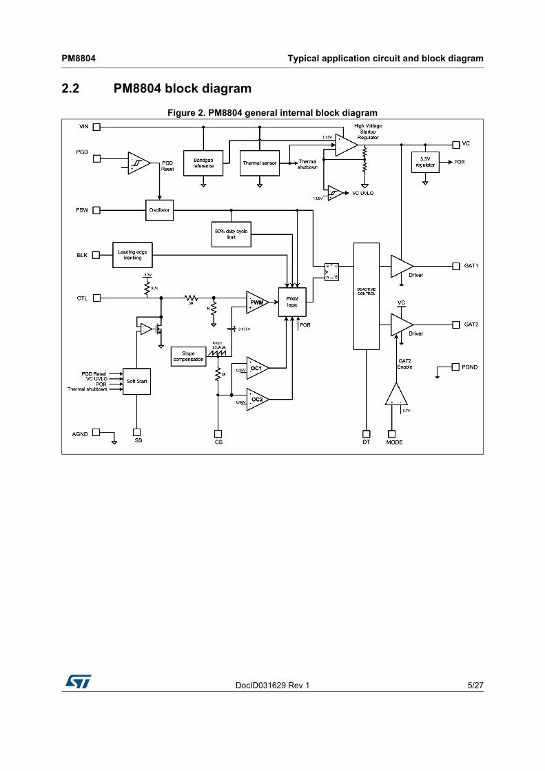
2.2 PM8804 block diagram
Figure 2. PM8804 general internal block diagram

Pins description and configuration PM8804
6/27 DocID031629 Rev 1
3 Pins description and configuration
Figure 3. Pins configuration (top view)
Table 2. Pin description
Pin no. Name Function
1 AGNDAnalog signal GND.
GND for all the sensitive analog circuitries. It must be connected to the PGND in a star ground configuration: a single connection point close to pin 10.
2 SSSoft-start set.A capacitor connected from this pin to AGND sets the converter soft-start time. Use of stable ceramic capacitors is recommended.
3 DTDelay time set.
A resistor connected from this pin to AGND sets the delay time between GAT1 and GAT2 in the range 10 ns to 200 ns. This pin cannot be left open
4 FSWSwitching frequency set.An external resistor connected from FSW to AGND can set the oscillator frequency in the range 100 kHz to 1 MHz.
5, 7 NCNot connected pin.
On layout leave this pin unconnected; in this way this increases the creepage distance between VIN and PGD pins and the other device pins.
6 PGD
Power Good, active high signal.
A low to high transition enable converter operation, typically a startup sequence. In case the PGD signal is de-asserted during normal operation, at the high to low transition the converter operation is stopped and both GAT1 and GAT2 signals are frozen in their default level state.
8 VINHigh-voltage input pin. Typically in PoE applications this voltage is the rectified voltage of input bridges and it is referred to AGND.
9 GAT1Main gate driver output of the PWM controller.
DC-DC converter gate driver output with 1 A peak sink -0.8 A source current capability. (5 typ. MOSFETs).
DocID031629 Rev 1 7/27
PM8804 Pins description and configuration
27
10 PGNDSystem power and analog ground. Power ground for the gate drivers.
This pin will be connected to AGND in a star ground configuration: a single connection point close to the pin 10. See more details in Section 6: Layout guidelines on page 21.
11 GAT2
Secondary gate driver output.
AUX gate driver output for active clamp or synchronous rectification designs. 1 A peak sink -0.8 A source current capability (5 typ. MOSFETs). Its time delay with respect to GAT1 signal can be adjusted through DT pin. The operation of GAT2 pin can be selected through MODE pin.
12 VC
Output of the internal high-voltage start up regulator.
When the voltage applied to VIN is powered up, the startup regulator charges the external capacitance up to 8 V typ. and a converter startup is attempted; Filter this pin with a ceramic capacitor connected to AGND; a 2.2 F, 25 V ceramic capacitor is typically enough to cover most of the applications.
13 MODE
Operation mode set.
Through this pin it is possible to select operation mode for the converter.
Connect this pin to AGND to turn off GAT2 when not used, and to disable the soft-stop feature. If left open, this pin is internally pulled up: GAT2 and soft-stop features are enabled.
14 CS
Current sense input for current mode control and overcurrent protection.
Current sensing is accomplished using a dedicated current sense comparator. If the CS pin voltage exceeds 0.25 V, the GAT1 pin switches low for cycle-by-cycle current limiting. CS is internally held low for a blanking period after GAT1 switches high to blank leading edge current spikes.
15 CTLThe input of the pulse width modulator (PWM) circuit.
CTL useful range is between 0.7 V and 1.7 V and a pull-up resistance of 3.3 k is integrated; this resistance may also be used to bias an optocoupler transistor in isolated applications.
16 BLK
Blanking time set.
An internal blanking time is integrated in order to prevent false overcurrent detection to terminate the PWM waveform. This is done after the rising edge of the primary side MOSFET. The masking time, active for a duration between 10 ns and 200 ns is set by a resistor placed between BLK and AGND.
- EPExposed pad. Connect this pad to a PCB copper plane to improve heat dissipation; it must be electrically connected to AGND.
Table 2. Pin description (continued)
Pin no. Name Function

Electrical specifications PM8804
8/27 DocID031629 Rev 1
4 Electrical specifications
4.1 Absolute maximum ratings
4.2 Thermal data
Table 3. Absolute maximum ratings
Parameter Value(1)
1. Absolute maximum rating is the limit beyond which may occur a permanent damage to the device. Exposure to absolute-maximum-rated condition for extended periods may affect device reliability.
Unit
VIN to AGND -0.3 to 85 V
VC to AGND -0.3 to 16 V
GAT1, GAT2 to PGND -0.3 to VC +0.3 V
MODE, DT, FSW, CTL, CS, BLK, SS to AGND -0.3 to 3.6 V
PGD to AGND -0.3 to VIN +0.3 V
ESD HBM 2 KV
ESD CDM 500 V
Maximum operating junction temperature -40 to 150 °C
Storage temperature -40 to 150 °C
Table 4. Thermal data
Symbol Parameter Value Unit
RTHJA Thermal resistance junction to ambient(1)
1. Package mounted on a 4 layers board (2 signals + 2 powers), Cu thickness 35 micron, with 5 x 5 via holes on the exposed pad copper area connected to each inner power plane of 1 x 1 inches minimum size.
30 °C/W
RTHJB Thermal resistance junction to board(1) 15 °C/W
Pd max Maximum power dissipation of device(2)
2. With device mounted on the board described in 1. and Ta = 85 °C.
1.3 W
TSTG Storage temperature range -40 to 150 °C
TJ Operative junction temperature range -40 to 125 °C
TA Operative ambient temperature range -40 to 85 °C

DocID031629 Rev 1 9/27
PM8804 Electrical specifications
27
4.3 Electrical characteristic
VIN = 48 V, VC = open, GAT1 and GAT2 = open, TA = -40 °C to 85 °C unless otherwise specified).
Table 5. Electrical characteristic(1)
Symbol Parameter Test conditions Min. Typ. Max. Unit
Input voltage VIN
VIN Input voltage VIN rising 10 - 75 V
Power Good PGD
PGDON Turn on threshold PGD rising 765 815 865 mV
PGDOFF Turn off threshold PGD fallingPGDON
-120PGDON
-100PGDON
-80mV
HV linear regulator VC(2)
VC
VCS, Internal default set
- 7.6 8.0 8.4 V
Regulator dropoutIC = 10 mA; GATE1, GATE2 = open
- 2.3 2.8 V
Current limit GATE1, GATE2 = open 13 22 31 mA
VConoff
Turn off threshold VC rising - 8.3 - V
Turn on threshold VC falling - 6.0 - V
VCUV
UVR, release VC rising 7.2 7.6 8 V
UVF, lock-out VC falling 4.75 5 5.25 V
VCOV OV, threshold VC rising 14.8 15.3 16.0 V
Oscillator FSW
FSW
Frequency accuracyIn the range from 100 to 500 kHz
- ±10 - %
Frequency Programmability
RFSW = 47 k 425 475 525 kHz
RFSW = 100 k 210 235 260 kHz
RFSW = 250 k 90 100 110 kHz
- Frequency range Typical value 100 - 1000 kHz
- Fsw voltage - 1.20 1.25 1.30 V
Delay time DT
-GATE1 to GATE2 delay time
RDT = 20 k GATE1 and GATE2 open
- 15 - ns
RDT = 390 k GATE1 and GATE2 open
- 195 - ns
- DT voltage - 1.20 1.25 1.30 V

Electrical specifications PM8804
10/27 DocID031629 Rev 1
Soft-start / soft-stop
TSS Soft-start timeCSS = 33 nF; over CTL full range (0.7 V to 1.7 V)(3) - 16.5 - ms
ISS_PRECHARGESoft-start pre-charge current
From SS = 0 V to SS = 0.7 V 8 10 12 A
TSS_PRECHARGESoft-start pre-charge delay
From SS = 0 V to SS = 0.7 V; CSS = 33 nF(3) - 2.3 - ms
ISS_CHARGE
Soft-start charge/discharge current
For SS > 0.7 V 1.3 2 2.7 A
ISS_DISCHARGESoft off discharge current
From CTL set point to 0.7 V 6.5 10 13.5 A
Blanking time BLK
- Blanking timeRBLK = 20 k - 15 - ns
RBLK = 390 k(3) - 195 - ns
- BLK voltage - 1.20 1.25 1.30 V
Current limit CS
- Delay to output (3) - 20 - ns
OC1THCycle by cycle current
Limit threshold voltage- 0.22 0.25 0.28 V
OC2TH4-times retry current Limit threshold voltage
- 0.32 0.35 0.38 V
-Slope compensation peak current
Sourced by CS pin at 80% duty cycle
17 21.5 26 µA
PWM comparator CTL
- Delay to output Guaranteed by design - 25 - ns
- Minimum duty cycle CTL = 0, CS = 0 - - 0 %
- Maximum duty cycleCTL = 2 V, CS = 0, FOSC = 250 kHz
75 80 85 %
- CTL to PWM gain (3) - 1:4 - -
- CTL operative range (3) 0.7 - 1.7 V
-Internal CTL pull-up resistance
To internal 3V3 ref. voltage 3 3.3 3.8 k
Table 5. Electrical characteristic(1) (continued)
Symbol Parameter Test conditions Min. Typ. Max. Unit

DocID031629 Rev 1 11/27
PM8804 Electrical specifications
27
Mode comparator
VTH_MODE_RMode rising threshold, VMR
MODE rising 750 800 850 mV
VTH_MODE_FMode falling threshold, VMF
MODE falling VMR - 120 VMR -100 VMR -80 mV
IOFF_MODE Input low output currentVMODE < VTH_MODE -VHYST_MODE
- 1 - A
Output driver GAT1 and GAT2
- Fall time CLOAD = 3.3 nF, VC = 10 V(3) - 40 - ns
- Rise time CLOAD = 3.3 nF, VC = 10 V(3) - 45 - ns
- Peak source current CLOAD = 3.3 nF, VC = 10 V(3) - 0.8 - A
- Peak sink current CLOAD = 3.3 nF, VC = 10 V(3) - 1 - A
Thermal shutdown
OTTH Shutdown temp. Always active(3) - 160 - °C
- Shutdown hyst. (3) - 30 - °C
Device current consumption
- VIN quiescent current VIN > VUVLO_R, VC = 10 V - 0.3 0.5 mA
- VC quiescent currentVIN > VUVLO_R, VC = 10 V, CTL = 3.3 V
- 1.2 1.5 mA
1. All devices are 100% production tested at TA = +25 NC. Limits overtemperature are guaranteed by design and correlation.
2. The VC regulator is intended for internal use only as startup supply of PM8804; any additional external VC current, like the external MOSFET driving current, has to be take in account in the dimensioning of the filter capacitor to be connected with VC pin; VC regulator cannot supply continuously the specified max current limit.
3. Parameter guaranteed by design.
Table 5. Electrical characteristic(1) (continued)
Symbol Parameter Test conditions Min. Typ. Max. Unit

Applications information PM8804
12/27 DocID031629 Rev 1
5 Applications information
5.1 High-voltage start-up regulator and VC pin
The device embeds a high-voltage startup regulator to provide the supply voltage to the internal current mode PWM controller during its startup phase and if needed, also during the normal operation.
The regulated voltage is typically 8 V and it is internally connected to the VC pin as well as to the controller section.
In normal isolated topology, the VC pin is diode-connected to the auxiliary winding of the transformer used for the flyback or forward configuration. When the voltage from the transformer exceeds the regulated voltage, the high-voltage regulator is shut off, reducing the amount of power dissipated inside the PM8804.
More in detail, when the auxiliary voltage surpasses 8.3 V, the HV regulator resets its regulation level to less than 6.0 V. In this way, a loosely regulated voltage from the external auxiliary supply is allowed without current-sharing with the internal regulator. If the auxiliary voltage drops under 6 V, the internal regulator is turned on in order to supply the controller and maintain the output regulation.
While the auxiliary voltage has to be higher than 8.0 V to take advantage of the auxiliary winding, it must be also lower than 15.3 V for all operating conditions, to avoid the intervention of the internal OV protection.
A ceramic capacitor at least 2.2 F must be connected at the controller output to guarantee the stability of the HV regulator.
For applications with high current drawn from VC pin, a large capacitance should be connected on VC pin in order to avoid converter switch-off during the startup phase.
A UV/OV mechanism monitors the level of voltage on the VC pin.
When VC voltage overcomes the UVLO rising threshold (VCUV_R), the PWM controller is enabled by the assertion of PGD signal and it remains enabled until the VC voltage drops below the UVLO falling threshold (VCUV_F) or the PGD is de-asserted. The VCUV_F is set to 5.0 V typically: below this voltage the PWM controller operations are stopped and the outputs frozen in default state.
The overvoltage circuitry detects a feedback fault condition on the output voltage by sensing the VC voltage. If VC exceeds the OV rising threshold (VCOV_R), the PWM controller is stopped, the soft-start capacitor discharged, then a new start up is attempted.
In case of persistent overvoltage, the control logic tries 4 cycles of fast hiccup before definitively shutting down the PWM controller. To restart the device the main supply VIN must be lowered to ground and then powered up again.
The HV regulator internal current limit is set at 22 mA typ. This value includes the current internally drawn to bias the controller, the gate drivers, and the external components that may be connected to the VC pin.
The use of an external auxiliary source is strongly recommended: the amount of power dissipated inside the device will be significantly reduced.
DocID031629 Rev 1 13/27
PM8804 Applications information
27
On the contrary using the internal HV regulator without the auxiliary winding increases the internal power dissipation, and in case of high ambient temperature and high power MOSFETs to drive, this may lead the device into thermal shutdown.
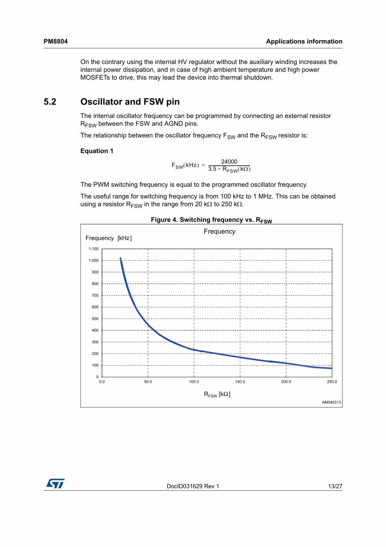
5.2 Oscillator and FSW pin
The internal oscillator frequency can be programmed by connecting an external resistor RFSW between the FSW and AGND pins.
The relationship between the oscillator frequency FSW and the RFSW resistor is:
Equation 1
The PWM switching frequency is equal to the programmed oscillator frequency.
The useful range for switching frequency is from 100 kHz to 1 MHz. This can be obtained using a resistor RFSW in the range from 20 k to 250 k.
Figure 4. Switching frequency vs. RFSW
FSW kHz 240003.5 RFSW k +-------------------------------------------=
Applications information PM8804
14/27 DocID031629 Rev 1
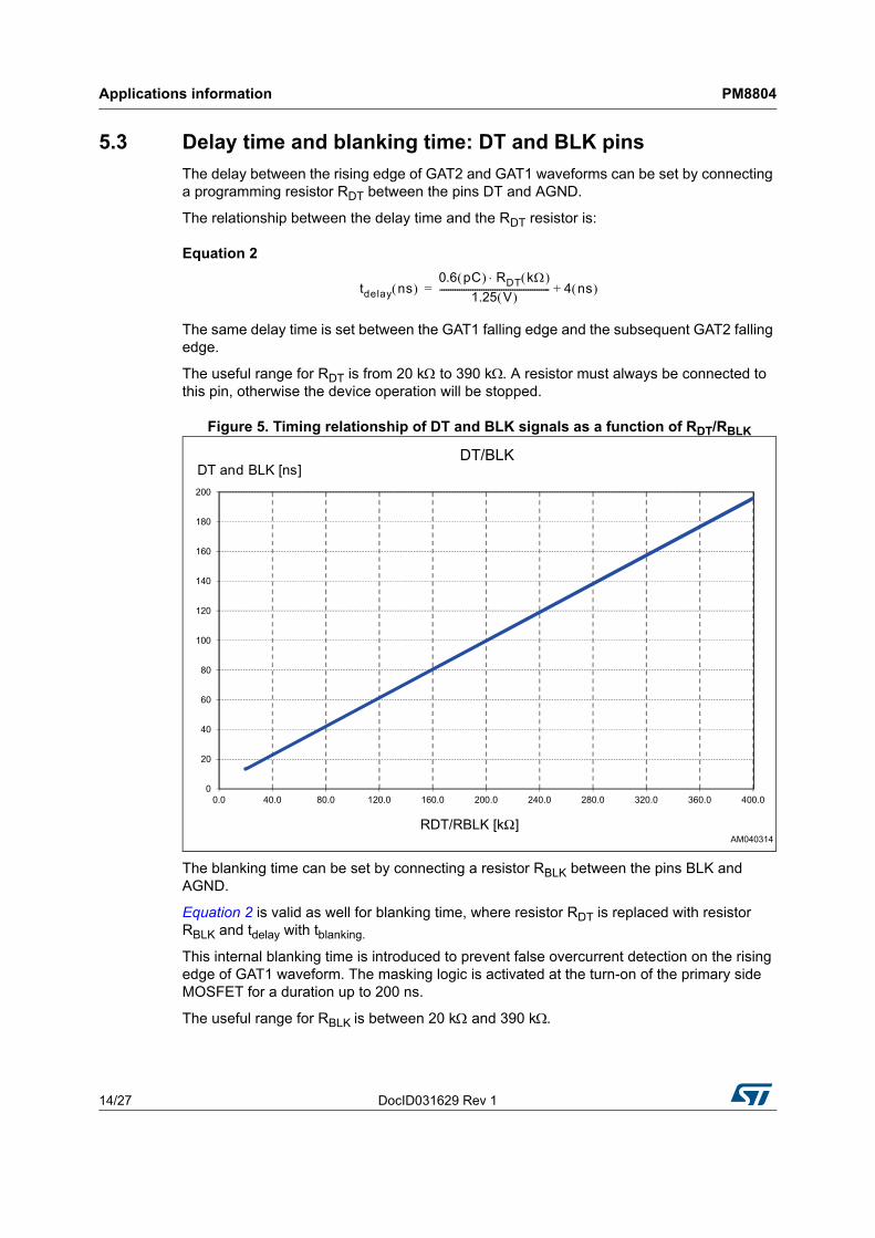
5.3 Delay time and blanking time: DT and BLK pins
The delay between the rising edge of GAT2 and GAT1 waveforms can be set by connecting a programming resistor RDT between the pins DT and AGND.
The relationship between the delay time and the RDT resistor is:
Equation 2
The same delay time is set between the GAT1 falling edge and the subsequent GAT2 falling edge.
The useful range for RDT is from 20 k to 390 k. A resistor must always be connected to this pin, otherwise the device operation will be stopped.
Figure 5. Timing relationship of DT and BLK signals as a function of RDT/RBLK
The blanking time can be set by connecting a resistor RBLK between the pins BLK and AGND.
Equation 2 is valid as well for blanking time, where resistor RDT is replaced with resistor RBLK and tdelay with tblanking.
This internal blanking time is introduced to prevent false overcurrent detection on the rising edge of GAT1 waveform. The masking logic is activated at the turn-on of the primary side MOSFET for a duration up to 200 ns.
The useful range for RBLK is between 20 k and 390 k.
tdelay ns 0.6 pC RDT k
1.25 V -------------------------------------------------- 4 ns +=

DocID031629 Rev 1 15/27
PM8804 Applications information
27
As for delay time, a resistor must always be connected to BLK pin, otherwise the device operation will be stopped. Values for DT and BLK must be selected to be compatible with the selected switching frequency; this constraint becomes more critical for high switching frequencies due to the reduced duration of pulses.
The following relation con be used as a general “rule of thumb”:
Equation 3
2 · DT + BLK ≤ 10% · TSW
In case of FSW = 500 KHz, TSW is 2 µs and assuming a duty cycle of 50%, the clock pulse lasts 1 µs. In order to satisfy Equation 3, two possible combination of DT and BLK are:
1. DT = 30 ns, BLK = 30 ns
2. DT = 20 ns, BLK = 50 ns
5.4 Soft-start / soft-stop and SS pin
The soft-start feature allows the output voltage to ramp-up in a safe and controlled way.
At the startup of the converter, the input voltage of the PWM comparator (CTL pin) is clamped to the SS pin voltage, which is progressively ramped-up until it reaches the regulation voltage. This results in a converter duty cycle increasing from zero to the operative value.
The voltage ramp on SS pin is achieved by charging an external CSS capacitor connected to the pin with a 2 µA internal current source.
Taking into account that the output voltage will start to rise only when the CTL voltage is higher than 0.7 V, the effective duration of the output voltage soft-start ramp can be estimated with the following formula:
Equation 4
The CTL voltage level depends on many factors: the topology, the converter working mode and the output capacitance. Typical values are in the range from 1 to 2 V. Assuming a mean value of CTL = 1.5 V and considering CSS = 33 nF, the resulting soft-start time will be about 13 mS.
Typical values for CSS are in the range 10 nF to 100 nF.
At the start-up, the baseline of 0.7 V on CTL is reached charging the soft-start capacitor with a 10 A current source. After the start-up phase, the SS voltage level is actively maintained at 2.3 V by an internal control circuitry, which also manages overcurrent and fault conditions.
In case of normal shutdown or thermal fault, the device features a soft-stop procedure. The soft-stop helps to reduce the stress and the overvoltages on the power MOSFET and it is achieved discharging slowly the soft-start capacitor with a 10 A current sink.
Except for thermal protection, the soft-stop is not applied for all the other fault conditions.
A summary is reported in Table 6. The soft-stop can be disabled connecting the MODE pin to AGND.
tSS ms CSS nF CTL V 0.7 V – 2 A
-------------------------------------------------=

Applications information PM8804
16/27 DocID031629 Rev 1
5.5 PWM comparator / slope compensation and CTL pin
In a typical isolated topology, the error amplifier is located outside the IC and the feedback signal is taken on the collector of an optocoupler, while the current is sensed through a sense resistor Rs connected between the source of the primary side MOSFET and the PGND pin.
The PWM comparator produces the PWM duty cycle by comparing the Rs ramp signal on CS with the error voltage derived from the error amplifier output.
The CTL voltage is internally pulled up to a fixed reference of 3.3 V using an internal 3.3 K resistor, and it is reduced by a 4:1 divider before being connected to the PWM comparator input.
The PWM duty cycle increases with the voltage at the CTL pin. The controller output duty cycle reduces to zero when the CTL pin voltage drops below approximately 0.7 V.
For duty cycles greater than 50%, current mode control loops are subject to sub-harmonic oscillation.
The device fixes the maximum duty cycle at 80% and implements a slope compensation technique consisting in adding a fixed slope voltage ramp to the signal at the CS pin. This is achieved by injecting a 21.5 µA saw tooth current into the current sense signal path on an integrated 2 k series resistor.
Additional slope compensation may be added by increasing the source impedance of the cur-rent sense signal connecting a resistor between the CS pin and the source of the current sense signal. The net effect is to further increase the slope of the voltage ramp at the PWM comparator terminals.
5.6 Current limit and CS pin
The current sensed through the CS pin is compared to two fixed levels of 250 mV and 350 mV.
The lower level of 250 mV is used to perform a cycle-by-cycle current limit, terminating the PWM pulse. In case of recurring overload a timing structure is activated through SS pin, sourcing a small current of about 2 µA on SS capacitor. The voltage on SS rises whenever during a PWM cycle an overcurrent event occurs, while decreases to the default voltage (2.3 V) if it does not.
Table 6. Fault management
Faults Reaction Turn off type
OV on VC 4 attempts then latched off state Fast turn off
OC2 4 attempts then latched off state Fast turn off
OvertemperatureThe device attempts a new soft-start only when the OT condition is removed
Soft-stop
UV on VCThe device attempts a new soft-start only when the VCUV rising threshold is passed again
Fast turn off

DocID031629 Rev 1 17/27
PM8804 Applications information
27
If SS voltage reaches 2.8 V, a slow hiccup is performed sinking 2 µA from SS, and shutting down the gate driver until the SS capacitor is fully discharged. Then a new soft-start procedure is performed.
When a severe overcurrent occurs, like a short-circuit of an internal power component, and 350 mV level is reached on CS, the gate driver is instantaneously shut down and a fast hiccup cycle is performed. When the 10 µA sink current fully discharges the SS capacitor, a new soft-start procedure with a charging current of 10 µA is performed.
In case of persistent severe overcurrent, the control logic tries 4 cycles of fast hiccup before definitively shutting down the PWM controller. To restart the device, after removing the cause of overcurrent, VIN must be lowered to ground and then powered up again.
Figure 6. Short-circuit on the power transformer output
Ch1= SS, Ch2 = VG1, Ch3 =VCS, Ch4 = Vsense
5.7 Output drivers: GAT1 / GAT2 and MODE pin
The PM8804 is integrating two MOSFET drivers with up to 1 A peak sink current capability.
GAT1 is intended for driving the main switching MOSFET, while GAT2 is used for an auxiliary function, depending on the topology selected: it can be used to drive a gate drive transformer in synchronous flyback topologies or to control a P-channel MOSFET referred to PGND in active clamp forward topologies.
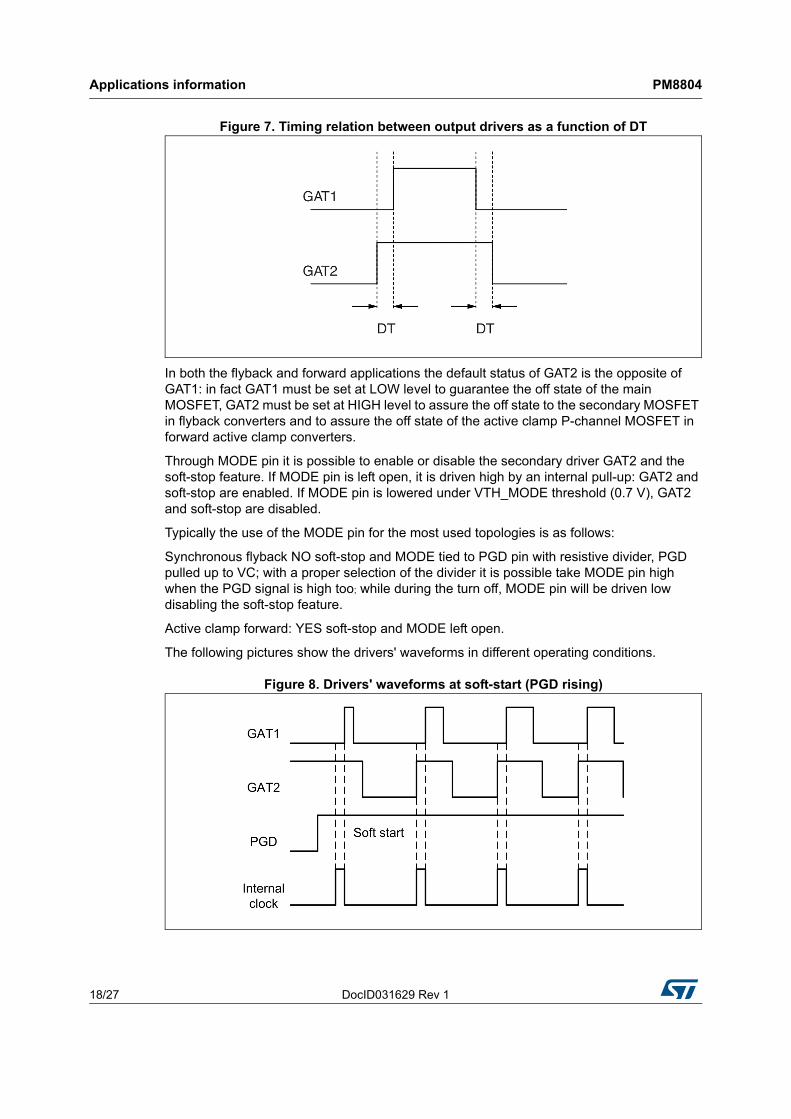
The rising edge of GAT2 is anticipated by time period DT with respect to the rising edge of GAT1, while the falling edge of GAT2 is delayed by the same time period DT with respect to the falling edge of GAT1 (see Figure 7).
DT can be adjusted from 10 ns to 200 ns to fine tune the relative switching times of the MOSFETs and to maximize the converter efficiency.
Applications information PM8804
18/27 DocID031629 Rev 1
Figure 7. Timing relation between output drivers as a function of DT
In both the flyback and forward applications the default status of GAT2 is the opposite of GAT1: in fact GAT1 must be set at LOW level to guarantee the off state of the main MOSFET, GAT2 must be set at HIGH level to assure the off state to the secondary MOSFET in flyback converters and to assure the off state of the active clamp P-channel MOSFET in forward active clamp converters.
Through MODE pin it is possible to enable or disable the secondary driver GAT2 and the soft-stop feature. If MODE pin is left open, it is driven high by an internal pull-up: GAT2 and soft-stop are enabled. If MODE pin is lowered under VTH_MODE threshold (0.7 V), GAT2 and soft-stop are disabled.
Typically the use of the MODE pin for the most used topologies is as follows:
Synchronous flyback NO soft-stop and MODE tied to PGD pin with resistive divider, PGD pulled up to VC; with a proper selection of the divider it is possible take MODE pin high when the PGD signal is high too; while during the turn off, MODE pin will be driven low disabling the soft-stop feature.
Active clamp forward: YES soft-stop and MODE left open.
The following pictures show the drivers' waveforms in different operating conditions.
Figure 8. Drivers' waveforms at soft-start (PGD rising)

DocID031629 Rev 1 19/27
PM8804 Applications information
27
Figure 9. Drivers' waveforms at soft-stop (PGD falling)
Figure 10. Drivers' waveforms when OCP1 is occurring
Figure 11. Drivers' waveforms when OCP2 is occurring

Applications information PM8804
20/27 DocID031629 Rev 1
Figure 12. Drivers' waveforms when a VCC fault is occurring
5.8 Thermal protection
The PM8804 thermal protection limit is set to 160 °C on the junction temperature and is always active. When this threshold is exceeded, the PWM controller is switched-off following the soft-stop method.
When the junction temperature goes below about 130 °C the converter will restart automatically doing a startup phase and without need to recycle the input voltage.

DocID031629 Rev 1 21/27
PM8804 Layout guidelines
27
6 Layout guidelines
6.1 General guidelines for 48 V converter
The following general guidelines are valid for all the typical converter topologies used for 48 V PoE/PoE+ converters.
The length of the interconnections between the following groups of components belonging to the primary side of the converter must be kept as short as possible:
1. Input ceramic capacitors
2. Input side of the power transformer
3. Power MOSFET and sense resistors
4. Active clamp circuitry or snubber circuitry (if present)
The length of the interconnections between the following groups of components belonging to the secondary side of the isolation must be kept as short as possible
1. Secondary rectifier diode(s), or synchronous rectifier MOSFET(s) and associated driving circuitry
2. Output side of the power transformer
3. Output ceramic capacitors
Isolation / spacing as required by applicable safety standards must be assured between all the rails / traces / planes at 48 V and between primary and secondary side of the converter.
Figure 13. PM8804 ground areas (top view)

Layout guidelines PM8804
22/27 DocID031629 Rev 1
6.2 How to layout the PM8804 ground pins
PM8804 is provided with two different pins of ground AGND and PGND plus an exposed pad.
The exposed pad must be connected to AGND and is recommended a fill area with at least a matrix of 3 x 3 vias to AGND plane.
Increase the number of AGND power planes helps improve the heat dissipation and it is recommended under the PM8804.
Is recommended to use a wide power copper plane for AGND connection and when is possible avoid to use traces.
The board ground must be separated into PGND and AGND: pin 11 and pin 9 must be referred to PGND; all other circuitry and all others components must be connected to AGND.
The AGND must be connected to PGND in one point only, and it has to be as much as possible close to the pin10.
It is recommended to use a small copper area for the PGND.
AGND can be a wide copper plane connecting the several components referred to it.
On secondary side is recommend to keep separated the power path of the power secondary GND (output side of transformer, secondary rectifier, output capacitors) from the feedback network GND, which will be connected only at the output capacitors side.
The low potential of PoE/48V voltage can be routed with a wide trace at the input and along the input filter, to become a copper plane close to the PM8804.
6.3 Thermal aspects
Design the primary MOSFET area with at least 6 - 9 vias of connection to the internal copper area.
Increase where possible the number of connected power planes, at least below the MOSFETs and diodes to improve the heat dissipation.
Design the secondary rectifier area with at least 6 - 9 vias of connection to the internal copper area.
The Thermal copper area has to be sized taking into account the thermal reason and its impact on EMI when placed under switching devices like power MOSFETs and diodes.
DocID031629 Rev 1 23/27
PM8804 Layout guidelines
27
6.4 Component placement
Place the PM8804 and all the related components close to each other; use both sides
Place all the feedback components close to each other, use both sides
Place the sense resistors close to the power MOSFET, if possible on the same side
Place the input ceramic capacitors close to the input side of power transformer, if possible on the same side
Place the primary snubber network close to the power transformer, on the bottom side
Place the rectifier diode or MOSFET close to the output side of the transformer, if possible on the same side
Place the secondary snubber network close to the rectifier diode or MOSFET, bottom side
Place the decoupling capacitors for VC close to the PM8804 pin 1
Place the components for FSW, DT and SS pins in a quiet area, separated as much as possible from the other signals
Use interconnections of at least 20 mils for the following PM8804 pins: GAT1, GAT2, VC.

Package information PM8804
24/27 DocID031629 Rev 1
7 Package information
In order to meet environmental requirements, ST offers these devices in different grades of ECOPACK® packages, depending on their level of environmental compliance. ECOPACK® specifications, grade definitions and product status are available at: www.st.com. ECOPACK® is an ST trademark.
7.1 VFQFPN 3.0x3.0x1.0 16L 0.5 mm pitch package information
Figure 14. VFQFPN 3.0x3.0x1.0 16L 0.5 mm pitch package outline

DocID031629 Rev 1 25/27
PM8804 Package information
27
Figure 15. VFQFPN 3.0x3.0x1.0 16L 0.5 mm pitch recommended footprint
Note: This footprint is able to ensure insulation up to 30 Vrms (according to CEI IEC-664-1).
The device must be positioned within 0.02 A B.
Table 7. VFQFPN 3.0x3.0x1.0 16L 0.5 mm pitch mechanical data
SymbolDimensions (mm)
Min. Nom. Max.
A 0.80 0.90 1.00
A1 0.00 0.02 0.05
A3 0.20 REF.
b 0.20 0.25 0.30
D 3.00 BSC
D1 1.50 BSC
D2 1.70 1.80 1.90
e 0.50 BSC
E 3.00 BSC
E1 1.50 BSC
E2 1.70 1.80 1.90
L 0.30 0.40 0.50
k 0.20 - -
N 16 6 -

Revision history PM8804
26/27 DocID031629 Rev 1
8 Revision history
Table 8. Document revision history
Date Revision Changes
22-March-2018 1 Initial release.

DocID031629 Rev 1 27/27
PM8804
27
IMPORTANT NOTICE – PLEASE READ CAREFULLY
STMicroelectronics NV and its subsidiaries (“ST”) reserve the right to make changes, corrections, enhancements, modifications, and improvements to ST products and/or to this document at any time without notice. Purchasers should obtain the latest relevant information on ST products before placing orders. ST products are sold pursuant to ST’s terms and conditions of sale in place at the time of order acknowledgement.
Purchasers are solely responsible for the choice, selection, and use of ST products and ST assumes no liability for application assistance or the design of Purchasers’ products.
No license, express or implied, to any intellectual property right is granted by ST herein.
Resale of ST products with provisions different from the information set forth herein shall void any warranty granted by ST for such product.
ST and the ST logo are trademarks of ST. All other product or service names are the property of their respective owners.
Information in this document supersedes and replaces information previously supplied in any prior versions of this document.
© 2018 STMicroelectronics – All rights reserved