Improved Cosine Mode Current Controllers
3
552 IEEE TRANSACTIONS ON INIIUSTRIAL ELECTRONICS, VOL. 42, NO. 5 . OCTOBER 1995 Letters to the Editor An Improved Cosin e-Mode Controller for SCR Converters Yu-Kang Lo and Chem-Lin Chen Abstract- An improved cosine-mode controller for silicon-controlled rectifier (SCR) converters is presented. The proposed schem e linearizes the inpuvoutput transfer function of SCR converters. The replacement of monostables by AND gates i n the controller eliminates false tum- on s due to bouncings inside analog comparators. Experiments have been performed and satisfactory results are recorded. I. INTRODUCTION SCR converters are simple, inexpensive, and reliable. They are widely used in the industry, especially for high-power ac-to-dc rec- tification. Conventional SCR control uses direct firing angle control [ 11, which results in nonlinear control characteristics. This situation is undesirable in systems demanding high control performance, such as for dc magnet power supplies in a beam line system [2 ] and in superconducting and accelerator applications [3], 4]. To acquire linear control characteristics, the most common ap- proach is the cosine-mode control scheme. This scheme uses an indirect control variable as a substitute for firing angle [5], [6]. he transfer gain of this variable is made constant over the entire operating range. In this way, linear transfer characteristics of the compensated controller can be obtained. Upon implementing the cosine-mode controller, monostables are normally used to detect the outputs of analog comparators and pro- duce triggering signals. Owing to the high sensitivity of comparators composed of high-gain operational amplifiers, output bouncings are very likely to appear. Hence false triggering signals for SCR's may be generated at unexpected instants. In this letter, an improved method is presented for implementing a cosine-mode controller. Monostables are replaced by AND gates and undesirable bouncings are blocked by the "AND' process. Therefore, bouncings of comparator outputs will not disturb the generation of triggering signals. In the following sections, the cosine-mode control for various types of SC R converters are discussed and experimental results of a SCR semiconverter using the proposed controller are shown. 1 1 COSINE-MODE ONTROL FOR SCR CONVERTERS DC output voltage of a SCR converter, VO, s normally controlled by its firing angle, a , as VO = $ f(a), here V , s the amplitude of the ac input. f(a) s a nonlinear function and may take different forms for different converter topologies. Table I gives four common SCR converter topologies and their associated transfer function. For high-performance applications, there exists a problem with this type of control function. Its incremental gain, 2 , pproaches zero near maximum or zero dc output voltage. Manuscript received May 7, 1994; revised October 3, 1994 and May 1, The authors are with the Department of Electrical Engine ering, National IEEE Log Number 9413760. 1995. Tai wan University, Taipei, Ta iwan 10764, R.O.C. TABLE I FOUR CR COVVEWrER TOPOLOGIES ND THEIR RANSFER WCTtONS The cosine-mode control scheme is used to linearize the nonlinear control characteristic. A new control variable U , is defined as v = f(a). n this way, the output voltage 1 0 equals 2 . v Then a constant control gain over the entire operation range can be obtained by controlling tmrr directly. Taking a single-phase SCR semiconverter for example, f(a) = 1 + COSQ, fo r 0 < Q < 7r . By comparing V , with f(cu), the triggerings will commence at where f(m) equals ve . That is, the firing angle a is cos-'(v, - 1) for SCR l in the positive half- cycle and 7 r + cos-'(v, - 1) or cos-'(l - U , ) for SC 2 in the negative half-cycle. Substituting a into CY), we obtain 1 = $.vm, which features a constant gain of the dc output voltage to the control input. The basic control block diagram of the conventional approach is shown in Fig. ](a). A scaled voltage, v, , of the ac input is first integrated into a cosine signal U b . Two signals U,(= 1 + U b ) an d Ud(= 1 - V b ) are generated through a peak detector and an inverter. These voltages are then compared to the new control variable U , , to produce z e an d v f , which are two pulses commencing at d cy an d uf = a '. Monostables are used to detect the rising edge of v e an d 7)f to produce t i g an d v h with programmable width [6]. These signals trigger a SR fli p flop to generate signals and 0 3 . B y ANDing with a high-frequency oscillator (10-30 kHz), the effective triggerings are fed to fire the SCR's in the positive and negative half cycles, respectively. The timing diagram is shown in Fig. 2. Because of the highly noise-sensitive characteristic of operational amplifiers, there may be more than one intersection at the crossings of the two input signals. Thus the triggerings would be mistaken if the inevitable bouncings of the comparators' outputs are not carefull y handled. According to the timing diagram of Fig. 2, SCRl and SCR2 should be turned on at Q an d Q' , respectively, provided that the monostable circuits can correctly detect the rising edges of the triggering pulsex. Chances are that the monostables may detect a rising signal at ;I falling edge, say, at a", because of the bouncing problem of the comparators. This may result in the false "ON' signal for SC Rl in the very beginning of next positive half-cycl e; see i : ; an d U:. Thus S( 'R1 will conduct in the whole half-cycle and loose the function of power control. Comparators with Schmitt triggers help lower the sensitivity to noises. Ho wever, it is impractical to set a large hysteresis window in a highly noisy environment. In the modified approach, the monostables are replaced by a zero- crossing detector (ZCD) and AND gates. The ZCD is to detect source voltage polarity, hence its effectiveness will not be deteriorated by source distortion. Fig. l(b) describes the improved cosine-mode 0278-0046/95$04.00 0 1995 IEEE Authorized license d use limited to: National Taiwan University. Downloaded on February 25, 2009 at 02:41 from IEEE Xplore. Restrictions apply.
-
Upload
sougata-das -
Category
Documents
-
view
223 -
download
0
Transcript of Improved Cosine Mode Current Controllers
8/8/2019 Improved Cosine Mode Current Controllers
http://slidepdf.com/reader/full/improved-cosine-mode-current-controllers 1/3
552 IEEE TRANSACTIONS ON INIIUSTRIAL ELECTRONICS, VOL. 42, NO. 5 . OCTOBER 1995
Letters to the Editor
An Improved Cosine-Mode Controller for SCR Converters
Yu-Kang Lo and Chem-Lin Chen
Abstract- An improved cosine-mode controller for silicon-controlledrectifier (SCR) converters is presented. The proposed schem e linearizesthe inpuvoutput transfer function of SCR converters. The replacemen tof monostables by AND gates in the controller eliminates false tum-ons due to bouncings inside analog comparators. Experiments have beenperformed and satisfactory results are recorded.
I. INTRODUCTION
SCR converters are simple, inexpensive, and reliable. They are
widely used in the industry, especially for high-power ac-to-dc rec-
tification. Conventional SCR control uses direct firing angle control
[11, which results in nonlinear control characteristics. This situationis undesirable in systems demanding high control performance, such
as for dc magnet power supplies in a beam line system [2] and in
superconducting and accelerator applications [3], 4].
To acquire linear control characteristics, the most common ap-
proach is the cosine-mode control scheme. This scheme uses an
indirect control variable as a substitute for firing angle [ 5 ] , [6]. he
transfer gain of this variable is made constant over the entire operating
range. In this way, linear transfer characteristics of the compensated
controller can be obtained.
Upon implementing the cosine-mode controller, monostables are
normally used to detect the outputs of analog comparators and pro-
duce triggering signals. Owing to the high sensitivity of comparators
composed of high-gain operational amplifiers, output bouncings arevery likely to appear. Hence false triggering signals for SCR's may
be generated at unexpected instants.
In this letter, an improved method is presented for implementing a
cosine-mode controller. Monostables are replaced by AND gates and
undesirable bouncings are blocked by the "AND' process. Therefore,
bouncings of comparator outputs will not disturb the generation of
triggering signals. In the following sections, the cosine-mode controlfor various types of SC R converters are discussed and experimental
results of a SCR semiconverter using the proposed controller are
shown.
11 COSINE-MODEONTROL FOR SCR CONVERTERS
DC output voltage of a SCR converter, VO,s normally controlled
by its firing angle, a , asVO
= $ f(a), here V , s the amplitudeof the ac input. f(a) s a nonlinear function and may take different
forms for different converter topologies. Table I gives four common
SCR converter topologies and their associated transfer function. For
high-performance applications, there exists a problem with this type
of control function. Its incremental gain, 2 , pproaches zero near
maximum or zero dc output voltage.
Manuscript received May 7, 1994; revised October 3, 1994 and May 1,
The authors are with the Department of Electrical Engineering, National
IEEE Log Number 9413760.
1995.
Taiwan University, Taipei, Taiwan 10764, R.O.C.
TABLE I
FOURCR COVVEWrER TOPOLOGIESND THEIR RANSFERWCTtONS
The cosine-mode control scheme is used to linearize the nonlinear
control characteristic. A new control variable U , is defined as v =
f(a).n this way, the output voltage 10 equals 2 . v Then a
constant control gain over the entire operation range can be obtained
by controlling tmrr directly.Taking a single-phase SCR semiconverter for example, f ( a )=
1 + CO SQ , fo r 0 < Q < 7r . By comparing V, with f ( c u ) , the
triggerings will commence at where f(m) equals ve . That is, the
firing angle a is cos-'(v, - 1) for S C R l in the positive half-
cycle and 7r + cos-'(v, - 1) or cos-'(l - U,) for S C R 2 in the
negative half-cycle. Substituting a into CY), we obtain 1 = $ . v m ,
which features a constant gain of the dc output voltage to the control
input.
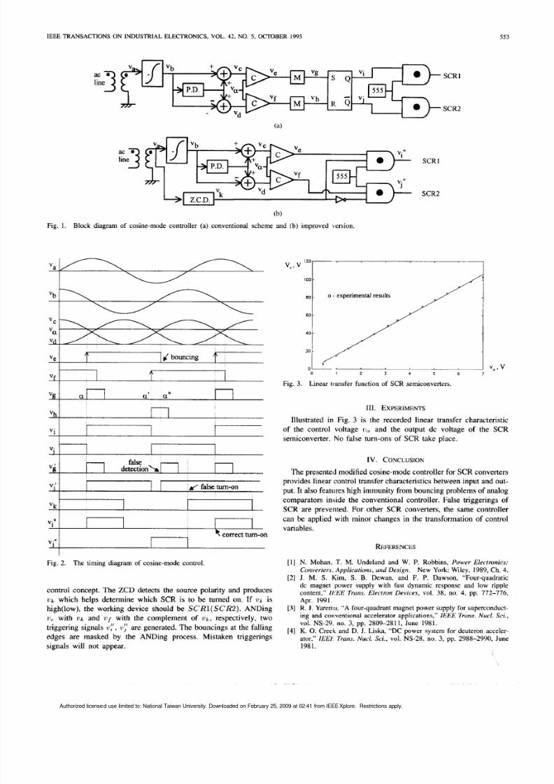
The basic control block diagram of the conventional approach is
shown in Fig. ](a). A scaled voltage, v,, of the ac input is first
integrated into a cosine signal U b . Two signals U,(= 1+ U b ) and
U d ( = 1- V b ) are generated through a peak detector and an inverter.
These voltages are then compared to the new control variable U , , to
produce ze and v f , which are two pulses commencing atd cy anduf = a'. Monostables are used to detect the rising edge of ve and 7)f
to produce tig and v h with programmable width [6]. These signals
trigger a SR fli p flop to generate signals and 0 3 .B y ANDing with
a high-frequency oscillator (10-30 kHz), the effective triggerings
are fed to fire the SCR's in the positive and negative half cycles,respectively. The timing diagram is shown in Fig. 2. Because of the
highly noise-sensitive characteristic of operational amplifiers, there
may be more than one intersection at the crossings of the two input
signals. Thus the triggerings would be mistaken if the inevitable
bouncings of the comparators' outputs are not carefully handled.
According to the timing diagram of Fig. 2, S C R l and S C R 2
should be turned on at Q and Q' , respectively, provided that themonostable circuits can correctly detect the rising edges of the
triggering pulsex. Chances are that the monostables may detect arising signal at ;I falling edge, say, at a", because of the bouncing
problem of the comparators. This may result in the false "ON' signal
for S C R l in the very beginning of next positive half-cycle; see i:;
and U : . Thus S( 'R1 will conduct in the whole half-cycle and loose
the function of power control. Comparators with Schmitt triggers help
lower the sensitivity to noises. Ho wever, it is impractical to set a large
hysteresis window in a highly noisy environment.
In the modified approach, the monostables are replaced by a zero-
crossing detector (ZCD) and AND gates. The ZCD is to detect
source voltage polarity, hence its effectiveness will not be d eterioratedby source distortion. Fig. l(b) describes the improved cosine-mode
0278-0046/95$04.00 0 1995 IEEE
Authorized licensed use limited to: National Taiwan University. Downloaded on February 25, 2009 at 02:41 from IEEE Xplore. Restrictions apply.
8/8/2019 Improved Cosine Mode Current Controllers
http://slidepdf.com/reader/full/improved-cosine-mode-current-controllers 2/3
IEEE TRANSACTIONS ON INDUSTRIAL ELECTRONICS, VOL. 42, NO. 5, OCTOBER 1995
Vf
553
t
line“3
V.’
.J false tum-o n
line“3
Vlll
V,‘I
+
+ corzect turn-onm
SCRl
SCR2
Fig. 1. Block diagram of cosine-mode controller (a) conventional scheme and (b) improved iersion.
IIIFig. 2. The timing diagram of cosine-mode control
control concept. The ZCD detects the source polarity and produces
Il k which helps determine which SC R is to be turned on. If ‘V I ishigh(low), the working device should be SCRl(SCR2).ANDing
7’, with UI; and u f with the complement of L‘L, respectively, tw o
triggering signals U:’, U:’ are generated. The bouncings at the fallingedges are masked by the ANDing process. Mistaken triggerings
signals will not appear.
SCRl
SCR2
100 -
EO -
60 -
40 -
20
0 I L _ I m , v0 1 2 3 4 5 6 7
Fig. 3. Linear transfer function of SCR semiconverters.
111. EXPERIMENTS
Illustrated in Fig. 3 is the recorded linear transfer characteristic
of the control voltage tiol and the output dc voltage of the SC R
semiconverter. No false turn-ons of SC R take place.
IV . CONCLUSION
The presented modified cosine-mode controller for SC R convertersprovides linear control transfer characteristics between input and out-
put. It also features high immunity from bouncing problems of analog
comparators inside the conventional controller. False triggerings of
SC R are prevented. For other SC R converters, the same controller
can be applied with minor changes in the transformation of control
variables.
REFERENCES
[ I ] N. Mohan, T. M. Undeland and W . P. Robbins, Power Electronics:Converters. Applications, and Design . New York: Wiley, 1989,Ch. 4.
[2] J. M. S . Kim, S . B. Dewan, and F. P. Dawson, “Four-quadraticdc magnet power supply with fast dynamic response and low ripple
content,” IEEE Trans. Electron Devices, vol. 3 8 , no. 4, pp . 772-776,
Apr. 1991.[3] R. J. Yarema, “A four-quadrant magnet power supply for superconduct-
ing an d conventional accelerator applications,” IEEE Trans. Nucl. Sci.,vol. NS-29. no. 3, pp . 2809-2811, June 1981.
[4] K. 0. Creek an d D. J. Liska, “D C power system for deuteron acceler-ator,” IEEt - Trans. Nucl. Sci., vol. NS-28, no. 3, pp . 2988-2990, June1981.
Authorized licensed use limited to: National Taiwan University. Downloaded on February 25, 2009 at 02:41 from IEEE Xplore. Restrictions apply.

8/8/2019 Improved Cosine Mode Current Controllers
http://slidepdf.com/reader/full/improved-cosine-mode-current-controllers 3/3
554 IEEE TRANSACTIONS ON INDUSTRIAL ELECTRONICS, VOL. 42, NO. 5 , OCTOBER 1995
[5] J. G.Kassakian, M . F. Schlecht,an d G . C. Verghese, Principles of PowerE k t r o n i c s . Reading, MA : Addison Wesley, 1991, Ch. 5, pp. 82-83.
[6 ] P. C. Sen, Thyristor DC Drives. New York Wiley, 1981, AppendixB, pp. 292-294.
A PSPICE Model for the MOS Controlled Thyristor
S . Yuvarajan and Danny Quek
Ahtract-A PSPICE model for the MOS Controlled Thyristor (MCT)consisting of an SCR section, and two MOSFET sections is proposed. Theparameters of the equivalent circuit are calculated from the data providedby the manufacturer and some simple measurem ents.The simulation andexperimental results of a phase-controlled rectifier are compared.
I. INTRODUCTION
The MOS Controlled Thyristor (MCT) is a new power semicon-ductor device having several advantages compared to other devices
[ l ] , [ 2 ] . The operating characteristics of the MCT have been studied
in the recent years [ 3 ] ,141. The MCT has a main SCR section, and
a gate control section for turning it on and off. Since the integration
of the MCT is complex, it is very difficult to obtain an exact circuit
model for the device. A simpler model for the MCT will help to
keep the simulation time and effort minimal. It is possible to develop
a model for the MCT by expanding the model of an SCR [ 5 ] , [6].
The paper presents a simple circuit model for the M CT w hich can
be used to analyze MCT power converters. The model represents
the characteristics of an MCT during turn-on and turn-off, and
it is developed from the transistor level equivalent circuit of the
MCT. Some of the features of the existing SCR models are used in
developing the proposed model of‘the MCT. The model parameters
are obtained from the specifications contained in the manufacturer’sdata sheet and some simple measurements on the MCT. The com plete
circuit of a phase-controlled rectifier is simulated using PSPICE
and the simulated responses are compared with the experimental
responses.
11. CIRCUIT MODEL OR THE MCT
The circuit model for the MCT is derived from the transistor-
level equivalent of the MCT shown in Fig. ](a). The MCT has an
SCR section with 91 an d Q2 and a gate control section with a
PMOSFET and an NMOSFET. In the proposed model of the MCT
in Fig. l(b), the SC R section is modeled by the diodes D A , Dc, an d
DJ,-nd the current-controlled current source (CCCS) FPNPY6].
The voltage controlled switch SP ntegrated into the model represents
the triggering action of the SCR within the MCT. A pair of controlled
current sources FP an d Gp is responsible for turning the MCT on
or off.
Manuscript received May 14, 1994; revised October 3, 1994 and Ma y 20,
The authors are with the Electrical Engineering Department, North Dakota
IEEE Log Number 9413761.
1995.
State University, Fargo, ND 58105 USA.
When a negative pulse is applied to the gate of the PMOS, the
capacitor CPMO, harges up. The voltage VPMOSacross CPMOS
increases the value of Fp which charges the capacitor C p . Th e
rapidly nsing voltage across RP an d Cp causes the resistance of
Sp to decrease from R,R to R,,, hereby establishing a path for the
anode current to flow. The current source FPNPNcross the diode
DC allows a current to flow from anode to cathode. It is expressed
as [61
FPNPNI ( V , )+ 0.951(& ) .
Once the MCT is turned on, with a positive voltage applied to the
anode, the anode current flows. The resistance of S p remains at the
low value Ron. The current ~ ( V K )elps to establish Gp and to
sustain conduction in the absence of a gate pulse. Once a positive
pulse is applied to the gate, the capacitorCNMos charges to a voltage
VNMOSwhich reduces the value of the current F p . The voltage across
the capacitor CIS educes, causing the resistance of S p o increase
to Raft..Thus the MCT is turned off. Once the device current falls tozero, the value ot FPNPYecomes zero thereby restoring the reverse-
connected diode DC into the circuit. The polynomial expressions for
F p an d Gp are given by
where V ~ M O Snd VNMOS re the MOSFE T capacitor voltages con-
tributing to the turning-on and turning-off of the MCT, respectively.
The coefficients PI an d P2 decide the relative contribution of the
two MO SFET voltages in turning the MCT on or off. The coefficient
Pj represents the latching action in the SCR section. The diodes
D p h IO , an d Dpv~os re used to isolate the operation of the PMOS
and NMOS such that the triggering pulse of one polarity activates
only one FET. The resistances RGP nd RGN ontrol the turn-on
delay and turn-off delay, respectively. The resistances RDP nd R ~ N
control the dis chu ge of the gate capacitors. The model of the M CT is
described in the lorm of a “subcircuit” given in Appendix A where the
quantities within the brackets ({ }) represent the numerical values to
be supplied.
111. DETERMINATION OF MODELPARAMETERS
Appendix B contains some of the electrical characteristics of the
MCT taken from the manufacturer’s data sheet [ 7 ] . The MCT is
connected as a dc chopper with an R-L load and driven by a square
wave. The following response times for anode current are accurately
measured using a digital storage oscilloscope:
turn-on delay ( f d o n ) = 0.3 p s ;rise time (fr,) = 0.2 p s
turn-off delay (&E) = 0.5 p s ;
fall time ( t f i )= 0.4 p s. (4)
The calculation of model parameters involves the following steps.
Step I : Calculation of R,, an d R,E: The on-resistance of Sp,
R,, is chosen to model the resistance of the MCT during conduction.
The value of R,,, is calculated as R,, = VTM/ITC.- Rx where
0278-0046/95$04.00 0 995 IEEE
Authorized licensed use limited to: National Taiwan University. Downloaded on February 25, 2009 at 02:41 from IEEE Xplore. Restrictions apply.