Enhanced oucoupling efficiency with nanostructured anodes
12
Richard Pfeifer, Karsten Fehse, Uwe Vogel, and Karl Leo 09.10.2012 © Fraunhofer COMEDD Fraunhofer Research Institution for Organics, Materials and Electronic Devices COMEDD Enhanced outcoupling efficiency with nanostructured anodes for OLED microdisplay integration
Transcript of Enhanced oucoupling efficiency with nanostructured anodes

Richard Pfeifer, Karsten Fehse, Uwe Vogel, and Karl Leo
09.10.2012
© Fraunhofer COMEDD
Fraunhofer Research Institution for Organics, Materials and Electronic Devices
COMEDD
Enhanced outcoupling efficiency with
nanostructured anodes for OLED microdisplay
integration
© Fraunhofer COMEDD
Richard Pfeifer I 09.10.2012 I slide 2
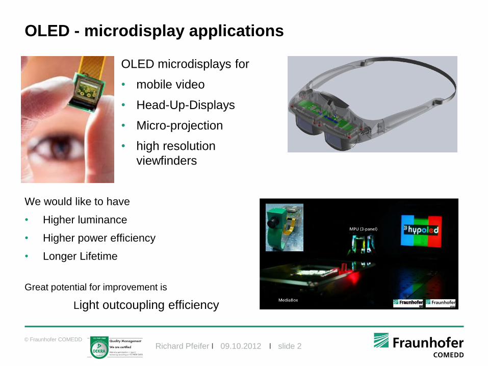
OLED - microdisplay applications
We would like to have
• Higher luminance
• Higher power efficiency
• Longer Lifetime
Great potential for improvement is
Light outcoupling efficiency
OLED microdisplays for
• mobile video
• Head-Up-Displays
• Micro-projection
• high resolution
viewfinders

© Fraunhofer COMEDD
Richard Pfeifer I 09.10.2012 I slide 3
Outline
• Enhanced light outcoupling by gratings
• Integration of gratings into OLED-stacks
• Grating parameters
• Simulation model
• Results
• Conclusion

© Fraunhofer COMEDD
Richard Pfeifer I 09.10.2012 I slide 4
Enhanced light outcoupling by gratings
Waveguided modes
(total interal reflection)
Surface Plasmon Polaritons
(evanescent excitation)
Radiating modes
Nonradiating decays
Planar OLED: Light emitted into waveguide modes is lost
emitting layer
Cathode
Anode
Substate
Leaky Waveguide modes
(by grating coupling)
Surface Plasmon Polaritons
(evanescent excitation)
Radiating modes
Nonradiating decays
emitting layer
Cathode
Anode
Substate
Grating OLED: Waveguide modes are „leaky“

© Fraunhofer COMEDD
Richard Pfeifer I 09.10.2012 I slide 5
Gratings and Microdisplays: A perfect match?
Usage of gratings fabricated by optical lithography favorable because
•Small active area
•Fabrication process does already involve multiple CMOS processes
•Integration into high value products
•Demand for high luminance
•Homogeneity no strict necessity in terms of
• Angular dependance
• White light appearance

© Fraunhofer COMEDD
Richard Pfeifer I 09.10.2012 I slide 6
Grating integration
• Microdisplays use top-emitting OLEDs:
• How to integrate gratings into thin-film stacks?
• without disturbing electrical properties of OLED
• Exposing OLED to harmful conditions
• Use CMOS-processes already available for active
matrix backplane fabrication
Metal cathode
Organic stack
Grating: conductive high index material (e.g. Si) /
low index material (SiO2)
Planar conductive high index layer (e.g. Si)
Metal anode

© Fraunhofer COMEDD
Richard Pfeifer I 09.10.2012 I slide 7
Simulations • Model: dipole emitters embedded in thin-film stacks [1]
• Light emitted into different angles is independent
no coupled modes
• Fast calculation of
• power emitted into each mode at position of emitter
• power in modes above thin film structure
Get outcoupling efficiency
• Calculate ‚outcoupling enhancement factor‘ OEF along kx-direction
• Modes differing by grating vector 2π/a are coupled
• Using RCWA [2] to calculate power into coupled modes.
• choose symmetric emitter position
• integration along - direction (restrict to direction of
greatest influence)
[1] RR Chance, A Prock, R Silbey ;The Journal of Chemical Physics, 1974
[2] MG Moharam, EB Grann, DA Pommet, TK Gaylord, JOSA A, Vol.12 No 5, 1995
RCWA…”Rigorously Coupled Wave Analysis”
top view side view
kx
top view
kx
kax
ax
side view

© Fraunhofer COMEDD
Richard Pfeifer I 09.10.2012 I slide 8
Planar OLED vs grating OLED
best outcoupling
efficiency (OCE): 29.2%
height grating: 50nm
height planar layer: 60nm
grating period a: 280nm
Simulated stack: green p-i-n OLED at 525nm
Grating: nlow=1.48 nHigh=4.19+0.007i (k comparable to organic)
ETL
HTL
grating
planar
layer
outcoupling
enhancement factor
(OEF) : 1.43

© Fraunhofer COMEDD
Richard Pfeifer I 09.10.2012 I slide 9
Influence of grating period
Parameter variation
• HTL 20 … 80nm
• ETL 30 … 80nm
• Grating 40 … 70nm
• Planar 40… 70nm
• Period 225…405nm
-> 220.000 datapoints
• Correlation between grating period and optical cavity length for highest OEF
• grating period determines kt of outcoupled waveguide mode
• kt of waveguide modes determined by optical length of cavity s

© Fraunhofer COMEDD
Richard Pfeifer I 09.10.2012 I slide 10
Influence of absorption
• Light absorption of silicon lowers outcoupling enhancement factor in optical
wavelength range
• Silicon as available high-index material in typical CMOS-foundries has higher
exctinction coefficient
-> effect for grating: 50nm, planar: 50nm, HTL: 40nm
k=0.007 (organic) k=0.011
k=0.020 (Si@620nm) k=0.034 (Si@525nm)

© Fraunhofer COMEDD
Richard Pfeifer I 09.10.2012 I slide 11
Conclusion
• Gratings and Microdisplays:
• Demonstrated concept for integration of high-index-contrast grating into
thin-film stack
• Grating concept only depends on CMOS processes and materials already
available for active matrix backplane fabrication
• Used RCWA-based simulation to evaluate beneficial grating parameters
• Real world extinction coefficient of silicon lowers outcoupling efficiency
enhancement in optical region of spectrum
• More flexibility of allowed materials needed (e.g. TCOs)
• Address infrared applications

© Fraunhofer COMEDD
Richard Pfeifer I 09.10.2012 I slide 12
Acknowledgments
This work has been partly funded with support from the Free State of Saxony and
the European Commission (EFRE) within the project CoolProjektor.