REVIEW Designing nanostructured Si anodes for high … · · 2013-12-05REVIEW Designing...
16
Nano Today (2012) 7, 414—429 Available online at www.sciencedirect.com journal homepage: www.elsevier.com/locate/nanotoday REVIEW Designing nanostructured Si anodes for high energy lithium ion batteries Hui Wu a , Yi Cui a,b,∗ a Department of Materials Science and Engineering, Stanford University, Stanford, CA 94305, USA b Stanford Institute for Materials and Energy Sciences, SLAC National Accelerator Laboratory, 2575 Sand Hill Road, Menlo Park, CA 94025, USA Received 21 May 2012; received in revised form 23 July 2012; accepted 17 August 2012 Available online 30 September 2012 KEYWORDS Lithium ion battery; Si nanostructures; Anodes; Electrochemistry; Solid electrolyte interphase Summary High energy lithium ion batteries are in demand for consumer electronics, electric- drive vehicles and grid-scale stationary energy storage. Si is of great interest since it has 10 times higher specific capacity than traditional carbon anodes. However, the poor cyclability due to the large volume change of Si upon insertion and extraction of lithium has been an impediment to its deployment. This review outlines three fundamental materials challenges associated with large volume change, and then shows how nanostructured materials design can successfully address these challenges. There have been three generations of nanostructure design, encompassing solid nanostructures such as nanowires, hollow nanostructures, and clamped hollow structures. The nanoscale design principles developed for Si can also be extended to other battery materials that undergo large volume changes. © 2012 Elsevier Ltd. All rights reserved. Introduction Rechargeable batteries have been critical for enabling portable consumer electronics and are beginning to be used in electric vehicles. They are also becoming an attractive option for large-scale stationary energy storage [1—6]. For mobile applications, high energy (per weight and volume) is the most important parameter since it determines the usage time per charge [4]. For stationary applications, cost is the most important design parameter, and high energy batteries could help reduce the cost per unit of stored energy [1,7,8]. ∗ Corresponding author. Tel.: +1 650 723 4613. E-mail address: [email protected] (Y. Cui). Therefore, obtaining high energy density has been a major focus of recent battery research. Compared to other technologies, lithium-ion batteries (LIBs) are the most popular rechargeable batteries due to their relatively high energy density, good cycle life, and good power performance [1—3,5,6,8,9]. LIBs are the dominant power source for portable electronics and show great promise for vehicle electrification. However, exist- ing LIB technology is reaching its limit in energy density (per volume) and specific energy (per weight). The exist- ing technology is based on the combination of a carbon anode and a lithium metal oxide or phosphate cathode (LiCoO 2 , LiMn 2 O 4 , LiFePO 4 ) [6]. The relatively low capac- ity of the electrodes (370 mAh/g for graphite carbon and 140—170 mAh/g for lithium metal oxide/phosphate) limit the total specific energy of the cell [3]. 1748-0132/$ — see front matter © 2012 Elsevier Ltd. All rights reserved. http://dx.doi.org/10.1016/j.nantod.2012.08.004
Transcript of REVIEW Designing nanostructured Si anodes for high … · · 2013-12-05REVIEW Designing...
N
R
Dl
H
a
b
C
RA
I
Rpiomttmc
1h
ano Today (2012) 7, 414—429
Available online at www.sciencedirect.com
journa l homepage: www.e lsev ier .com/ locate /nanotoday
EVIEW
esigning nanostructured Si anodes for high energyithium ion batteries
ui Wua, Yi Cuia,b,∗
Department of Materials Science and Engineering, Stanford University, Stanford, CA 94305, USAStanford Institute for Materials and Energy Sciences, SLAC National Accelerator Laboratory, 2575 Sand Hill Road, Menlo Park,A 94025, USA
eceived 21 May 2012; received in revised form 23 July 2012; accepted 17 August 2012vailable online 30 September 2012
KEYWORDSLithium ion battery;Si nanostructures;Anodes;Electrochemistry;Solid electrolyte
Summary High energy lithium ion batteries are in demand for consumer electronics, electric-drive vehicles and grid-scale stationary energy storage. Si is of great interest since it has 10 timeshigher specific capacity than traditional carbon anodes. However, the poor cyclability due to thelarge volume change of Si upon insertion and extraction of lithium has been an impediment to itsdeployment. This review outlines three fundamental materials challenges associated with largevolume change, and then shows how nanostructured materials design can successfully address
interphase these challenges. There have been three generations of nanostructure design, encompassingsolid nanostructures such as nanowires, hollow nanostructures, and clamped hollow structures.The nanoscale design principles developed for Si can also be extended to other battery materialsthat undergo large volume changes.
ts re
Tf
(tadg
© 2012 Elsevier Ltd. All righ
ntroduction
echargeable batteries have been critical for enablingortable consumer electronics and are beginning to be usedn electric vehicles. They are also becoming an attractiveption for large-scale stationary energy storage [1—6]. Forobile applications, high energy (per weight and volume) is
he most important parameter since it determines the usage
ime per charge [4]. For stationary applications, cost is theost important design parameter, and high energy batteriesould help reduce the cost per unit of stored energy [1,7,8].
∗ Corresponding author. Tel.: +1 650 723 4613.E-mail address: [email protected] (Y. Cui).
i(ia(i1t
748-0132/$ — see front matter © 2012 Elsevier Ltd. All rights reserved.ttp://dx.doi.org/10.1016/j.nantod.2012.08.004
served.
herefore, obtaining high energy density has been a majorocus of recent battery research.
Compared to other technologies, lithium-ion batteriesLIBs) are the most popular rechargeable batteries dueo their relatively high energy density, good cycle life,nd good power performance [1—3,5,6,8,9]. LIBs are theominant power source for portable electronics and showreat promise for vehicle electrification. However, exist-ng LIB technology is reaching its limit in energy densityper volume) and specific energy (per weight). The exist-ng technology is based on the combination of a carbonnode and a lithium metal oxide or phosphate cathode
LiCoO2, LiMn2O4, LiFePO4) [6]. The relatively low capac-ty of the electrodes (370 mAh/g for graphite carbon and40—170 mAh/g for lithium metal oxide/phosphate) limithe total specific energy of the cell [3].
Designing nanostructured Si anodes 415
Table 1 Comparison of various anode materials (all the capacity numbers are based on materials in the delithiated state exceptlithium metal).
Materials Li C Li4Ti5O12 Si Sn Sb Al Mg
Density (g/cm3) 0.53 2.25 3.5 2.3 7.3 6.7 2.7 1.3Lithiated phase Li LiC6 Li7Ti5O12 Li4.4Si Li4.4Sn Li3Sb LiAl Li3MgTheoretical specific capacity (mAh/g) 3862 372 175 4200 994 660 993 3350Volume change (%) 100 12 1 420 260 200 96 100
1.6 0.4 0.6 0.9 0.3 0.1
FS
htmafterwards (Fig. 2, green and red line).
In some instances, a metastable Li15Si4 phase has beenidentified at potentials lower than 50 mV versus lithiumat room temperature [17,21,22]. When transforming from
Potential versus Li (V) 0 0.05
To increase the energy content of lithium-ion batteries,significant research has been devoted to finding higher-capacity electrode materials. On the cathode side, sulfurand oxygen-based positive electrodes have recently beenintensely researched [10—12]. On the anode side, alloyanodes have shown the most promise. An ideal anode mate-rial should possess high gravimetric and volumetric capacity,a low potential against cathode materials, long cycle life,light weight, environmental compatibility, low toxicity, andlow cost [1,13]. Based on the specific capacity alone, purelithium metal is clearly the best anode material since it doesnot carry any dead weight. However, the electroplating ofdendritic lithium during charging can cause an internal shortcircuit, posing severe safety concerns [1]. Because of this,Si is the most attractive choice for the anode material forthe reasons discussed below.
Opportunities and challenges for Si anodes
Table 1 compares the properties of different anode materi-als. Among them, Si has the highest gravimetric capacity(4200 mAh/g, lithiated to Li4.4Si) and volumetric capacity(9786 mAh/cm3 calculated based on the initial volume ofsilicon) among all the choices other than lithium metal; inaddition, it has a relatively low discharge voltage (the aver-age delithiation voltage of Si is 0.4 V) [14]. Si is also thesecond-most abundant element in the earth’s crust, and itis environmentally benign. Finally, the semiconductor indus-try has developed a large and mature infrastructure forprocessing Si.
Unfortunately, Si-based electrodes typically suffer frompoor capacity retention [13,15—19]. Early studies on Sianodes demonstrated rapid capacity fading during cycling.Fig. 1 shows an example of the charge/discharge curves ofSi powder with an average size of 10 �m [20]. High capacityis achieved on the first lithiation, but capacity quickly fadeswith cycle number. After only five cycles, the reversiblecapacity of the Si electrode drops by 70%. In addition, theirreversible capacity loss of this Si anode during the firstcycle is too high (2650 mAh/g) for practical application, asdemonstrated by the Columbic efficiency of 25%. The capac-ity fade and large initial irreversible capacity for Si anodesare due to the large volume changes during the lithium inser-tion and extraction processes.
According to the equilibrium phase diagram, when
lithium is inserted into Si, Si should experience a seriesof phase transformations, theoretically resulting in mul-tiple voltage plateaus in the galvanostatic voltage curve(Fig. 2, black line) [14]. However, this only takes place atFaid
igure 1 Galvanostatic charge—discharge profiles for a micro-i (10 �m particle) anode [20].
igh temperature. At room temperature, crystalline Si goeshrough a single crystalline-to-amorphous phase transfor-ation during the first lithiation and remains amorphous
igure 2 Si electrochemical lithiation and delithiation curvet room temperature and high temperature. Black line: theoret-cal voltage curve at 450 ◦C. Red and green line: lithiation andelithiation of crystalline Si at room temperature, respectively.
4
SvcmmpepltaIsc[wuF
(
(
(
F(
16
i to Li4.4Si, the volume expansion is about 420%. Theolume expansion versus the concentration of lithium isalculated to be nearly linear [16]. Various ensembleethods [22—25], including X-ray diffraction and nuclearagnetic resonance, have been used to study the amor-hization process; these studies have primarily shownxperimental evidence for the crystalline-to-amorphoushase transition and have also provided information on theocal atomic structure of the amorphous phase. Computa-ional studies have provided insights such as stable atomicrrangements and diffusion energy barriers [21,24,26—29].n addition, atomic force microscopy has been used tohow that volume expansion occurs during lithiation andontraction occurs during delithiation of Si thin films30—34]. Based on the studies of our own and others,e outline three fundamental materials challenges tosing Si as a viable battery electrode, as illustrated inig. 3.
1) Material pulverization. The large volume expan-sion/contraction during lithium insertion/extractioninduces large stresses. These stresses can cause crackingand pulverization of the Si, which leads to loss of electri-cal contact and eventual capacity fading (Fig. 3a). Thismechanism probably accounts for most of the capacity
fade observed in early studies using bulk Si, films, andlarge particles of Si. For example, an AFM study of theanode surface has revealed that cracking occurs duringthe Li-extraction stage [35—37].igure 3 Si electrode failure mechanisms: (a) material pulverizatioc) Continuous SEI growth.
H. Wu, Y. Cui
2) Morphology and volume change of the whole Si elec-trode. The large volume changes also cause significantchallenges at the level of the entire electrode. Dur-ing lithiation, Si particles expand and impinge on eachother. During delithiation, Si particles contract, whichcan result in detachment of their surrounding electricalconnections. This drastic electrode morphology changecan further contribute to capacity fading. In addition,the total volume of the whole Si anode also increasesand decreases upon lithiation and delithiation, leadingto electrode peel-off and failure, which creates chal-lenges for full cell design.
3) Solid-electrolyte interphase. When the potential of theanode is below ∼1 V versus Li/Li+, the decompositionof the organic electrolyte at the electrode surface isthermodynamically favorable. The decomposition prod-uct forms a layer on the electrode material surfacecalled the ‘‘solid-electrolyte interphase’’ (SEI). Thislayer needs to be dense and stable, and it should be ion-ically conducting and electronically insulating in orderto prevent further side chemical reactions from occur-ring. The formation of this passivating SEI film on theSi surface has been confirmed by HRTEM, FTIR, and XPS[38—41]. The SEI films consist mainly of Li2CO3, variouslithium alkylcarbonates (ROCO2Li), LiF, Li2O, and non-conductive polymers [38—40]. The SEI stability at the
interface between Si and the liquid electrolyte is a crit-ical factor for obtaining long cycle life. However, thelarge volume change makes it very challenging to forma stable SEI. As illustrated in Fig. 3b, Si particles expandn. (b) Morphology and volume change of the entire Si electrode.
Designing nanostructured Si anodes
2000 2001 2002 2003 2004 2005 2006 2007 2008 2009 2010 2011
0
50
100
150
200
250N
um
be
r o
f A
rtic
les
Publication Year
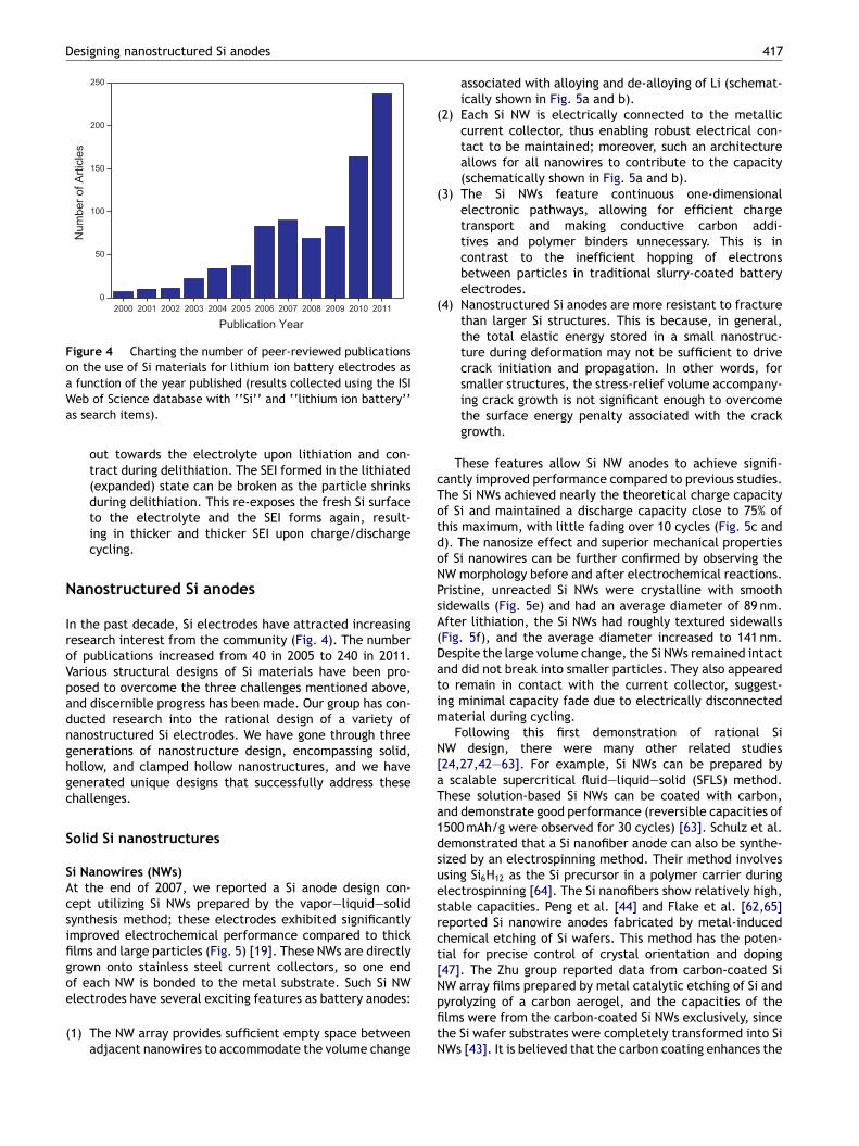
Figure 4 Charting the number of peer-reviewed publicationson the use of Si materials for lithium ion battery electrodes asa function of the year published (results collected using the ISI
(
(
(
cTotdoNPsA(Datim
N[aTa1dsuesrct[N
Web of Science database with ‘‘Si’’ and ‘‘lithium ion battery’’as search items).
out towards the electrolyte upon lithiation and con-tract during delithiation. The SEI formed in the lithiated(expanded) state can be broken as the particle shrinksduring delithiation. This re-exposes the fresh Si surfaceto the electrolyte and the SEI forms again, result-ing in thicker and thicker SEI upon charge/dischargecycling.
Nanostructured Si anodes
In the past decade, Si electrodes have attracted increasingresearch interest from the community (Fig. 4). The numberof publications increased from 40 in 2005 to 240 in 2011.Various structural designs of Si materials have been pro-posed to overcome the three challenges mentioned above,and discernible progress has been made. Our group has con-ducted research into the rational design of a variety ofnanostructured Si electrodes. We have gone through threegenerations of nanostructure design, encompassing solid,hollow, and clamped hollow nanostructures, and we havegenerated unique designs that successfully address thesechallenges.
Solid Si nanostructures
Si Nanowires (NWs)At the end of 2007, we reported a Si anode design con-cept utilizing Si NWs prepared by the vapor—liquid—solidsynthesis method; these electrodes exhibited significantlyimproved electrochemical performance compared to thickfilms and large particles (Fig. 5) [19]. These NWs are directlygrown onto stainless steel current collectors, so one endof each NW is bonded to the metal substrate. Such Si NWelectrodes have several exciting features as battery anodes:
(1) The NW array provides sufficient empty space betweenadjacent nanowires to accommodate the volume change
pfitN
417
associated with alloying and de-alloying of Li (schemat-ically shown in Fig. 5a and b).
2) Each Si NW is electrically connected to the metalliccurrent collector, thus enabling robust electrical con-tact to be maintained; moreover, such an architectureallows for all nanowires to contribute to the capacity(schematically shown in Fig. 5a and b).
3) The Si NWs feature continuous one-dimensionalelectronic pathways, allowing for efficient chargetransport and making conductive carbon addi-tives and polymer binders unnecessary. This is incontrast to the inefficient hopping of electronsbetween particles in traditional slurry-coated batteryelectrodes.
4) Nanostructured Si anodes are more resistant to fracturethan larger Si structures. This is because, in general,the total elastic energy stored in a small nanostruc-ture during deformation may not be sufficient to drivecrack initiation and propagation. In other words, forsmaller structures, the stress-relief volume accompany-ing crack growth is not significant enough to overcomethe surface energy penalty associated with the crackgrowth.
These features allow Si NW anodes to achieve signifi-antly improved performance compared to previous studies.he Si NWs achieved nearly the theoretical charge capacityf Si and maintained a discharge capacity close to 75% ofhis maximum, with little fading over 10 cycles (Fig. 5c and). The nanosize effect and superior mechanical propertiesf Si nanowires can be further confirmed by observing theW morphology before and after electrochemical reactions.ristine, unreacted Si NWs were crystalline with smoothidewalls (Fig. 5e) and had an average diameter of 89 nm.fter lithiation, the Si NWs had roughly textured sidewallsFig. 5f), and the average diameter increased to 141 nm.espite the large volume change, the Si NWs remained intactnd did not break into smaller particles. They also appearedo remain in contact with the current collector, suggest-ng minimal capacity fade due to electrically disconnectedaterial during cycling.Following this first demonstration of rational Si
W design, there were many other related studies24,27,42—63]. For example, Si NWs can be prepared by
scalable supercritical fluid—liquid—solid (SFLS) method.hese solution-based Si NWs can be coated with carbon,nd demonstrate good performance (reversible capacities of500 mAh/g were observed for 30 cycles) [63]. Schulz et al.emonstrated that a Si nanofiber anode can also be synthe-ized by an electrospinning method. Their method involvessing Si6H12 as the Si precursor in a polymer carrier duringlectrospinning [64]. The Si nanofibers show relatively high,table capacities. Peng et al. [44] and Flake et al. [62,65]eported Si nanowire anodes fabricated by metal-inducedhemical etching of Si wafers. This method has the poten-ial for precise control of crystal orientation and doping47]. The Zhu group reported data from carbon-coated SiW array films prepared by metal catalytic etching of Si and
yrolyzing of a carbon aerogel, and the capacities of thelms were from the carbon-coated Si NWs exclusively, sincehe Si wafer substrates were completely transformed into SiWs [43]. It is believed that the carbon coating enhances the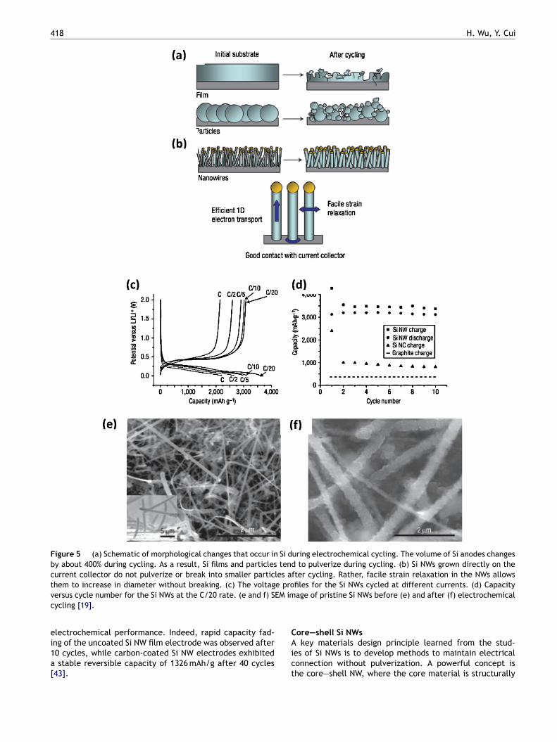
418 H. Wu, Y. Cui
Figure 5 (a) Schematic of morphological changes that occur in Si during electrochemical cycling. The volume of Si anodes changesby about 400% during cycling. As a result, Si films and particles tend to pulverize during cycling. (b) Si NWs grown directly on thecurrent collector do not pulverize or break into smaller particles after cycling. Rather, facile strain relaxation in the NWs allowsthem to increase in diameter without breaking. (c) The voltage profiles for the Si NWs cycled at different currents. (d) Capacityv EM imc
ei1a[
CA
ersus cycle number for the Si NWs at the C/20 rate. (e and f) Sycling [19].
lectrochemical performance. Indeed, rapid capacity fad-ng of the uncoated Si NW film electrode was observed after
0 cycles, while carbon-coated Si NW electrodes exhibitedstable reversible capacity of 1326 mAh/g after 40 cycles43].
ict
age of pristine Si NWs before (e) and after (f) electrochemical
ore—shell Si NWskey materials design principle learned from the stud-
es of Si NWs is to develop methods to maintain electricalonnection without pulverization. A powerful concept ishe core—shell NW, where the core material is structurally
Designing nanostructured Si anodes 419
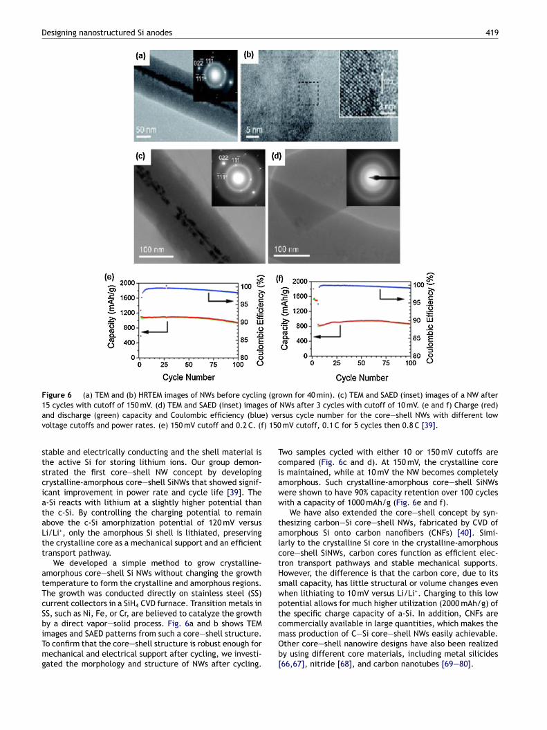
Figure 6 (a) TEM and (b) HRTEM images of NWs before cycling (grown for 40 min). (c) TEM and SAED (inset) images of a NW after15 cycles with cutoff of 150 mV. (d) TEM and SAED (inset) images of NWs after 3 cycles with cutoff of 10 mV. (e and f) Charge (red)
) ve) 150
Tciaww
talctHswptc
and discharge (green) capacity and Coulombic efficiency (bluevoltage cutoffs and power rates. (e) 150 mV cutoff and 0.2 C. (f
stable and electrically conducting and the shell material isthe active Si for storing lithium ions. Our group demon-strated the first core—shell NW concept by developingcrystalline-amorphous core—shell SiNWs that showed signif-icant improvement in power rate and cycle life [39]. Thea-Si reacts with lithium at a slightly higher potential thanthe c-Si. By controlling the charging potential to remainabove the c-Si amorphization potential of 120 mV versusLi/Li+, only the amorphous Si shell is lithiated, preservingthe crystalline core as a mechanical support and an efficienttransport pathway.
We developed a simple method to grow crystalline-amorphous core—shell Si NWs without changing the growthtemperature to form the crystalline and amorphous regions.The growth was conducted directly on stainless steel (SS)current collectors in a SiH4 CVD furnace. Transition metals inSS, such as Ni, Fe, or Cr, are believed to catalyze the growthby a direct vapor—solid process. Fig. 6a and b shows TEM
images and SAED patterns from such a core—shell structure.To confirm that the core—shell structure is robust enough formechanical and electrical support after cycling, we investi-gated the morphology and structure of NWs after cycling.mOb[
rsus cycle number for the core—shell NWs with different lowmV cutoff, 0.1 C for 5 cycles then 0.8 C [39].
wo samples cycled with either 10 or 150 mV cutoffs areompared (Fig. 6c and d). At 150 mV, the crystalline cores maintained, while at 10 mV the NW becomes completelymorphous. Such crystalline-amorphous core—shell SiNWsere shown to have 90% capacity retention over 100 cyclesith a capacity of 1000 mAh/g (Fig. 6e and f).
We have also extended the core—shell concept by syn-hesizing carbon—Si core—shell NWs, fabricated by CVD ofmorphous Si onto carbon nanofibers (CNFs) [40]. Simi-arly to the crystalline Si core in the crystalline-amorphousore—shell SiNWs, carbon cores function as efficient elec-ron transport pathways and stable mechanical supports.owever, the difference is that the carbon core, due to itsmall capacity, has little structural or volume changes evenhen lithiating to 10 mV versus Li/Li+. Charging to this lowotential allows for much higher utilization (2000 mAh/g) ofhe specific charge capacity of a-Si. In addition, CNFs areommercially available in large quantities, which makes the
ass production of C—Si core—shell NWs easily achievable.ther core—shell nanowire designs have also been realizedy using different core materials, including metal silicides66,67], nitride [68], and carbon nanotubes [69—80].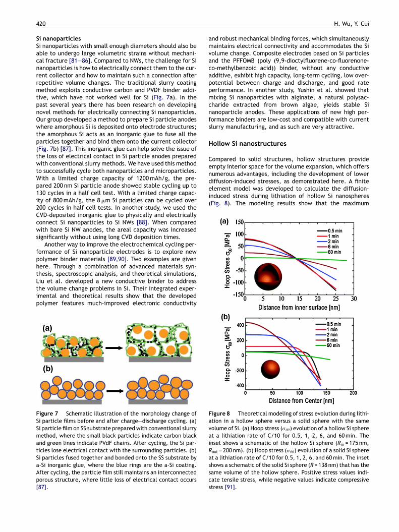
420 H. Wu, Y. Cui
Si nanoparticlesSi nanoparticles with small enough diameters should also beable to undergo large volumetric strains without mechani-cal fracture [81—86]. Compared to NWs, the challenge for Sinanoparticles is how to electrically connect them to the cur-rent collector and how to maintain such a connection afterrepetitive volume changes. The traditional slurry coatingmethod exploits conductive carbon and PVDF binder addi-tive, which have not worked well for Si (Fig. 7a). In thepast several years there has been research on developingnovel methods for electrically connecting Si nanoparticles.Our group developed a method to prepare Si particle anodeswhere amorphous Si is deposited onto electrode structures;the amorphous Si acts as an inorganic glue to fuse all theparticles together and bind them onto the current collector(Fig. 7b) [87]. This inorganic glue can help solve the issue ofthe loss of electrical contact in Si particle anodes preparedwith conventional slurry methods. We have used this methodto successfully cycle both nanoparticles and microparticles.With a limited charge capacity of 1200 mAh/g, the pre-pared 200 nm Si particle anode showed stable cycling up to130 cycles in a half cell test. With a limited charge capac-ity of 800 mAh/g, the 8 �m Si particles can be cycled over200 cycles in half cell tests. In another study, we used theCVD-deposited inorganic glue to physically and electricallyconnect Si nanoparticles to Si NWs [88]. When comparedwith bare Si NW anodes, the areal capacity was increasedsignificantly without using long CVD deposition times.
Another way to improve the electrochemical cycling per-formance of Si nanoparticle electrodes is to explore newpolymer binder materials [89,90]. Two examples are givenhere. Through a combination of advanced materials syn-thesis, spectroscopic analysis, and theoretical simulations,Liu et al. developed a new conductive binder to addressthe volume change problems in Si. Their integrated exper-imental and theoretical results show that the developedpolymer features much-improved electronic conductivity
Figure 7 Schematic illustration of the morphology change ofSi particle films before and after charge—discharge cycling. (a)Si particle film on SS substrate prepared with conventional slurrymethod, where the small black particles indicate carbon blackand green lines indicate PVdF chains. After cycling, the Si par-ticles lose electrical contact with the surrounding particles. (b)Si particles fused together and bonded onto the SS substrate bya-Si inorganic glue, where the blue rings are the a-Si coating.After cycling, the particle film still maintains an interconnectedporous structure, where little loss of electrical contact occurs[87].
and robust mechanical binding forces, which simultaneouslymaintains electrical connectivity and accommodates the Sivolume change. Composite electrodes based on Si particlesand the PFFOMB (poly (9,9-dioctylfluorene-co-fluorenone-co-methylbenzoic acid)) binder, without any conductiveadditive, exhibit high capacity, long-term cycling, low over-potential between charge and discharge, and good rateperformance. In another study, Yushin et al. showed thatmixing Si nanoparticles with alginate, a natural polysac-charide extracted from brown algae, yields stable Sinanoparticle anodes. These applications of new high per-formance binders are low-cost and compatible with currentslurry manufacturing, and as such are very attractive.
Hollow Si nanostructures
Compared to solid structures, hollow structures provideempty interior space for the volume expansion, which offersnumerous advantages, including the development of lowerdiffusion-induced stresses, as demonstrated here. A finiteelement model was developed to calculate the diffusion-induced stress during lithiation of hollow Si nanospheres(Fig. 8). The modeling results show that the maximum
Figure 8 Theoretical modeling of stress evolution during lithi-ation in a hollow sphere versus a solid sphere with the samevolume of Si. (a) Hoop stress (���) evolution of a hollow Si sphereat a lithiation rate of C/10 for 0.5, 1, 2, 6, and 60 min. Theinset shows a schematic of the hollow Si sphere (Rin = 175 nm,Rout = 200 nm). (b) Hoop stress (���) evolution of a solid Si sphereat a lithiation rate of C/10 for 0.5, 1, 2, 6, and 60 min. The insetshows a schematic of the solid Si sphere (R = 138 nm) that has thesame volume of the hollow sphere. Positive stress values indi-cate tensile stress, while negative values indicate compressivestress [91].
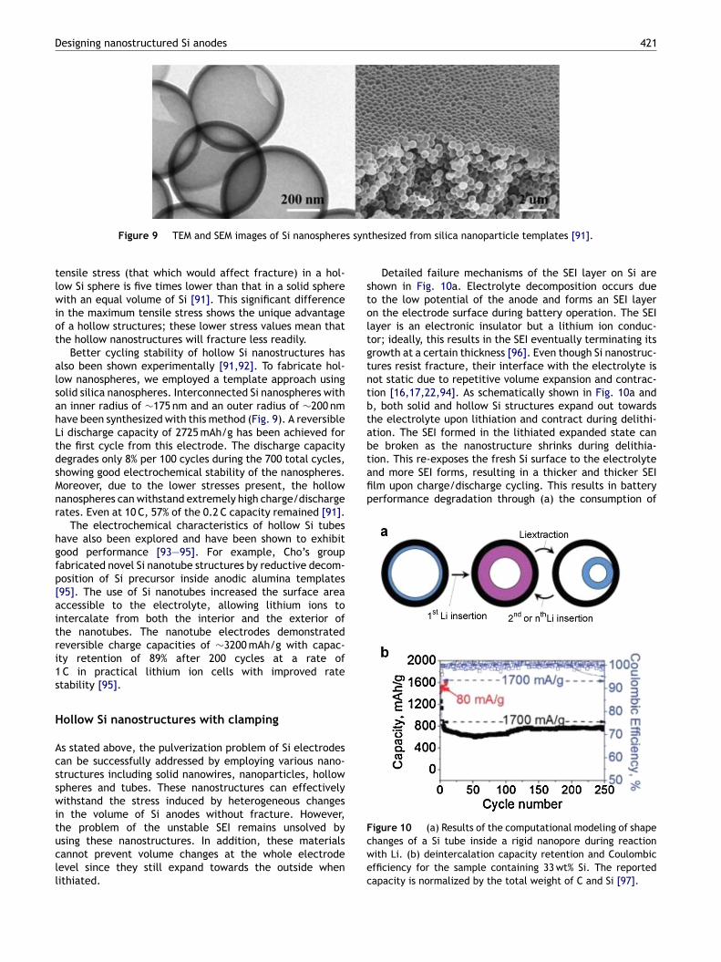
Designing nanostructured Si anodes 421
s synthesized from silica nanoparticle templates [91].
Detailed failure mechanisms of the SEI layer on Si areshown in Fig. 10a. Electrolyte decomposition occurs dueto the low potential of the anode and forms an SEI layeron the electrode surface during battery operation. The SEIlayer is an electronic insulator but a lithium ion conduc-tor; ideally, this results in the SEI eventually terminating itsgrowth at a certain thickness [96]. Even though Si nanostruc-tures resist fracture, their interface with the electrolyte isnot static due to repetitive volume expansion and contrac-tion [16,17,22,94]. As schematically shown in Fig. 10a andb, both solid and hollow Si structures expand out towardsthe electrolyte upon lithiation and contract during delithi-ation. The SEI formed in the lithiated expanded state canbe broken as the nanostructure shrinks during delithia-tion. This re-exposes the fresh Si surface to the electrolyteand more SEI forms, resulting in a thicker and thicker SEIfilm upon charge/discharge cycling. This results in batteryperformance degradation through (a) the consumption of
Figure 10 (a) Results of the computational modeling of shape
Figure 9 TEM and SEM images of Si nanosphere
tensile stress (that which would affect fracture) in a hol-low Si sphere is five times lower than that in a solid spherewith an equal volume of Si [91]. This significant differencein the maximum tensile stress shows the unique advantageof a hollow structures; these lower stress values mean thatthe hollow nanostructures will fracture less readily.
Better cycling stability of hollow Si nanostructures hasalso been shown experimentally [91,92]. To fabricate hol-low nanospheres, we employed a template approach usingsolid silica nanospheres. Interconnected Si nanospheres withan inner radius of ∼175 nm and an outer radius of ∼200 nmhave been synthesized with this method (Fig. 9). A reversibleLi discharge capacity of 2725 mAh/g has been achieved forthe first cycle from this electrode. The discharge capacitydegrades only 8% per 100 cycles during the 700 total cycles,showing good electrochemical stability of the nanospheres.Moreover, due to the lower stresses present, the hollownanospheres can withstand extremely high charge/dischargerates. Even at 10 C, 57% of the 0.2 C capacity remained [91].
The electrochemical characteristics of hollow Si tubeshave also been explored and have been shown to exhibitgood performance [93—95]. For example, Cho’s groupfabricated novel Si nanotube structures by reductive decom-position of Si precursor inside anodic alumina templates[95]. The use of Si nanotubes increased the surface areaaccessible to the electrolyte, allowing lithium ions tointercalate from both the interior and the exterior ofthe nanotubes. The nanotube electrodes demonstratedreversible charge capacities of ∼3200 mAh/g with capac-ity retention of 89% after 200 cycles at a rate of1 C in practical lithium ion cells with improved ratestability [95].
Hollow Si nanostructures with clamping
As stated above, the pulverization problem of Si electrodescan be successfully addressed by employing various nano-structures including solid nanowires, nanoparticles, hollowspheres and tubes. These nanostructures can effectivelywithstand the stress induced by heterogeneous changesin the volume of Si anodes without fracture. However,the problem of the unstable SEI remains unsolved by
using these nanostructures. In addition, these materialscannot prevent volume changes at the whole electrodelevel since they still expand towards the outside whenlithiated.changes of a Si tube inside a rigid nanopore during reactionwith Li. (b) deintercalation capacity retention and Coulombicefficiency for the sample containing 33 wt% Si. The reportedcapacity is normalized by the total weight of C and Si [97].
422 H. Wu, Y. Cui
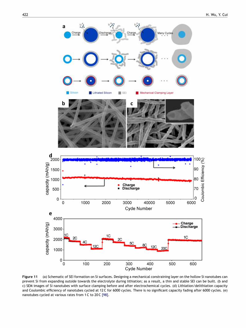
Figure 11 (a) Schematic of SEI formation on Si surfaces. Designing a mechanical constraining layer on the hollow Si nanotubes canprevent Si from expanding outside towards the electrolyte during lithiation; as a result, a thin and stable SEI can be built. (b andc) SEM images of Si nanotubes with surface clamping before and after electrochemical cycles. (d) Lithiation/delithiation capacityand Coulombic efficiency of nanotubes cycled at 12 C for 6000 cycles. There is no significant capacity fading after 6000 cycles. (e)nanotubes cycled at various rates from 1 C to 20 C [98].
423
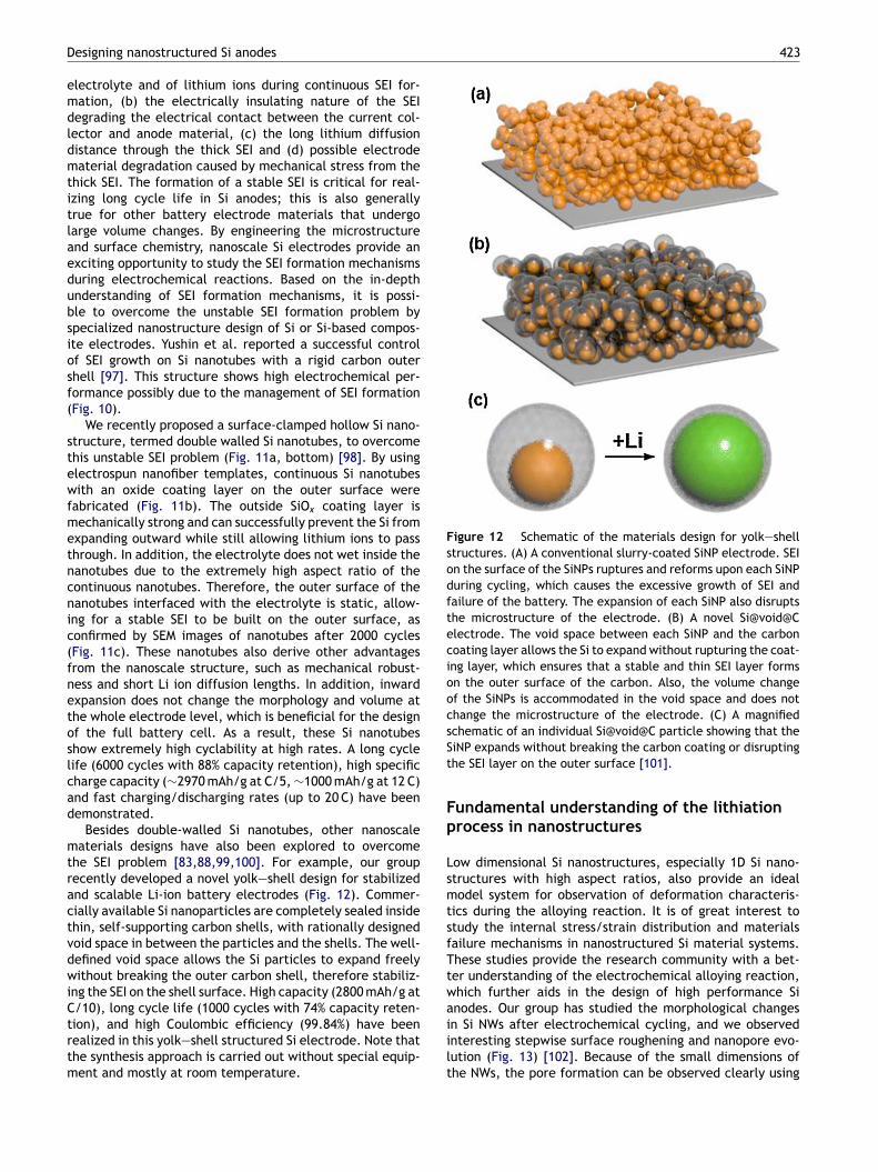
Figure 12 Schematic of the materials design for yolk—shellstructures. (A) A conventional slurry-coated SiNP electrode. SEIon the surface of the SiNPs ruptures and reforms upon each SiNPduring cycling, which causes the excessive growth of SEI andfailure of the battery. The expansion of each SiNP also disruptsthe microstructure of the electrode. (B) A novel Si@void@Celectrode. The void space between each SiNP and the carboncoating layer allows the Si to expand without rupturing the coat-ing layer, which ensures that a stable and thin SEI layer formson the outer surface of the carbon. Also, the volume changeof the SiNPs is accommodated in the void space and does notchange the microstructure of the electrode. (C) A magnifiedschematic of an individual Si@void@C particle showing that theSt
Fp
LsmtsfTtwa
Designing nanostructured Si anodes
electrolyte and of lithium ions during continuous SEI for-mation, (b) the electrically insulating nature of the SEIdegrading the electrical contact between the current col-lector and anode material, (c) the long lithium diffusiondistance through the thick SEI and (d) possible electrodematerial degradation caused by mechanical stress from thethick SEI. The formation of a stable SEI is critical for real-izing long cycle life in Si anodes; this is also generallytrue for other battery electrode materials that undergolarge volume changes. By engineering the microstructureand surface chemistry, nanoscale Si electrodes provide anexciting opportunity to study the SEI formation mechanismsduring electrochemical reactions. Based on the in-depthunderstanding of SEI formation mechanisms, it is possi-ble to overcome the unstable SEI formation problem byspecialized nanostructure design of Si or Si-based compos-ite electrodes. Yushin et al. reported a successful controlof SEI growth on Si nanotubes with a rigid carbon outershell [97]. This structure shows high electrochemical per-formance possibly due to the management of SEI formation(Fig. 10).
We recently proposed a surface-clamped hollow Si nano-structure, termed double walled Si nanotubes, to overcomethis unstable SEI problem (Fig. 11a, bottom) [98]. By usingelectrospun nanofiber templates, continuous Si nanotubeswith an oxide coating layer on the outer surface werefabricated (Fig. 11b). The outside SiOx coating layer ismechanically strong and can successfully prevent the Si fromexpanding outward while still allowing lithium ions to passthrough. In addition, the electrolyte does not wet inside thenanotubes due to the extremely high aspect ratio of thecontinuous nanotubes. Therefore, the outer surface of thenanotubes interfaced with the electrolyte is static, allow-ing for a stable SEI to be built on the outer surface, asconfirmed by SEM images of nanotubes after 2000 cycles(Fig. 11c). These nanotubes also derive other advantagesfrom the nanoscale structure, such as mechanical robust-ness and short Li ion diffusion lengths. In addition, inwardexpansion does not change the morphology and volume atthe whole electrode level, which is beneficial for the designof the full battery cell. As a result, these Si nanotubesshow extremely high cyclability at high rates. A long cyclelife (6000 cycles with 88% capacity retention), high specificcharge capacity (∼2970 mAh/g at C/5, ∼1000 mAh/g at 12 C)and fast charging/discharging rates (up to 20 C) have beendemonstrated.
Besides double-walled Si nanotubes, other nanoscalematerials designs have also been explored to overcomethe SEI problem [83,88,99,100]. For example, our grouprecently developed a novel yolk—shell design for stabilizedand scalable Li-ion battery electrodes (Fig. 12). Commer-cially available Si nanoparticles are completely sealed insidethin, self-supporting carbon shells, with rationally designedvoid space in between the particles and the shells. The well-defined void space allows the Si particles to expand freelywithout breaking the outer carbon shell, therefore stabiliz-ing the SEI on the shell surface. High capacity (2800 mAh/g atC/10), long cycle life (1000 cycles with 74% capacity reten-
tion), and high Coulombic efficiency (99.84%) have beenrealized in this yolk—shell structured Si electrode. Note thatthe synthesis approach is carried out without special equip-ment and mostly at room temperature.iilt
iNP expands without breaking the carbon coating or disruptinghe SEI layer on the outer surface [101].
undamental understanding of the lithiationrocess in nanostructures
ow dimensional Si nanostructures, especially 1D Si nano-tructures with high aspect ratios, also provide an idealodel system for observation of deformation characteris-
ics during the alloying reaction. It is of great interest totudy the internal stress/strain distribution and materialsailure mechanisms in nanostructured Si material systems.hese studies provide the research community with a bet-er understanding of the electrochemical alloying reaction,hich further aids in the design of high performance Sinodes. Our group has studied the morphological changes
n Si NWs after electrochemical cycling, and we observednteresting stepwise surface roughening and nanopore evo-ution (Fig. 13) [102]. Because of the small dimensions ofhe NWs, the pore formation can be observed clearly using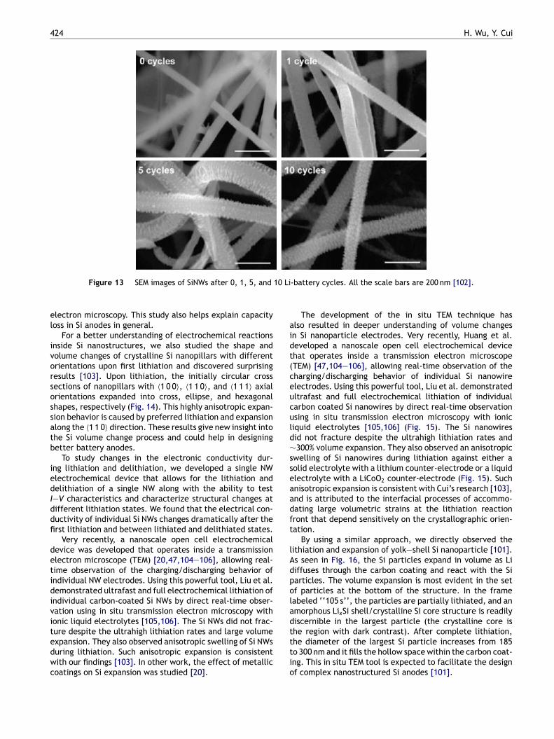
424 H. Wu, Y. Cui
10 Li
el
ivorsossatb
iedIddfi
detidivitedwc
aidt(ceuculd∼sseaadft
lAdpoladt
Figure 13 SEM images of SiNWs after 0, 1, 5, and
lectron microscopy. This study also helps explain capacityoss in Si anodes in general.
For a better understanding of electrochemical reactionsnside Si nanostructures, we also studied the shape andolume changes of crystalline Si nanopillars with differentrientations upon first lithiation and discovered surprisingesults [103]. Upon lithiation, the initially circular crossections of nanopillars with 〈1 0 0〉, 〈1 1 0〉, and 〈1 1 1〉 axialrientations expanded into cross, ellipse, and hexagonalhapes, respectively (Fig. 14). This highly anisotropic expan-ion behavior is caused by preferred lithiation and expansionlong the 〈1 1 0〉 direction. These results give new insight intohe Si volume change process and could help in designingetter battery anodes.
To study changes in the electronic conductivity dur-ng lithiation and delithiation, we developed a single NWlectrochemical device that allows for the lithiation andelithiation of a single NW along with the ability to test—V characteristics and characterize structural changes atifferent lithiation states. We found that the electrical con-uctivity of individual Si NWs changes dramatically after therst lithiation and between lithiated and delithiated states.
Very recently, a nanoscale open cell electrochemicalevice was developed that operates inside a transmissionlectron microscope (TEM) [20,47,104—106], allowing real-ime observation of the charging/discharging behavior ofndividual NW electrodes. Using this powerful tool, Liu et al.emonstrated ultrafast and full electrochemical lithiation ofndividual carbon-coated Si NWs by direct real-time obser-ation using in situ transmission electron microscopy withonic liquid electrolytes [105,106]. The Si NWs did not frac-ure despite the ultrahigh lithiation rates and large volume
xpansion. They also observed anisotropic swelling of Si NWsuring lithiation. Such anisotropic expansion is consistentith our findings [103]. In other work, the effect of metallicoatings on Si expansion was studied [20].ttio
-battery cycles. All the scale bars are 200 nm [102].
The development of the in situ TEM technique haslso resulted in deeper understanding of volume changesn Si nanoparticle electrodes. Very recently, Huang et al.eveloped a nanoscale open cell electrochemical devicehat operates inside a transmission electron microscopeTEM) [47,104—106], allowing real-time observation of theharging/discharging behavior of individual Si nanowirelectrodes. Using this powerful tool, Liu et al. demonstratedltrafast and full electrochemical lithiation of individualarbon coated Si nanowires by direct real-time observationsing in situ transmission electron microscopy with ioniciquid electrolytes [105,106] (Fig. 15). The Si nanowiresid not fracture despite the ultrahigh lithiation rates and300% volume expansion. They also observed an anisotropic
welling of Si nanowires during lithiation against either aolid electrolyte with a lithium counter-electrode or a liquidlectrolyte with a LiCoO2 counter-electrode (Fig. 15). Suchnisotropic expansion is consistent with Cui’s research [103],nd is attributed to the interfacial processes of accommo-ating large volumetric strains at the lithiation reactionront that depend sensitively on the crystallographic orien-ation.
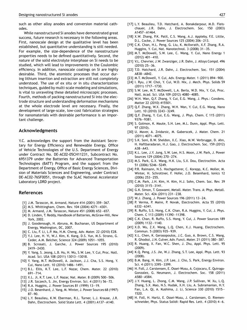
By using a similar approach, we directly observed theithiation and expansion of yolk—shell Si nanoparticle [101].s seen in Fig. 16, the Si particles expand in volume as Liiffuses through the carbon coating and react with the Siarticles. The volume expansion is most evident in the setf particles at the bottom of the structure. In the frameabeled ‘‘105 s’’, the particles are partially lithiated, and anmorphous LixSi shell/crystalline Si core structure is readilyiscernible in the largest particle (the crystalline core ishe region with dark contrast). After complete lithiation,
he diameter of the largest Si particle increases from 185o 300 nm and it fills the hollow space within the carbon coat-ng. This in situ TEM tool is expected to facilitate the designf complex nanostructured Si anodes [101].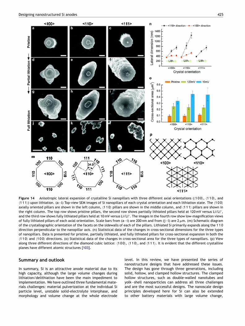
Designing nanostructured Si anodes 425
Figure 14 Anisotropic lateral expansion of crystalline Si nanopillars with three different axial orientations (〈1 0 0〉, 〈1 1 0〉, and〈1 1 1〉) upon lithiation. (a—l) Top-view SEM images of Si nanopillars of each crystal orientation and each lithiation state. The 〈1 0 0〉axially oriented pillars are shown in the left column, 〈1 1 0〉 pillars are shown in the middle column, and 〈1 1 1〉 pillars are shown inthe right column. The top row shows pristine pillars, the second row shows partially lithiated pillars held at 120 mV versus Li/Li+,and the third row shows fully lithiated pillars held at 10 mV versus Li/Li+. The images in the fourth row show low-magnification viewsof fully lithiated pillars of each axial orientation. Scale bars from (a—i) are 200 nm and from (j—l) are 2 �m. (m) Schematic diagramof the crystallographic orientation of the facets on the sidewalls of each of the pillars. Lithiated Si primarily expands along the 1 1 0direction perpendicular to the nanopillar axis. (n) Statistical data of the changes in cross-sectional dimensions for the three typesof nanopillars. Data is presented for pristine, partially lithiated, and fully lithiated pillars for cross-sectional expansion in both the〈1 1 0〉 and 〈1 0 0〉 directions. (o) Statistical data of the changes in cross-sectional area for the three types of nanopillars. (p) View
1 0 0〉
lnTshy
along three different directions of the diamond cubic lattice: 〈planes have different atomic structures [103].
Summary and outlook
In summary, Si is an attractive anode material due to itshigh capacity, although the large volume changes duringlithiation/delithiation have been the main impediment toimplementation. We have outlined three fundamental mate-
rials challenges: material pulverization at the individual Siparticle level, unstable solid-electrolyte interphase, andmorphology and volume change at the whole electrodeapt
, 〈1 1 0〉, and 〈1 1 1〉. It is evident that the different crystalline
evel. In this review, we have presented the series ofanostructure designs that have addressed these issues.he design has gone through three generations, includingolid, hollow, and clamped hollow structures. The clampedollow structures, such as double-walled nanotubes andolk—shell nanoparticles can address all three challenges
nd are the most successful designs. The nanoscale designrinciples developed here for Si can also be extendedo other battery materials with large volume change,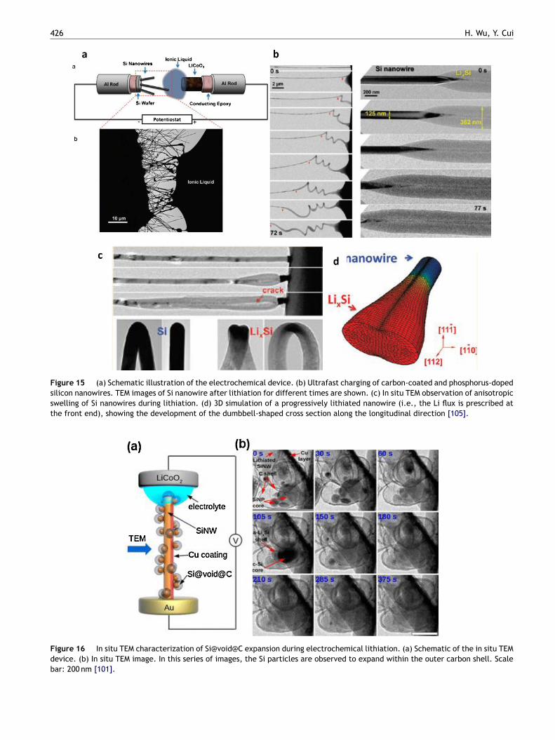
426 H. Wu, Y. Cui
Figure 15 (a) Schematic illustration of the electrochemical device. (b) Ultrafast charging of carbon-coated and phosphorus-dopedsilicon nanowires. TEM images of Si nanowire after lithiation for different times are shown. (c) In situ TEM observation of anisotropicswelling of Si nanowires during lithiation. (d) 3D simulation of a progressively lithiated nanowire (i.e., the Li flux is prescribed atthe front end), showing the development of the dumbbell-shaped cross section along the longitudinal direction [105].
Figure 16 In situ TEM characterization of Si@void@C expansion during electrochemical lithiation. (a) Schematic of the in situ TEMdevice. (b) In situ TEM image. In this series of images, the Si particles are observed to expand within the outer carbon shell. Scalebar: 200 nm [101].
Designing nanostructured Si anodes
such as other alloy anodes and conversion material cath-odes.
While nanostructured Si anodes have demonstrated greatsuccess, future research is necessary in the following areas.First, nanoscale design at the qualitative level has beenestablished, but quantitative understanding is still needed.For example, the size-dependence of the nanostructureproperties needs to be defined quantitatively. Second, thenature of the solid electrolyte interphase on Si needs to bestudied, which will lead to improvements in the Coulombicefficiency. In addition, nanoscale coatings on Si are highlydesirable. Third, the atomistic processes that occur dur-ing lithium insertion and extraction are still not completelyunderstood. The use of ex situ or in situ characterizationtechniques, guided by multi-scale modeling and simulations,is vital to unraveling these detailed microscopic processes.Fourth, methods of packing nanostructured Si into the elec-trode structure and understanding deformation mechanismsat the whole electrode level are necessary. Finally, thedevelopment of large-scale, low-cost fabrication strategiesfor nanomaterials with desirable performance is an impor-tant challenge.
Acknowledgments
Y.C. acknowledges the support from the Assistant Secre-tary for Energy Efficiency and Renewable Energy, Officeof Vehicle Technologies of the U.S. Department of Energyunder Contract No. DE-AC02-05CH11231, Subcontract No.6951379 under the Batteries for Advanced TransportationTechnologies (BATT) Program, and the support from theDepartment of Energy, Office of Basic Energy Sciences, Divi-sion of Materials Sciences and Engineering, under ContractDE-AC02-76SF0051, through the SLAC National AcceleratorLaboratory LDRD project.
References
[1] J.M. Tarascon, M. Armand, Nature 414 (2001) 359—367.[2] M.S. Whittingham, Chem. Rev. 104 (2004) 4271—4301.[3] M. Armand, J.M. Tarascon, Nature 451 (2008) 652—657.[4] D. Linden, T. Reddy, Handbook of Batteries, McGraw-Hill, New
York, 2002.[5] J. Goodenough, H. Abruna, M. Buchanan, US Department of
Energy, Washington, DC, 2007.[6] C. Liu, F. Li, L.P. Ma, H.M. Cheng, Adv. Mater. 22 (2010) E28.[7] Y.J. Lee, H. Yi, W.J. Kim, K. Kang, D.S. Yun, M.S. Strano, G.
Ceder, A.M. Belcher, Science 324 (2009) 1051—1055.[8] B. Scrosati, J. Garche, J. Power Sources 195 (2010)
2419—2430.[9] Y. Yang, S. Jeong, L.B. Hu, H. Wu, S.W. Lee, Y. Cui, Proc. Natl.
Acad. Sci. USA 108 (2011) 13013—13018.[10] Y. Yang, M.T. McDowell, A. Jackson, J.J. Cha, S.S. Hong, Y.
Cui, Nano Lett. 10 (2010) 1486—1491.[11] B.L. Ellis, K.T. Lee, L.F. Nazar, Chem. Mater. 22 (2010)
691—714.[12] X.L. Ji, K.T. Lee, L.F. Nazar, Nat. Mater. 8 (2009) 500—506.[13] J.R. Szczech, S. Jin, Energy Environ. Sci. 4 (2011) 56—72.[14] R.A. Huggins, J. Power Sources 81 (1999) 13—19.
[15] J.O. Besenhard, J. Yang, M. Winter, J. Power Sources 68 (1997)87—90.[16] L.Y. Beaulieu, K.W. Eberman, R.L. Turner, L.J. Krause, J.R.
Dahn, Electrochem. Solid State Lett. 4 (2001) A137—A140.
427
[17] L.Y. Beaulieu, T.D. Hatchard, A. Bonakdarpour, M.D. Fleis-chauer, J.R. Dahn, J. Electrochem. Soc. 150 (2003)A1457—A1464.
[18] X.W. Zhang, P.K. Patil, C.S. Wang, A.J. Appleby, F.E. Little,D.L. Cocke, J. Power Sources 125 (2004) 206—213.
[19] C.K. Chan, H.L. Peng, G. Liu, K. McIlwrath, X.F. Zhang, R.A.Huggins, Y. Cui, Nat. Nanotechnol. 3 (2008) 31—35.
[20] M.T. McDowell, S.W. Lee, C. Wang, Y. Cui, Nano Energy 1(2012) 401—410.
[21] V.L. Chevrier, J.W. Zwanziger, J.R. Dahn, J. Alloys Compd. 496(2010) 25—36.
[22] T.D. Hatchard, J.R. Dahn, J. Electrochem. Soc. 151 (2004)A838—A842.
[23] M.T. McDowell, Y. Cui, Adv. Energy Mater. 1 (2011) 894—900.[24] I. Ryu, J.W. Choi, Y. Cui, W.D. Nix, J. Mech. Phys. Solids 59
(2011) 1717—1730.[25] S.W. Lee, M.T. McDowell, L.A. Berla, W.D. Nix, Y. Cui, Proc.
Natl. Acad. Sci. USA 109 (2012) 4080—4085.[26] W.H. Wan, Q.F. Zhang, Y. Cui, E.G. Wang, J. Phys.: Condens.
Matter 22 (2010) 415501.[27] Q.F. Zhang, W.X. Zhang, W.H. Wan, Y. Cui, E.G. Wang, Nano
Lett. 10 (2010) 3243—3249.[28] Q.F. Zhang, Y. Cui, E.G. Wang, J. Phys. Chem. C 115 (2011)
9376—9381.[29] S. Golmon, K. Maute, S.H. Lee, M.L. Dunn, Appl. Phys. Lett.
97 (2010).[30] U. Maver, A. Znidarsic, M. Gaberscek, J. Mater. Chem. 21
(2011) 4071—4075.[31] S.K. Soni, B.W. Sheldon, X.C. Xiao, M.W. Verbrugge, D. Ahn,
H. Haftbaradaran, H.J. Gao, J. Electrochem. Soc. 159 (2012)A38—A43.
[32] K.L. Lee, J.Y. Jung, S.W. Lee, H.S. Moon, J.W. Park, J. PowerSources 129 (2004) 270—274.
[33] M.S. Park, G.X. Wang, H.K. Liu, S.X. Dou, Electrochim. Acta51 (2006) 5246—5249.
[34] P.R. Raimann, N.S. Hochgatterer, C. Korepp, K.C. Moller, M.Winter, H. Schrottner, F. Hofer, J.O. Besenhard, Ionics 12(2006) 253—255.
[35] C.M. Park, J.H. Kim, H. Kim, H.J. Sohn, Chem. Soc. Rev. 39(2010) 3115—3141.
[36] G.K. Simon, T. Goswami, Metall. Mater. Trans. A: Phys. Metall.Mater. Sci. 42A (2011) 231—238.
[37] W.J. Zhang, J. Power Sources 196 (2011) 13—24.[38] P. Verma, P. Maire, P. Novak, Electrochim. Acta 55 (2010)
6332—6341.[39] R. Ruffo, S.S. Hong, C.K. Chan, R.A. Huggins, Y. Cui, J. Phys.
Chem. C 113 (2009) 11390—11398.[40] C.K. Chan, R. Ruffo, S.S. Hong, Y. Cui, J. Power Sources 189
(2009) 1132—1140.[41] X.D. Wu, Z.X. Wang, L.Q. Chen, X.J. Huang, Electrochem.
Commun. 5 (2003) 935—939.[42] X.L. Chen, K. Gerasopoulos, J.C. Guo, A. Brown, C.S. Wang,
R. Ghodssi, J.N. Culver, Adv. Funct. Mater. 21 (2011) 380—387.[43] R. Huang, X. Fan, W.C. Shen, J. Zhu, Appl. Phys. Lett. 95
(2009).[44] K.Q. Peng, J.S. Jie, W.J. Zhang, S.T. Lee, Appl. Phys. Lett. 93
(2008).[45] B.M. Bang, H. Kim, J.P. Lee, J. Cho, S. Park, Energy Environ.
Sci. 4 (2011) 3395—3399.[46] H. Foll, J. Carstensen, E. Ossei-Wusu, A. Cojocaru, E. Quiroga-
Gonzalez, G. Neumann, J. Electrochem. Soc. 158 (2011)A580—A584.
[47] J.Y. Huang, L. Zhong, C.M. Wang, J.P. Sullivan, W. Xu, L.Q.Zhang, S.X. Mao, N.S. Hudak, X.H. Liu, A. Subramanian, H.Y.
Fan, L.A. Qi, A. Kushima, J. Li, Science 330 (2010) 1515—1520.[48] H. Foll, H. Hartz, E. Ossei-Wusu, J. Carstensen, O. Riemen-schneider, Phys. Status Solidi: Rapid Res. Lett. 4 (2010) 4—6.
4
28[49] V. Chakrapani, F. Rusli, M.A. Filler, P.A. Kohl, J. Power Sources205 (2012) 433—438.
[50] J.H. Cho, X.L. Li, S.T. Picraux, J. Power Sources 205 (2012)467—473.
[51] N. Du, H. Zhang, X. Fan, J.X. Yu, D.R. Yang, J. Alloys Compd.526 (2012) 53—58.
[52] V. Etacheri, U. Geiger, Y. Gofer, G.A. Roberts, I.C. Ste-fan, R. Fasching, D. Aurbach, Langmuir 28 (2012) 6175—6184.
[53] K. Karki, E. Epstein, J.H. Cho, Z. Jia, T. Li, S.T. Picraux, C.S.Wang, J. Cumings, Nano Lett. 12 (2012) 1392—1397.
[54] H. Yang, S. Huang, X. Huang, F.F. Fan, W.T. Liang, X.H. Liu,L.Q. Chen, J.Y. Huang, J. Li, T. Zhu, S.L. Zhang, Nano Lett.12 (2012) 1953—1958.
[55] A.M. Chockla, J.T. Harris, V.A. Akhavan, T.D. Bogart, V.C.Holmberg, C. Steinhagen, C.B. Mullins, K.J. Stevenson, B.A.Korgel, J. Am. Chem. Soc. 133 (2011) 20914—20921.
[56] N.S. Hieu, J.C. Lim, J.K. Lee, Microelectron. Eng. 89 (2012)138—140.
[57] E.L. Memarzadeh, W.P. Kalisvaart, A. Kohandehghan, B.Zahiri, C.M.B. Holt, D. Mitlin, J. Mater. Chem. 22 (2012)6655—6668.
[58] J. Qu, H.Q. Li, J.J. Henry, S.K. Martha, N.J. Dudney, H.B. Xu,M.F. Chi, M.J. Lance, S.M. Mahurin, T.M. Besmann, S. Dai, J.Power Sources 198 (2012) 312—317.
[59] H.T. Chen, J. Xu, P.C. Chen, X. Fang, J. Qiu, Y. Fu, C.W. Zhou,ACS Nano 5 (2011) 8383—8390.
[60] X.H. Liu, J.Y. Huang, Energy Environ. Sci. 4 (2011) 3844—3860.[61] H.T. Nguyen, F. Yao, M.R. Zamfir, C. Biswas, K.P. So, Y.H. Lee,
S.M. Kim, S.N. Cha, J.M. Kim, D. Pribat, Adv. Energy Mater. 1(2011) 1154—1161.
[62] W.L. Xu, S.S.S. Vegunta, J.C. Flake, J. Power Sources 196(2011) 8583—8589.
[63] C.K. Chan, R.N. Patel, M.J. O’Connell, B.A. Korgel, Y. Cui, ACSNano 4 (2010) 1443—1450.
[64] D.L. Schulz, J. Hoey, J. Smith, A. Elangovan, X. Wu, I. Akhatov,S. Payne, J. Moore, P. Boudjouk, L. Pederson, J. Xiao, J.G.Zhang, Electrochem. Solid State Lett. 13 (2010) A143—A145.
[65] W.L. Xu, J.C. Flake, J. Electrochem. Soc. 157 (2010) A41—A45.[66] J. Xie, X.G. Yang, S. Zhou, D.W. Wang, ACS Nano 5 (2011)
9225—9231.[67] S. Zhou, X.H. Liu, D.W. Wang, Nano Lett. 10 (2010) 860—863.[68] Y. Yao, K.F. Huo, L.B. Hu, N.A. Liu, J.J. Ha, M.T. McDowell,
P.K. Chu, Y. Cui, ACS Nano 5 (2011) 8346—8351.[69] K. Evanoff, J. Khan, A.A. Balandin, A. Magasinski, W.J. Ready,
T.F. Fuller, G. Yushin, Adv. Mater. 24 (2012) 533.[70] H.W. Liao, K. Karki, Y. Zhang, J. Cumings, Y.H. Wang, Adv.
Mater. 23 (2011) 4318—4322.[71] G.K. Simon, B. Maruyama, M.F. Durstock, D.J. Burton, T.
Goswami, J. Power Sources 196 (2011) 10254—10257.[72] J.Y. Eom, H.S. Kwon, ACS Appl. Mater. Interfaces 3 (2011)
1015—1021.[73] C. Martin, O. Crosnier, R. Retoux, D. Belanger, D.M. Schleich,
T. Brousse, Adv. Funct. Mater. 21 (2011) 3524—3530.[74] J.C. Guo, A. Sun, X.L. Chen, C.S. Wang, A. Manivannan, Elec-
trochim. Acta 56 (2011) 3981—3987.[75] L.F. Cui, L.B. Hu, J.W. Choi, Y. Cui, ACS Nano 4 (2010)
3671—3678.[76] W. Wang, P.N. Kumta, ACS Nano 4 (2010) 2233—2241.[77] D. Xia, Q.Z. Xue, J. Xie, H.J. Chen, C. Lv, Comput. Mater. Sci.
49 (2010) 588—592.
[78] J.Z. Wang, C. Zhong, S.L. Chou, H.K. Liu, Electrochem. Com-mun. 12 (2010) 1467—1470.[79] S.L. Chou, Y. Zhao, J.Z. Wang, Z.X. Chen, H.K. Liu, S.X. Dou,
J. Phys. Chem. C 114 (2010) 15862—15867.
H. Wu, Y. Cui
[80] Z.B. Zhou, Y.H. Xu, W.G. Liu, L.B. Niu, J. Alloys Compd. 493(2010) 636—639.
[81] T.H. Hwang, Y.M. Lee, B.S. Kong, J.S. Seo, J.W. Choi, NanoLett. 12 (2012) 802—807.
[82] H.M. Jeong, S.Y. Lee, W.H. Shin, J.H. Kwon, A. Shakoor, T.H.Hwang, S.Y. Kim, B.S. Kong, J.S. Seo, Y.M. Lee, J.K. Kang,J.W. Choi, RSC Adv. 2 (2012) 4311—4317.
[83] M.T. McDowell, S.W. Lee, I. Ryu, H. Wu, W.D. Nix, J.W. Choi,Y. Cui, Nano Lett. 11 (2011) 4018—4025.
[84] X.S. Zhou, Y.X. Yin, A.M. Cao, L.J. Wan, Y.G. Guo, ACS Appl.Mater. Interfaces 4 (2012) 2824—2828.
[85] S. Iwamura, H. Nishihara, T. Kyotani, J. Phys. Chem. C 116(2012) 6004—6011.
[86] B.S. Lee, S.B. Son, K.M. Park, J.H. Seo, S.H. Lee, I.S. Choi,K.H. Oh, W.R. Yu, J. Power Sources 206 (2012) 267—273.
[87] L.F. Cui, L.B. Hu, H. Wu, J.W. Choi, Y. Cui, J. Electrochem.Soc. 158 (2011) A592—A596.
[88] L.B. Hu, H. Wu, S.S. Hong, L.F. Cui, J.R. McDonough, S. Bohy,Y. Cui, Chem. Commun. 47 (2011) 367—369.
[89] I. Kovalenko, B. Zdyrko, A. Magasinski, B. Hertzberg, Z. Mil-icev, R. Burtovyy, I. Luzinov, G. Yushin, Science 333 (2011)75—79.
[90] G. Liu, S.D. Xun, N. Vukmirovic, X.Y. Song, P. Olalde-Velasco,H.H. Zheng, V.S. Battaglia, L.W. Wang, W.L. Yang, Adv. Mater.23 (2011) 4679.
[91] Y. Yao, M.T. McDowell, I. Ryu, H. Wu, N.A. Liu, L.B. Hu, W.D.Nix, Y. Cui, Nano Lett. 11 (2011) 2949—2954.
[92] H. Ma, F.Y. Cheng, J. Chen, J.Z. Zhao, C.S. Li, Z.L. Tao, J.Liang, Adv. Mater. 19 (2007) 4067.
[93] T. Song, H.Y. Cheng, H. Choi, J.H. Lee, H. Han, D.H. Lee, D.S.Yoo, M.S. Kwon, J.M. Choi, S.G. Doo, H. Chang, J.L. Xiao, Y.G.Huang, W.I. Park, Y.C. Chung, H. Kim, J.A. Rogers, U. Paik, ACSNano 6 (2012) 303—309.
[94] T. Song, J.L. Xia, J.H. Lee, D.H. Lee, M.S. Kwon, J.M. Choi,J. Wu, S.K. Doo, H. Chang, W. Il Park, D.S. Zang, H. Kim, Y.G.Huang, K.C. Hwang, J.A. Rogers, U. Paik, Nano Lett. 10 (2010)1710—1716.
[95] M.H. Park, M.G. Kim, J. Joo, K. Kim, J. Kim, S. Ahn, Y. Cui, J.Cho, Nano Lett. 9 (2009) 3844—3847.
[96] D. Aurbach, J. Power Sources 89 (2000) 206—218.[97] B. Hertzberg, A. Alexeev, G. Yushin, J. Am. Chem. Soc. 132
(2010) 8548.[98] H. Wu, G. Chan, J.W. Choi, I. Ryu, Y. Yao, M.T. McDowell, S.W.
Lee, A. Jackson, Y. Yang, L.B. Hu, Y. Cui, Nat. Nanotechnol.7 (2012) 309—314.
[99] H. Wu, G.Y. Zheng, N.A. Liu, T.J. Carney, Y. Yang, Y. Cui, NanoLett. 12 (2012) 904—909.
[100] L.B. Hu, H. Wu, Y.F. Gao, A.Y. Cao, H.B. Li, J. McDough, X.Xie, M. Zhou, Y. Cui, Adv. Energy Mater. 1 (2011) 523—527.
[101] N. Liu, H. Wu, M.T. McDowell, Y. Yao, C. Wang, Y. Cui, NanoLett. 12 (2012) 3315—3321.
[102] J.W. Choi, J. McDonough, S. Jeong, J.S. Yoo, C.K. Chan, Y.Cui, Nano Lett. 10 (2010) 1409—1413.
[103] S.W. Lee, M.T. McDowell, J.W. Choi, Y. Cui, Nano Lett. 11(2011) 3034—3039.
[104] Y.M. Sun, X.L. Hu, W.X. Zhang, L.X. Yuan, Y.H. Huang, J.Nanopart. Res. 13 (2011) 3139—3148.
[105] X.H. Liu, H. Zheng, L. Zhong, S. Huan, K. Karki, L.Q. Zhang, Y.Liu, A. Kushima, W.T. Liang, J.W. Wang, J.H. Cho, E. Epstein,S.A. Dayeh, S.T. Picraux, T. Zhu, J. Li, J.P. Sullivan, J. Cum-ings, C.S. Wang, S.X. Mao, Z.Z. Ye, S.L. Zhang, J.Y. Huang,
Nano Lett. 11 (2011) 3312—3318.[106] X.H. Liu, L.Q. Zhang, L. Zhong, Y. Liu, H. Zheng, J.W. Wang,J.H. Cho, S.A. Dayeh, S.T. Picraux, J.P. Sullivan, S.X. Mao,Z.Z. Ye, J.Y. Huang, Nano Lett. 11 (2011) 2251—2258.

HthFGK(the Technology Review World Top Young Innovator Award (2004),Miller Research Fellowship (2003), Distinguished Graduate StudentAward in Nanotechnology (Foresight Institute, 2002), Gold Medal ofGraduate Student Award (Material Research Society, 2001).
Designing nanostructured Si anodes
Hui Wu has been apostdoctoral research fel-low in Professor Yi Cui’s group since 2009. Hereceived his BS degree in polymer science in2004 from Tsinghua University, Beijing, China.Wu earned his Ph.D degree in materials sci-ence in 2009 from Tsinghua University underthe supervision of Professor Wei Pan, with afocus on the chemical synthesis and physicalproperties of functional polymer and ceramicnanofibers. His research interests includeapplications of nanomaterials for energy stor-
age, photovotalics, optoelectronics and flexible electronics.
Yi Cui received BS in Chemistry from Univer-sity of Science and Technology of China in1998, Ph.D in Chemistry from Harvard Uni-versity in 2002. After that, he worked as aMiller Postdoctoral Fellow at the Universityof California, Berkeley. In 2005 he becamean Assistant Professor in Department of Mate-
rials Science and Engineering at StanfordUniversity. In 2010 he was promoted to anAssociate Professor with tenure and namedas David Filo and Jerry Yang Faculty Scholar.429
is current research is on nanomaterials for energy storage, pho-ovotalics, topological insulators, nanobiology and environment. Heas received the Wilson Prize (2011), the David Filo and Jerry Yangaculty Scholar (2010), the Sloan Research Fellowship (2010), thelobal Climate and Energy Project Distinguished Lecturer (2009),AUST Investigator Award (2008), ONR Young Investigator Award2008), MDV Innovators Award (2007), Terman Fellowship (2005),