Electro-Thermal Modeling and Experimental Validation … · uncooled microbolometers were ... an...
8
JOURNAL OF SEMICONDUCTOR TECHNOLOGY AND SCIENCE, VOL.16, NO.3, JUNE, 2016 ISSN(Print) 1598-1657 http://dx.doi.org/10.5573/JSTS.2016.16.3.367 ISSN(Online) 2233-4866 Manuscript received Dec. 12, 2015; accepted Mar. 7, 2016 1 Department of Electronics, Chungnam National University, Korea 2 National Nanofab Center, Daejeon, Korea E-mail : [email protected] Electro-Thermal Modeling and Experimental Validation of Integrated Microbolometer with ROIC Gyungtae Kim 1,2 , Taehyun Kim 2 , Hee Yeoun Kim 2 , Yunjong Park 1 , and Hyoungho Ko 1 Abstract—This paper presents an electro-thermal modeling of an amorphous silicon (a-Si) uncooled microbolometer. This modeling provides a comprehensive solution for simulating the electro- thermal characteristics of the fabricated microbolometer and enables electro-thermal co- simulation between MEMS and CMOS integrated circuits. To validate this model, three types of uncooled microbolometers were fabricated using a post-CMOS surface micromachining process. The simulation results show a maximum discrepancy of 2.6% relative to the experimental results. Index Terms—Microbolometer, infrared (IR) sensor, electro-thermal modeling I. INTRODUCTION The infrared (IR) image sensors based on uncooled microbolometer focal plane array (MFPA) have successfully been commercialized in many areas, including medicine, surveillance, mobile, military, night vision applications [1-4]. Microbolometer cells are resistive sensors that are sensitive to IR radiation. If the MFPA absorbs IR radiation, the microbolometer cells of the MFPA heat up, thus changing the resistances of the MFPA cells. Because the microbolometer is, in essence, a thermal sensor, an accurate model must include electro- thermal properties. Many studies have reported implementations of models including the electro-thermal properties [5-10]. Most of this works have studied the effects of the thermal parameters on the microbolometer performance based on simulations in Simulation Program with Integrated Circuit Emphasis (SPICE). In the previous studies, however, there are lacks of considerations for the readout integrated circuits (ROICs). These models are adequate to constant current modeling based on Wheatstone bridge configuration. It is not easy to integrate with popular ROIC circuits that using a direct injection scheme due to the constant voltage mode operation. The current mode output is required for the general ROIC based on transimpedance amplifier. Recently, an event-driven modeling technique in standard VHDL was presented [11]. This technique can be applied to high-level simulation for the development and validation of the integrated device, however, it is still using a constant current modeling in the transfer function of the microbolometer. In this paper, an uncooled microbolometer based on amorphous silicon (a-Si) is fabricated using post-CMOS surface micromachining technology. An electro-thermal model of the a-Si uncooled microbolometer is also presented. The modeling method provides a complete solution for simulating electro-thermal characteristics of the fabricated microbolometer and enables the electro- thermal co-simulation between microelectromechanical systems (MEMS) and complementary metal-oxide- semiconductor (CMOS) integrated circuit. The electro- thermal model of the microbolometer is implemented using the Cadence Spectre environment, which is widely used for circuit designing. To validate this model, three types of uncooled microbolometers were fabricated using a post-CMOS surface micromachining process.
-
Upload
nguyenkhuong -
Category
Documents
-
view
222 -
download
0
Transcript of Electro-Thermal Modeling and Experimental Validation … · uncooled microbolometers were ... an...
JOURNAL OF SEMICONDUCTOR TECHNOLOGY AND SCIENCE, VOL.16, NO.3, JUNE, 2016 ISSN(Print) 1598-1657 http://dx.doi.org/10.5573/JSTS.2016.16.3.367 ISSN(Online) 2233-4866
Manuscript received Dec. 12, 2015; accepted Mar. 7, 2016 1 Department of Electronics, Chungnam National University, Korea 2 National Nanofab Center, Daejeon, Korea E-mail : [email protected]
Electro-Thermal Modeling and Experimental Validation of Integrated Microbolometer with ROIC
Gyungtae Kim1,2, Taehyun Kim2, Hee Yeoun Kim2, Yunjong Park1, and Hyoungho Ko1
Abstract—This paper presents an electro-thermal modeling of an amorphous silicon (a-Si) uncooled microbolometer. This modeling provides a comprehensive solution for simulating the electro-thermal characteristics of the fabricated microbolometer and enables electro-thermal co-simulation between MEMS and CMOS integrated circuits. To validate this model, three types of uncooled microbolometers were fabricated using a post-CMOS surface micromachining process. The simulation results show a maximum discrepancy of 2.6% relative to the experimental results. Index Terms—Microbolometer, infrared (IR) sensor, electro-thermal modeling
I. INTRODUCTION
The infrared (IR) image sensors based on uncooled microbolometer focal plane array (MFPA) have successfully been commercialized in many areas, including medicine, surveillance, mobile, military, night vision applications [1-4]. Microbolometer cells are resistive sensors that are sensitive to IR radiation. If the MFPA absorbs IR radiation, the microbolometer cells of the MFPA heat up, thus changing the resistances of the MFPA cells. Because the microbolometer is, in essence, a thermal sensor, an accurate model must include electro-thermal properties.
Many studies have reported implementations of
models including the electro-thermal properties [5-10]. Most of this works have studied the effects of the thermal parameters on the microbolometer performance based on simulations in Simulation Program with Integrated Circuit Emphasis (SPICE). In the previous studies, however, there are lacks of considerations for the readout integrated circuits (ROICs). These models are adequate to constant current modeling based on Wheatstone bridge configuration. It is not easy to integrate with popular ROIC circuits that using a direct injection scheme due to the constant voltage mode operation. The current mode output is required for the general ROIC based on transimpedance amplifier. Recently, an event-driven modeling technique in standard VHDL was presented [11]. This technique can be applied to high-level simulation for the development and validation of the integrated device, however, it is still using a constant current modeling in the transfer function of the microbolometer.
In this paper, an uncooled microbolometer based on amorphous silicon (a-Si) is fabricated using post-CMOS surface micromachining technology. An electro-thermal model of the a-Si uncooled microbolometer is also presented. The modeling method provides a complete solution for simulating electro-thermal characteristics of the fabricated microbolometer and enables the electro-thermal co-simulation between microelectromechanical systems (MEMS) and complementary metal-oxide-semiconductor (CMOS) integrated circuit. The electro-thermal model of the microbolometer is implemented using the Cadence Spectre environment, which is widely used for circuit designing. To validate this model, three types of uncooled microbolometers were fabricated using a post-CMOS surface micromachining process.
368 GYUNGTAE KIM et al : ELECTRO-THERMAL MODELING AND EXPERIMENTAL VALIDATION OF INTEGRATED …
II. FABRICATION AND MODELING
1. Fabrication of a Surface Micromachined Uncooled Microbolometer
To validate the electro-thermal modeling of the
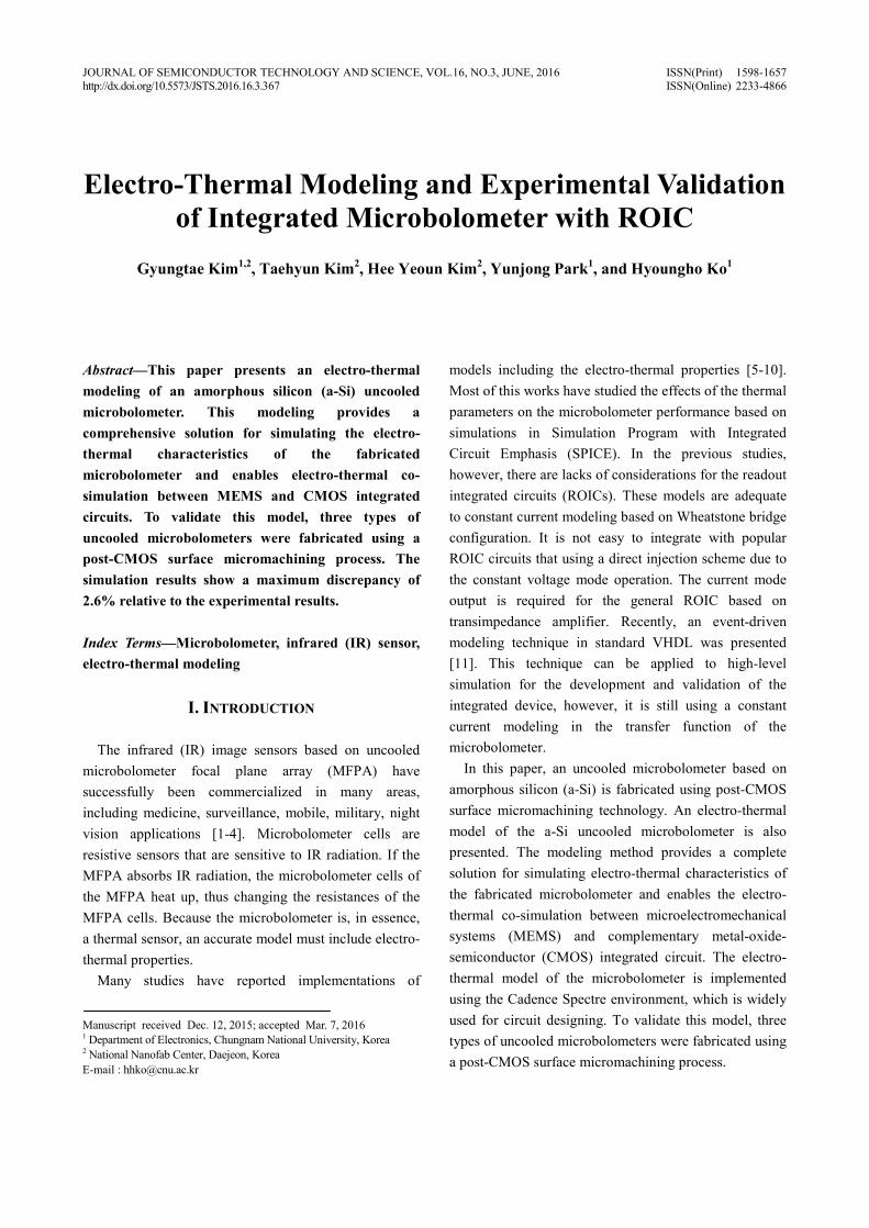
microbolometer, three types of microbolometers with a pixel size of 35 μm x 35 μm were fabricated as shown in Fig. 1. The three types of microbolometer have different supporting legs: 1) type 1 has a meshed leg structure, 2) type 2 has a normal leg structure, and 3) type 3 has a metal extended leg structure. In these three structure, the leg length and width are made equal to fix the fill factor. However in type 1, the leg was patterned with 0.7 x 0.7 μm2 holes to decrease the thermal conductance. In type 3, the leg thickness is thicker by forming the additional metal layer in which 300 nm thick metal is attached to increase the thermal conductance. The microbolometers have different heat dissipation via supporting legs. The default electrical resistance is set to 1 MΩ.
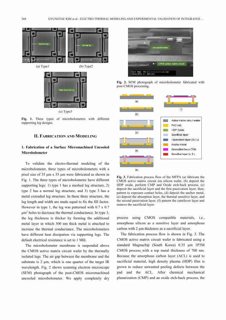
The microbolometer membrane is suspended above the CMOS active matrix circuit wafer by the thermally isolated legs. The air gap between the membrane and the substrate is 2 μm, which is one quarter of the target IR wavelength. Fig. 2 shows scanning electron microscope (SEM) photograph of the post-CMOS micromachined uncooled microbolometer. We apply completely dry
process using CMOS compatible materials, i.e., amorphous silicon as a sensitive layer and amorphous carbon with 2 μm thickness as a sacrificial layer.
The fabrication process flow is shown in Fig. 3. The CMOS active matrix circuit wafer is fabricated using a standard Magnachip (South Korea) 0.35 μm 1P3M CMOS process with a top metal thickness of 700 nm. Because the amorphous carbon layer (ACL) is used to sacrificial material, high density plasma (HDP) film is grown to reduce unwanted peeling defects between the pad and the ACL. After chemical mechanical planarization (CMP) and an oxide etch-back process, the
(a) Type1 (b) Type2
(c) Type3
Fig. 1. Three types of microbolometers with different supporting leg designs.
Fig. 2. SEM photograph of microbolometer fabricated with post-CMOS processing.
Fig. 3. Fabrication process flow of the MFPA (a) fabricate the CMOS active matrix circuit ion silicon wafer, (b) deposit the HDP oxide, perform CMP and Oxide etch-back process, (c) deposit the sacrificial layer and the first passivation layer, then, pattern to exposure contact holes, (d) deposit the anchor metal,(e) deposit the absorption layer, the thermal sensitive layer, and the second passivation layer, (f) pattern the cantilever layer and remove the sacrificial layer.
JOURNAL OF SEMICONDUCTOR TECHNOLOGY AND SCIENCE, VOL.16, NO.3, JUNE, 2016 369
sacrificial layer is deposited using the plasma-enhanced chemical vapor deposition (PECVD). The first passivation layer is deposited with 150 nm silicon nitride. Via holes of 3 μm in diameter are etched to open the metal pad using Reactive Ion Etching (RIE). After formation of via holes, the anchor metal layer with 300 nm TiN for electrical connection and the absorption layer with a 15 nm TiN film are sequentially deposited. The thermally sensitive layer is made of the boron-doped amorphous silicon with a 19 MΩ sheet resistance. Next, the second passivation layer is deposited using 150 nm silicon nitride. Then, the cantilever layer is patterned. The width and length of the membrane-supporting leg are 1.5 μm and 21 μm, respectively. The sacrificial layer was removed using an O2 plasma ashing process. Neither bending nor curling due to residual mechanical stress is observed in the fabricated microbolometers because of the multi-layer stress-compensated structure [12].
2. Parameter Extraction for an Electro-Thermal Modeling
The thermal operations of the microbolometer in time-
domain can be modeled using the thermal parameters: thermal conductance (G), heat capacitance (H) and thermal time constant [13]. Thermal conductance and heat capacitance are calculated as a summation of those of the heat elements i.e., Si3N4, TiN, and a-Si. Here, the model must take the structure of the two passivation layer and two legs of the microbolometer into account. With these parameters, the thermal time constant, τ, can be determined as
/H Gt = (1)
And the initial resistance value, R0 is determined by
the area of the exposed TiN material. This dimensions were designed to be 1.5 μm in width and 21 μm in length, the initial resistance value was calculated to be approximately 1 MΩ.
A microbolometer is a thermal sensor whose electrical resistance changes as a function of its temperature. The microbolometer’s ability to change resistance is described by its temperature coefficient of resistance (TCR) of resistance, which will be hereafter denoted by α. Typical α value for semiconductors is used to determine
resistance of a microbolometer at a given temperature as:
0 0( ) (1 [ ])R T R T Ta= - - (2)
where R0 is the microbolometer’s resistance at ambient conditions, T0 is the ambient temperature and T is the instantaneous microbolometer temperature. T-T0 will be designated by ΔT hereafter. For modeling the electro-thermal characteristics, the heat transfer equation is used:
d TH P G T
dtD
= - ×D (3)
The heat transfer equation, which is a statement of energy conservation, states that the incident power (P) equals the thermal conductance times the change in temperature, plus the heat capacity times the rate of change of temperature. Substituting P=V2/R(T) and the Eq. (2)
2
0 (1 )d T VH G T
dt R TaD
= - ×D- ´D
(4)
Appling the mathematical approximation, 1 / (1-x) will be 1+x, if the x is enough small, and rearranging, Eq. (4) can be expressed as below.
2
0 0
(1 )d T V VH G Tdt R R G
aD= - D - (5)
By comparing the Eqs. (3, 5), the change rate of thermal resistance due to the incident power or self-heating effect can be extract. If the bias voltage is applied, the thermal conductance is decreased as much as the SHF/G, and the thermal resistance (Rth) is increased by the SHF×Rth. Here, Rth is the reciprocal of thermal conductance, and the self-heating factor (SHF) is defined
Table 1. Calculated design parameters
Type 1 Type 2 Type 3 R0 1.0 MΩ 1.0 MΩ 1.1 MΩ
G [W/K] 3.0 x 10⁻⁸ 4.5 x 10⁻⁸ 9.0 x 10⁻⁸ Rth 3.3 x 10⁷ 2.2 x 10⁷ 1.1 x 10⁷
Cth [J/K] 4.0 x 10⁻¹⁰ 4.0 x 10⁻¹⁰ 4.0 x 10⁻¹⁰ gm 9.8 x 10⁻⁸ 6.2 x 10⁻⁸ 2.7 x 10⁻⁸
370 GYUNGTAE KIM et al : ELECTRO-THERMAL MODELING AND EXPERIMENTAL VALIDATION OF INTEGRATED …
as α×V2/R0. This extracted SHF is a key parameter of the proposed electro-thermal model, and we have confirmed that the thermal resistance is changed in proportion to the square of the applied bias in chapter 3. The effect of self-heating due to applied bias is also an important consideration in uncooled microbolometer because it reflects responsivity and the trend of the signal with increasing bias voltage. The current difference due to self-heating effect, gm is expressed as
m E thg i SHF R= ´ ´ (6)
where iE is initial electrical current at ambient temperature, and calculated by V/R0. The electro-thermal parameters extracted from the fabricated uncooled microbolometer are summarized in Table 1.
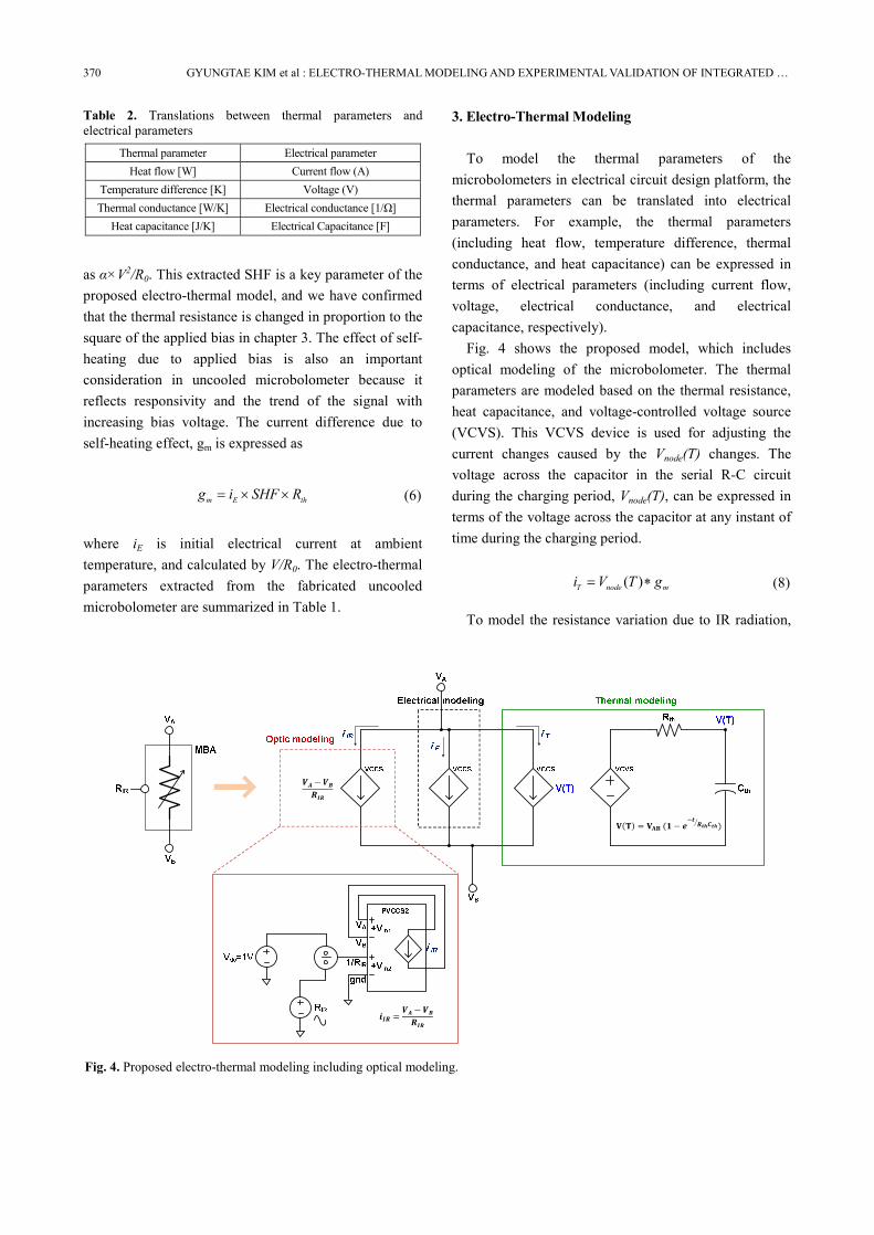
3. Electro-Thermal Modeling To model the thermal parameters of the
microbolometers in electrical circuit design platform, the thermal parameters can be translated into electrical parameters. For example, the thermal parameters (including heat flow, temperature difference, thermal conductance, and heat capacitance) can be expressed in terms of electrical parameters (including current flow, voltage, electrical conductance, and electrical capacitance, respectively).
Fig. 4 shows the proposed model, which includes optical modeling of the microbolometer. The thermal parameters are modeled based on the thermal resistance, heat capacitance, and voltage-controlled voltage source (VCVS). This VCVS device is used for adjusting the current changes caused by the Vnode(T) changes. The voltage across the capacitor in the serial R-C circuit during the charging period, Vnode(T), can be expressed in terms of the voltage across the capacitor at any instant of time during the charging period.
( )T node mi V T g= * (8)
To model the resistance variation due to IR radiation,
Table 2. Translations between thermal parameters and electrical parameters
Thermal parameter Electrical parameter Heat flow [W] Current flow (A)
Temperature difference [K] Voltage (V) Thermal conductance [W/K] Electrical conductance [1/Ω]
Heat capacitance [J/K] Electrical Capacitance [F]
Fig. 4. Proposed electro-thermal modeling including optical modeling.
JOURNAL OF SEMICONDUCTOR TECHNOLOGY AND SCIENCE, VOL.16, NO.3, JUNE, 2016 371
optical modeling component is added. This model must be included in the sub-circuit of the VCCS like the thermal model. But it is separately located for user-friendly environment. Designer can easily simulate by controlling IR radiation value. The Optical modeling is implemented by using the two-input polynomial voltage-controlled current source (PVCCS2), a functional divider, and a voltage source of the functional library in Cadence Virtuoso. The PVCCS2 represents a current source with an output current value that is a polynomial function of the voltages across the pairs of controlling input ports.
The following equation describes the current through the source as a function of time.
2
1 2 1 3 2 4 1
25 1 2 6 2
OUT in in in
in in in
I p p V p V p Vp V V p V
= + × + × + ×
+ × × + × (9)
where the coefficients pi are the polynomial parameter value, Vin1 and Vin2 are the voltage across the first pair of input ports and the second pair of input ports, respectively. The resistance value, RIR, indicates the response due to IR radiation, which is applied as a sine wave for electro-thermal simulation. Substituting the polynomial coefficients parameter value of p5 is equal to 1, output current is expressed as ( ) /IR A B IRI V V R= - (10)
The total current, I, through the microbolometer is
expressed as a sum of the electrical current, iE, the thermal current, iT and optical current, iIR.
E T IRI I I I= + + (11)
4. Simulation Results of the Proposed Modeling
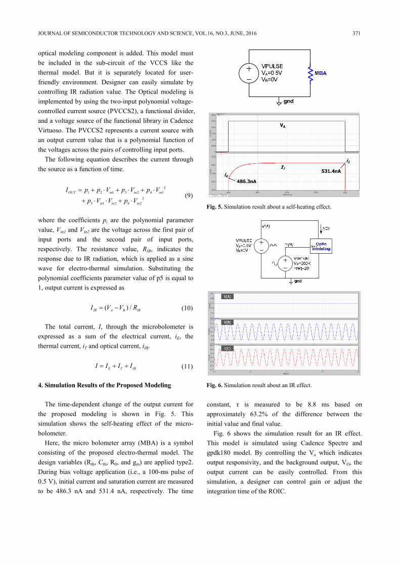
The time-dependent change of the output current for
the proposed modeling is shown in Fig. 5. This simulation shows the self-heating effect of the micro- bolometer.
Here, the micro bolometer array (MBA) is a symbol consisting of the proposed electro-thermal model. The design variables (Rth, Cth, R0, and gm) are applied type2. During bias voltage application (i.e., a 100-ms pulse of 0.5 V), initial current and saturation current are measured to be 486.3 nA and 531.4 nA, respectively. The time
constant, τ is measured to be 8.8 ms based on approximately 63.2% of the difference between the initial value and final value.
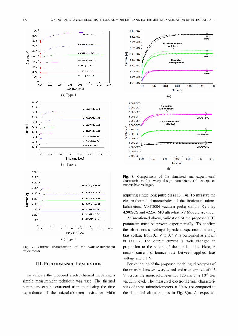
Fig. 6 shows the simulation result for an IR effect. This model is simulated using Cadence Spectre and gpdk180 model. By controlling the Va which indicates output responsivity, and the background output, VO, the output current can be easily controlled. From this simulation, a designer can control gain or adjust the integration time of the ROIC.
Fig. 5. Simulation result about a self-heating effect.
Fig. 6. Simulation result about an IR effect.
372 GYUNGTAE KIM et al : ELECTRO-THERMAL MODELING AND EXPERIMENTAL VALIDATION OF INTEGRATED …
III. PERFORMANCE EVALUATION
To validate the proposed electro-thermal modeling, a simple measurement technique was used. The thermal parameters can be extracted from monitoring the time dependence of the microbolometer resistance while
adjusting single long pulse bias [13, 14]. To measure the electro-thermal characteristics of the fabricated micro- bolometers, MST8000 vacuum probe station, Keithley 4200SCS and 4225-PMU ultra-fast I-V Module are used.
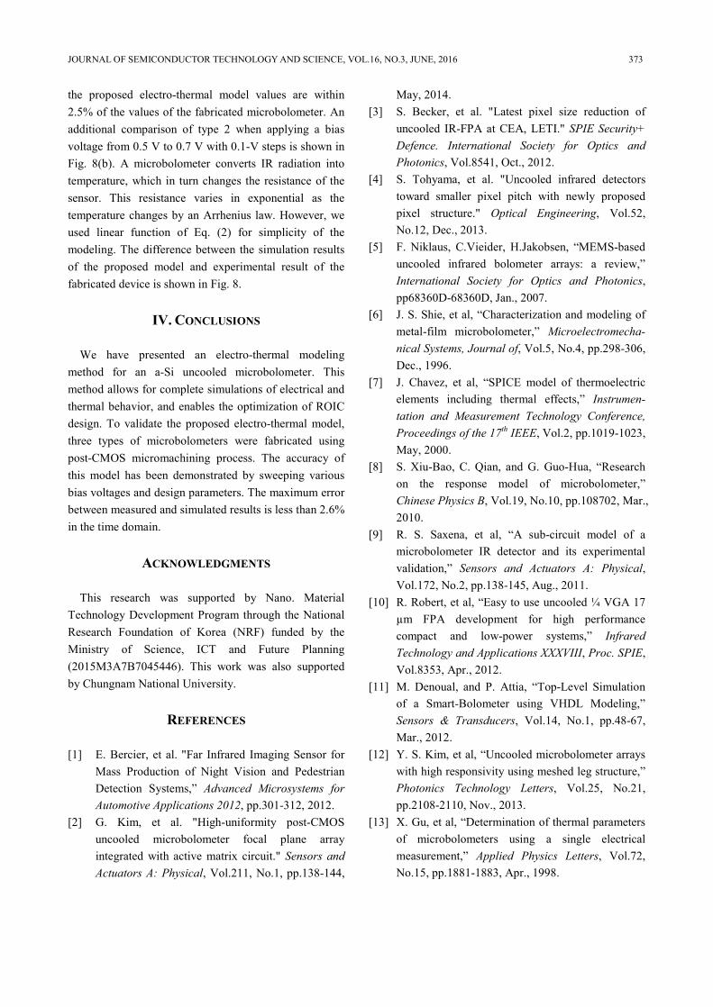
As mentioned above, validation of the proposed SHF parameter must be proven experimentally. To confirm this characteristic, voltage-dependent experiments altering bias voltage from 0.1 V to 0.7 V is performed as shown in Fig. 7. The output current is well changed in proportion to the square of the applied bias. Here, Δ means current difference rate between applied bias voltage and 0.1 V.
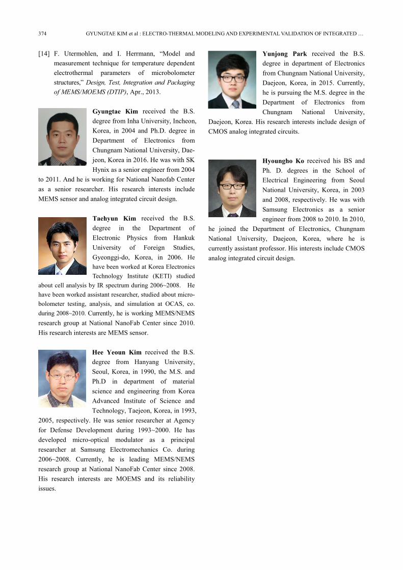
For validation of the proposed modeling, three types of the microbolometers were tested under an applied of 0.5 V across the microbolometer for 120 ms at a 10-5 torr vacuum level. The measured electro-thermal characteri- stics of these microbolometers at 300K are compared to the simulated characteristics in Fig. 8(a). As expected,
(a) Type 1
(b) Type 2
(c) Type 3
Fig. 7. Current characteristic of the voltage-dependent experiments.
(a)
(b)
Fig. 8. Comparisons of the simulated and experimental characteristics (a) sweep design parameters, (b) sweeps of various bias voltages.
JOURNAL OF SEMICONDUCTOR TECHNOLOGY AND SCIENCE, VOL.16, NO.3, JUNE, 2016 373
the proposed electro-thermal model values are within 2.5% of the values of the fabricated microbolometer. An additional comparison of type 2 when applying a bias voltage from 0.5 V to 0.7 V with 0.1-V steps is shown in Fig. 8(b). A microbolometer converts IR radiation into temperature, which in turn changes the resistance of the sensor. This resistance varies in exponential as the temperature changes by an Arrhenius law. However, we used linear function of Eq. (2) for simplicity of the modeling. The difference between the simulation results of the proposed model and experimental result of the fabricated device is shown in Fig. 8.
IV. CONCLUSIONS
We have presented an electro-thermal modeling method for an a-Si uncooled microbolometer. This method allows for complete simulations of electrical and thermal behavior, and enables the optimization of ROIC design. To validate the proposed electro-thermal model, three types of microbolometers were fabricated using post-CMOS micromachining process. The accuracy of this model has been demonstrated by sweeping various bias voltages and design parameters. The maximum error between measured and simulated results is less than 2.6% in the time domain.
ACKNOWLEDGMENTS
This research was supported by Nano. Material Technology Development Program through the National Research Foundation of Korea (NRF) funded by the Ministry of Science, ICT and Future Planning (2015M3A7B7045446). This work was also supported by Chungnam National University.
REFERENCES
[1] E. Bercier, et al. "Far Infrared Imaging Sensor for Mass Production of Night Vision and Pedestrian Detection Systems,” Advanced Microsystems for Automotive Applications 2012, pp.301-312, 2012.
[2] G. Kim, et al. "High-uniformity post-CMOS uncooled microbolometer focal plane array integrated with active matrix circuit." Sensors and Actuators A: Physical, Vol.211, No.1, pp.138-144,
May, 2014. [3] S. Becker, et al. "Latest pixel size reduction of
uncooled IR-FPA at CEA, LETI." SPIE Security+ Defence. International Society for Optics and Photonics, Vol.8541, Oct., 2012.
[4] S. Tohyama, et al. "Uncooled infrared detectors toward smaller pixel pitch with newly proposed pixel structure." Optical Engineering, Vol.52, No.12, Dec., 2013.
[5] F. Niklaus, C.Vieider, H.Jakobsen, “MEMS-based uncooled infrared bolometer arrays: a review,” International Society for Optics and Photonics, pp68360D-68360D, Jan., 2007.
[6] J. S. Shie, et al, “Characterization and modeling of metal-film microbolometer,” Microelectromecha- nical Systems, Journal of, Vol.5, No.4, pp.298-306, Dec., 1996.
[7] J. Chavez, et al, “SPICE model of thermoelectric elements including thermal effects,” Instrumen- tation and Measurement Technology Conference, Proceedings of the 17th IEEE, Vol.2, pp.1019-1023, May, 2000.
[8] S. Xiu-Bao, C. Qian, and G. Guo-Hua, “Research on the response model of microbolometer,” Chinese Physics B, Vol.19, No.10, pp.108702, Mar., 2010.
[9] R. S. Saxena, et al, “A sub-circuit model of a microbolometer IR detector and its experimental validation,” Sensors and Actuators A: Physical, Vol.172, No.2, pp.138-145, Aug., 2011.
[10] R. Robert, et al, “Easy to use uncooled ¼ VGA 17 µm FPA development for high performance compact and low-power systems,” Infrared Technology and Applications XXXVIII, Proc. SPIE, Vol.8353, Apr., 2012.
[11] M. Denoual, and P. Attia, “Top-Level Simulation of a Smart-Bolometer using VHDL Modeling,” Sensors & Transducers, Vol.14, No.1, pp.48-67, Mar., 2012.
[12] Y. S. Kim, et al, “Uncooled microbolometer arrays with high responsivity using meshed leg structure,” Photonics Technology Letters, Vol.25, No.21, pp.2108-2110, Nov., 2013.
[13] X. Gu, et al, “Determination of thermal parameters of microbolometers using a single electrical measurement,” Applied Physics Letters, Vol.72, No.15, pp.1881-1883, Apr., 1998.
374 GYUNGTAE KIM et al : ELECTRO-THERMAL MODELING AND EXPERIMENTAL VALIDATION OF INTEGRATED …
[14] F. Utermohlen, and I. Herrmann, “Model and measurement technique for temperature dependent electrothermal parameters of microbolometer structures,” Design, Test, Integration and Packaging of MEMS/MOEMS (DTIP), Apr., 2013.
Gyungtae Kim received the B.S. degree from Inha University, Incheon, Korea, in 2004 and Ph.D. degree in Department of Electronics from Chungnam National University, Dae- jeon, Korea in 2016. He was with SK Hynix as a senior engineer from 2004
to 2011. And he is working for National Nanofab Center as a senior researcher. His research interests include MEMS sensor and analog integrated circuit design.
Taehyun Kim received the B.S. degree in the Department of Electronic Physics from Hankuk University of Foreign Studies, Gyeonggi-do, Korea, in 2006. He have been worked at Korea Electronics Technology Institute (KETI) studied
about cell analysis by IR spectrum during 2006~2008. He have been worked assistant researcher, studied about micro-bolometer testing, analysis, and simulation at OCAS, co. during 2008~2010. Currently, he is working MEMS/NEMS research group at National NanoFab Center since 2010. His research interests are MEMS sensor.
Hee Yeoun Kim received the B.S. degree from Hanyang University, Seoul, Korea, in 1990, the M.S. and Ph.D in department of material science and engineering from Korea Advanced Institute of Science and Technology, Taejeon, Korea, in 1993,
2005, respectively. He was senior researcher at Agency for Defense Development during 1993~2000. He has developed micro-optical modulator as a principal researcher at Samsung Electromechanics Co. during 2006~2008. Currently, he is leading MEMS/NEMS research group at National NanoFab Center since 2008. His research interests are MOEMS and its reliability issues.
Yunjong Park received the B.S. degree in department of Electronics from Chungnam National University, Daejeon, Korea, in 2015. Currently, he is pursuing the M.S. degree in the Department of Electronics from Chungnam National University,
Daejeon, Korea. His research interests include design of CMOS analog integrated circuits.
Hyoungho Ko received his BS and Ph. D. degrees in the School of Electrical Engineering from Seoul National University, Korea, in 2003 and 2008, respectively. He was with Samsung Electronics as a senior engineer from 2008 to 2010. In 2010,
he joined the Department of Electronics, Chungnam National University, Daejeon, Korea, where he is currently assistant professor. His interests include CMOS analog integrated circuit design.