ELECTRO-THERMAL SIMULATION STUDIES OF...
68
ELECTRO-THERMAL SIMULATION STUDIES OF SINGLE-EVENT BURNOUT IN POWER DIODES By Sameer V. Mahajan Thesis Submitted to the Faculty of the Graduate School of Vanderbilt University in partial fulfillment of the requirements for the degree of MASTER OF SCIENCE in Interdisciplinary Materials Science August, 2006 Nashville, Tennessee Approved: Professor D. Greg Walker Professor Ronald D. Schrimpf
-
Upload
vuongthuan -
Category
Documents
-
view
215 -
download
1
Transcript of ELECTRO-THERMAL SIMULATION STUDIES OF...
ELECTRO-THERMAL SIMULATION STUDIES OF
SINGLE-EVENT BURNOUT IN POWER DIODES
By
Sameer V. Mahajan
Thesis
Submitted to the Faculty of the
Graduate School of Vanderbilt University
in partial fulfillment of the requirements
for the degree of
MASTER OF SCIENCE
in
Interdisciplinary Materials Science
August, 2006
Nashville, Tennessee
Approved:
Professor D. Greg Walker
Professor Ronald D. Schrimpf

ii
ACKNOWLEDGEMENTS
I express my utmost gratitude towards Prof. Greg Walker for providing me an
opportunity to work with him on this project. I am grateful to him for his guidance and
encouragement at various phases of this project. Special word of thanks goes to Prof.
Ronald Schrimpf for his invaluable guidance during this work and important thoughts at
all stages.
I would like to thank Dr. Marek Turowski and Ashok Raman for their help on simulation
models using CFD-ACE+ simulation software. I would like to mention my colleagues,
Aniruddha Marathe, Anuradha Bulusu, Dr. Aditya Karmarkar and Dr. Abdulrahman Al-
Badri, with whom I had fruitful discussions on certain aspects of this work.
iii
TABLE OF CONTENTS
ACKNOWLEDGEMENTS................................................................................................ ii LIST OF TABLES.............................................................................................................. v LIST OF FIGURES ........................................................................................................... vi Chapter I. INTRODUCTION........................................................................................................... 1
Burnout mechanism in power MOSFETs....................................................................... 2 Burnout of power diodes................................................................................................. 2 Scope and organization of the thesis............................................................................... 6
II. DIODE THEORY .......................................................................................................... 9
Structure of a diode......................................................................................................... 9 Basic Device Characteristics......................................................................................... 10
Diode at Thermal Equilibrium.................................................................................. 11 Forward Bias Condition............................................................................................ 13 Reverse Bias Condition............................................................................................. 15
III. CHARGE AND ENERGY TRANSPORT IN SEMICONDUCTORS...................... 17
Drift-Diffusion Model................................................................................................. 17 Poisson’s Equation.................................................................................................... 18 Carrier Continuity Equations .................................................................................... 18 Current Equations ..................................................................................................... 18
Lattice Energy Model ................................................................................................. 19 Carrier Movement in Semiconductors ........................................................................ 20
Carrier Drift .............................................................................................................. 21 Carrier Diffusion....................................................................................................... 22
Excess Carriers in Semiconductors............................................................................. 23 Recombination .......................................................................................................... 23
Shockley-Read-Hall Recombination .................................................................... 24 Auger Recombination ........................................................................................... 25
Generation................................................................................................................. 27 Impact Ionization .................................................................................................. 27 Ion strike induced carriers..................................................................................... 29
IV. SIMULATIONS AND RESULTS ............................................................................. 31
Diode Structure ........................................................................................................... 31 Device Implementation and Simulation Methodology ............................................... 32
iv
Steady-state Simulations.............................................................................................. 36 Transient Simulations .................................................................................................. 38
Effect of an ion strike on diode current .................................................................... 40 Role of impact ionization model in ion strike simulations ....................................... 42 Effect of temperature on strike-induced current transients....................................... 45 Non-isothermal ion strike simulation........................................................................ 47
V. CONCLUSION............................................................................................................ 56 REFERENCES ................................................................................................................. 59
v
LIST OF TABLES
Table Page 1 Charge collected in different time after ion strike .................................................... 47

vi
LIST OF FIGURES
Figure Page 1 Secondary charge generation fraction vs applied bias for different ion-energies
[14] .............................................................................................................................. 4
2 Simulation of the spatial and temporal evolution of the internal electric field in a 4 kV diode for C12 (17 MeV) ion. Applied bias = 1800 V [15].................................. 5
3 Structure of a diode. .................................................................................................. 10
4 pn junction at thermal equilibrium............................................................................ 12
5 Band diagrams showing formation of a pn junction. ................................................ 12
6 Forward biased pn junction....................................................................................... 14
7 Forward bias characteristics of a diode..................................................................... 14
8 Reverse biased pn junction. ...................................................................................... 15
9 Reverse bias characteristics of a diode. .................................................................... 16
10 Shockley-Read-Hall recombination process in a semiconductor. ............................ 24
11 Auger recombination process in a semiconductor. ................................................... 26
12 Impact ionization ...................................................................................................... 28
13 Simulated diode structure showing doping............................................................... 32
14 Diode structure showing refined mesh near junctions and along ion path. .............. 33
15 Diode structure showing boundary conditions. Symmetry condition indicates no carrier and heat flow across the boundary. ............................................................... 35
16 Built-in potential across the diode at equilibrium..................................................... 36
17 Simulated reverse bias characteristics for the power diode structure ....................... 37
18 Schematic of track structure modeled in 2-D ion-strike simulations........................ 39
19 Density of strike-induced electron-hole pairs deposited in time indicating complete charge deposition within first 5 ps (in red). Transient current following this charge deposition is also plotted (-4000 V, LET= 0.71). .................. 41
vii
20 Contribution of avalanche-induced charge on current transients through diode after strike ................................................................................................................. 43
21 Current flowing through the diode only due to avalanche-induced charge. ............. 44
22 Current transients for applied biases of 2900 V, 3500 V and 4000 V ...................... 45
23 Effect of temperature on current transients simulated at 300 K, 400 K and 500 K................................................................................................................................ 46
24 Comparison of current transients with and without self-heating effects at 4000 V applied bias. .......................................................................................................... 49
25 Temperature distribution near pn junction at 32 ns after strike at 4000 V. .............. 49
26 Current transients with inclusion of self-heating effects for 2900 V, 3500 V, and 4000 V....................................................................................................................... 51
27 Electric field at a distance from p+-n- interface inside n- region in the plane of incident ion (4000 V case) ........................................................................................ 52
28 Electron density at a distance from p+-n- interface inside n- region in the plane of incident ion (4000 V case).................................................................................... 52
29 Peak temperatures inside the device at different time after the strike for applied biases of 2900 V, 3500 V and 4000 V. Same plot on linear time scale is shown in the inset. ................................................................................................................ 53
30 Normalized carrier concentration inside 2D rectangular diode away from the axis of ion strike at different times............................................................................ 55
31 Normalized carrier concentration inside 2D axi-symmetric diode away from the axis of ion strike at different times............................................................................ 55
1
CHAPTER I
INTRODUCTION
Electronic systems positioned in space are exposed to various forms of radiation. The
space radiation environment consists of solar rays, cosmic rays and protons and electrons
trapped in radiation belts [1, 2]. Interaction of electronic systems with ionizing radiation
could affect their performance, leading to premature failure. Reliability of these
electronic systems is very important because of the high costs of space systems. A
complete understanding of fundamental mechanisms of failure in electronic systems is
necessary to improve their reliability.
A single-event effect (SEE) can be defined as the temporary or permanent failure of an
electronic device due to interaction with an energetic particle. Single-event effects have
been observed in a variety of space as well as terrestrial electronic systems [3, 4]. Solar
rays and heavy ions are mainly responsible for the failures in space systems, while
neutrons, protons, and pions cause failures in terrestrial systems. Single-event burnout
(SEB) is a type of single-event effect, which is characterized by a permanent failure
caused by physical damage.
Power devices (high current, high voltage devices) are widely used in space-based
electronic systems. The very large electric fields present in power devices could prove
lethal when an ionizing particle creates a dense filament of electron-hole pairs.

2
Burnout mechanism in power MOSFETs
SEB in power metal-oxide-semiconductor field-effect transistor (MOSFET) system was
noticed by Waskiewicz et al [5]. Considerable effort has been devoted to understanding
breakdown mechanisms in n-channel MOSFETs with experimental [6-8] and simulation
techniques [9]. The parasitic npn bipolar structure inherent to n-channel MOSFETs was
identified to play a key role in the burnout mechanism. The drain-substrate junction is
reverse-biased in n-channel MOSFETs. When an energetic particle passes through the
junction, the generated electron-hole pairs separate under the influence of the electric
field, producing current. The current across the reverse-biased junction may turn on the
parasitic npn transistor. The resulting large currents and high voltages may generate high
power, leading to burnout of the MOSFET.
Burnout of power diodes
Catastrophic failures in power diodes were first observed by Kabza when DC stress tests
were performed on power diodes operating at rated conditions [10]. When the same tests
were performed 140 m below ground, failure rates dropped significantly. Cosmic
radiation was identified as a cause of failures. The failure rate was exponentially
dependent on applied bias. Simulation studies predicted high avalanche-generated charge
compared to deposited charge for high voltages. Thus high local power densities causing
localized self-heating leading to burnout were thought to be responsible for failures.
Current transients were simulated for different numbers of strike-induced carriers.
Simulations indicated that peak temperature inside the device exceeds the silicon melting
temperature above a total number of 5 × 10¹⁰ strike-induced electron-hole pairs within the
3
track creating high carrier density. A particle possessing 180 GeV is required to generate
this number of carriers. However, particle rates for these energies are lower than
observed failure rates. Thus it was found that solely radiation-induced charges do not
predict device failure due to self-heating. Zeller developed a phenomenological model
describing the failure rate based on its exponential dependence on applied bias [11]. This
model produced a good fit with the experimental data, indicating its applicability for
device design. The burnout mechanism was still unidentified. The thermal runaway
phenomenon was reported in 2-D simulation studies of non-planar GTO-Thyristors while
studying the effects of different cooling conditions [12]. A thermodynamic model of
thermoelectric transport predicted accelerated thermal runaway process.
Voss et al. performed irradiation experiments with C12 ions possessing different energies
[13]. Irradiation was started at 2000 V of blocking voltage, and applied bias was
increased 100 V per minute of exposure. All the devices failed due to irradiation. Charge
collection spectra taken during the study indicated noticeable charge multiplication above
2400 V. The failures were attributed to triggering of nuclear reactions in the device, not
necessarily near the pn junction.
Busatto et al. studied single-event burnout in power diodes using bombardment of Si28
ions possessing energies of 108 MeV and 156 MeV [14]. Charge collection and current
traces for the diode were recorded. Deposited charge was independent of applied bias, but
secondary charge generation was found to be dependent on the applied bias. Also, a
secondary increase in collected charge was different for ions possessing different

4
energies. Initiation of secondary charge collection was found to be dependent on the
energy of the ion. Figure 1 shows fraction of secondary charge generation as a function of
applied bias for two different ion energies (108 MeV and 156 MeV). It was found that
higher applied voltage is necessary to generate same secondary charge fraction for more
energetic ions. For example, 70% of the total secondary charge is estimated to be
generated at the applied bias of 780 V for 108 MeV ions, while for 156 MeV ions the
diode needs to be biased at 955 V (refer Figure 1).
Figure 1 Secondary charge generation fraction vs. applied bias for different ion-energies [14].
Another study was performed by Soelkar et al. with bombardment of high energy carbon
and Krypton ions; current waveforms and charge spectra were recorded [15]. The
generated charge was found to be dependent on bias. The current trace for proton-
irradiated samples indicated secondary current that was associated with thermal
breakdown [15]. However, the thermal breakdown mechanism was not confirmed with

5
further analysis. 2-D axi-symmetric electrical simulations were performed to observe the
internal electric field evolution after the strike. Figure 2 shows spatial and temporal
profile of electric field along diode depth in the ion incident plane. The range of C12 ion
(17 MeV) is short (16 µm) compared to diode depth (450 µm). Deposited charge density
increases along the ion track, which peaks at the end of the track. The charges deposited
during the strike modify the potential distribution. This results in localized electric field
variation. The electric field peak occurs at the end of the ion track. The charges move
towards the contacts because of drift and in radial direction due to the diffusion. Thus the
electric field peak moves to the cathode as the carrier distribution changes along the ion
path. The peak electric field diminishes in time as carriers are swept out of the diode and
carrier distribution moves towards steady state equilibrium.
Figure 2 Simulation of the spatial and temporal evolution of the internal electric field in a 4 kV diode for C12 (17 MeV) ion. Applied bias = 1800 V [15].
Ironically, diodes are generally much simpler devices than MOSFETs, yet understanding
of SEB in these elementary devices is limited. The inherent bipolar structures responsible
6
for failure in power MOSFETs do not exist in diodes [16]. There is no corresponding
electrical feedback mechanism to maintain a strike-induced current until the device
destroys itself.
The experimental and simulation studies performed so far have failed to identify the
burnout breakdown mechanism for power diodes. Although the possibility of thermal
breakdown has been suggested with preliminary results, enough attention has not been
given to the thermal effects. Recently, Al-Badri et al observed single event burnout of
power diode using coupled electro-thermal simulations [17]. The effect of irradiation of
17-MeV C12 ions was simulated. When diode was biased at 2700 V and above, large
increase in the current along with temperature rise reaching melting point of silicon was
observed indicating diode burnout. The breakdown is attributed to the local heat
generation due to impact ionization-generated charge. Presence of thermal feedback loop
is hypothesized earlier [18]. Local temperatures inside diode increase due to presence of
high current and electric field following ion strike. Intrinsic carrier concentration, which
is also a function of temperature, increases with temperature. As the intrinsic carrier
concentration increases at high temperatures, more carriers are available, producing large
current. A thermal feedback loop may be initiated where an increase in current leads to
more heating.
Scope and organization of the thesis
The goal of the present work is to identify the burnout mechanism in power diodes using
electrical-thermal simulations. A simplified 2-D power diode structure is modeled for
7
which single-event burnout was observed experimentally. Coupled electro-thermal
simulations that include thermal effects are performed. Temperature-dependent mobility,
recombination and intrinsic carrier concentration are employed. The simulation technique
enables isolation of impact ionization to identify its contribution in strike-induced
current. Also, the effect of applied bias on strike-induced current is studied at three
different applied biases. Isothermal ion-strike simulations at different temperature are
performed to understand the effect of temperature on the ion-induced current transient.
Non-isothermal ion-strike simulations on the power diode at different applied biases are
performed. Peak temperature inside the power diode is monitored in time. The results are
compared with the published data and analyzed to explain the breakdown of the diode.
Chapter I of the thesis introduces the single-event burnout phenomenon observed in
power devices such as power MOSFETS and power diodes. Experimental and simulation
studies performed by the scientific community to identify failure mechanisms are
summarized. Chapter II covers the fundamental physics describing pn-junction diodes.
The steady-state electrical characteristics of diode are described with the help of
supporting device-physics concepts. In Chapter III, various non-equilibrium phenomena
that may occur during semiconductor device operation are discussed. The carrier and
energy transport mechanisms that explain motion of the carriers under non-equilibrium
conditions are reviewed. Chapter IV includes the simulation methodology followed for
modeling the power diode. Various isothermal and non-isothermal simulations performed
in a logical pattern to study the single-event burnout mechanism are listed; the results are

8
discussed and compared with reported data wherever possible. The results of the
simulation studies are summarized in Chapter V.
9
CHAPTER II
DIODE THEORY
A pn junction is a component of most microelectronic devices. A diode is the simplest
device, having a single pn junction, while many other devices have multiple pn junctions.
In the present work, single-event burnout in power diodes is investigated primarily with
simulated temporal electrical characteristics.
First, the structure of a diode and its electrical characteristics under different operating
modes are discussed [19]. The electrical characteristics of a diode are explained in depth
with device physics concepts. It is necessary to understand the physics of a diode under
different operating modes.
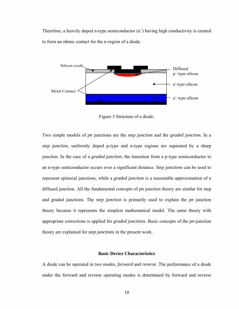
Structure of a diode
Essentially, a diode has a single pn junction that is formed when p-type and n-type
semiconductors are joined physically. A p-type semiconductor with excess holes is
obtained by addition of acceptor impurity ions, while an n-type semiconductor with
excess electrons is formed by addition of donor impurity ions. A typical structure of a
diode is shown in Figure 3. Here, a pn junction is formed between diffused p-type (p+)
and epitaxial n-type (n-) regions. The plus (+) and minus (-) signs represent heavily and
lightly doped semiconductors respectively. High conductivity is necessary near a metal
contact to form an Ohmic contact. Lightly doped semiconductors have low conductivity.
10
Therefore, a heavily doped n-type semiconductor (n+) having high conductivity is created
to form an ohmic contact for the n-region of a diode.
Figure 3 Structure of a diode.
Two simple models of pn junctions are the step junction and the graded junction. In a
step junction, uniformly doped p-type and n-type regions are separated by a sharp
junction. In the case of a graded junction, the transition from a p-type semiconductor to
an n-type semiconductor occurs over a significant distance. Step junctions can be used to
represent epitaxial junctions, while a graded junction is a reasonable approximation of a
diffused junction. All the fundamental concepts of pn junction theory are similar for step
and graded junctions. The step junction is primarily used to explain the pn junction
theory because it represents the simplest mathematical model. The same theory with
appropriate corrections is applied for graded junctions. Basic concepts of the pn-junction
theory are explained for step junctions in the present work.
Basic Device Characteristics
A diode can be operated in two modes, forward and reverse. The performance of a diode
under the forward and reverse operating modes is determined by forward and reverse
Diffused p+-type silicon
n--type silicon
n+-type silicon
Silicon oxide
Metal Contact

11
electrical characteristics respectively. First, a diode under equilibrium conditions is
discussed. Next, forward and reverse characteristics are explained with the support of
device physics.
Diode at Thermal Equilibrium
n- and p-type semiconductors have a large concentration of free electrons and holes,
respectively. Both the semiconductors are neutral in the bulk region. One carrier is
present for each ionized impurity atom in the bulk semiconductor material. Electrons
from the n-type semiconductor diffuse into the p-type semiconductor due to a significant
difference in electron concentration. The reduced electron concentration leaves behind
positive impurity ions near the junction. Likewise, negative impurity ions are left near the
junction when holes from p-type material diffuse across the junction to n-type material.
Thus, a space charge region is developed near the metallurgical junction, where positive
impurity ions are on the n-side of the junction and negative impurity ions are on the p-
side of the junction. This region is also called the depletion region because of the low
number of free electrons and holes. An electric field, E, is created in the depletion region
and a potential barrier is formed. The direction of the electric field is opposite the
diffusion current. The electrons and holes diffuse across the junction until the magnitude
of the electric field is increased to the level where electrons and holes have insufficient
energy to overcome this barrier. The resulting potential difference is called the built-in
voltage, φi, and no net current flows across the junction. The pn junction is said to be in
thermal equilibrium at this point as shown in Figure 4.

12
Figure 4 pn junction at thermal equilibrium.
The energy band diagram of a pn junction is sketched in Figure 5. Here Ec represents the
conduction band edge, Ev represents the valence band edge, and Efn and Efp represent the
Fermi levels of the n- and p-type semiconductors, respectively.
Figure 5 Band diagrams showing formation of a pn junction.
Ec
Ev
Efp
P-region
Ec
Efn
Ev
N-region
(a)
Ec
Ev
Efn Efp
qφo
(b)
P-region Depletion width
N-region
hole
electron
Negative ion
Positive ion
13
The built-in voltage of a pn junction depends on donor atom concentration, Nd in the n-
region and acceptor atom concentration, Na in the p-region, which can be calculated
analytically from the following equation [19].
)ln( 2i
daBi n
NNqT ×
=κ
φ (1)
where κB is Boltzmann’s constant, q is the charge of an electron, T is temperature and ni
is the intrinsic carrier concentration. The depletion region width, Xd, is analytically
calculated by the following equation, where εs is the permittivity of the semiconductor.
21
112 ⎥⎦
⎤⎢⎣
⎡⎟⎟⎠
⎞⎜⎜⎝
⎛+=
dai
sd NNq
X φε
(2)
Forward Bias Condition
A pn junction operates in the forward mode when positive bias is applied to the p-region
with respect to n-region. The majority carriers in each region move towards the junction
and neutralize some of the space charge as seen in Figure 6. The depletion width is
reduced and the potential barrier is lowered during the forward bias mode causing a
decrease in resistance to the current flow across the junction. The electrons from the n-
region overcome the barrier and enter the p-region where they recombine with holes.
Similarly, holes from the p-region cross the barrier and enter the n-region where they
recombine with electrons.

14
Figure 6 Forward biased pn junction.
In forward bias, the current across the junction increases as positive bias is applied to the
p-region. Figure 7 shows typical forward bias characteristics.
Figure 7 Forward bias characteristics of a diode.
Bias
Current
Built-in
P-region
Original
Depletion width N-region
Depletion width

15
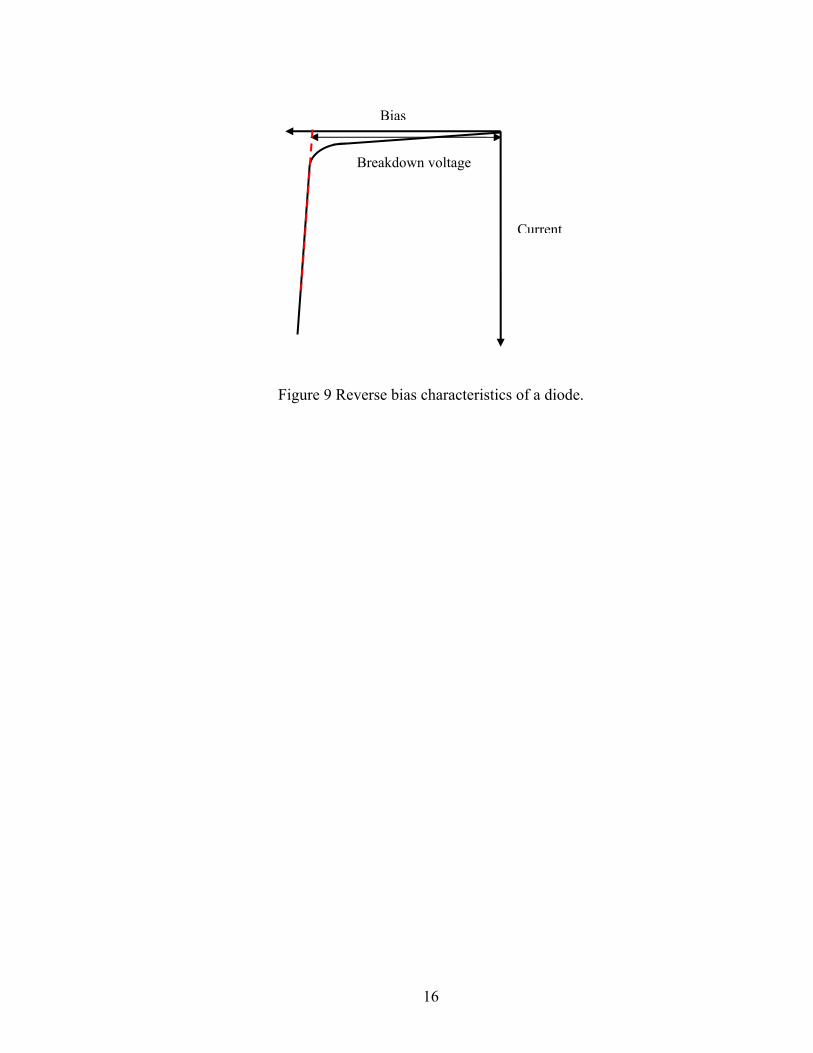
Reverse Bias Condition
The reverse bias condition is achieved when negative voltage is applied to the p-region
with respect to the n-region as seen in Figure 8. The majority carriers in each region are
attracted away from the junction by the contacts. This leads to increased depletion width
and higher potential barrier, which prevents flow of current across the junction due to
majority carriers. However, a small current flows across the junction due to the flow of
minority carriers across the junction under the applied bias.
Figure 8 Reverse biased pn junction.
The current across the junction is plotted as a function of reverse bias in Figure 9. One
important feature of the reverse bias characteristics is the breakdown voltage, the voltage
above which a diode conducts high current in the reverse mode.
P-region N-region
Original
Depletion width
Depletion width
16
Figure 9 Reverse bias characteristics of a diode.
Bias
Current
Breakdown voltage
17
CHAPTER III
CHARGE AND ENERGY TRANSPORT IN SEMICONDUCTORS
The Schrödinger wave equation is the most accurate way of explaining the motion of the
charge carriers in semiconductors. However, obtaining the device characteristics with
wave theory is extremely tedious. The wave theory concept needs to be applied when the
carrier transport in the nanoscale semiconductors is considered. Transport theories are
utilized to solve for the carrier transport in microscale devices, which consider the
carriers as particles possessing related properties such as mass, momentum and energy.
Drift-Diffusion Model
The drift-diffusion model is predominantly used to describe the transport of charge
carriers (electrons and holes) in semiconductor devices. The drift-diffusion model is
formulated with the conservation of particle density and momentum balance, but the
energy balance model is neglected. The temperature of the carriers is assumed to be that
of the lattice temperature, which is usually set as ambient temperature. Thus, the effect of
temperature on device parameters is not incorporated when the drift-diffusion model is
used solely. However, the lattice energy equation can be solved self-consistently with the
drift-diffusion model to include the temperature dependence of device properties.
18
Poisson’s Equation
The spatial variation of charge density encountered within the semiconductor devices
leads to spatial variation of potentials. Poisson’s equation relates the electric field and
electrostatic potential to the local charge density:
)()( ad
s
NNnpq −+ −+−−=∇⋅∇ε
ψ , (3)
where εs is the electrical permittivity of the semiconductor and ψ is the electrostatic
potential. p and n represent the hole and electron concentrations, respectively, while N+d
and N-a denote the concentration of the ionized donor and acceptor atoms, respectively.
Carrier Continuity Equations
The carrier continuity equation describes the change in the carrier concentration over
time in an infinitesimally small volume within a semiconductor considering various
mechanisms that affect carrier density. The continuity equations for electrons and holes
are given as:
nnn RGJqt
n−+⋅∇=
∂∂ )(1 (4)
ppp RGJqt
p−+⋅∇−=
∂∂ )(1 (5)
where J represent current density, and G and R denote generation and recombination
rates. In the above equations the subscripts n and p are used for the electrons and holes,
respectively.
Current Equations
The current density relations for electrons and holes are given as [20]:
19
⎭⎬⎫
⎩⎨⎧
∇−∇+⎟⎟⎠
⎞⎜⎜⎝
⎛+−∇+∇= )ln(
23
nnnnc
nnn mDTDq
EqnnqDJ ψµ (6)
⎭⎬⎫
⎩⎨⎧
∇−∇+⎟⎟⎠
⎞⎜⎜⎝
⎛+−∇+∇−= )ln(
23
ppppv
ppp mDTDq
EqppqDJ ψµ (7)
The first term on the right hand side is current due to diffusion of carriers; the second
term includes current flow under the influence of electric field. Current flow due to
spatial variation of carrier temperature is described by the third term. The last term
accounts for the current flow due to variation in bandgap. The above current relations
include position-dependent band energies, Ec and Ev, and position-dependent effective
masses, mn and mp for electrons and holes. Dn and Dp are the diffusion coefficients for
electrons and holes. Tn and Tp are the carrier temperatures that are assumed to be equal to
the lattice temperature TL in the drift-diffusion model. µn and µp are the electron and hole
mobility values. The concept of mobility will be introduced later in this chapter.
In the drift-diffusion model, a non-degenerate equilibrium distribution function is
assumed, i.e., the Fermi energy is at least 3kBT below or above the conduction or valence
band edge, respectively. The temperature inside the entire device is constant unless the
external lattice energy equation is solved to determine the actual temperature distribution
within the device.
Lattice Energy Model
Temperature-dependent device properties can be determined when the lattice energy
model is coupled with the drift-diffusion model. Self-heating effects are incorporated in
this model by solving the lattice heat flow equation self-consistently with the drift-
diffusion transport model. The lattice energy equation is given by [20]:
20
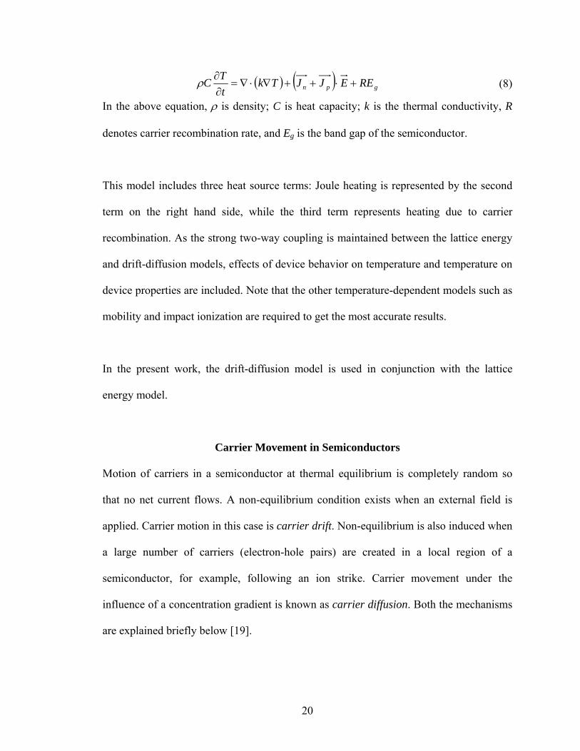
( ) ( ) gpn REEJJTktTC +⋅++∇⋅∇=∂∂ρ (8)
In the above equation, ρ is density; C is heat capacity; k is the thermal conductivity, R
denotes carrier recombination rate, and Eg is the band gap of the semiconductor.
This model includes three heat source terms: Joule heating is represented by the second
term on the right hand side, while the third term represents heating due to carrier
recombination. As the strong two-way coupling is maintained between the lattice energy
and drift-diffusion models, effects of device behavior on temperature and temperature on
device properties are included. Note that the other temperature-dependent models such as
mobility and impact ionization are required to get the most accurate results.
In the present work, the drift-diffusion model is used in conjunction with the lattice
energy model.
Carrier Movement in Semiconductors
Motion of carriers in a semiconductor at thermal equilibrium is completely random so
that no net current flows. A non-equilibrium condition exists when an external field is
applied. Carrier motion in this case is carrier drift. Non-equilibrium is also induced when
a large number of carriers (electron-hole pairs) are created in a local region of a
semiconductor, for example, following an ion strike. Carrier movement under the
influence of a concentration gradient is known as carrier diffusion. Both the mechanisms
are explained briefly below [19].
21
Carrier Drift
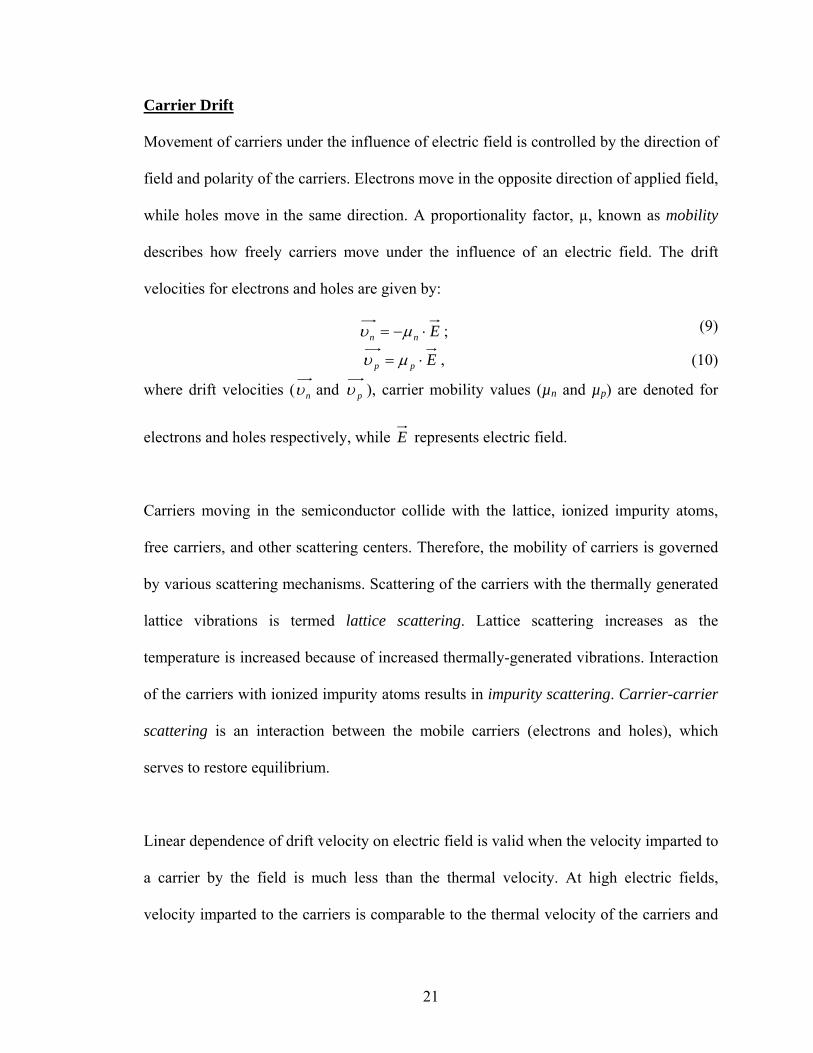
Movement of carriers under the influence of electric field is controlled by the direction of
field and polarity of the carriers. Electrons move in the opposite direction of applied field,
while holes move in the same direction. A proportionality factor, µ, known as mobility
describes how freely carriers move under the influence of an electric field. The drift
velocities for electrons and holes are given by:
Enn ⋅−= µυ ; (9)
Epp ⋅= µυ , (10)
where drift velocities ( nυ and pυ ), carrier mobility values (µn and µp) are denoted for
electrons and holes respectively, while E represents electric field.
Carriers moving in the semiconductor collide with the lattice, ionized impurity atoms,
free carriers, and other scattering centers. Therefore, the mobility of carriers is governed
by various scattering mechanisms. Scattering of the carriers with the thermally generated
lattice vibrations is termed lattice scattering. Lattice scattering increases as the
temperature is increased because of increased thermally-generated vibrations. Interaction
of the carriers with ionized impurity atoms results in impurity scattering. Carrier-carrier
scattering is an interaction between the mobile carriers (electrons and holes), which
serves to restore equilibrium.
Linear dependence of drift velocity on electric field is valid when the velocity imparted to
a carrier by the field is much less than the thermal velocity. At high electric fields,
velocity imparted to the carriers is comparable to the thermal velocity of the carriers and

22
the above assumption is invalid. The drift velocity saturates at high electric fields and is
called the saturation velocity, vsat. At 300 K, the saturation velocity for electrons is 1.07 ×
107 cm/s and for holes is 8.34 × 106 cm/s [21]. The saturation velocity decreases with an
increase in temperature.
Temperature-dependent mobility
Scattering mechanisms that affect the carrier mobility have varying temperature
dependencies. Impurity scattering becomes less effective at high temperature because
high velocity carriers interact less effectively with impurity atoms. The lattice scattering
becomes dominant at high temperature due to the increased lattice vibrations that scatter
the carriers. Thus, mobility increases at low temperatures where the impurity scattering is
dominant, while it decreases at high temperatures where the lattice scattering is dominant.
The drift current densities for electrons and holes are given as:
EnqJ ndriftn µ=, (11)
EpqJ pdriftp µ=, . (12)
Carrier Diffusion
Spatial variation of carrier densities in a semiconductor gives rise to diffusion current.
The diffusion current densities of electrons and holes are calculated by the following
equations:
dxdnqDJ ndiffusionn =, (13)
dxdpqDJ pdiffusionp −=, (14)
23
In the above equations, Dn represents the diffusion constant for electrons and Dp
represents the diffusion constant for holes. The diffusion constant describes carrier
diffusion, while mobility characterizes carrier drift in semiconductors. These two
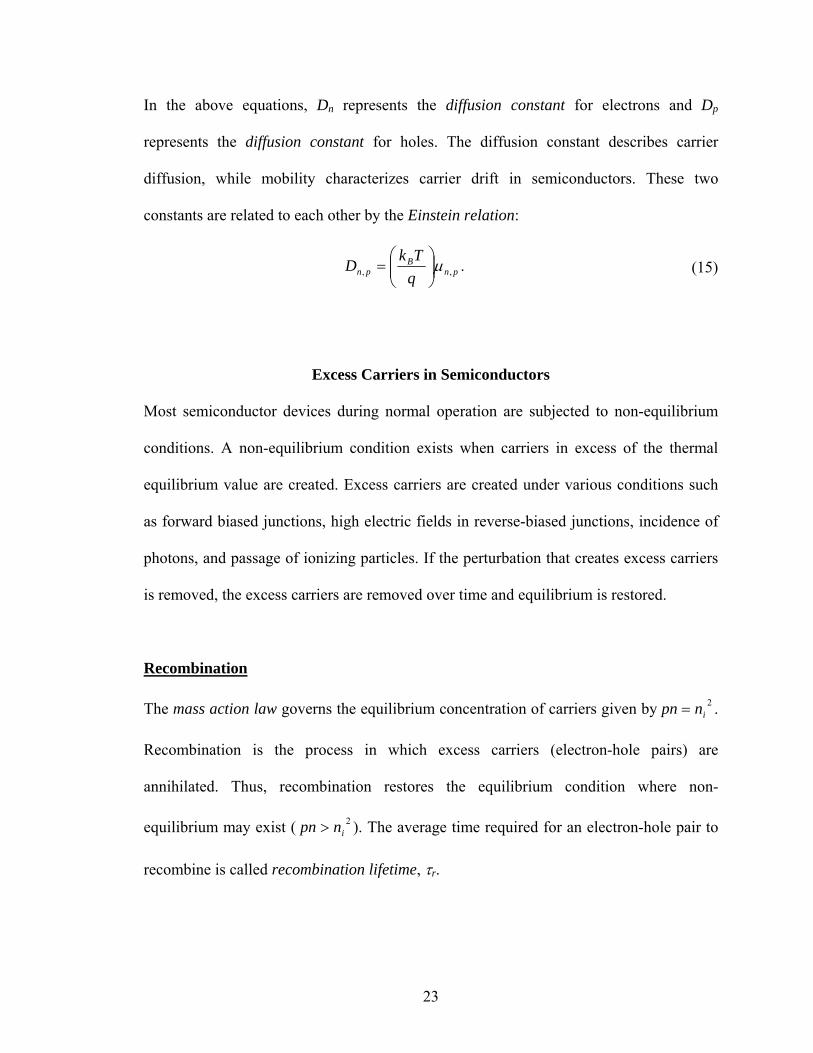
constants are related to each other by the Einstein relation:
pnB
pn qTkD ,, µ⎟⎟⎠
⎞⎜⎜⎝
⎛= . (15)
Excess Carriers in Semiconductors
Most semiconductor devices during normal operation are subjected to non-equilibrium
conditions. A non-equilibrium condition exists when carriers in excess of the thermal
equilibrium value are created. Excess carriers are created under various conditions such
as forward biased junctions, high electric fields in reverse-biased junctions, incidence of
photons, and passage of ionizing particles. If the perturbation that creates excess carriers
is removed, the excess carriers are removed over time and equilibrium is restored.
Recombination
The mass action law governs the equilibrium concentration of carriers given by 2inpn = .
Recombination is the process in which excess carriers (electron-hole pairs) are
annihilated. Thus, recombination restores the equilibrium condition where non-
equilibrium may exist ( 2inpn > ). The average time required for an electron-hole pair to
recombine is called recombination lifetime, τr.
24
Recombination mechanisms that are dominant in semiconductors are classified as band-
to-band recombination (direct recombination), trap-assisted recombination (indirect
recombination), and Auger recombination. The direct recombination is dominant in direct
band gap semiconductors such as GaAs, but unlikely in indirect band gap semiconductors
such as Si. The recombination occurs in the bulk as well as at the surface.
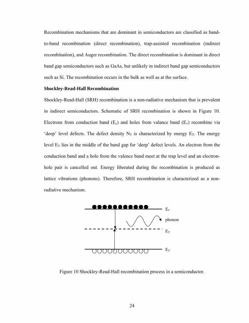
Shockley-Read-Hall Recombination
Shockley-Read-Hall (SRH) recombination is a non-radiative mechanism that is prevalent
in indirect semiconductors. Schematic of SRH recombination is shown in Figure 10.
Electrons from conduction band (Ec) and holes from valance band (Ev) recombine via
‘deep’ level defects. The defect density NT is characterized by energy ET. The energy
level ET lies in the middle of the band gap for ‘deep’ defect levels. An electron from the
conduction band and a hole from the valence band meet at the trap level and an electron-
hole pair is cancelled out. Energy liberated during the recombination is produced as
lattice vibrations (phonons). Therefore, SRH recombination is characterized as a non-
radiative mechanism.
Figure 10 Shockley-Read-Hall recombination process in a semiconductor.
EC
EV
ET
phonon

25
SRH recombination is measured by the recombination rate RSRH, i.e., the number of
electron-hole pairs recombined per unit volume per unit time. The recombination rate
RSRH is given by:
( ) ( )11
2
ppnnnnp
Rnp
ieSRH +++
−=
ττ, (16)
( ) TkEEie
BiTenn /1
−= ; ( ) TkEEie
BTienp /1
−= ,
where n, p are total carrier densities, i.e., the sum of the equilibrium and excess carrier
densities, τp, τn are the recombination lifetimes for holes and electrons, nie denotes
effective intrinsic carrier concentration that accounts for temperature dependence, Ei
denotes intrinsic energy level and ET is trap energy level.
Auger Recombination
Auger recombination involves the interaction of three particles, i.e., two electrons and a
hole or two holes and an electron. When an electron in the conduction band recombines
with a hole in the valence band, the released energy is absorbed by another carrier and the
momentum in this process is also conserved. The energy and momentum is gained by an
electron in n-type semiconductors and a hole in p-type semiconductor. Figure 11 depicts
Auger recombination in n-type semiconductors. This is also a non-radiative
recombination process. Auger recombination is significant in high injection conditions
and regions of high doping concentrations (carrier concentrations > 1019 cm-3). Therefore
it is important in power diodes as the regions near the contacts are heavily doped.
Auger recombination rate RAuger is given by:
( )( )2ie
Augerp
AugernAuger npnpCnCR −⋅+⋅= , (17)
where at 300 K, CnAuger = 2.8 × 10⁻³¹ cm6/s and Cp
Auger = 9.9 × 10⁻³² cm6/s [22].

26
Figure 11 Auger recombination process in a semiconductor.
Temperature-dependence of Intrinsic Carrier Concentration
The intrinsic carrier concentration (ni) is a strong function of the temperature:
,exp2⎟⎟⎠
⎞⎜⎜⎝
⎛ −=
TkE
NNnB
gVCi . (18)
In the above equation, NC and NV are the effective densities of states at the conduction-
band and valence-band edges, respectively. The intrinsic carrier concentration has
exponential temperature dependence, which is very important. The effective densities of
states and band gap are weak functions of temperature.
In extrinsic semiconductors, the carrier concentration is controlled by the impurity
concentration because the intrinsic carrier concentration is much less than the majority
carrier concentration (ni <<n in n-type and ni <<p in p-type semiconductors). However, if
the temperature rise is sufficient, the intrinsic carrier concentration can be comparable to
the impurity concentration. If the intrinsic carrier concentration is comparable to or
greater than the impurity concentration in an extrinsic semiconductor, then the
EC
EV
27
temperature, instead of impurity concentration, controls the carrier concentration in
extrinsic semiconductors.
The power diode structure used in the present work has the base doping level of 3.2 ×
1013 cm-3. The analytical calculation predicts that the intrinsic carrier concentration
around 440 K is comparable to the base doping concentration. The temperature where the
intrinsic concentration approaches the doping level will be called the intrinsic
temperature.
Generation
Generation of carriers in a device leads to non-equilibrium conditions. Carrier generation
is attributed to various mechanisms such as impact ionization, photon absorption, and
passage of fast charged particles through a device. Carrier generation due to impact
ionization and ion strikes is explained in depth because these are the modes of carrier
generation in the present power diode study.
Impact Ionization
Reverse biased pn junctions are subjected to high electric fields because the applied
voltage drop occurs completely within the depletion region. The electric field increases as
the reverse bias on a junction is increased. Free carriers within the depletion region are
accelerated under the influence of high electric fields (above 1 × 10⁵ V/cm). Thus, the
carriers gain high kinetic energies and attain high velocities (~1 × 107 cm/s). When a high
energy carrier collides with the lattice, it can cause an electron from the valence band to
be transferred to the conduction band, creating an electron-hole pair. The ionization
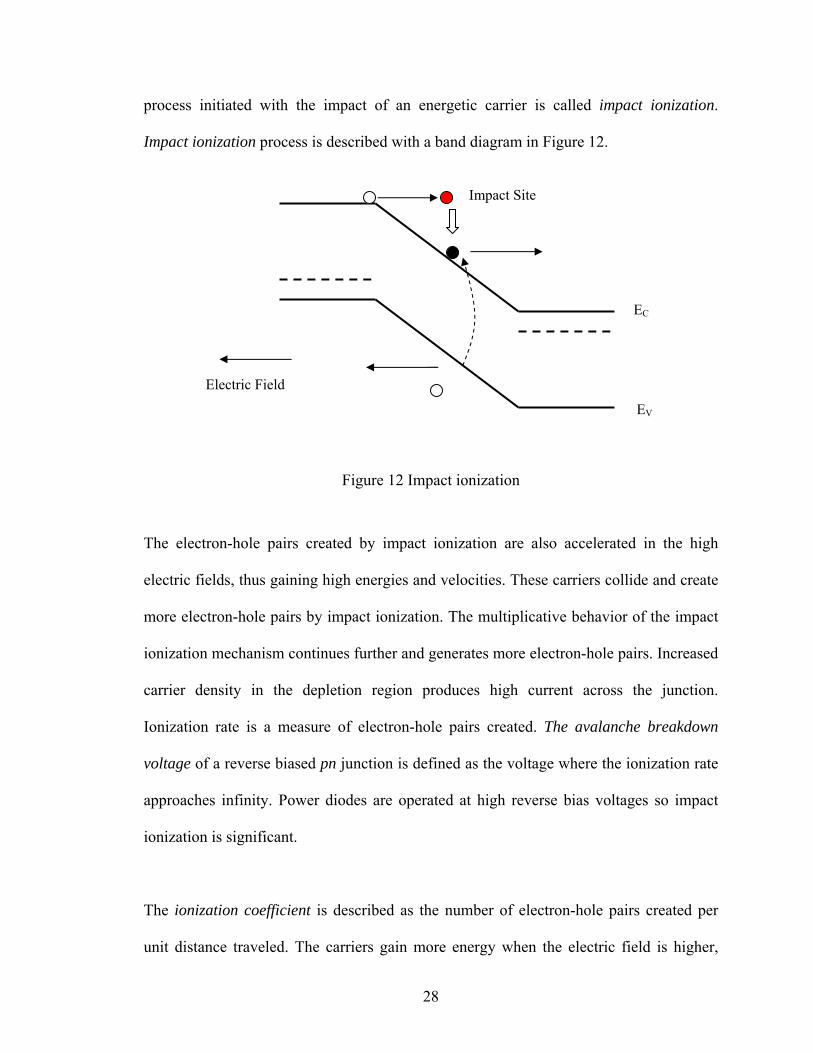
28
process initiated with the impact of an energetic carrier is called impact ionization.
Impact ionization process is described with a band diagram in Figure 12.
Figure 12 Impact ionization
The electron-hole pairs created by impact ionization are also accelerated in the high
electric fields, thus gaining high energies and velocities. These carriers collide and create
more electron-hole pairs by impact ionization. The multiplicative behavior of the impact
ionization mechanism continues further and generates more electron-hole pairs. Increased
carrier density in the depletion region produces high current across the junction.
Ionization rate is a measure of electron-hole pairs created. The avalanche breakdown
voltage of a reverse biased pn junction is defined as the voltage where the ionization rate
approaches infinity. Power diodes are operated at high reverse bias voltages so impact
ionization is significant.
The ionization coefficient is described as the number of electron-hole pairs created per
unit distance traveled. The carriers gain more energy when the electric field is higher,
EC
EV
Electric Field
Impact Site
29
thus ionization rate is a function of electric field and position. The ionization coefficient
is at a maximum where the peak electric field occurs. The electric field dependence of
ionization coefficient for silicon is given by
pnii
icrit
iii JE
JEE
,,
exp)(=
∞
⎥⎥⎦
⎤
⎢⎢⎣
⎡
⎟⎟⎠
⎞⎜⎜⎝
⎛
⋅
⋅−= αα , (19)
where Eicrit is critical electric field for impact ionization and αi
∞ is ionization constant.
Values of the constants for electrons and holes are: Encrit = 1.75 × 10⁶ V/cm, αn
∞ = 3.8 ×
106 cm-1, Epcrit = 3.26 × 10⁶ V/cm and αp
∞ = 2.25 × 107 cm-1.
The carrier generation rate G denotes the number of carriers generated per unit volume
per unit time. The carrier generation due to impact ionization is expressed as
ppnnppnn pnJJG υαυααα +=+= , (20)where Jn and Jp are the current density for electrons and holes, respectively. The current
density can be specified in terms of carrier velocities (υn and υp) and carrier densities (n
and p). The ionization coefficients for electrons and holes (αn and αp) are described
earlier.
Ion strike induced carriers
An energetic ionizing particle passing through materials deposits energy along its path.
Linear energy transfer (LET) describes the energy deposited by the particle per unit
length traveled in the target material. LET is target material-dependent and is usually
described in MeV-cm2/mg. Ionization energy, the energy required to create an electron-
hole pair, for a semiconductor is a characteristic property. For silicon, an average of 3.6
eV is required to create an electron-hole pair [23]. When the energy deposited by a
particle in a semiconductor exceeds the ionization energy, electron-hole pairs are created

30
along its path. The number of created electron-hole pairs is calculated based on the
deposited energy and ionization energy for the material.
In the ion-strike model, generated carriers are deposited uniformly in a cylindrical
column of a specified radius. The overall carrier generation term due to an ion strike is
calculated as:
)(),(),,( tgrlftrlG ⋅= (21)The first term on the right side is the spatial term, while the second term is the temporal
term. The LET is included in the spatial term. Introduction of strike-induced carriers is
modeled as Gaussian in time. Although the normal transit time of an ion through a device
is in the range of femtoseconds, the distribution of induced carriers in the picoseconds
regime is used for simulation stability without the loss of long term accuracy.

31
CHAPTER IV
SIMULATIONS AND RESULTS
Device-level simulations were performed in the present study of single-event burnout in
power diodes and comparisons were made to measurements in the literature. Voss et al.
experimentally observed single-event burnout in power diodes for high energy C12 ions
[13]. A diode that failed due to normal incidence of C12 ion possessing 252 MeV energy
was selected to study the burnout mechanism in power diodes. CFD-Semi-Device
simulations tools developed by CFD Research Corporation were used for the present
work.
3-D simulations require significantly more computation power compared to 2-D
simulations. In this work, a 2-D diode rectangular structure was used for simulations. Not
all device details necessary for modeling the diode are reported in the literature. The
device geometry and breakdown voltage of the diode are reported, but doping
concentrations are not specified. Therefore, approximations were made for features such
as doping profiles in the simulated diode structure.
Diode Structure
A 2-dimensional p+-n--n+ diode structure was created with p+-region width of 100 µm, n-
- region (base) width of 450 µm, and n+-region width of 25 µm [13]. The breakdown
voltage of the diode was specified as 4500 V. Because the base-region doping

32
concentration primarily governs breakdown characteristics of diode, a base-region doping
concentration of 3.2 × 1013 cm-3 was determined for the breakdown voltage of 4500 V.
The doping concentrations of p+- and n+- regions modify the forward-bias characteristics
of the diode, but not the breakdown voltage. As diode burnout is observed during reverse-
bias operation, the p+- and n+- region doping concentration approximations are valid and
do not affect the burnout mechanism. p+- and n+- region doping concentrations were set
as 1 × 1019 cm-3. An abrupt doping profile was used at the p+-n- junction, while a
Gaussian profile was used at the n--n+ junction to avoid sharp potential drop. The
simulated diode structure is shown in Figure 13.
Figure 13 Simulated diode structure showing doping
Device Implementation and Simulation Methodology
CFD-GEOM, the structure modeling and mesh generation tool, was used to create a 2-D
diode model of required dimensions. A structured discretization technique was employed
to divide the diode structure into finite elements for computations. A total of 28000 nodes

33
with a non-uniform distribution were created inside the diode. Very small elements are
required in the regions where large gradients are anticipated. Thus, a very fine mesh was
generated near the pn junction and along the ion track through the diode where high
doping and electric field gradients are expected. The discretized structure is shown in
Figure 14. It is important to discretize the structure into elements that produce a fully
converged solution. Convergence was confirmed by refining the mesh until computed
quantities no longer changed with this mesh. Doping profiles for the structure are
specified in a text format. Doping concentration and roll-off distances along two
coordinate axes for each region are defined in the doping file format.
Figure 14 Diode structure showing refined mesh near junctions and along ion path.
CFD-ACE+ is a graphical user interface that is used to set-up device models and specify
solution parameters. CFD-Semi-Device and Heat modules are selected for all
semiconductor device simulations. The drift-diffusion model is employed in the present
work. The impact ionization model, which is critical in power device simulations, is
Ion path

34
selected because large electric field gradients are encountered. In a few simulations in the
present work, the impact ionization model was excluded to isolate the effect of
avalanche-generated charge. The ion strike model is included in all transient simulations,
where effects of ion strike are simulated. Ion strike parameters such as angle of incidence,
strike-induced track radius, Linear Energy Transfer (LET) are specified in this model. All
of the simulated ion strikes were at normal incidence. The electron-hole pair creation
energy in Si is 3.6 eV/e-h pair, which is used to convert energy to charge density.
Newton’s fully coupled iterative algorithm is utilized to obtain direct solutions to all
semiconductor equations.
The LICE mobility model that includes effects of lattice, impurity, carrier-carrier
scattering along with field-dependent mobility is employed. A constant carrier lifetime of
10 µsec is used for electrons and holes. The thermal conductivity of silicon is 1.5 W/cm-
K and the specific heat is 0.7 J/g-K [24]. The electrical and thermal boundary conditions
for diode simulations are shown in Figure 15. Ohmic contacts to the p+ and n+ regions
assure zero potential drop across them. For all the simulations, the temperatures at
external boundaries were fixed at 300 K unless otherwise specified. Carrier and heat flow
across the symmetry boundary (strike location) is zero, where the axis of symmetry is a
zero flux boundary.

35
Figure 15 Diode structure showing boundary conditions. Symmetry condition indicates no carrier and heat flow across the boundary.
Isothermal simulations (thermal model OFF) assume a default uniform temperature of
300 K inside the device. The values of all temperature-dependent parameters at 300 K are
used in these simulations. Isothermal simulations at different temperature can be
performed by specifying the temperature at all isothermal boundaries. Temperature-
dependent parameters at the specified temperature are used in each specific simulation. In
non-isothermal simulations (thermal model ON), the lattice heat equation calculates
localized temperatures that are used to determine locally temperature-dependent
parameters. As the drift-diffusion equation is solved self-consistently with the lattice heat
equation, localized temperature effects are reflected in device characteristics.
Symmetry
Insulator, isothermal
Ohm
ic, i
soth
erm
al O
hmic, isotherm
al
Strike
36
Steady-state Simulations
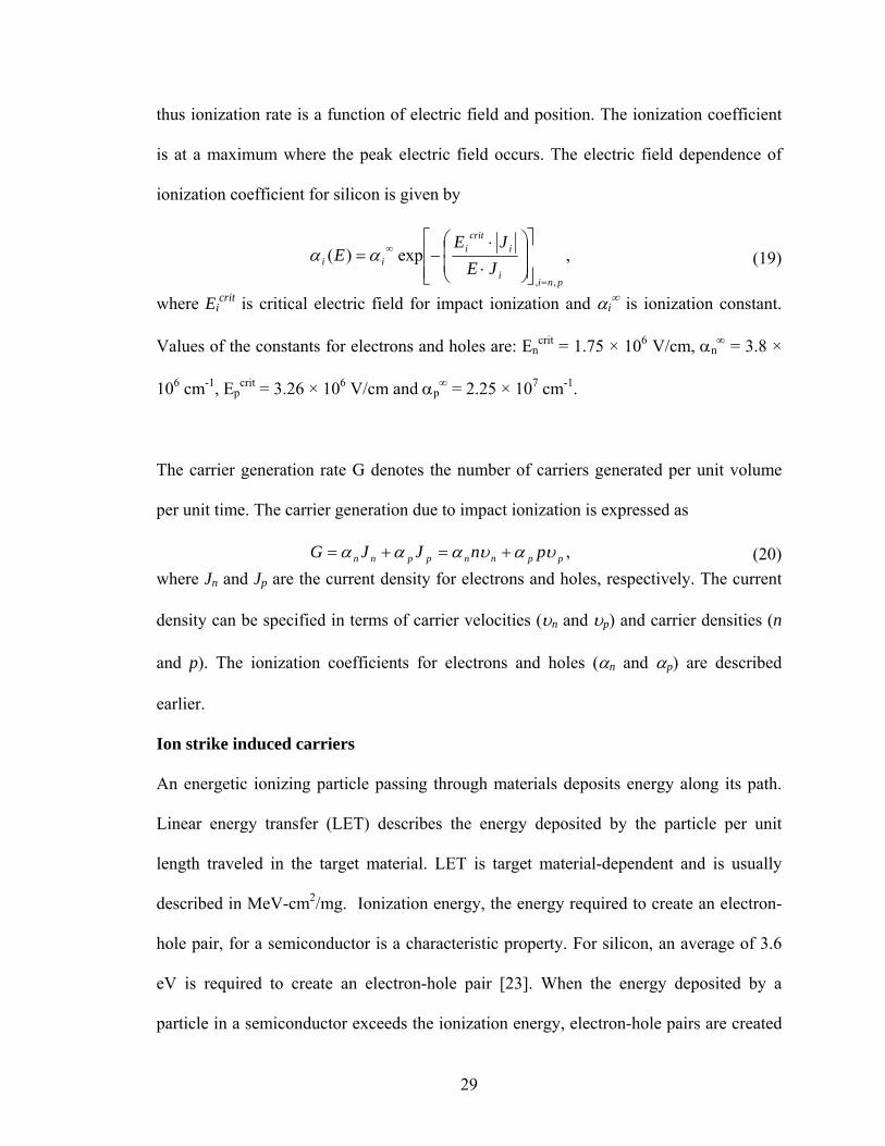
The I-V characteristics of the diode were obtained from steady-state simulations. These
characteristics were simulated using the drift-diffusion model combined with lattice heat
equation. The potential drop across the p+-n- junction can be calculated analytically.
Potential drop across only the p+-n- junction in the simulated structure is acquired by
plotting potential inside the diode at different locations, which is shown in Figure 16. The
potential drop across the p+-n- junction (0.72 V) obtained from the simulated structure is
in agreement with analytically calculated voltage drop (0.74 V).
Figure 16 Built-in potential across the diode at equilibrium.
37
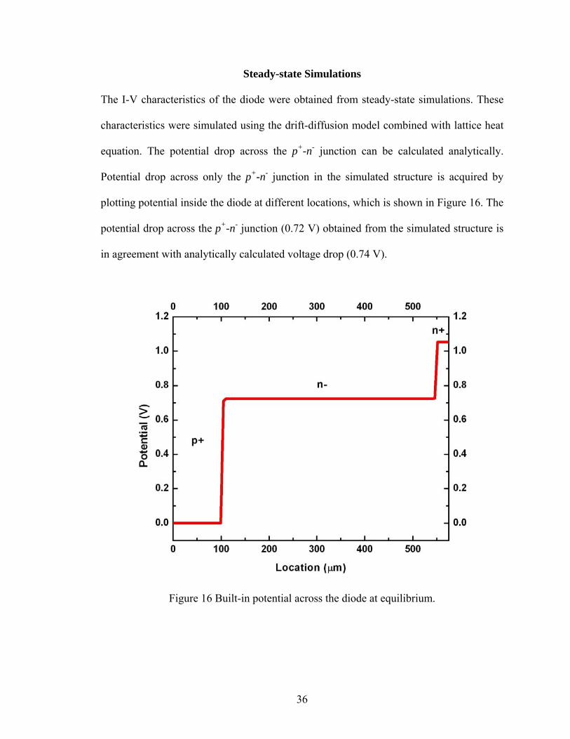
Reverse-bias characteristics were obtained when the bias on the p+ contact was decreased
from 0 V to - 5000 V in steps while the n+ contact was grounded. Impact ionization was
included in the simulation. Figure 17 shows the reverse bias characteristics of the diode.
Simulated breakdown voltage (- 4500 V) is in relatively good agreement with the
analytically calculated breakdown voltage (-4850 V). The maximum electric field at
breakdown (Emax) of 2.096 × 10⁵ V/cm attained in the simulated structure agrees well
with the analytical maximum field of 2.18 × 10⁵ V/cm. The basic diode parameters
obtained for the simulated structure are in agreement with the analytically obtained
parameter values. This confirms that the diode structure is modeled accurately.
Figure 17 Simulated reverse bias characteristics for the power diode structure
38
Transient Simulations
Single-event burnout is a transient process. Current flowing through the diode following
the strike was simulated as a function of time. All ion-strike simulations performed
hereafter involve current flowing through the diode following the strike.
The single-event burnout simulations described here are conducted for a C12 ion
possessing energy of 252 MeV. SRIM [25] simulations were used to calculate the ion
range. The energy loss per unit length along its path does not vary significantly.
Therefore the assumption of uniform carrier density along the ion path is valid. The linear
energy transfer of a 252 MeV C12 ion is estimated as 0.71 MeV-cm2/mg [26]. The charge
filament is formed as a cylindrical column of uniform density. The radial distribution of
generated charge is approximated as a step function and the ion is assumed to pass all the
way through the device. The distribution of radial energy around the track in silicon is
reported by Fageeha et al. for C12 ions with energies of 15 MeV and 100 MeV [27].
Charge density inside the ion-track in the diode is estimated for 252 MeV C12 ions from
the radial dose distribution function. The same charge density is simulated inside the
cylindrical column. With such approximations, an ion track of 0.15 µm radius is modeled
for the chosen ion.
An ion strike is inherently 3D in nature. For symmetric structures, the 3D nature of the
ion-strike can be simulated with 2D axi-symmetric simulations. In the present work, 2D
rectangular simulations are performed due to limitations of the simulation tools.
However, 2D rectangular simulations are capable of capturing physical mechanisms
39
qualitatively. 2D axi-symmetric simulations simulate a cylindrical diode, while 2D
rectangular simulations simulate rectangular parallelepiped diodes. Carrier density inside
the track for a given LET value is determined assuming cylindrical track structure of
specified radius. The ion track in 2-D rectangular coordinate simulations is represented
by a sheet of charge, where the track diameter is the thickness of the charge sheet. The
same carrier density is maintained in the charge sheet in 2-D simulations. Schematic of
the track structure in 2-D simulations is shown in Figure 18. Note that the problem is
symmetric about the plane as shown in Figure 18. The diode is simulated only above the
plane of symmetry, with the ion-strike along the plane of symmetry. This reduced
dimensionality is utilized for computational simplicity. For 2D rectangular simulations,
the depth of the device in the third dimension is considered to be 1 cm. There are no
gradients along the depth of diode. Therefore current is always reported per centimeter
for 2D rectangular simulations.
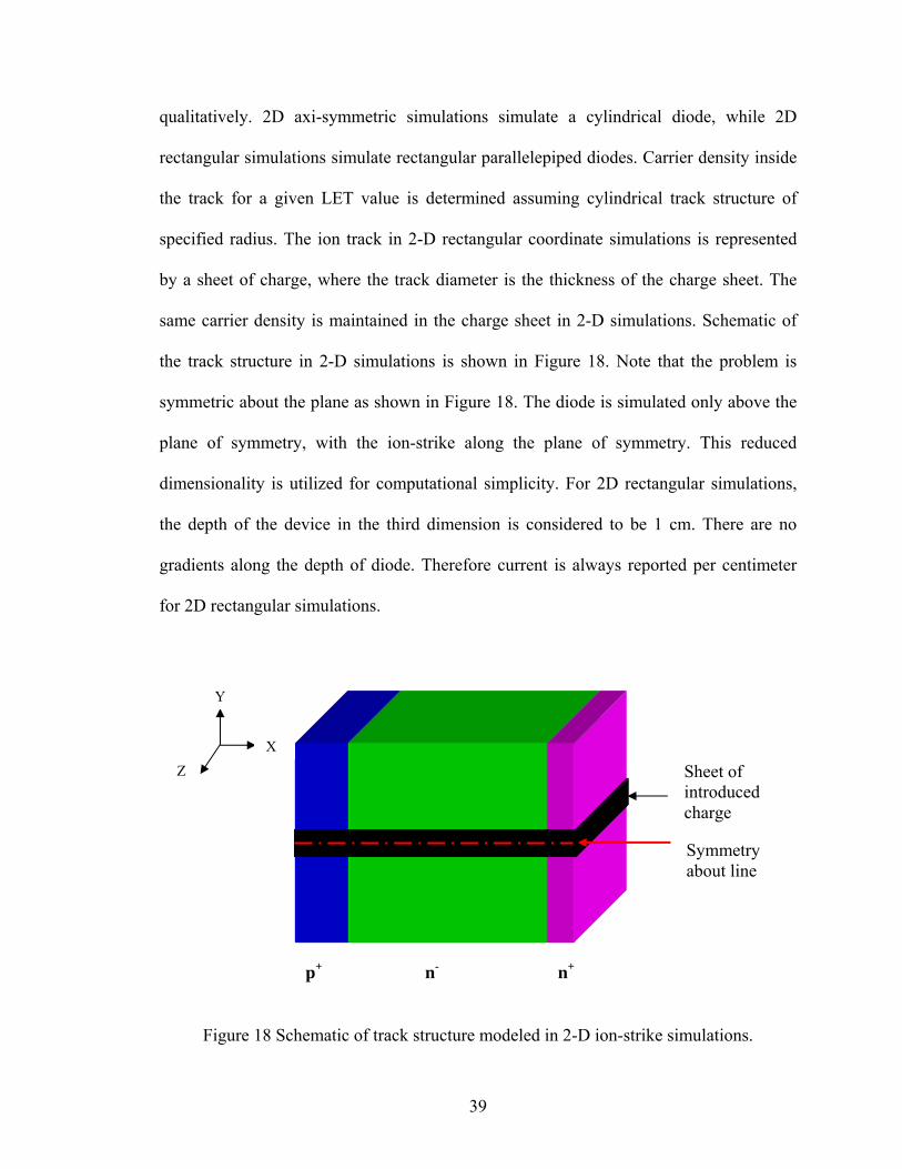
Figure 18 Schematic of track structure modeled in 2-D ion-strike simulations.
p+ n- n+
Sheet of introduced charge
Symmetry about line
X
Z
Y
40
The charge is deposited at the center of the cylindrical diode along its length. The
diffusion of the charge deposited during the ion strike is isotropic in nature. The charge
diffusion is identical in all radial directions. In the case of the 2D rectangular structure,
the charge sheet is introduced along the x-z plane. The gradients due to charge diffusion
are solely along the y-coordinate and not along the depth of the diode (z-coordinate).
Effect of an ion strike on diode current
Single-event burnout is observed only in reverse-biased diodes. The reverse-biased diode
does not conduct current prior to the ion strike, except for the reverse leakage current.
When an ion strikes a diode, the deposited energy generates electron-hole pairs in the
diode. These charges diffuse in the device with time and also drift due to the electric
field. This produces current in the device. Therefore, the reverse-biased diode conducts
current following the ion strike. Current flowing through the diode after the strike is
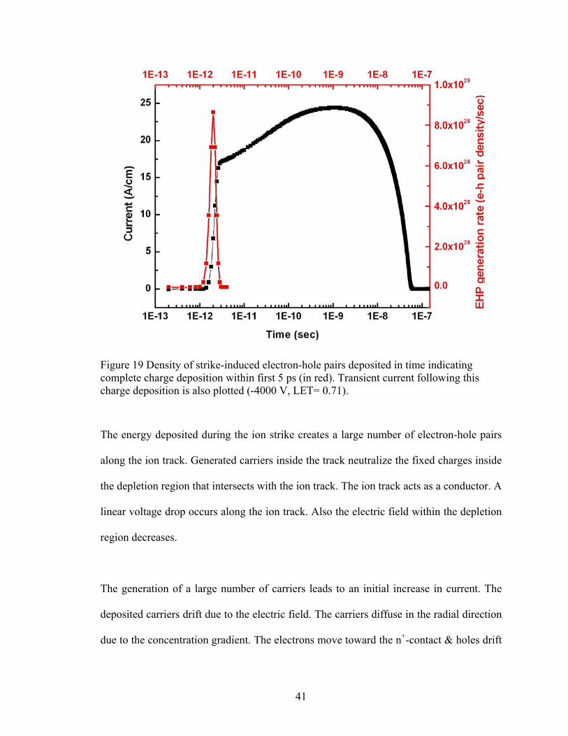
shown in Figure 19. Note that the Gaussian profile of the introduced charge shown in
Figure 19 peaks at 2 ps with a standard deviation of 0.3 ps. The entire charge is deposited
within first 5 ps.
41
Figure 19 Density of strike-induced electron-hole pairs deposited in time indicating complete charge deposition within first 5 ps (in red). Transient current following this charge deposition is also plotted (-4000 V, LET= 0.71).
The energy deposited during the ion strike creates a large number of electron-hole pairs
along the ion track. Generated carriers inside the track neutralize the fixed charges inside
the depletion region that intersects with the ion track. The ion track acts as a conductor. A
linear voltage drop occurs along the ion track. Also the electric field within the depletion
region decreases.
The generation of a large number of carriers leads to an initial increase in current. The
deposited carriers drift due to the electric field. The carriers diffuse in the radial direction
due to the concentration gradient. The electrons move toward the n+-contact & holes drift
42
toward the p+-contact. Therefore, the current increases at short times as the carriers begin
to separate and drift toward the contacts. However, at the end of the ion track, the carrier
density decreases as the carriers move out of the device, allowing the field to increase
locally. The increasing electric field eventually approaches the critical field for impact
ionization. This initiates impact ionization near the high field area. The generation of
carriers due to impact ionization results in increased charge, producing the secondary rise
in current.
At long times, if most of the carriers in the track have diffused away or drifted out of the
device without further addition of carriers, the current decreases. In most situations, the
current eventually falls back to zero and the diode reaches its steady-state condition.
Role of impact ionization model in ion strike simulations
Impact ionization is a very important mechanism that generates additional electron-hole
pairs in reverse-biased power diodes where high electric field gradients are present. Ion-
strike simulations are performed with and without the impact ionization model to
understand the contribution of avalanche-generated charge to the overall current in the
device.
A current trace simulated with and without impact ionization keeping all the other
parameters same is plotted in Figure 20. An increase in the current flowing through the
diode is observed when the impact ionization model is included. The secondary rise in

43
current mentioned previously is evident from Figure 20. Increase in the current was
expected as avalanche-generated carriers contribute to the total current.
Figure 20 Contribution of avalanche-induced charge on current transients through diode after strike
Total charge collected during the strike can be estimated by integrating the temporal
current profile. Difference in the integrals of two current transients gives the avalanche-
generated charge. Figure 21 shows the temporal profile of current due to the avalanche-
induced charge.

44
Figure 21 Current flowing through the diode only due to avalanche-induced charge.
Figure 22 demonstrates that the initial rise in the current following the passage of an ion
depends on the applied bias. For the same number of ion-induced carriers, the initial
increase in the current is greater for higher applied bias. As the applied bias on the diode
increases, the electric field inside the diode increases. Thus more carriers are removed
from the diode immediately after the strike under the influence of larger electric fields
producing higher currents. The secondary rise in current due to impact ionization is also
higher for larger applied biases. The increase in the impact ionization rate with applied
bias [equation 19] explains the higher secondary current for larger bias. The increase in
secondary current is small as temperature effects are included, which is explained later in
this work.
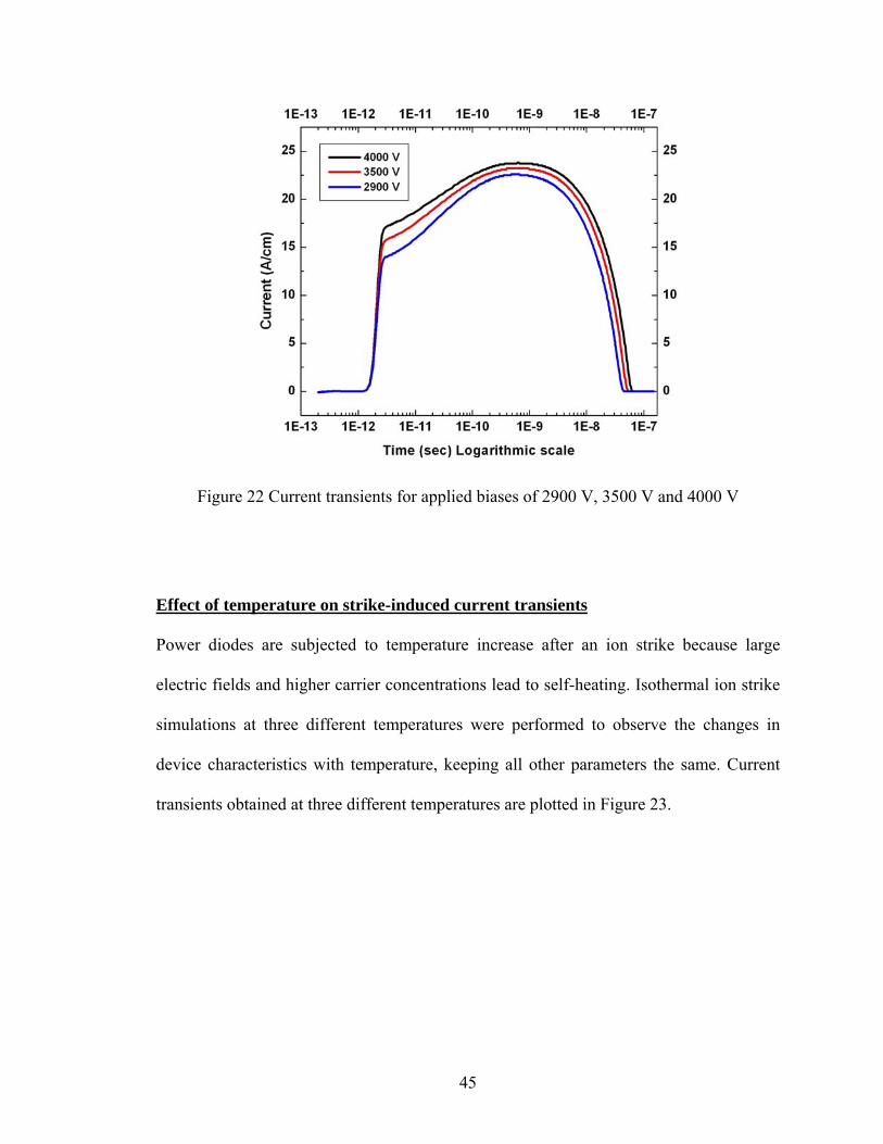
45
Figure 22 Current transients for applied biases of 2900 V, 3500 V and 4000 V
Effect of temperature on strike-induced current transients
Power diodes are subjected to temperature increase after an ion strike because large
electric fields and higher carrier concentrations lead to self-heating. Isothermal ion strike
simulations at three different temperatures were performed to observe the changes in
device characteristics with temperature, keeping all other parameters the same. Current
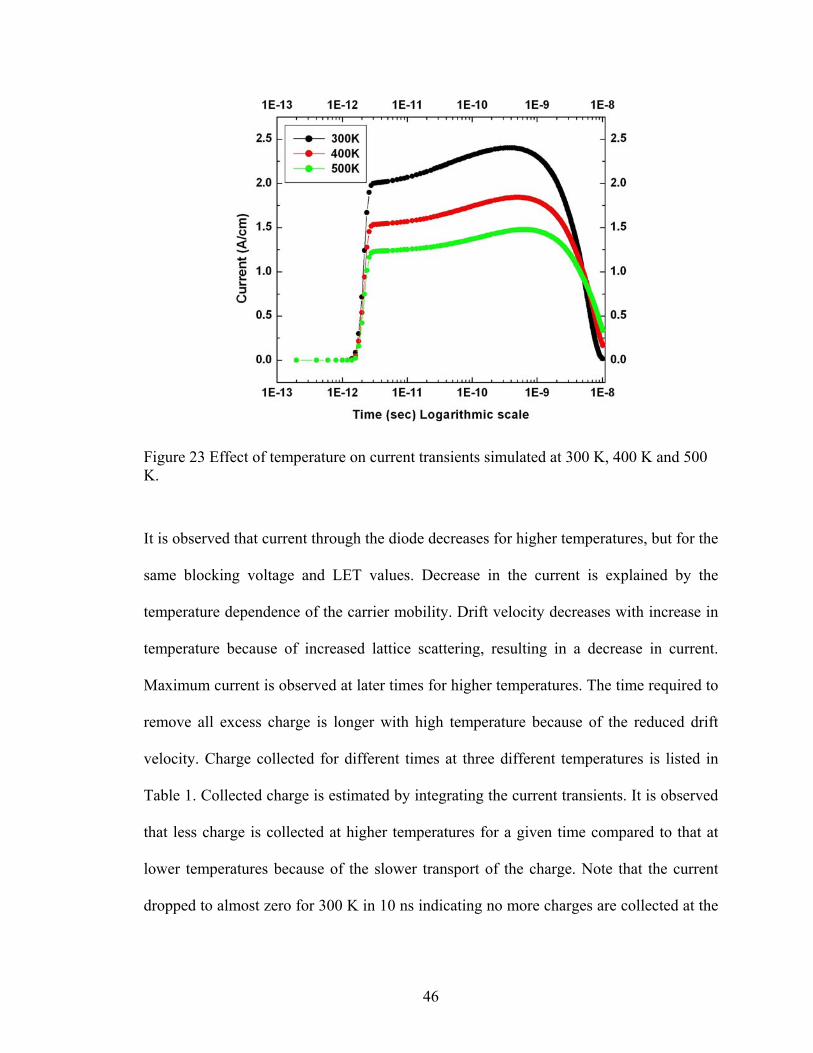
transients obtained at three different temperatures are plotted in Figure 23.
46
Figure 23 Effect of temperature on current transients simulated at 300 K, 400 K and 500 K.
It is observed that current through the diode decreases for higher temperatures, but for the
same blocking voltage and LET values. Decrease in the current is explained by the
temperature dependence of the carrier mobility. Drift velocity decreases with increase in
temperature because of increased lattice scattering, resulting in a decrease in current.
Maximum current is observed at later times for higher temperatures. The time required to
remove all excess charge is longer with high temperature because of the reduced drift
velocity. Charge collected for different times at three different temperatures is listed in
Table 1. Collected charge is estimated by integrating the current transients. It is observed
that less charge is collected at higher temperatures for a given time compared to that at
lower temperatures because of the slower transport of the charge. Note that the current
dropped to almost zero for 300 K in 10 ns indicating no more charges are collected at the
47
contacts. However, for higher temperatures larger current shows that charges are still
being collected at the contacts. This is due to reduced drift velocity at higher temperature.
Table 1 Charge collected in different time after ion strike
Charge collected in time (C/cm) Temperature (K)
10 ps 100 ps 1 ns 10 ns
300 1.6 ×10⁻¹¹ 2.17 ×10⁻¹⁰ 2.35 ×10⁻⁹ 1.09 ×10⁻⁸
400 1.22 ×10⁻¹¹ 1.63 ×10⁻¹⁰ 1.8 ×10⁻⁹ 1.04 ×10⁻⁸
500 9.75 ×10⁻¹² 1.28 ×10⁻¹⁰ 1.44 ×10⁻⁹ 9.53 ×10⁻⁹
Non-isothermal ion strike simulation
Self-heating effects during an ion strike on a diode were simulated when device
temperature was not restricted to a particular temperature. The effect of self heating on
device characteristics was examined. Current transients for the diode biased at 4000 V
with and without self-heating effects are shown in Figure 24. Peak temperature inside the
diode is monitored in time. For the diode biased at 4000 V, the peak temperature
occurred at 32 ns. The temperature distribution inside the diode at 32 ns is shown in
Figure 25. The initial rise in current due to ion-induced charges is the same with inclusion
and exclusion of self-heating effects. Avalanche-induced generation starts when the
electric field increases locally. The localized heating is observed due to large electric
field and current near the intersection of the ion track and the pn junction inside the base
region. A local temperature rise is observed due to self-heating effects. As the local

48
temperature increases, a decrease in current is observed due to reduced carrier mobility.
For the diode biased at 4000 V, avalanche-induced current peaks at 5 ns, while peak
temperature is observed at 32 ns. Even after the avalanche-generated carrier
concentration peaks, the electric field increases as carriers move. Increase in the electric
field in the presence of carriers leads to further self-heating. Intrinsic carrier
concentration also increases with temperature. Increase in the carrier concentration and
decrease in the carrier mobility at higher temperatures are two competing processes.
Maximum temperature is reached when local carrier concentration is reduced
significantly to reduce self-heating and temperature starts to decrease. The temperature
distribution inside the diode at 32 ns shows that the localized high temperature region
extends only 1 µm along radial direction away from the strike. The thermal penetration
depth for transient simulation times of the order of 1.5 × 10⁻⁷ sec is tlth κ= ≈ 3.6 µm,
where κ (0.87 cm2/s) is the thermal diffusivity of silicon. Because the penetration depth is
much smaller than the diode dimensions, the boundary condition does not affect the
thermal response.

49
Figure 24 Comparison of current transients with and without self-heating effects at 4000 V applied bias.
Figure 25 Temperature distribution near pn junction at 32 ns after strike at 4000 V.
50
Self-heating effects were studied as a function of applied bias. Applied bias values of
2900 V, 3500 V, and 4000 V were chosen because single-event burnout was observed
experimentally when the diode was biased higher than 3000 V. Current transients
observed for these three applied biases are compared in Figure 26. Electric field and
electron density along plane of incident ion inside the hot spot are monitored in time and
shown in Figure 27 and Figure 28. The temperature distribution inside the diode was
monitored in time. Peak temperatures observed in the diode are plotted in Figure 29.
Current through the diode was higher for larger applied bias, however it returned to zero
for all three applied biases. Current and temperature inside the diode decrease after the
initial rise suggesting thermal runaway did not occur. Avalanche-generated charge
increases with bias. Thus the results are consistent as more charge was collected for
higher applied biases. Evolution of electric field seen in Figure 27 indicates that
maximum 300 kV/cm electric field was observed within 0.5 µm from interface. However,
inside the hotspot (1-3 µm) maximum electric field was less than 200 kV/cm. Critical
electric field for impact ionization is ~ 1000 kV/cm. Thus electric field inside the diode
was not high enough to generate considerably large number of avalanche-generated
carriers. Secondary current rise, primarily because of avalanche-generated charge, was
not considerably different for lower applied biases. Self-heating is calculated from
product of local current density and electric field. Although difference is not large, higher
peak temperatures were observed due to the higher generation rate for larger biases.
Intrinsic carrier concentration increases with temperature. For the temperatures generated
in these simulations (~ 575 K), intrinsic carrier concentration is ~ 3 × 1015 cm-3. This is
much lower than the deposited carrier density. Therefore intrinsic carrier concentration
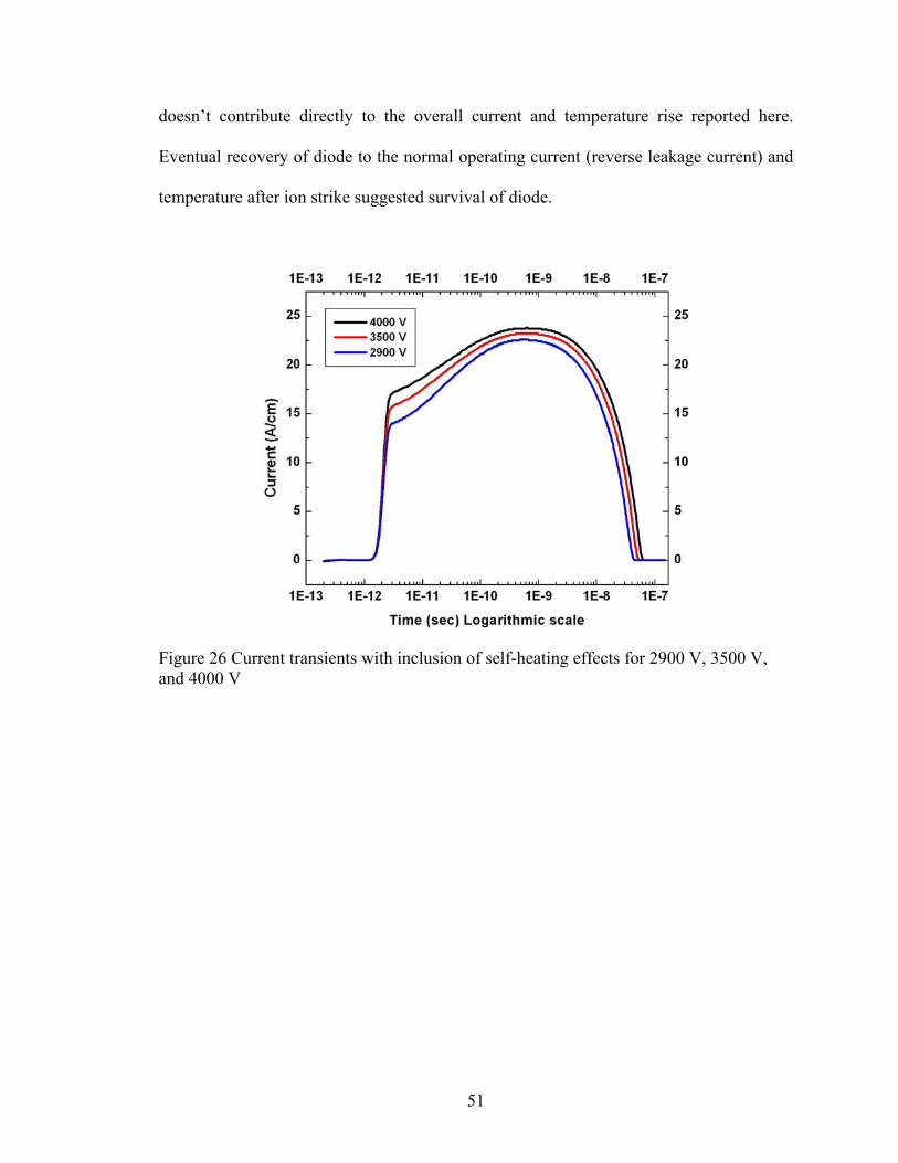
51
doesn’t contribute directly to the overall current and temperature rise reported here.
Eventual recovery of diode to the normal operating current (reverse leakage current) and
temperature after ion strike suggested survival of diode.
Figure 26 Current transients with inclusion of self-heating effects for 2900 V, 3500 V, and 4000 V
52
Figure 27 Electric field at a distance from p+-n- interface inside n- region in the plane of incident ion (4000 V case)
Figure 28 Electron density at a distance from p+-n- interface inside n- region in the plane of incident ion (4000 V case)

53
A higher peak temperature for a larger bias suggests avalanche-induced charge is
responsible for the temperature rise. The short term current rise immediately after the
strike is insignificant because a large number of strike-induced carriers reduce the electric
field. As the carriers near the junctions are being removed, electric field begins to
increase. The temperature rises considerably as avalanche-induced carriers are created.
Also, it is important to note that the temperature peak occurred later in time for higher
applied biases. This indicates that the impact ionization mechanism is the driving force
for self-heating, not the strike-induced charge.
Figure 29 Peak temperatures inside the device at different time after the strike for applied biases of 2900 V, 3500 V and 4000 V. Same plot on linear time scale is shown in the inset.
54
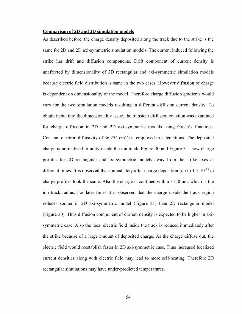
Comparison of 2D and 3D simulation models
As described before, the charge density deposited along the track due to the strike is the
same for 2D and 2D axi-symmetric simulation models. The current induced following the
strike has drift and diffusion components. Drift component of current density is
unaffected by dimensionality of 2D rectangular and axi-symmetric simulation models
because electric field distribution is same in the two cases. However diffusion of charge
is dependent on dimensionality of the model. Therefore charge diffusion gradients would
vary for the two simulation models resulting in different diffusion current density. To
obtain incite into the dimensionality issue, the transient diffusion equation was examined
for charge diffusion in 2D and 2D axi-symmetric models using Green’s functions.
Constant electron diffusivity of 36.254 cm2/s ia employed in calculations. The deposited
charge is normalized to unity inside the ion track. Figure 30 and Figure 31 show charge
profiles for 2D rectangular and axi-symmetric models away from the strike axes at
different times. It is observed that immediately after charge deposition (up to 1 × 10-13 s)
charge profiles look the same. Also the charge is confined within ~150 nm, which is the
ion track radius. For later times it is observed that the charge inside the track region
reduces sooner in 2D axi-symmetric model (Figure 31) than 2D rectangular model
(Figure 30). Thus diffusion component of current density is expected to be higher in axi-
symmetric case. Also the local electric field inside the track is reduced immediately after
the strike because of a large amount of deposited charge. As the charge diffuse out, the
electric field would reestablish faster in 2D axi-symmetric case. Thus increased localized
current densities along with electric field may lead to more self-heating. Therefore 2D
rectangular simulations may have under-predicted temperatures.
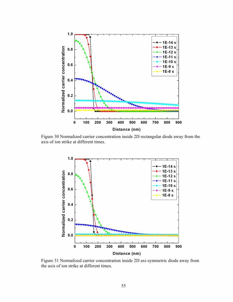
55
Figure 30 Normalized carrier concentration inside 2D rectangular diode away from the axis of ion strike at different times.
Figure 31 Normalized carrier concentration inside 2D axi-symmetric diode away from the axis of ion strike at different times.
56
CHAPTER V
CONCLUSION
The main objective of the present work was to study single-event burnout mechanisms in
power diodes. A 2D rectangular diode structure, similar to a diode structure for which
burnout failure was observed experimentally, was studied with device-based simulations.
Transient ion-strike simulations were performed where the diode current was observed in
time. Ion-strike parameters were chosen based on experimental data. Temperature
dependence was included through coupled electro-thermal models to observe the effects
of internal device temperature on device characteristics and to study burnout mechanism.
Self-heating effects inside the diode were simulated with coupled electro-thermal
simulations. Parameters such as carrier mobility, intrinsic carrier concentration and
impact ionization rate are dependent on temperature. Variation in temperature inside the
diode affects the electrical characteristics of the diode. Simulations predicted lower
current at larger temperatures assuming isothermal conditions. A decrease in the transient
diode current for higher temperatures is attributed to reduced carrier mobility due to
increased lattice scattering. For higher temperatures, current returned to zero later in time
compared to low temperatures because of reduced carier drift velocity. The induced
charge is removed slower for higher temperatures due to reduced carrier drift velocity.
Intrinsic carrier concentration increases for higher temperature because more electrons
have sufficient energy to overcome the bandgap. Impact ionization rate is lower for high

57
temperatures. However, this effect is not included in the above simulations. Thus these
are competing effects when thermal dependence is included.
Avalanche-induced charge has a significant contribution on the transient current through
diode. The observed secondary rise in current is due to the avalanche-generated charge.
Large currents in the presence of large electric fields lead to localized heat generation.
This resulted in a localized increase in diode temperature. Peak temperatures inside the
diode occurred after the peak of avalanche-induced charge was observed. An increase in
temperature is attributed to the avalanche-induced charge that leads to self-heating of the
diode. Avalanche-generated charge is greater for larger applied biases because of high
electric fields. For larger applied biases, peak temperatures inside the diode are higher.
This is a result of higher heat generation rates for larger biases. Again, avalanche-induced
charge is responsible for self-heating.
Intrinsic carrier concentration, which is a function of temperature, increases in a localized
region. Increase in carrier concentration does not contribute to current increase in the
diode and does not lead to further heating because the electric field is reduced. Thus the
diode doesn’t enter into a thermal feedback loop as originally hypothesized [18].
The present device-level simulations including self-heating effects did not identify
thermal feedback as the failure mechanism for power diodes. Working within the
capabilities of simulations tools, based on the assumptions made and parameters chosen,
it was observed that self-heating effects play negligible role in powder diode burnout.
58
However, more accurate simulations need to be performed before complete exclusion of
self-heating effects for burnout studies. The current simulations emphasize the
importance of impact ionization modeling because impact ionization induced charge is
responsible for heating of the diode. Localized heating also affects the total charge
generated.
There are several parameters that can be improved in further studies. The 2D simulations
described here were conducted using rectangular coordinates, which simulate the ion
strike as an infinite sheet of charge, unlike in the true 3D situation. Simple comparison of
charge diffusion in 2D rectangular and 2D axi-symmetric models suggests that 2D
rectangular simulations could have under-predicted temperatures inside the diode after
strike. Thus the temperature profile would be different due to altered heat generation rate
and profile. This will influence electrical characteristics of the diode. Thus further 2D
axi-symmetric and possibly full 3D simulations are necessary. The ion track structure
generated based on the ion energy deposited along its path is required. Temperature-
dependent impact ionization model needs to be included for future studies.
59
REFERENCES
1. Stassinopoulos EG and Raymond JP. The Space Radiation Environment for Electronics. Proceeding of the IEEE 1988; 76(11):1423-42.
2. Fleetwood DM and Winokur PS. Radiation Effects in the Space
Telecommunications Environment. Proceedings of the 22nd International Conference on Microelectronics 2000; 1: 43-9.
3. Zeller HR. Cosmic ray induced failures in high power semiconductor devices.
Solid-State Electronics 1995; 38(12):2041-6.
4. Ziegler J, Lanford W. The effect of sea level cosmic rays on electronic devices. IEEE International Digest of Technical Papers 1980; 23:70-1.
5. Waskiewicz AE, Groninger JW, Strahan VH, Long DM. Burnout of power mos
transistors with heavy ions of 252-Cf. IEEE Transactions on Nuclear Science 1986; 33:1710-3.
6. Roubaud F, Dachs C, Palau JM, Gasiot J, Tastet P. Experimental and 2D
simulation study of of the single-event burnout in n-channel power MOSFET’s. IEEE Transactions on Nuclear Science 1993; 40(6):1952-8.
7. Dachs C, Roubaud F, Palau JM, Bruguier G, Gasiot J. Evidence of the ion’s
impact position effect on seb in n-channel power mosfets. IEEE Transactions on Nuclear Science 1994; 41(6):2167-71.
8. Johnson GH, Schrimpf RD, Galloway KF. Temperature dependence of single-
event burnout in n-channel power MOSFETs. IEEE Transactions on Nuclear Science 1992; 39(6):1605-12.
9. Johnson GH, Hohl JH, Schrimpf RD, Galloway KF. Simulating single-event
burnout of n-channel power MOSFET’s. IEEE Transactions on Electron Devices 1993; 40(5):1001-8.
10. Kabza H, Schulze HJ, Gestenmaier Y, Voss P, Wilhelmi J, Schmid W et al.
Cosmic radiation as a possible cause for power device failure and possible countermeasures. Proceedings of 6th International Symposium on power Semiconductor Devices & IC’s 1994; 9-12.
11. Zeller HR. Cosmic ray induced failures in high power semiconductor devices.
Microelectronics Reliability 1997; 37(10):1711-18.
60
12. Brand H and Selberherr. Two-Dimensional Simulation of Thermal Runaway in a Nonplanar GTO-Thyritor. IEEE Transactions on Electron Devices 1995; 42(12):2137-46.
13. Voss P, Maier KH, Becker HW, Normand E, Wert JL, Oberg DI et al. Irradiation
experiments with high voltage power devices as a possible means to predict failure rates due to cosmic rays. Proceedings of the IEEE International Symposium on power Semiconductor Devices & IC’s 1997; 169-73.
14. Busatto G, Iannuzzo F, Wyss J, Pantano D and Bisello D. Effects of Heavy Ion
Impact on Power Diodes. Radiation and Its Effects on Components and Systems 1999; 205-9.
15. Soelkner G, Voss P, Kaindl W, Wachukta G, Maier KH and Becker HW. Charge
Carrier Avalanche Multiplication in High-Voltage Diodes Triggered by Ionizing Radiation. IEEE Transactions on Nuclear Science 2000; 47(6):2365-72.
16. Kuboyama S, Matsuda S, Kano T, Ishii T. Mechanism for single-event burnout of
power MOSFETs and its characterization technique. IEEE Transactions on Nuclear Science 1992; 39(6):1698-1703.
17. Albadri AM, Schrimpf RD, Walker DG, and Mahajan SV. Coupled electro-
thermal simulations of single event burnout in power diodes. IEEE Transactions on Nuclear Science 2005; 52(6): 2194-2199.
18. Albadri AM, Walker DG, Fisher TS, and Schrimpf RD. Simulation of single
event failure in power diodes. Proc. Int. Mechanical Engineering Congress Expositions, New Orleans, LA 2002; 17-22.
19. Muller RS and Kamins TI. Device electronics for Integrated Circuits. 3rd ed. John
Wiley and Sons; 2003.
20. CFD Research Corporation. CFD-ACE+ User Manual V2003. Huntsville, Alabama 35805, 2003.
21. Caughey DM and Thomas RE. Carrier mobilities in silicon empirically related to
doping and field. Proceedings of IEEE 1967; 55: 2192-2193
22. Dziewior J and Schmid W. Auger coefficients for highly doped and highly excited silicon. Applied Physics Letters 1977; 31:346-348.
23. McKay KG, McAfee. Electron multiplication in Silicon and Germanium. Physical
Review 1953; 91(5):1079-84.
24. Sze SM. Physics of Semiconductor Devices. 2nd ed. John Wiley and Sons; 1981.
25. Biersack JP, Ziegler JF. SRIM Version 2003.26: Pergamon Press, 2003.
61
26. http://tvdg10.phy.bnl.gov/LETCalc.html
27. Fageeha O, Howard J, Block RC. Distribution of radial energy deposition around
the track of energetic charged particles in silicon. Journal of Applied Physics 1994; 75(5):2317-21.
28. Canali C, Majni G, Minder R, and Ottaviani G. Electron and hole drift velocity
measurements in silicon and their empirical relation to electric field and temperature. IEEE Transactions on electron Devices 1975; 11:1045-47.