Control technique for power device electro-thermal stress
6
Control technique for power device electro-thermal stress minimisation in non-linear load variable-frequency resonant power converters F. Carastro * , A. Castellazzi, J. Clare, P. Wheeler Department of Electrical and Electronic Engineering, University of Nottingham, Nottingham NG7 2RD, UK article info Article history: Received 8 July 2010 Accepted 13 July 2010 Available online 7 August 2010 abstract This work proposes the development of a control technique to ensure soft-switching of the active devices in a high-voltage high-frequency power supply, during all operational conditions. The study is carried out with relevance to an industrial electrostatic precipitator system, based on a series-resonant converter topology. The main operational features of the circuit are presented, detailing the requirements for high efficiency and high reliability. Based on theoretical analysis, the development of specific control solutions is thoroughly discussed. Experimental results are presented to demonstrate the validity of the considered approach for maximizing circuit performance and reducing the risk of degradation of the power switches. Ó 2010 Elsevier Ltd. All rights reserved. 1. Introduction In a variety of industrial processes such as gas and oil fired power stations, cement and steel production facilities, waste incineration plants, high power electrostatic precipitators (EPS) are used to remove dust particles and reduce polluting emissions [1]. For most precipitators, a power supply with a high voltage output of 50–100 kV with high short-circuit capability is required to achieve the best efficiency of dust removal. Traditional power supplies in use for high voltage EPS systems are based upon 50/ 60 Hz line frequency technology, which results in quite cumber- some designs [2]. Increasingly stringent environmental policies across the world are causing this market to grow rapidly and broadly. This is pushing research towards novel power supply architectures with improved performance (dynamic response and efficiency), power density and reliability [2,3]. High-fre- quency resonant converter topologies are now being considered to meet these targets. One of the advantages of these topologies is the possibility to switch the active devices with virtually non-dissipative transitions (soft-switching), both at turn-on and turn-off, thus optimizing efficiency and minimising the electro- thermal stress of the devices [4]. However, due to the intrinsically non-linear nature of the load, sophisticated control techniques are required to ensure soft-switching resonant transitions, taking into account that the regulation of the converter output voltage and current require not only pulse-width modulation, but also vari- able frequency of operation. 2. Circuit description and simulation results This paper considers a converter rated at 100 kV, 2 A. Although resonant converter topologies have been established for some time in lower power applications, there are relatively few examples of their deployment in high power applications such as that described here. The power circuit design has been developed to be capable of supporting continuous operation of the EPS. Fig. 1 shows a sche- matic diagram of the converter and its control platform. The sys- tem consists of an input rectifier and a dc-link capacitor, followed by an H-bridge connected to a series resonant tank. A high frequency transformer incorporated into the supply is used to step-up the voltage to 25 kV. A two stage Cockcroft–Walton voltage multiplier is used to step-up the voltage to the nominal 100 kV. The precipitator load, indicated as R L , changes according to the properties and quantity of the dust. When a spark occurs in- side the EPS, this effectively short-circuits the output of the power supply. The power supply must be capable of surviving the effects of this condition and must quickly reduce its current to zero in or- der to extinguish the spark. The short-circuit equivalent load oc- curs on average 50 times per minute. During recovery of the steady state it is paramount to ensure soft-switching of the active devices to ensure good dynamic performance and avoid switch electro-thermal overload, degradation and failure. The full electrical design of the proposed power supply has been carried out assuming that the converter switches in a square wave mode to excite the resonant tank. A load quality factor (Q) of 3 has been selected to achieve approximately sinusoidal tank waveforms without excessively large tank components. In addition to simplify the mathematical model, rectifier, filter and load have been re- placed with an equivalent AC resistance. The expression of the equivalent resistance can be calculated under the assumption of 0026-2714/$ - see front matter Ó 2010 Elsevier Ltd. All rights reserved. doi:10.1016/j.microrel.2010.07.044 * Corresponding author. Tel.: +44 (0) 115 84 6. E-mail address: [email protected] (F. Carastro). Microelectronics Reliability 50 (2010) 1738–1743 Contents lists available at ScienceDirect Microelectronics Reliability journal homepage: www.elsevier.com/locate/microrel
Transcript of Control technique for power device electro-thermal stress

Microelectronics Reliability 50 (2010) 1738–1743
Contents lists available at ScienceDirect
Microelectronics Reliability
journal homepage: www.elsevier .com/locate /microrel
Control technique for power device electro-thermal stress minimisationin non-linear load variable-frequency resonant power converters
F. Carastro *, A. Castellazzi, J. Clare, P. WheelerDepartment of Electrical and Electronic Engineering, University of Nottingham, Nottingham NG7 2RD, UK
a r t i c l e i n f o a b s t r a c t
Article history:Received 8 July 2010Accepted 13 July 2010Available online 7 August 2010
0026-2714/$ - see front matter � 2010 Elsevier Ltd. Adoi:10.1016/j.microrel.2010.07.044
* Corresponding author. Tel.: +44 (0) 115 84 6.E-mail address: [email protected] (
This work proposes the development of a control technique to ensure soft-switching of the active devicesin a high-voltage high-frequency power supply, during all operational conditions. The study is carried outwith relevance to an industrial electrostatic precipitator system, based on a series-resonant convertertopology. The main operational features of the circuit are presented, detailing the requirements for highefficiency and high reliability. Based on theoretical analysis, the development of specific control solutionsis thoroughly discussed. Experimental results are presented to demonstrate the validity of the consideredapproach for maximizing circuit performance and reducing the risk of degradation of the power switches.
� 2010 Elsevier Ltd. All rights reserved.
1. Introduction
In a variety of industrial processes such as gas and oil firedpower stations, cement and steel production facilities, wasteincineration plants, high power electrostatic precipitators (EPS)are used to remove dust particles and reduce polluting emissions[1]. For most precipitators, a power supply with a high voltageoutput of 50–100 kV with high short-circuit capability is requiredto achieve the best efficiency of dust removal. Traditional powersupplies in use for high voltage EPS systems are based upon 50/60 Hz line frequency technology, which results in quite cumber-some designs [2]. Increasingly stringent environmental policiesacross the world are causing this market to grow rapidly andbroadly. This is pushing research towards novel power supplyarchitectures with improved performance (dynamic responseand efficiency), power density and reliability [2,3]. High-fre-quency resonant converter topologies are now being consideredto meet these targets. One of the advantages of these topologiesis the possibility to switch the active devices with virtuallynon-dissipative transitions (soft-switching), both at turn-on andturn-off, thus optimizing efficiency and minimising the electro-thermal stress of the devices [4]. However, due to the intrinsicallynon-linear nature of the load, sophisticated control techniques arerequired to ensure soft-switching resonant transitions, taking intoaccount that the regulation of the converter output voltage andcurrent require not only pulse-width modulation, but also vari-able frequency of operation.
ll rights reserved.
F. Carastro).
2. Circuit description and simulation results
This paper considers a converter rated at 100 kV, 2 A. Althoughresonant converter topologies have been established for some timein lower power applications, there are relatively few examples oftheir deployment in high power applications such as that describedhere. The power circuit design has been developed to be capable ofsupporting continuous operation of the EPS. Fig. 1 shows a sche-matic diagram of the converter and its control platform. The sys-tem consists of an input rectifier and a dc-link capacitor,followed by an H-bridge connected to a series resonant tank. Ahigh frequency transformer incorporated into the supply is usedto step-up the voltage to 25 kV. A two stage Cockcroft–Waltonvoltage multiplier is used to step-up the voltage to the nominal100 kV. The precipitator load, indicated as RL, changes accordingto the properties and quantity of the dust. When a spark occurs in-side the EPS, this effectively short-circuits the output of the powersupply. The power supply must be capable of surviving the effectsof this condition and must quickly reduce its current to zero in or-der to extinguish the spark. The short-circuit equivalent load oc-curs on average 50 times per minute. During recovery of thesteady state it is paramount to ensure soft-switching of the activedevices to ensure good dynamic performance and avoid switchelectro-thermal overload, degradation and failure.
The full electrical design of the proposed power supply has beencarried out assuming that the converter switches in a square wavemode to excite the resonant tank. A load quality factor (Q) of 3 hasbeen selected to achieve approximately sinusoidal tank waveformswithout excessively large tank components. In addition to simplifythe mathematical model, rectifier, filter and load have been re-placed with an equivalent AC resistance. The expression of theequivalent resistance can be calculated under the assumption of

C
Ltank
3-phase Supply
x6
Lf
Cf
RL
Voltage Multiplier
GATE DRIVEVOLTAGE
TRANSDUCER
A/D
Programmable Control Platform
VABVdc
V
I
S1
S2
GATE SIGNALS
PROTECTION AND CONTROL MEASUREMENTS
InputRectifier
Ctank
HVHF_TR
Cstack_1
Cstack_2
Cstack_3
Cstack_4
Itank
S4
A/D
Nonlinear load
A
B
PEAK DETECTOR
CURRENT TRANSDUCER
VOLTAGE
TRANSDUCER
S3
Fig. 1. Schematic of the single-phase power supply and control platform.
Table 1Power supply specifications and design results.
Description Symbol Value
Power supply specificationLoad voltage V 100 kVLoad voltage ripple Vr <3%Load current I 2AOutput power P 200 kWLoad voltage recovery V 1.5 kV/msQuality Factor Q 3Switching frequency fsw 20 kHzDC-link Vdc 600 V
Design resultsTank inductor Ltank 0.027 mHTank capacitor Ctank 2.04 lFNatural frequency f0 21.2 kHzEPS filter inductor Lf 3 mHEPS capacitance Cf 0.5 lFDC-link capacitor C 7 mFTransformer turn ratio N 1:47Voltage multiplier gain km 4
F. Carastro et al. / Microelectronics Reliability 50 (2010) 1738–1743 1739
ideal elements and absence of AC components in the load current.Table 1 summarizes the resulting power supply parameters basedon the specification.
To control the output voltage of the EPS a PI current controllerhas been designed. In order to calculate the PI controller parame-ters the toolbox SISO in Matlab has been used in conjunction withthe given power supply specifications. Direct control of the peaktank current allows fast regulation and recovery of the output volt-age after a sparking event. Furthermore, during the short-circuitcondition the controller has to follow zero current reference. Forthese reasons the current controller has to be designed in the dis-
crete domain to take into account all delays affecting the dynamicsof the control system.
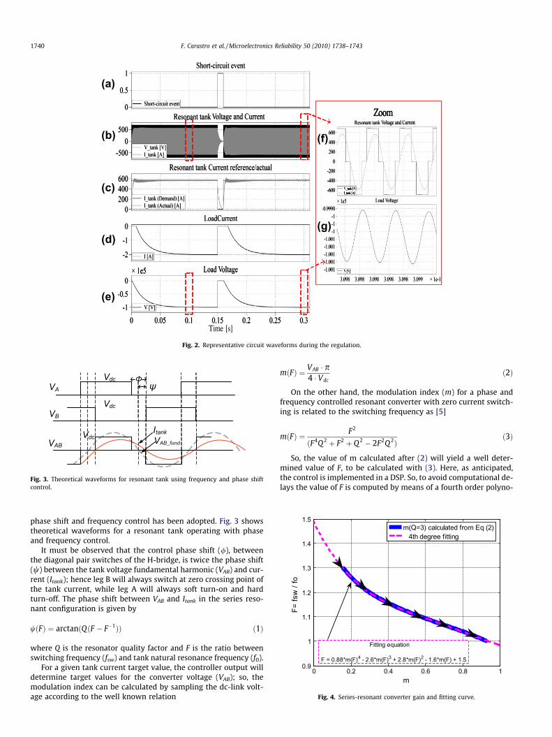
Fig. 2a–g shows simulation results for the proposed power sup-ply topology. Initially the power supply operates in the normalcondition; the current follows the reference current and the final100 kV output voltage is reached after 0.09 s. Fig. 2g shows the de-tail of the small load voltage ripple at the final condition. Moreoverduring this voltage regulation, as detailed in Fig. 2f, the chosentopology and control allow for zero current switching (ZCS) turn-on and zero voltage switching (ZVS) turn-off of the IGBTs of thelagging leg; however, the IGBTs of the leading leg experiencehard-switched turn-off commutations and require additionalsnubber capacitors to achieve low dissipation operation. Att = 0.15 s a short-circuit event, representing a spark between theEPS electrodes, occurs and the spark controller reduces the tankcurrent reference to zero. Fig. 2c shows that the tank current israpidly reduced to zero by the current controller, with a very lim-ited current spike, avoiding possible damage to the precipitator aswell as the power supply. When the short-circuit dies away thecontrol returns to voltage regulation mode and the voltage recov-ers at the maximum rate (corresponding to rated tank currentlimit).
Control of the power supply is implemented by means of both adigital signal processor (DSP) and a field programmable gate array(FPGA). The control platform also includes voltage and currentmeasurement to control the output voltage and for circuit protec-tion from destructive overloads.
3. Control strategy development
To control the tank current, hence the DC output voltage of theESP, whilst minimising the semiconductor losses, a combined
Zoom
Time [s]
(a)
(b)
(c)
(d)
(e)
(f)
(g)
Fig. 2. Representative circuit waveforms during the regulation.
VA
VB
Vdc
Vdc
VABItankVAB_fund
Φψ
Vdc
Fig. 3. Theoretical waveforms for resonant tank using frequency and phase shiftcontrol.
0 0.2 0.4 0.6 0.8 1
1
0.9
1.1
1.2
1.3
1.4
1.5
m
F= fs
w /
fo
Fitting equation
F = 0.88*m(F)4 - 2.6*m(F)3 + 2.8*m(F)2 - 1.6*m(F) + 1.5
m(Q=3) calculated from Eq (2) 4th degree fitting
Fig. 4. Series-resonant converter gain and fitting curve.
1740 F. Carastro et al. / Microelectronics Reliability 50 (2010) 1738–1743
phase shift and frequency control has been adopted. Fig. 3 showstheoretical waveforms for a resonant tank operating with phaseand frequency control.
It must be observed that the control phase shift (/), betweenthe diagonal pair switches of the H-bridge, is twice the phase shift(w) between the tank voltage fundamental harmonic (VAB) and cur-rent (Itank); hence leg B will always switch at zero crossing point ofthe tank current, while leg A will always soft turn-on and hardturn-off. The phase shift between VAB and Itank in the series reso-nant configuration is given by
wðFÞ ¼ arctanðQðF � F�1ÞÞ ð1Þ
where Q is the resonator quality factor and F is the ratio betweenswitching frequency (fsw) and tank natural resonance frequency (f0).
For a given tank current target value, the controller output willdetermine target values for the converter voltage (VAB); so, themodulation index can be calculated by sampling the dc-link volt-age according to the well known relation
mðFÞ ¼ VAB � p4 � Vdc
ð2Þ
On the other hand, the modulation index (m) for a phase andfrequency controlled resonant converter with zero current switch-ing is related to the switching frequency as [5]
mðFÞ ¼ F2
ðF4Q 2 þ F2 þ Q2 � 2F2Q 2Þð3Þ
So, the value of m calculated after (2) will yield a well deter-mined value of F, to be calculated with (3). Here, as anticipated,the control is implemented in a DSP. So, to avoid computational de-lays the value of F is computed by means of a fourth order polyno-

(a)Converter output voltage VAB
Output Voltage
Tank Current
F. Carastro et al. / Microelectronics Reliability 50 (2010) 1738–1743 1741
mial approximation of Eq. (3), as indicated in Fig. 4. Note that theconverter operates with a modulation index approaching unity(corresponding to the resonance frequency) when the controller(of PI type in this case) reaches steady state.
m=0.18
fsw=25.6 kHz
(b)
4. Experimental setup and results
Based on the electrical design a prototype converter has beenconstructed, shown in Fig. 5. Based on the resonant tank specifica-tion (f0 = 20 kHz), an inductor rated at a peak current of 600 A is re-quired. The design adopted is a ferrite (3C90) inductor with adistributed gap. The devices used for the H-bridge are standard800 A dual-switch IGBT modules. The step-up high frequencytransformer was assembled using U ferrite cores and Litz-wire.For this application a dry film metallized polypropylene dc-linkcapacitor optimized for high power applications (low ESR) hasbeen used.
m=0.7
fsw=21.2 kHz
(c)
4.1. Open-loop experimental results
Fig. 6 shows experimental open-loop results demonstrating theachievement of soft-switching of the IGBTs at different values ofthe modulation index. For the test an equivalent resistive loaddirectly connected at the transformer secondary side. It is possibleto observe that the intended soft-switching performances (seeFig. 3) have been achieved for all values of the modulation indexvalue.
m=0.9
fsw=20.2 kHz
Fig. 6. Experimental results at different operating points.
4.2. Closed-loop experimental results without voltage multiplier
Fig. 7a–c shows closed-loop experimental results, without thevoltage multiplier. It is possible to observe that the designed con-troller is capable of tracking the tank current demand as Fig. 7ashows. Fig. 7b–c shows also the detailed PI regulation perfor-mances; it is possible to observe that soft-switching is kept duringboth transient and steady state conditions. Fig. 8 shows the de-tailed output waveforms at full power during closed-loop steadystate operation. It is possible to observe that a maximum outputvoltage of 27.8 kV has been obtained. During this condition thecontroller is following a peak tank current demand of 600 A, deliv-ering an output power of 220 kW. Furthermore stable soft-switch-ing operation is maintained during the steady state conditions.These results verify the correct operation, in line with the electricaldesign.
Gate driver
H-bridgeDC-link
Controlplatform
Inprecti
Fig. 5. Converter protot
4.3. Closed-loop experimental results with voltage multiplier
In order to verify that soft-switching operational condition weremaintain even in the presence of the high capacitance introducedby the final configuration, the voltage multiplier has been con-
Resonantinductor
Resonantcapacitor
ut fier
ype and test setup.
Demand tank current
Converter output voltage
Actual tank current
Peak detector output(a)
(C) Zoom steady state(b) Zoom transient
Fig. 7. Experimental results during tank current regulation.
Capacitor tank voltage 1.9 kV
(a)
(b) Zoom
Converter output voltage 600 V
Output voltage 27.8 kV
Tank current 600A
Fig. 8. Full power closed-loop experimental results.
1742 F. Carastro et al. / Microelectronics Reliability 50 (2010) 1738–1743
nected at the transformer secondary terminals. It is possible to ob-serve that the presence of the voltage multiplier does not affect theperformance of the controller furthermore soft-switching opera-
tion is maintained during both transient and steady state condi-tions also in the presence of the voltage multiplier as detailed inFig. 9.

Zoom
DC output voltage
Converter output voltage
Transformer secondary voltage
Tank current
Fig. 9. Closed-loop experimental results with voltage multiplier.
F. Carastro et al. / Microelectronics Reliability 50 (2010) 1738–1743 1743
5. Conclusions
This paper has presented a control solution to ensure soft-switching of the semiconductor devices during all operationalmodes of a variable-frequency resonant converter supplying ahighly non-linear load. An analytical formulation of the controlstrategy has been presented and experimental results have beenprovided to support the validity of the envisaged solution. Furtherto enabling the achievement of the desired dynamic regulation ofthe output variables, the proposed approach allows for the optimi-zation of efficiency and the reduction of the electro-thermal stresslevel affecting the power switches.
References
[1] Mizuno A. Electrostatic precipitation. In: IEEE transactions on dielectrics andelectrical insulation, vol. 7, No. 5; 2000. p. 615–24.
[2] Grass N, Hartmann W, Klockner M. Application of different types ofhigh-voltage supplies on industrial electrostatic precipitators. IEEEtransactions on industry applications, vol. 40, No. 6; November–December2004. p. 1513–20.
[3] Durga Prasad NVPR, Lakshminarayana T, Narasimham JRK, Verman TM,Krishnam Raju CSR. Automatic control and management of electrostaticprecipitator. In: IEEE transactions on industry applications, vol. 35, No. 3;May–June 1999. p. 561–7.
[4] Carastro F, Clare JC, Castellazzi A, Johnson CM, Bland MJ, Wheeler PW.Reliability considerations in pulsed power resonant conversion. In: 20thEuropean symposium on reliability of electron devices, failure physics andanalysis ESREF; 2009.
[5] Bland M, Clare J, Zanchetta P, Wheeler P, Pryzbyla J. A high frequency resonantpower converter for high power RF applications. In: Power electronics andapplications, 2005 European conference, 11–14 September 2005; p. 1–10.