EGWafer Users Manual - us-isi.com Users Manual.pdf · In this implementation, the wafer prober is...
36
EGWafer User’s Manual Integral Solutions Int'l – Version 2.0.0 – March 30, 2010 Copyright ©2010 Integral Solutions Int'l All rights reserved Integral Solutions Int'l 3000 Olcott St Santa Clara, CA 95054 Phone: (408) 653-0300 Web: http://www.us-isi.com/ Fax: (408) 653-0309 E-mail: [email protected] While every effort has been made to verify the accuracy of the information contained in this publication, this publication may contain technical and/or typographical errors. Please contact Integral Solutions Int’l to report any errors in this publication.
Transcript of EGWafer Users Manual - us-isi.com Users Manual.pdf · In this implementation, the wafer prober is...

EGWafer User’s Manual Integral Solutions Int'l – Version 2.0.0 –
March 30, 2010
Copyright ©2010 Integral Solutions Int'l All rights reserved
Integral Solutions Int'l 3000 Olcott St
Santa Clara, CA 95054 Phone: (408) 653-0300 Web: http://www.us-isi.com/ Fax: (408) 653-0309 E-mail: [email protected]
While every effort has been made to verify the accuracy of the information contained in this publication, this publication may contain technical and/or typographical errors. Please contact Integral Solutions Int’l to report any errors in this publication.

EGWafer User’s Manual Integral Solutions Int’l March 30, 2010
Page 2
Contents
1 INTRODUCTION ...................................................................................................................................... 3
1.1 RELATED DOCUMENTATION ................................................................................................................... 4
2 INSTALLATION ....................................................................................................................................... 5
2.1 REQUIREMENTS ...................................................................................................................................... 5 2.2 ARRIVAL CHECKLIST .............................................................................................................................. 5 2.3 CONNECTIONS ........................................................................................................................................ 7
3 TESTER BASICS .................................................................................................................................... 10
3.1 STARTING PROBER ............................................................................................................................... 10 3.2 STARTING TESTER ................................................................................................................................ 11 3.3 TESTING WAFERS IN ENGINEERING MODE ........................................................................................... 12 3.4 TESTING WAFERS IN OPERATOR MODE ................................................................................................ 15
4 EGWAFER APPLICATION .................................................................................................................. 17
4.1 MAIN MENU ......................................................................................................................................... 18 4.2 WAFER SETUP ...................................................................................................................................... 21 4.3 WAFER DIE SELECTION (WAFER MAP) ................................................................................................ 24 4.4 TESTER OPTIONS .................................................................................................................................. 26 4.5 WAFER SN MODULE ............................................................................................................................ 27
5 ALIGNMENT PROCEDURES .............................................................................................................. 28
5.1 CHANGING PROBE CARD ...................................................................................................................... 28 5.2 CREATING WAFER SETUP ON THE PROBER ........................................................................................... 32 5.3 CREATING WAFER SETUP IN EGWAFER ............................................................................................... 33
6 APPENDIX ............................................................................................................................................... 35
6.1 EG PROBER GPIB SETTINGS ................................................................................................................ 35
7 LIMITTED WARRANTY ...................................................................................................................... 36
7.1 LIMITED WARRANTY. ........................................................................................................................... 36 7.2 OTHER LIMITS. ..................................................................................................................................... 36 7.3 EXCLUSIVE OBLIGATION. ..................................................................................................................... 36 7.4 OTHER STATEMENTS. ........................................................................................................................... 36 7.5 ENTIRE OBLIGATION. ........................................................................................................................... 36

EGWafer User’s Manual Integral Solutions Int’l March 30, 2010
Page 3
1 Introduction This document describes the set up and operation of ISI Wafer Level Analyzer (WLA)
based on Electroglass Horizon 4080 Wafer Prober. In this implementation Quasi97 is the master software controlling the overall test sequence, and EGWafer module is the driver that relays commands to the prober telling it when and where to move. This manual does not touch the actual tests run on the wafer, but focuses on the wafer and die setup and part selection for the test.
The WLA has two major components: the tester rack and the wafer prober. The tester rack contains a computer and some test equipment. Test equipment can vary depending on the application, however in all implementations it will include at least quasi-static tester QST-2002E and QPS-1050 power supply. Test equipment will be controlled from Quasi97 software. Any additional test modules that are installed in the rack are controlled through their respective tests that will be added to Quasi97 setup files via ActiveX interface (see “Add-Ins Selected Modules” in QST-2002 User’s manual).
Further the test rack is connected through an array of cables to the front end board(s) installed on the prober’s test head. Those in turn are connected to the probe card, which makes contact with dies on the wafer. The test head can also contain the magnet and the microscope. The microscope would have a camera feed going back to the PC inside the tester rack – this can be used during testing to monitor where the probes land.
The second component of the WLA is wafer prober. The prober is responsible for handling wafers to and from the cassettes, or the manual tray; loading the wafer onto the chuck, measuring the height of the wafer and doing the XY and Theta alignment. The prober keeps track of probe card Z and XY coordinates of the reference die on the wafer. Prober will also control the wafer temperature, if hot chuck option is installed.
In this implementation, the wafer prober is not responsible for stepping to different dies on the wafer, running tests scripts, or grading. The function of stepping to different devices on the wafer lies with EGWafer application that is running on the PC in the tester rack and communicating with the prober via GPIB interface. The EGWafer application can tell the prober to load the wafer, unload it where the prober will do all of the work. However, once the wafer is on the chuck, profiled and aligned – the EGWafer application takes over and commands the prober XY positions to move for testing.
The Wafer Prober and EGWafer are the primary topics of this manual.
EGWafer User’s Manual Integral Solutions Int’l March 30, 2010
Page 4
1.1 Related Documentation Quasi97 Software User’s Manual
Contains detailed description of all menus in Quasi97 software, along with procedures on how to set up test parameters, log data, and run the QST in production and engineering modes.
QST External Modules User’s Manual
Description of additional tests provided with the QST and Quasi97 software.
STT-MRAM Tests Users Manual
Test algorithms and menus if using the wafer prober for STT-MRAM memory testing.
RIA-2008 Users Manual
Test algorithms and menus if using ISI inductance measurement equipment.
FMRA Users Manual Test Algorithms and menus, if using ISI FMRA option and high frequency probes.

EGWafer User’s Manual Integral Solutions Int’l March 30, 2010
Page 5
2 Installation
2.1 Requirements • Compressed Air supply – at least 80psi, 3CFM • Vacuum Source – -22inchH • 115VAC (tester rack) • 100-220 VAC (prober) • Wafer Prober: 46”x40”x61” • Tester Rack: 24”x32”x45”
o Keyboard tray when opened adds 15” to the depth o Door when opened on the rack adds 21” to the depth
2.2 Arrival Checklist The WLA arrives in two crates, one for the prober and one for test equipment rack.
• Uncrate the prober a) Remove the front panel off the prober crate b) Remove the 4 screws on the right side panel,
holding the monitor rack. c) Remove the rest of the panels from the prober
crate. d) Move the prober off the pallet e) Remove the bubble wrap of the prober’s
monitor • Uncrate the tester rack a) Remove the front panel off the prober crate
b) Unscrew the ramps from the front panel and put them on the pallet
c) Wheel the rack off the pallet d) Remove shrink wrap from the test equipment
• Prepare the prober a) Connect the wafer prober to power outlet b) Connect wafer prober to compressed air and
vacuum supplies. c) Remove the tape holding the top access panel
and manual tray. d) Remove the tape holding cassette loader cover e) Remove the bubble wrap from inside the wafer
prober (wafer handler fork and the chuck) f) Remove the left top panel from the prober and
cut the tie wraps holding the chuck, but do not remove the pad from underneath the chuck until the prober is on.
• Prepare the rack a) Remove the shrink wrap from the test equipment
b) Plug in the tester rack to power outlet c) Connect the GPIB cable from the tester rack to
IEEE port on the wafer prober (NOT the “TESTER” port!)

EGWafer User’s Manual Integral Solutions Int’l March 30, 2010
Page 6
d) Turn on the rack e) Turn on the computer and pull out the monitor
tray • Remove the pad from
underneath the chuck a) Ensure the compressed air is ON. b) Raise the test head and remove the protective
cover (if present) on the probe card. Keep the test head raised until ready to test
c) Turn on the prober in the back and then in front. The prober will turn on the air to the chuck stage and start MS-DOS and then pause waiting for user response. DO NOT RESPOND UNTIL THE PAD IS REMOVED FROM UNDERNEATH THE FORCER
d) Take the forcer prying tool and insert on the right side of the forcer into specially designated holes. Push on the tool to lift one side of the forcer.
e) Slide the pad out from underneath the forcer f) Gently lower the forcer onto the plenum, by
releasing the prying tool • Calibrate the wafer prober a) Click any key on the prober’s keyboard to let
the machine continue startup. b) Once the EGCommander is loaded and prompts
for it – harbor the forcer c) After the EGCommander software completely,
go to Commands System Calibration click “Walk” button.
d) Follow prober’s prompts to complete system calibration.
• Connect the rack to the test head
a) Connect Universal interface through ribbon and two SMB cables to the rack.
b) Connect Magnet to the tester rack c) Connect the microscope camera to the rack d) Connect front-end board power to the rack e) The rest of the connection will be specific to
the application, but all the cables on the test head should be connected to the test rack
• Power ON the rest of the equipment on the test rack
a) Power on QST-2002E, QPS-1050, QMS-1050, FMRA*, RIA* and any other test equipment located on the rack
b) Run Quasi97 and open the last setup file on the tester
c) Ensure that no error messages appear during hardware detection. If error messages are present – check all cable connection or follow troubleshooting guide to fix the problem
d) Lower the test head and realign the probe card using manual-camera probe card alignment procedure on the prober.
EGWafer User’s Manual Integral Solutions Int’l March 30, 2010
Page 7
• Try a sample wafer a) Load a wafer, profile and align it using probers menu.
b) In EGWafer software, enable “Single Slider Mode”, move to one of the devices and run tests on it.
c) Check basic functionality of the tester (magnetic field, bias, pulsing, high frequency channel etc)
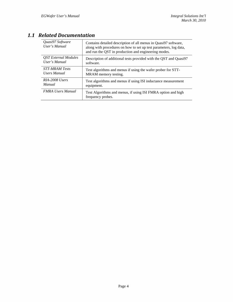
2.3 Connections The following connections are typical for the WLA. However your configuration may
have additional test modules, or not have some. QST-2002
USB To computer (digital IO) 14-pin round To QPS-1050 (DC power for QST-2002) BNC (Field 1) To QPS Splitter Input BNC (field output control) DB9 To QPS Splitter Input DB9 (QPS communication) SMB To RD OUT on universal interface board SMB To WD IN on universal interface board
QPS-1050
3pin AC Power To 115VAC outlet 14-pin round To QST-2002 (DC power for QST-2002) 9-pin round To quad-pole magnet 2-pin Female connector for Transverse coils BNC To QPS Splitter Output BNC X (field output control) DB9 To QPS Splitter Output DB9 X (QPS communication)

EGWafer User’s Manual Integral Solutions Int’l March 30, 2010
Page 8
QMS-1050B
3pin AC Power To 115VAC outlet 9-pin round To quad-pole magnet 2-pin Male connector for Longitudinal coils BNC To QPS Splitter Output BNC Y (field output control) DB9 To QPS Splitter Output DB9 Y (QPS communication)
QPS Splitter
USB To computer (digital IO) DC Power Inlet No Connect Input BNC To QST-2002 Field 1 output Input DB9 To QST-2002 DB9 Output BNC X To QPS-1050 BNC Output DB9 X To QPS-1050 DB9 Output BNC Y To QMS-1050B BNC Output DB9 Y To QMS-1050B DB9 Output BNC Z No Connect Output DB9 Z No Connect
Quad-pole Magnet
2-pin Female To QPS-1050 9-pin round connector 2-pin Male To QMS-1050B 9-pin round connector
2xBar Gen3 Interface Board / Universal Interface
60pin ribbon To QST-2002E 2x SMB To QST-2002E (RD OUT and WD IN connection)

EGWafer User’s Manual Integral Solutions Int’l March 30, 2010
Page 9
2x SMB From universal board to 2xBar G3 board 50pin ribbon From universal board to 2xBar G3 board 40pin ribbon 2xBar Gen3 Intermediate board assy 2x Black SMB 2xBar Gen3 Intermediate Board Assy CH0 ribbon probe card cable
To the left side of the probe card on the test head

EGWafer User’s Manual Integral Solutions Int’l March 30, 2010
Page 10
3 Tester Basics
3.1 Starting Prober The prober should have compressed air and vacuum sources on prior to turning on. To
turn on the prober, click the “ON” button in the bottom right corner of the prober. The MS-DOS on the prober will start and prompt operator to click a key to continue loading EGCommander software – click spacebar.
Then the prober will ask “Start handler initialization” – the operator can click F10 on the prober keyboard or select “OK” on the touchscreen. Next the prober will “blank the forcer” and ask operator to “harbor the forcer”. This is homing sequence, where operator should open the front left panel and move the forcer to the front left corner of the plenum. At that point operator should close the front left access panel and then click “OK” and the forcer will energize. Then the front panel should be closed and operator should click “Verify” and the prober will verify that home position is correct by moving the chuck’s feducial point under the bridge camera.
Once the initialization sequence is complete, the prober will show “Command” menu, which operator can use to load wafer, profile, align or to change probe card. Before loading the wafer the operator should ensure that correct product file (with wafer parameters) is open. Product file can be selected from Product Select.

EGWafer User’s Manual Integral Solutions Int’l March 30, 2010
Page 11
3.2 Starting Tester Each module on the test equipment rack has its own power switch. The order in which
components are turned ON is not important. However, it is important to start the Quasi97 software only after all of the required test equipment was turned on and the wafer prober initialized.
Figure 3-1 - Starting Quasi97
Quasi97 software will detect the installed options and read off the calibration factors from EEPROMs in the QST-2002E. Then Quasi97 will start EGWafer driver and prompt for test script selection. If EGWafer application does not start, then operator needs to select EG Wafer on the Setup Selection dialog. When EGWafer starts, it will show violet disk icon in the system tray, which can be used to invoke its operator menu.
Figure 3-2 - Quasi97 Setup Selection Dialog
User should then select one of the available test scripts or create his or her own. After selecting test setup file, user can start testing dies on the prober.

EGWafer User’s Manual Integral Solutions Int’l March 30, 2010
Page 12
3.3 Testing Wafers in Engineering Mode Quasi97 has two modes: operator and engineer. In engineer mode, user can change the
test parameters, test sequence, and all other options. Engineer can also run a few parts from the wafer to verify test parameters.
Operator mode allows user to start running production test or abort it, change the log file and select which devices to test from the wafer map. To switch between engineering and operator mode, user can go to File Operator Log In and in the prompted dialog box type in the password. If the password matches with whatever is in tools options, then software will go to engineering mode – all other passwords will force operator mode. The password can be different for each test script, and there is an option to prompt operator login after opening the setup file (refer to QST-2002 Users manual for more information).
User can load the wafer from manual tray, or from the cassette, then profile and align the wafer using the prober’s menus. To do this, select the command using the touchscreen and click execute.
Alternatively user can click “Handler Load, Profile and Align” in the EGWafer menu.
Once the wafer is loaded and aligned, Quasi97 can start probing dies. If the wafer was already loaded on the chuck prior to starting the software then “Load,
Profile and align” is not necessary, user can go straight to probing sliders. If user prefers to load,

EGWafer User’s Manual Integral Solutions Int’l March 30, 2010
Page 13
profile and align wafer using the prober interface, then after alignment, user should click EGWafer Hander Check New Wafer Center.
Single Slider Mode
The simplest mode of operation that does not require setting up the wafer in EGWafer application is the single slider mode. This mode can be enabled in EGWafer software.
Figure 3-3 - EGWafer Single Slider Mode
Here user can move manually to any XY position on the wafer, then click “START” button in Quasi97 and run any test. Note that Quasi97 does not turn off bias automatically here, and user should click “STOP” button in Quasi97 prior to moving to a different site on the wafer.
User can move the chuck using the joystick on the prober. The joystick has 3 modes of operation: jog, index and scan. In addition to this the joystick has a “turbo” button. Pressing that button in conjunction with moving the joystick runs the selected same mode faster. To switch between the modes twist the joystick around its vertical axis (clockwise or counterclockwise) – the mode will be displayed in the top right corner of the prober’s display.
The jog mode moves in smallest increments; the index mode moves one die size at a time as defined in the Prober’s setup; the scan mode moves using fixed velocity and stops when the joystick is returned to center position.
EGWafer User’s Manual Integral Solutions Int’l March 30, 2010
Page 14
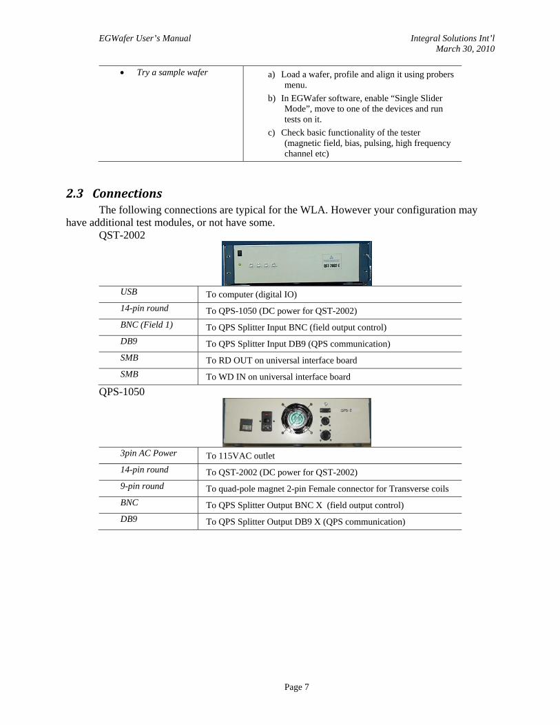
Row / Column Mode Once the wafer is defined in EGWafer software, user can move between sites using
“Block, Row and Column” addressing. In this mode, when user clicks start – EGWafer enables as many heads in Quasi97 software as there are columns in the selected row. Then user can iterate through the devices by changing the head # in the lower right corner of Quasi97 screen.
Figure 3-4 - Block,Row,Column Die Selection
The block can be selected from the combo box. The row and column can be selected by typing in the row and column numbers and clicking “GO!” button, or by using the arrow key buttons. User can confirm the current location on the wafer, by clicking the “Video” button and looking at the probes through the built in microscope.
In engineering mode, user can select any head and run a single test on it. Or if desired user can select “Production Test” and run it on all the columns in the selected block and row. This mode can be useful to check test scripts on several dies before running on the whole wafer, or to check repeatability of the results.

EGWafer User’s Manual Integral Solutions Int’l March 30, 2010
Page 15
3.4 Testing Wafers in Operator Mode In operator mode, user can select the dies to test through EGWafer Map and then click
“Quasi97 START” to commence testing. The dies that are turned ON and marked as untested in the EGWafer map will be probed and tested. After testing each die, it will be marked in the map according to its grade. Because of the test outcome is recorded after every slider, if the test is aborted, user can continue from where it left off without doing any changes to the map.
Figure 3-5 - Wafer Die Map
There are several options available for the operator: • Test Single Block • Test Wafer • Test Cassette
These options are located in EGWafer’s main menu. In case of single block, the test will stop after all selected rows and columns on the current block are tested. With test wafer option, the test will stop after all the blocks are tested on the wafer.
Figure 3-6 - Operator Test Mode
Lastly with Test Cassette option, upon completing testing the wafer, the EGWafer software will attempt to load the next wafer from the cassette. Once loaded onto the prober, the cassette has to be mapped through the EGCommander software (Prober’s command menu). Go

EGWafer User’s Manual Integral Solutions Int’l March 30, 2010
Page 16
to Prober Cassete Map to do this. After the mapping, operator can go to “View/edit cassette” and enter the wafer IDs for all the wafers that the system detected.
During production test, in the test cassette option, after a single wafer is tested an unloaded back to the cassette, the wafer map is reset, ie for all dies that are enabled in the wafer map, the test outcome will be changed to untested.
Note that for any for any option in the operator mode – the “Single Slider Mode” and “Broken Bar Mode” should be disabled.

EGWafer User’s Manual Integral Solutions Int’l March 30, 2010
Page 17
4 EGWafer Application The EGWafer module is a standalone application that can be used to tell the Electroglass
prober where to move on the wafer, probe and unprobe. It can also do other miscellaneous operations, like loading and aligning the wafer.
Quasi97 uses EGWafer module as a driver. Through ActiveX interface Quasi97 calls functions within EGWafer prober, telling it when the test is started, completed and when to move to a different die. EGWafter on the other hand, tells Quasi97 how many devices to and uses the information passed back from Quasi97 to update test outcomes of dies on the map.
After every slider selection, EGWafer module changes the PartID and Head label, and Part Reference fields in Quasi97. So each test result logged by Quasi97 can include the PartID (wafer serial number), the Head Label (die name on the wafer, per user defined naming convention) and Part Reference (indicating offset of the part probe from the center of the wafer in um).
Figure 4-1 - EGWafer Fields in Info
When EG Wafer configuration is selected in Quasi97, the module adds a “Slider Info” test to the “Static Tests” collection, which can supply more information about the die under test.
Figure 4-2 – EGWafer’s Slider Info Test
EGWafer User’s Manual Integral Solutions Int’l March 30, 2010
Page 18
4.1 Main Menu The EGWafer’s main menu will appear first, if EGWafer is started on its own. If
EGWafer is started from Quasi97, then its main menu is accessible by all of these means: 1) By clicking the purple ¼ disk icon in the system tray
2) By clicking to Quasi97 File Device Setup 3) By clicking to Quasi97 System System Device Setup 4) By clicking to Quasi97 Peripherals EGWafer
The main menu allows basic navigation on the wafer, probe/unprobe actions as well as gives access to wafer setup, wafer map, prober diagnostics and others.
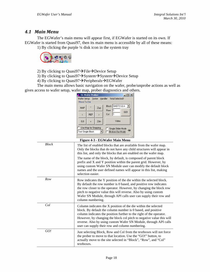
Figure 4-3 - EGWafer Main Menu
Block The list of enabled blocks that are available from the wafer map. Only the blocks that do not have any child structures will appear in this list, and only the blocks that are enabled on the wafer map. The name of the block, by default, is composed of parent block prefix and X and Y position within the parent grid. However, by using custom Wafer SN Module user can modify the default block names and the user defined names will appear in this list, making selection easier.
Row Row indicates the Y position of the die within the selected block. By default the row number is 0 based, and positive row indicates the row closer to the operator. However, by changing the block row pitch to negative value this will reverse. Also by using custom Wafer SN Module, through API calls user can supply their row and column numbering.
Col Column indicates the X position of the die within the selected block. By default the column number is 0 based, and positive column indicates the position further to the right of the operator. However, by changing the block col pitch to negative value this will reverse. Also by using custom Wafer SN Module, through API calls user can supply their row and column numbering.
GO! Just selecting Block, Row and Col from the textboxes will not force the prober to move to that location. Use the “GO!” button, to actually move to the site selected in “Block”, “Row”, and “Col” textboxes.

EGWafer User’s Manual Integral Solutions Int’l March 30, 2010
Page 19
Video Button to turn on the video feed from the microscope located directly above the probes. Note that the LED intensity is controlled manually from the LED power supply on top of the tester rack.
REF This button moves the wafer, such that the reference die is under the probes. The location of reference die vs the probes is set in the EG Prober and is completely independent of wafer setup in EGWafer software.
0,0 Moves the wafer, such that the first die in the selected block is under the probes (row 0 & column 0).
Zup Probe command. Move to Z probe position + Z overdrive as defined in the prober.
Zdn Unprobe command. Moves some distance below the probes, such that it is safe to move around. Note that this command is optional – when moving between dies, the prober will recognize when its probing. If probing the prober will move down to clear the probes first, then will move to the target wafer location and move back up to probe.
Map Shows the map of the currently selected block. In the map menu user can go to parent block or any other block on the wafer and change which dies are ON and the test outcomes.
UP/Down Arrows Move to different row in the selected block Left/Right arrows Move to different column in the selected block Use Map for Stepping
If enabled, then when using UP/DOWN and Left/Right arrows, the prober will skip the sliders that are turned Off in the map. Note that the prober can appear to be stuck in one location if none of the rows in the selected column are enabled (or columns in the selected row).
Test Single Block Test Wafer Test Cassette
Options for the operator mode in Quasi97. Tell the software whether to run only the selected block, the full wafer, or all the wafers in the cassettes. Note that with any one of these options selected, the software will only test dies that are marked enabled and untested.
Single Slider Mode If enabled in engineering mode, EGWafer application will set the number of heads in Quasi97 to 1. When user would press START or STOP in Quasi97, the software simply will go to probe and unprobe, without moving the wafer on XY plane. This mode is can be used to manually move the wafer using the joystick on the prober and test that single site.
Broken Bar Mode Normally not used. Similar to single slider mode, but the user gets to define a single row of dies to be tested. With this option the user can select the starting XY position, the last XY position and the number of dies. Then by selecting different heads in Quasi97, user will be able to go to any one of the dies in the defined row.
Pushpin Keeps the EGWafer main menu on top of other menus.

EGWafer User’s Manual Integral Solutions Int’l March 30, 2010
Page 20
EGWafer Menues Total Selected? Calculates how many dies are selected on the wafer map (dies that
are ON and marked as UNTESTED). Displays that information in the status bar of EGWafer main menu.
Wafer Setup Describe Wafer
Menu to define block structures on the wafer.
Wafer Setup Wafer Setup
Displays the list of the blocks and their coordinates with respect to the wafer center in a table. This can be used for diagnostics – none of the changes made in that menu will stay.
Wafer Setup Wafer Map
The actual map of the wafer, where user can enable/disable dies, and change die test outcome.
Tester Options Tester options are saved in the EGSetup.ini file, and can be modified through this menu. These are general options, GPIB address of the prober, the name of the video applicat, the default wafer setup selection, log file options etc.
Tester Probe Card Alignment
This menu can be used to change the probe card alignment, such as after changing chuck temperature
Tester Diagnostics Prober Diagnostics menu. This can be used to check probe communication or send some commands to the prober through GPIB interface.
Handler Load, Profile and Align
This command will try to load the wafer from the cassette, if the wafer is not already loaded on the chuck. Then it will try to profile the wafer on the chuck, if the wafer is not already profiled. Then it will align the wafer on the chuck, if the wafer was not aligned already. Lastly, EGwafer will read of feducial point (XY position of the reference block) from the prober.
Handler Load Next Wafer
If wafer is loaded on the chuck, then this command will unload the wafer first to the original location in the wafer cassette (or manual tray), then will load the next wafer from the cassette, profile and align it.
Handler Unload Unloads the wafer from the chuck to its original slot in the cassette or to the manual tray (if it was loaded from there).
Handler Check new wafer center
The function will read feducial point (XY position of the reference block) from the prober. This may be necessary, if operator went through EGCommander to load, profile and align the wafer.

EGWafer User’s Manual Integral Solutions Int’l March 30, 2010
Page 21
4.2 Wafer Setup Wafer setup is stored in Microsoft access database format, in the file with the extension
mdb. From the main menu, user can create a new wafer setup, save the current setup under different name, or open an existing setup. The wafer setup stores the meta information about the wafer (all the structure definition), and the actual wafer maps.
The first menu user should access to define the wafer is “Describe Wafer”. In this menu, user can set the wafer size, the production test order, and the information about wafer blocks.
Figure 4-4 - Describe Wafer
In EGWafer software all die stepping is build on the blocks. The block a 2 dimensional array of dies, in which dies are spaced using a single row and column pitch. Each block can have child blocks, or another grid of dies with fixed row and column spacing. Only the blocks that have no child blocks, as defined in this menu, will be used for testing.
User can have more than one block structure at any level of the hierarchy, and blocks with 1 row and 1 column are allowed by the software. Each block structure can be anchored to a location on the wafer, by specifying the reference Col die#, row die#, ref col position (X) and ref row position (Y). The wafer map on the right side, shows the approximate position of the block on the wafer, based on these numbers.
When defining the new wafer, user should click “Set Ref Die Offs”, which will calculate the distance from the reference X and Y block on the wafer to the center of the wafer. Rather than using the center of the wafer (which tends to move around on the prober after redefining wafer position), the prober’s reference block XY position is used as a starting point. All positions used and reported in the EGWafer software are still center of the wafer based.

EGWafer User’s Manual Integral Solutions Int’l March 30, 2010
Page 22
Wafer Size The size of the wafer in mm. Used only to scale the block position
and size on the wafer diagram. Not used on the prober or to calculate any die position.
Operator Description
The comment for the operator, if the file name is not easily recognizable. This is user field, and is not used by EGWafer software.
Wafer SN App The name of the ActiveX application and class that will convert the block names from EGWafer number scheme to user numbering scheme. When EGWafer is installed, it copies WaferSN visual basic project on the target hard drive. User can rename this project, modify it and compile. Then it can be used in this setting to better orient o the wafer map. To enable the sample wafer SN app, type it waferSN.clsWaferSN here.
Set Ref Die Offs This will inquire from the prober the location of the reference die, and the location of the center of the wafer, and will calculate the offset of the reference die to the center. Reference block XY position is more stable than wafer center position. Any time the wafer is loaded, XY position of the reference block will be read from the wafer and used in conjunction with ref die offs to calculate the actual motor position to go to any dies on the wafer.
Production Order Row col or Col Row – this defines whether the rows are incremented first then columns, or columns first then rows.
Map # Add/Remove Map
The wafer map is stored in the mds file under map#. This selection can help user select different wafer maps on the wafer quickly.
Wafer Block Add Remove Add Child
This defines the hierarchy of blocks on the wafer. Note that after adding a new block, it is a good idea to give it a meaningful name. Block name has to be unique for the wafer and can not be numeric. The order the blocks appear here, will also have an effect of the order they are tested in production test.
Block Definition
Block Name The name of the block for the easier reference. Parent Shows the name of the parent block of the selected item on the block
tree. Comment User field - can be any user comment. Enumerator Prefix This is important setting, as it will be used to build the name of the
block. For example the name of the block is S (0,5) D (1,1) – which is S for the parent block and D for the child block. That name would indicate block is located on row 0 and column 5 within the block structure S; and on row 1 and column 1 within substructure D.
Color TBD Columns Number of blocks (dies) on X axis in the selected grid. Rows Number of blocks (dies) on Y axis in the selected grid.

EGWafer User’s Manual Integral Solutions Int’l March 30, 2010
Page 23
Column Pitch The distance in um from die 0,0 to die 0,1 Row Pitch The distance in um from die 0,0 to die 1,0 Ref Col Die # The Die number (1 to Columns), which will be used to calculate the
X offset of the selected grid from the center of the wafer, or from the location of the parent block (if parent block exists).
Ref Row Die # The Die number (1 to Rows), which will be used to calculate the Y offset of the selected grid from the center of the wafer, or from the location of the parent block (if parent block exists).
Ref Col Pos Offset from the center of the wafer (in um) of the Ref Col Die # Ref Row Pos Offset from the center of the wafer (in um) of the Ref Row Die # Calculate Ref X and Y Pos
Move the wafer such that the reference die of the selected structure is under the probes and click this button to find set Ref Col Pos and Ref Row Pos
Build Wafer Map Use this button to build wafer map (only then map becomes useful). Also if you change the number of rows or columns in any block or number of block structures, the wafer map needs to be rebuild.
Floppy Disk Save wafer setup

EGWafer User’s Manual Integral Solutions Int’l March 30, 2010
Page 24
4.3 Wafer Die Selection (Wafer Map) The wafer map menu should be used to enable/disable dies and change their test
outcomes. On the left side of the menu, user can control which blocks to display, whether to display die enable or test outcome on the wafer map; and helpful commands such as copy and paste. On the bottom right, the wafer diagram shows the approximate location of the block on the wafer.
On the right side of the menu the map is displayed.
Figure 4-5 - Wafer Map Menu
Block Selection Block Type Tree On the left top, there is a tree with all block types defined for this
wafer. User can hide some of the blocks in the “Block” combo box, but unchecking one or a few of these. At least one block type should be enabled in this tree.
Block combo box This selects what block is shown on the right side of the menu. Go Parent Goes to the parent of the block shown on the right. Once the parent
is displayed, the row and column of the current block is selected. Go Child Looks up the child block of the one selected in the map on the right. Block Enable The enable checkbox shows whether the block is enabled in general.
Block will be disabled if any one of its parents is disabled.

EGWafer User’s Manual Integral Solutions Int’l March 30, 2010
Page 25
Die Selection Show Enabled 0 - Untested 1 – Failed 2 – Passed Grade 1 …
Each die has an enable/disable flag and test outcome number. This combo box controls what to show on the map. The enable/disable flag is permanent selection and will stay when resetting the map. The test outcome is volatile selection, which is valid for the currently loaded wafer, but may be reset for the next. To change die enable, simply click on the checkbox for that die. To change test outcome, select the corresponding cell in the wafer map and change the test outcome number to new one.
Column Select If this option is on, then after changing the die enable/disable or its test outcome – all the dies in the column will be updated to have the same value for die enable (or test outcome if show option is set to 0 or higher)
Row Select If this option is on, then after changing the die enable/disable or its test outcome – all the dies in the row will be updated to have the same value for die enable (or test outcome if show option is set to 0 or higher)
Select All In Block Will change test outcome for all sliders in the selected block to 0 - Untested.
Clear All in Block Will change test outcome for all sliders in the selected block to 2 – Tested Passed Grade 1.
Reset Wafer Map Resets the test outcomes of all dies that are ON to 0- untested. ON:XX TestOutcomes:YY
Shows how many dies in the current block are turned ON and how many have the same test outcome as selected in the “Show” menu.
Apply Map To All Blocks
Will propagate die ON/Off selection to all blocks of the same type. In case show option is set to 0 or higher, then will propagate die test outcome selection to all blocks of the same type.
Copy Map Will remember the block for which you made the selection (it does not put anything in the clipboard).
Paste Map Will look up the remembered block and apply the same die ON/Off selection to the current selected one. If Show option is set to 0 or higher, then will copy test outcomes instead.
SQL Selection
This option allows to update the database directly for the currently selected block. In some cases this will be faster than selecting dies by clicking them on the map. For example, the SQL line:
DieSkip=1, TestOutcome=0 WHERE (DieCol=4 OR DieCol=5) AND (DieRow>2 AND DieRow<8)
Equates to UPDATE WaferMap SET DieSkip=1, TestOutcome=0 WHERE ((DieCol=4 OR DieCol=5) AND (DieRow>2 AND DieRow<8) and Block=BB)
User can use standard SQL logic expressions, and setting both DieSkip and TestOutcome is not necessary. These can be set independently.

EGWafer User’s Manual Integral Solutions Int’l March 30, 2010
Page 26
4.4 Tester Options This menu should be used to set global options for all wafer setups.
Figure 4-6 - Tester Options Menu
GPIB Address The GPIB address of the prober. This must match with whatever is selected on the prober.
Video Driver The name of the video application that will capture the video feed from the microscope located above the probe card. Default is vdmatrox8.driver
Default Wafer Setup File:
The name of the wafer setup file that was last opened. When restarting the software – this wafer setup file will be opened automatically.
Default Wafer Map #
NOT USED
PreProbe XOffset YOffset Delay (mS)
If enabled, before going to a die, this option will force prober to move to the die X position +Xoffset, die Yposition+YOffset; then probe and wait for the specified delay. This can be used to remove the initial charge on the devices, if the backplane of the wafer is not grounded.
Connect Will try to connect to EG prober using the new specified GPIB address.
Show Control Windows
Will display the video application’s main menu. This can be used to mirror the acquired image.
Auto Log File Change Options
If enabled, will track the current wafer ID, block type, block, row and column, and automatically change the log file if those change. This option can be used to trim the log file size.
Use CH1 If the probes are installed on the right side of the magnet, then this options should be enabled. Such as in the case of FMRA tester.

EGWafer User’s Manual Integral Solutions Int’l March 30, 2010
Page 27
4.5 Wafer SN Module The module allows modification of the block and row/col numbering scheme, such that it
matches user’s documents. The module is written in Visual Basic 6, and is an ActiveX dll with one public interface class. The class should have 4 public properties to work with EGWafer:
Public Sub GetRealFromUserSTR(usrRow$, usrCol$, row%, col%, block$) Public Sub GetUserFromRealSTR(usrRow$, usrCol$, row%, col%, block$) Public Function GetUsrBlockFromReal(block$) As String Public Function GetHeadSNStr(row%, col%, block$) As String GetRealFromUserSTR function should return row and col, which are passed by
reference. EGwafer will call this function and supply usrRow, usrCol and the name of the block (EGWafer name created using block prefixes). For example, if user row and column start from 1 instead of 0, then this function could do the following
Row = usrRow-1 Col = usrCol-1 GetUserFromRealSTR function should return usrRow and usrCol, which are passed by
reference. EGwafer will call this function and supply Row, Col and the name of the block (EGWafer name created using block prefixes). For example, if user row and column start from 1 instead of 0, then this function could do the following
usrRow = Row+1 usrCol = Col+1 GetUsrBlockFromReal function should return the name of the block as user wants to see
it. EGWafer will pass the name of the block created using prefixes, then user can parse out that name to figure out which exact block that is and create a different one. As an example the user can rearrange row and column number of the block.
GetHeadSNStr function should return the actual head label that the user wants to use for
the die under test. EGwafer will supply 0-based row number, column number and the name of the block (egwafer name created using block prefixes). User can then create a custom name and return it – this will appear on virtually every plot and in the result info. For example
GetHeadSNStr = GetUsrBlockFromReal(block) & " x" & CStr(row +1) & "y" & CStr(col +1)

EGWafer User’s Manual Integral Solutions Int’l March 30, 2010
Page 28
5 Alignment Procedures
5.1 Changing Probe Card There are several ways to update the probe card position: manual and manual-cam. With
manual way, user needs to load the wafer and move the reference die under the probes, then move on Z to until the probes touch the pads and set Z work. Manual way is best used if the probe card position was set by manual-camera procedure, and now needs to be slightly realigned. If manual-cam procedure never ran, it could be a chore to find put the probes on the right die.
With manual-cam mode, user needs to define pads on the wafer first, then unload the wafer and then run probe card alignment using up-facing (DPS) camera on the prober.
Manual Probe Card Alignment procedure: 1) Load the wafer on the chuck, profile and align it. 2) Go to EGCommander Commands Set Probes-to-Pads
3) Select “Manual” 4) Move the wafer on XY such that the probes land on the right set of pads on the
reference die. Use the joystick on the prober to do this 5) Then use Z jog up/down buttons to move the chuck up to contact. Monitor the
progress on the microscope camera (tester PC). Once the probes start scrubbing – stop and click “Z Work” on the wafer prober.
6) Click F10 to close the menu and remember XY position of the chuck. 7) In EGWafer software, click Handler Check new wafer center position.
Manual-Cam Probe Card Alignment procedure: 1) Load your target wafer, profile and align it. 2) In EGCommander go to Product Cntrl Map Pads 3) Delete whatever preexisting pads were there. 4) Click “Train” to train new pads. 5) Move the chuck, such that the crosshair on the screen is over the first pad. Once the
crosshair is aligned - click “Turbo button on the joystick. The EGCommander should say Pad 1 set.
6) Continue setting other pads.
EGWafer User’s Manual Integral Solutions Int’l March 30, 2010
Page 29
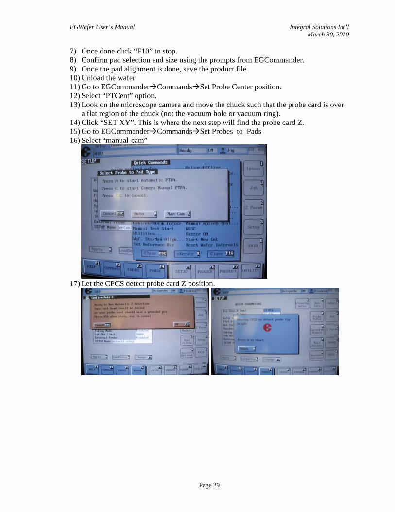
7) Once done click “F10” to stop. 8) Confirm pad selection and size using the prompts from EGCommander. 9) Once the pad alignment is done, save the product file. 10) Unload the wafer 11) Go to EGCommander Commands Set Probe Center position. 12) Select “PTCent” option. 13) Look on the microscope camera and move the chuck such that the probe card is over
a flat region of the chuck (not the vacuum hole or vacuum ring). 14) Click “SET XY”. This is where the next step will find the probe card Z. 15) Go to EGCommander Commands Set Probes–to–Pads 16) Select “manual-cam”
17) Let the CPCS detect probe card Z position.

EGWafer User’s Manual Integral Solutions Int’l March 30, 2010
Page 30
18) In the next dialog box (where the pads are shown), click “Camera” button.
19) Move the chuck until you see the tip of the probes on the screen. Align the probe tip
of the selected pad to the crosshair.
20) Confirm alignment using high magnification camera.
21) Now click “Close” or F10 to finish. Finding other pads is not recommended as it can
mistakenly lead the prober to believe that the probe card is at an angle, and the prober would try to compensate by rotating the chuck.
EGWafer User’s Manual Integral Solutions Int’l March 30, 2010
Page 31
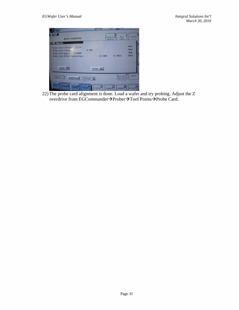
22) The probe card alignment is done. Load a wafer and try probing. Adjust the Z
overdrive from EGCommander Prober Tool Points Probe Card.

EGWafer User’s Manual Integral Solutions Int’l March 30, 2010
Page 32
5.2 Creating Wafer Setup on the Prober Each wafer design requires product file on the prober. The prober stores information such
as wafer diameter, alignment patterns, pad shape size and location, die pitch and others. The following procedure describes the step needed to do this. All of the following steps need to be done in the EGCommander software, using the Probers input interface.
1) Go to product, click “Select”, then type in a new file name and click “Save as”. This will create a new product file.
2) In Product Control map, change the wafer diameter and the die size. In case of really small die sizes, it may make more sense to set the die size equivalent to a group (or a block) of dies. Then in EGWafer define finer structure.
3) Change the wafer loading angle. For this check how the probes are set up on the probe card.
4) Load the wafer 5) Profile the wafer 6) Click “Find Target” 7) Follow the prompts of the prober to select unique target on the screen. If
this is not working, you may have to go to product options and change the Alignment/WSSC settings to match your wafer.
8) If successful the prober should be able to align the wafer. 9) Set the reference die when prompted. Since EGWafer software does not
use reference die numbers, it is not important which one would be reference. However, if you want the Prober’s wafer diagram to show which die you are on, you may need to adjust the reference die numbering under product Cntrl Map.
10) Skip pad detection (click escape). The pad detection can be done separately as part of the probe card alignment procedure.
11) Go to product Select and click Save. 12) In the EGWafer software, click Handler Check new wafer center
position.

EGWafer User’s Manual Integral Solutions Int’l March 30, 2010
Page 33
5.3 Creating Wafer Setup in EGWafer EGWafer is responsible for XY stepping, once the wafer is loaded on the chuck. Through
this software user can select which dies to test, so it needs to be aware of the die pattern on the wafer. Almost all of the steps in this procedure will be done in EGWafer Wafer Setup Describe Wafer.
Figure 5-1 - Creating Wafer Setup in EGWafer
The first step for the user is to identify the repeating patterns on the wafer. The wafer will be separated into grids, of X columns and Y rows and each. Each die in the grid can be represent another grid on its own. Once that is determined, user can load the wafer and easly set up the block structure by moving the wafer to various blocks.
1) Create a new wafer setup file (mdb file) 2) Set Wafer Size 3) Load a wafer using the prober, then profile and align it. 4) Click Handler Check new wafer center 5) In Describe Wafer menu, click “Set Ref Die Offs”. This will save the distance of
the reference die with respect to the wafer center. If you change the reference die though the prober, you will need to update this.
6) Click add, under wafer blocks. 7) Give the block unique name and unique prefix 8) Set number of columns, rows 9) Set the column pitch and row pitch in um. The default coordinate system is such
that positive direction on X (Columns) is moving to the right of the wafer. Positive direction on Y (rows) is moving towards the bottom of the wafer. So if user coordinates are different, set the corresponding pitch to negative number.
10) Move the wafer such that one of these blocks is under the probe card (use microscope camera feed). The best thing to do is to move to a corner of the wafer, where the position is clearly identifiable.
11) Set Ref Col Die #, and Ref Row Die # - this is the XY address of the block in the grid.
12) Click “Calculate Ref X and Y Pos”. 13) If the block is another grid, then click “Add Child” and define the child block.

EGWafer User’s Manual Integral Solutions Int’l March 30, 2010
Page 34
14) For setting the Ref X and Y Pos of the child block, you must stay within the same parent die.
15) Continue to set all blocks on the wafer. 16) Once finished, click “Build Wafer Map” 17) Then click the floppy disk button to save the setup. 18) Go to Wafer Setup Map and deselect all dies that do not exist on the wafer (the
wafer is usually round and the grid structure is square, so most often you will have to disable some dies).
19) Save Wafer setup file.
EGWafer User’s Manual Integral Solutions Int’l March 30, 2010
Page 35
6 Appendix
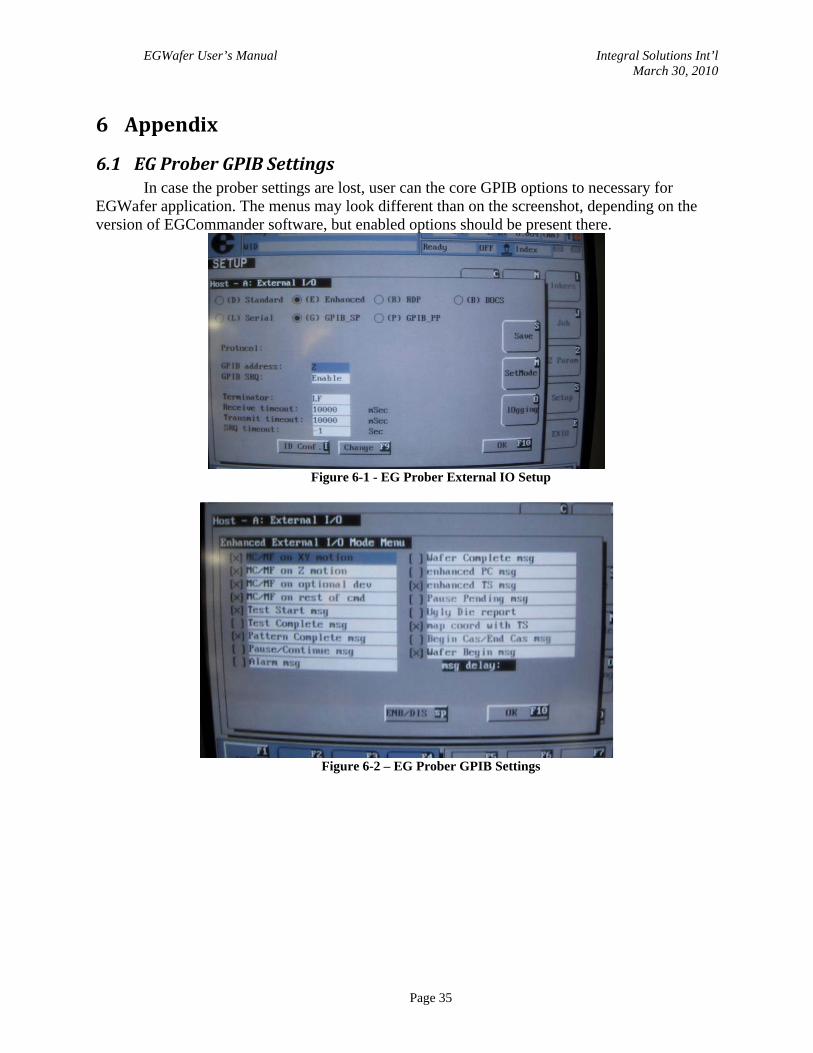
6.1 EG Prober GPIB Settings In case the prober settings are lost, user can the core GPIB options to necessary for
EGWafer application. The menus may look different than on the screenshot, depending on the version of EGCommander software, but enabled options should be present there.
Figure 6-1 - EG Prober External IO Setup
Figure 6-2 – EG Prober GPIB Settings

EGWafer User’s Manual Integral Solutions Int’l March 30, 2010
Page 36
7 Limitted Warranty Integral Solutions Int'l, a California Corporation, having its principal place of business at
3000 Olcott St, Santa Clara, CA 95054 ("Manufacturer") warrants its Quasi-Static Tester model QST-2002 products (the "Products") as follows:
7.1 Limited Warranty. Manufacturer warrants that the Products sold hereunder will be free from defects in material and workmanship
for a period of six (6) months from the date of purchase. If the Products do not conform to this Limited Warranty during the warranty period (as herein above specified), Buyer shall notify Manufacturer in writing of the claimed defects and demonstrate to Manufacturer satisfaction that said defects are covered by this Limited Warranty. If the defects are properly reported to Manufacturer within the warranty period, and the defects are of such type and nature as to be covered by this warranty, Manufacturer shall, at its own expense, furnish, replacement Products or, at Manufacturer's option, replacement parts for the defective Products. Shipping and installation of the replacement Products or replacement parts shall be at Buyer's expense.
7.2 Other Limits. THE FOREGOING IS IN LIEU OF ALL OTHER WARRANTIES, EXPRESS OR IMPLIED,
INCLUDING BUT NOT LIMITED TO THE IMPLIED WARRANTIES OF MERCHANTABILITY AND FITNESS FOR A PARTICULAR PURPOSE. Manufacturer does not warrant against damages or defects arising out of improper or abnormal use of handling of the Products; against defects or damages arising from improper installation (where installation is by persons other than Manufacturer), against defects in products or components not manufactured by Manufacturer, or against damages resulting from such non-Manufacturer made products or components. Manufacturer passes on to Buyer the warranty it received (if any) from the maker thereof of such non-Manufacturer made products or components. This warranty also does not apply to Products upon which repairs have been effected or attempted by persons other than pursuant to written authorization by Manufacturer.
7.3 Exclusive Obligation. THIS WARRANTY IS EXCLUSIVE. The sole and exclusive obligation of Manufacturer shall be to
repair or replace the defective Products in the manner and for the period provided above. Manufacturer shall not have any other obligation with respect to the Products or any part thereof, whether based on contract, tort, strict liability or otherwise. Under no circumstances, whether based on this Limited Warranty or otherwise, shall Manufacturer be liable for incidental, special, or consequential damages.
7.4 Other Statements. Manufacturer's employees or representatives' ORAL OR OTHER WRITTEN STATEMENTS DO NOT
CONSTITUTE WARRANTIES, shall not be relied upon by Buyer, and are not a part of the contract for sale or this limited warranty.
7.5 Entire Obligation. This Limited Warranty states the entire obligation of Manufacturer with respect to the Products. If any part
of this Limited Warranty is determined to be void or illegal, the remainder shall remain in full force and effect.