3D Integration Using Wafer-Level...
21
July 21, 2008 Patty Chang-Chien MMIC Array Receivers & Spectrographs Workshop Pasadena, CA 3D Integration Using Wafer-Level Packaging
Transcript of 3D Integration Using Wafer-Level...
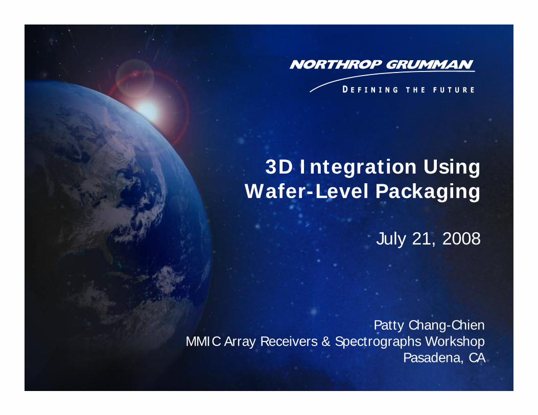
July 21, 2008
Patty Chang-ChienMMIC Array Receivers & Spectrographs Workshop
Pasadena, CA
3D Integration Using Wafer-Level Packaging
2
Agenda
• Wafer-Level Packaging Technology Overview
• IRAD development on large arrays
• Advanced Integration
• Next Level Assembly
• Summary / Future work
3
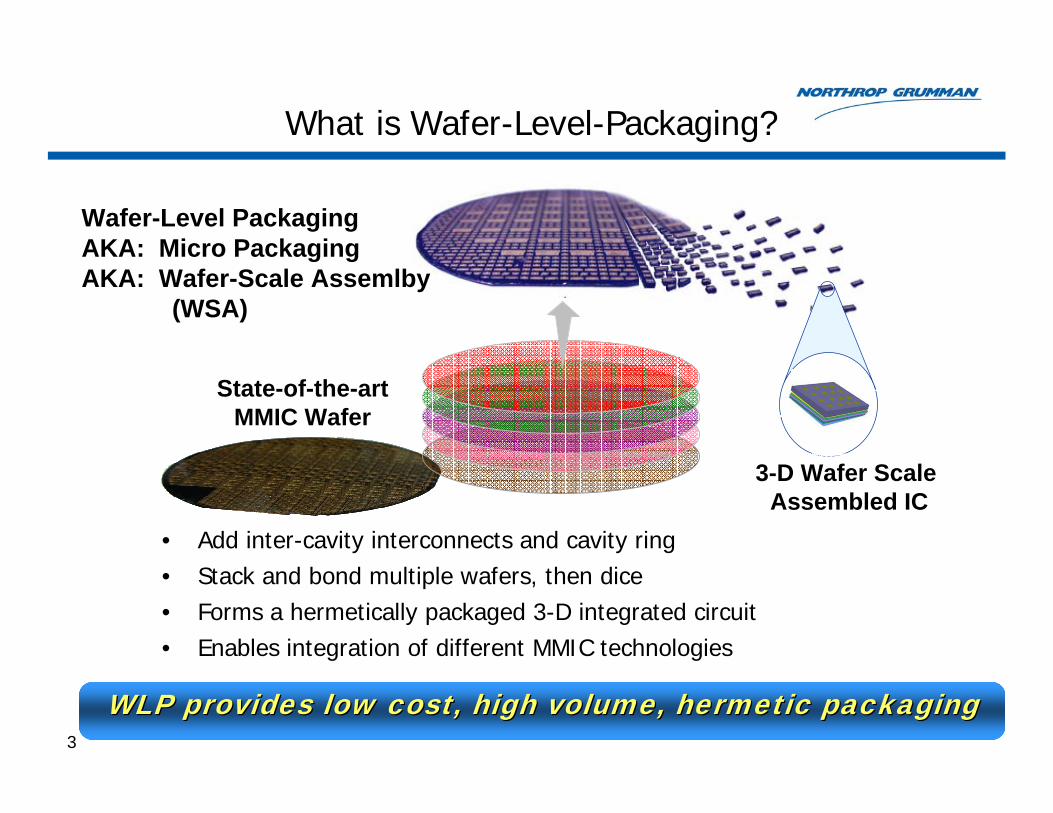
What is Wafer-Level-Packaging?
• Add inter-cavity interconnects and cavity ring• Stack and bond multiple wafers, then dice • Forms a hermetically packaged 3-D integrated circuit• Enables integration of different MMIC technologies
3-D Wafer Scale Assembled IC
State-of-the-artMMIC Wafer
Wafer-Level PackagingAKA: Micro PackagingAKA: Wafer-Scale Assemlby
(WSA)
WLP provides low cost, high volume, hermetic packagingWLP provides low cost, high volume, hermetic packaging
4
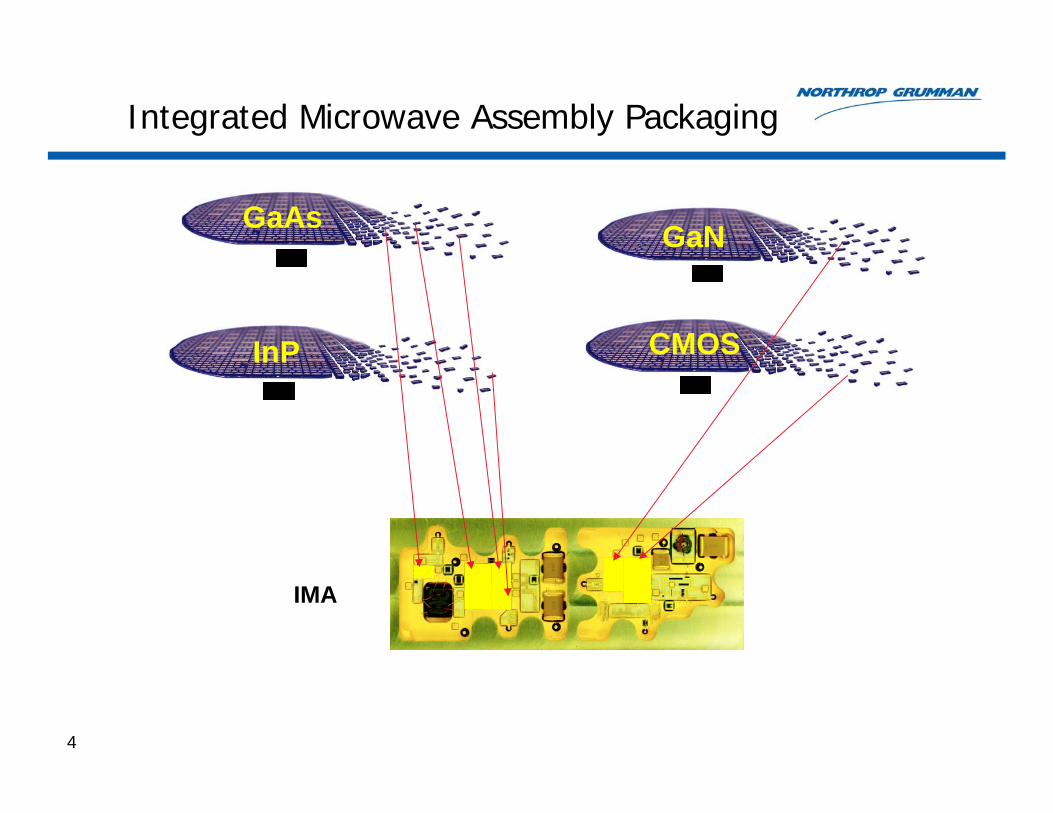
GaAs
InP
GaN
CMOS
Integrated Microwave Assembly Packaging
IMA
5
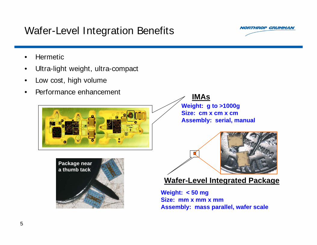
Wafer-Level Integration Benefits
• Hermetic
• Ultra-light weight, ultra-compact
• Low cost, high volume
• Performance enhancement IMAs
Wafer-Level Integrated PackageWeight: < 50 mgSize: mm x mm x mmAssembly: mass parallel, wafer scale
Weight: g to >1000gSize: cm x cm x cmAssembly: serial, manual
Package near a thumb tack
6
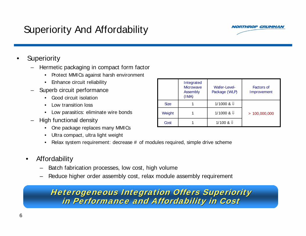
Superiority And Affordability
Heterogeneous Integration Offers SuperiorityHeterogeneous Integration Offers Superiorityin Performance and Affordability in Costin Performance and Affordability in Cost
> 100,000,000
Factors of Improvement
1/100 & ⇓1Cost
1/1000 & ⇓1Weight
1/1000 & ⇓1Size
Wafer-Level-Package (WLP)
Integrated Microwave Assembly (IMA)
• Superiority– Hermetic packaging in compact form factor
• Protect MMICs against harsh environment • Enhance circuit reliability
– Superb circuit performance• Good circuit isolation• Low transition loss• Low parasitics: eliminate wire bonds
– High functional density• One package replaces many MMICs• Ultra compact, ultra light weight• Relax system requirement: decrease # of modules required, simple drive scheme
• Affordability– Batch fabrication processes, low cost, high volume– Reduce higher order assembly cost, relax module assembly requirement
7
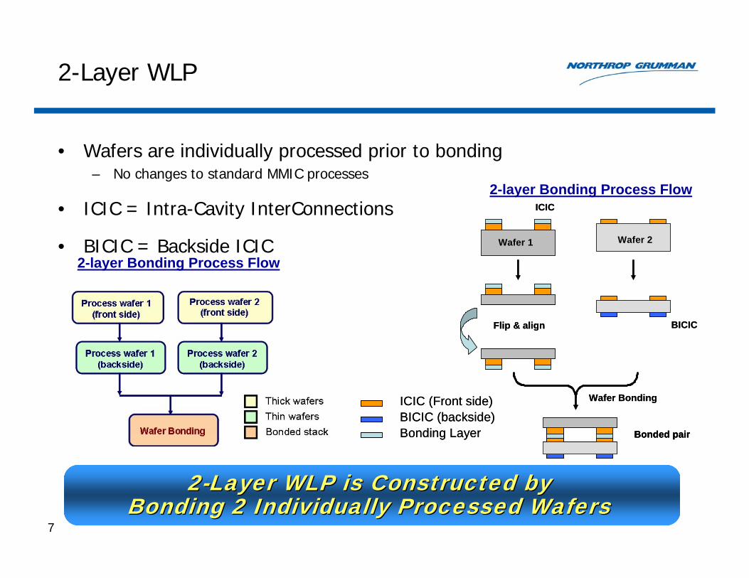
2-Layer WLP
BICIC
ICIC
Wafer 1 Wafer 2
Bonded pair
Flip & align
Wafer Bonding
BICIC
ICIC
Wafer 1 Wafer 2
Bonded pairBonded pair
Flip & align
Wafer Bonding
• Wafers are individually processed prior to bonding– No changes to standard MMIC processes
• ICIC = Intra-Cavity InterConnections
• BICIC = Backside ICIC
Bonding LayerBICIC (backside)ICIC (Front side)
Bonding LayerBICIC (backside)ICIC (Front side)
2-layer Bonding Process Flow
2-layer Bonding Process Flow
22--Layer WLP is Constructed by Layer WLP is Constructed by Bonding 2 Individually Processed Wafers Bonding 2 Individually Processed Wafers
8
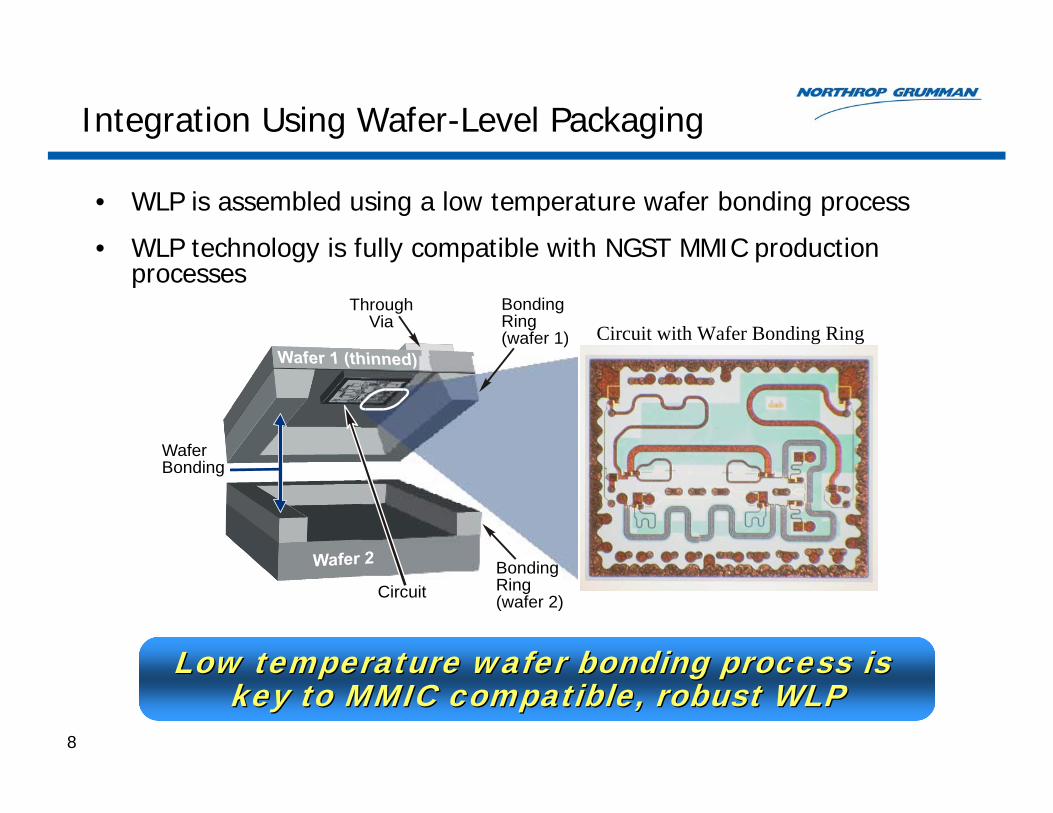
• WLP is assembled using a low temperature wafer bonding process
• WLP technology is fully compatible with NGST MMIC production processes
Low temperature wafer bonding process is Low temperature wafer bonding process is key to MMIC compatible, robust WLPkey to MMIC compatible, robust WLP
Integration Using Wafer-Level Packaging
Circuit with Wafer Bonding Ring Through
Via
Circuit(low-noise amplifier)
WaferBonding
BondingRing(wafer 1)
BondingRing(wafer 2)
9
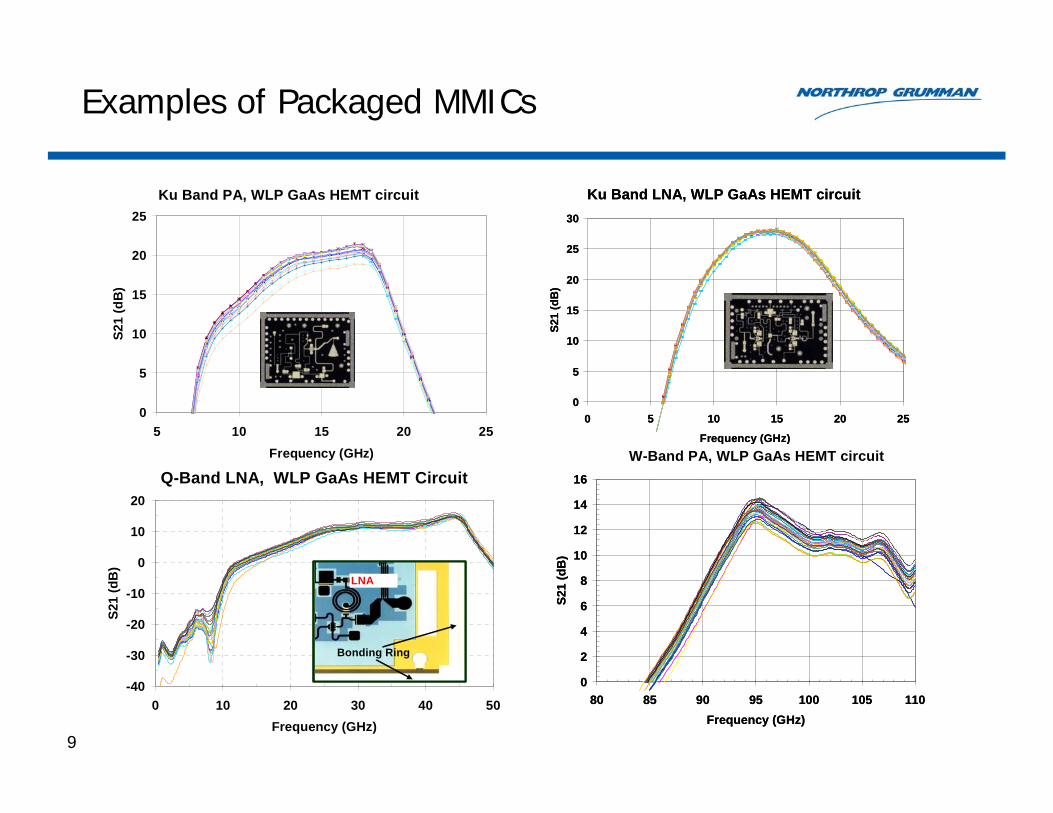
Examples of Packaged MMICs
0
5
10
15
20
25
30
0 5 10 15 20 25
Frequency (GHz)
S21
(dB
)
Ku Band LNA, WLP GaAs HEMT circuit
0
5
10
15
20
25
30
0 5 10 15 20 25
Frequency (GHz)
S21
(dB
)
Ku Band LNA, WLP GaAs HEMT circuit
0
5
10
15
20
25
5 10 15 20 25Frequency (GHz)
S21
(dB
)
Ku Band PA, WLP GaAs HEMT circuit
WLP Q-Band LNA (IRFFE)
-40
-30
-20
-10
0
10
20
0 10 20 30 40 50Frequency (GHz)
S21
(dB
)
LNA
Bonding Ring
LNA
Bonding Ring
Q-Band LNA, WLP GaAs HEMT Circuit
0
2
4
6
8
10
12
14
16
80 85 90 95 100 105 110Frequency (GHz)
S21
(dB
)
W-Band PA, WLP GaAs HEMT circuit
0
2
4
6
8
10
12
14
16
80 85 90 95 100 105 110Frequency (GHz)
S21
(dB
)
W-Band PA, WLP GaAs HEMT circuit
10
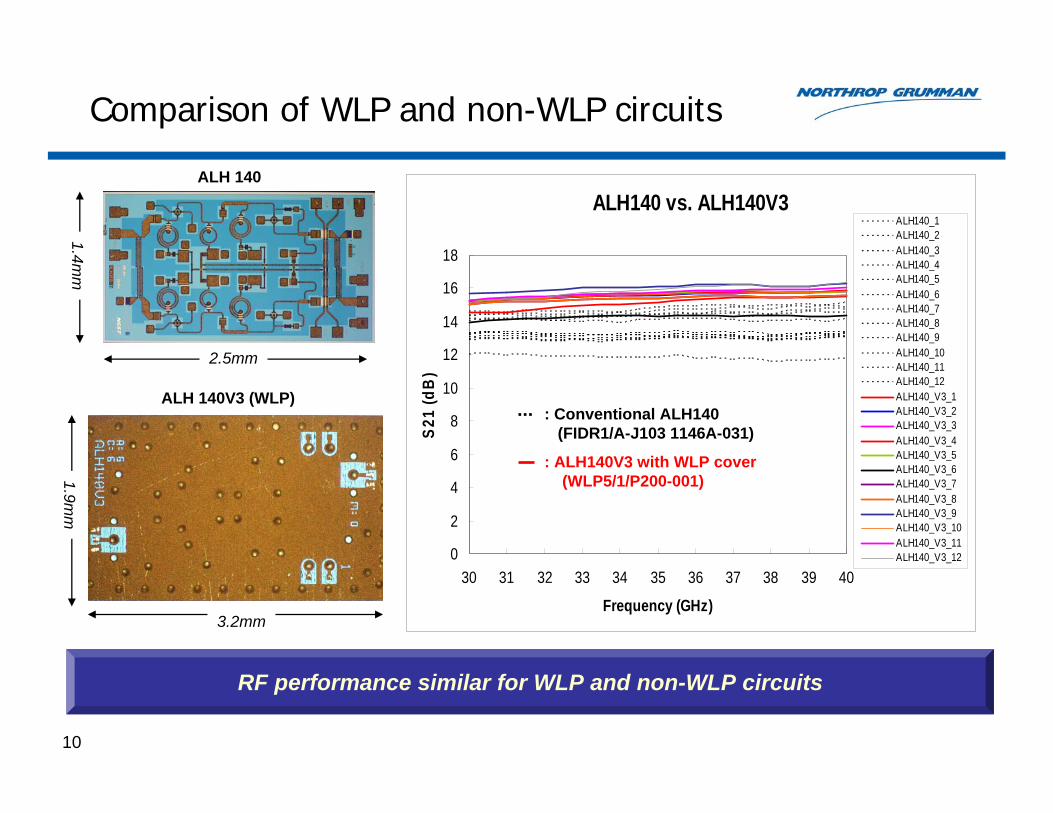
Comparison of WLP and non-WLP circuits
ALH140 vs. ALH140V3
0
2
4
6
8
10
12
14
16
18
30 31 32 33 34 35 36 37 38 39 40
Frequency (GHz)
S21
(dB
)
ALH140_1ALH140_2ALH140_3ALH140_4ALH140_5ALH140_6ALH140_7ALH140_8ALH140_9ALH140_10ALH140_11ALH140_12ALH140_V3_1ALH140_V3_2ALH140_V3_3ALH140_V3_4ALH140_V3_5ALH140_V3_6ALH140_V3_7ALH140_V3_8ALH140_V3_9ALH140_V3_10ALH140_V3_11ALH140_V3_12
: Conventional ALH140 (FIDR1/A-J103 1146A-031)
: ALH140V3 with WLP cover(WLP5/1/P200-001)
ALH 140
ALH 140V3 (WLP)
2.5mm
3.2mm
1.9mm
1.4mm
RF performance similar for WLP and non-WLP circuits
11
Converting Existing Chips to WLP
• Almost all existing chips can be converted into a WLP chip with a passive cover
• Layout changes are straightforward
• RF performance of converted chip will change depending on chip sensitivity, performance, and frequency
• Simulations may need to be performed to assess RF performance changes due to WLP cavity
• WLP conversion will generally increase the size of the chip
12
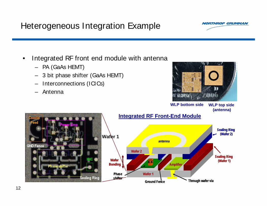
Heterogeneous Integration Example
• Integrated RF front end module with antenna– PA (GaAs HEMT)– 3 bit phase shifter (GaAs HEMT)– Interconnections (ICICs)– Antenna
WLP top side (antenna)
WLP bottom side
Wafer Bonding
Wafer 2
Wafer 1
Sealing Ring (Wafer 1)
Sealing Ring (Wafer 2)
Phaseshifter
Amplifier
Ground Fence Through wafer via
ICIC
antenna
Wafer Bonding
Wafer 2
Wafer 1
Sealing Ring (Wafer 1)
Sealing Ring (Wafer 2)
Phaseshifter
Amplifier
Ground Fence Through wafer via
ICIC
antenna
Integrated RF Front-End Module
Wafer 1
13
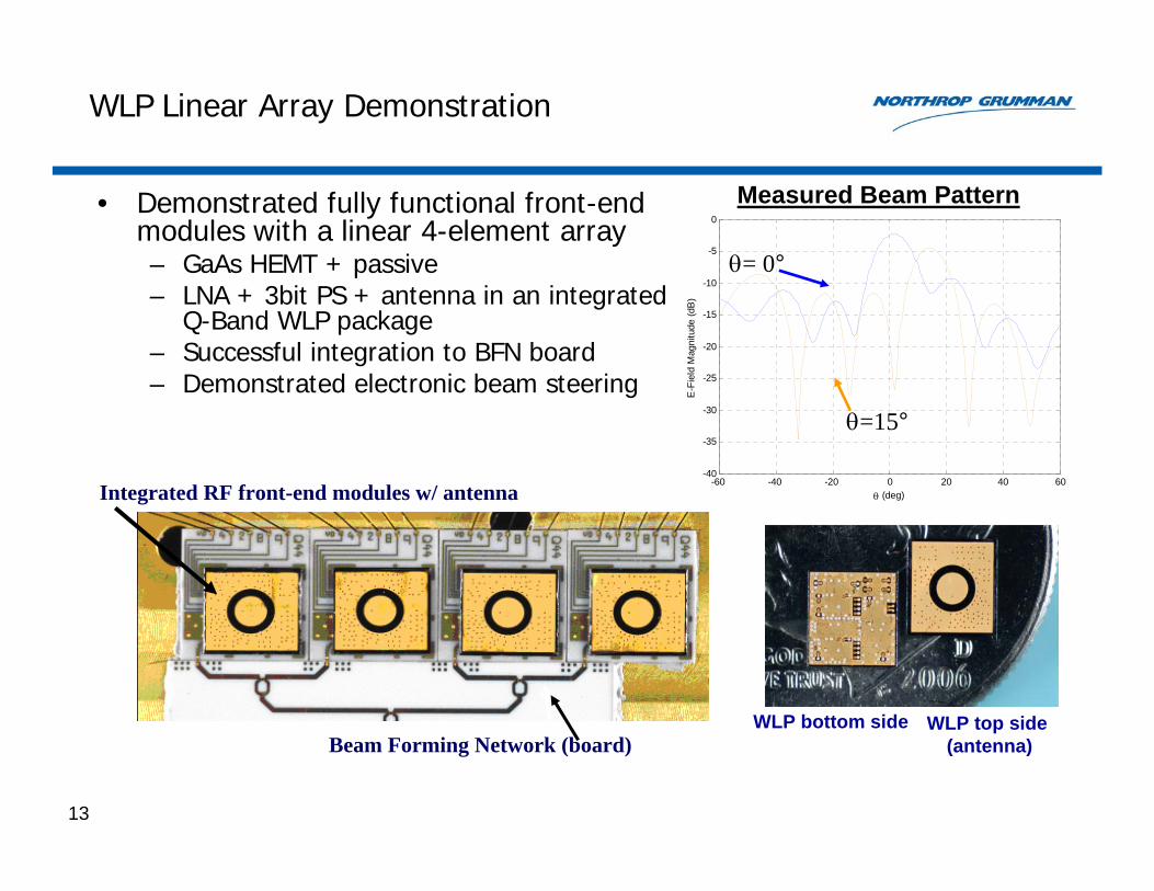
WLP Linear Array Demonstration
Beam Forming Network (board)
Integrated RF front-end modules w/ antenna
• Demonstrated fully functional front-end modules with a linear 4-element array– GaAs HEMT + passive – LNA + 3bit PS + antenna in an integrated
Q-Band WLP package– Successful integration to BFN board– Demonstrated electronic beam steering
-60 -40 -20 0 20 40 60-40
-35
-30
-25
-20
-15
-10
-5
0
θ (deg)
E-F
ield
Mag
nitu
de (d
B)
θ= 0°
θ=15°
Measured Beam Pattern
WLP top side (antenna)
WLP bottom side
14
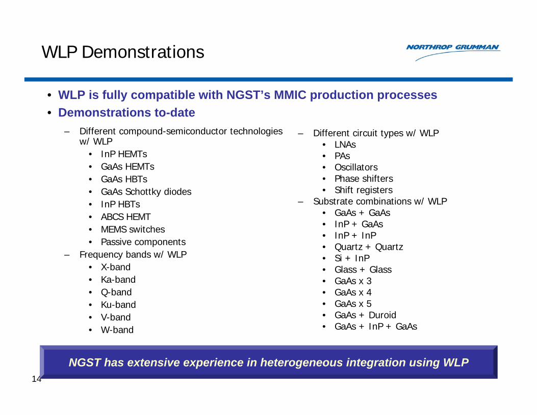
WLP Demonstrations
– Different compound-semiconductor technologies w/ WLP
• InP HEMTs• GaAs HEMTs• GaAs HBTs• GaAs Schottky diodes• InP HBTs• ABCS HEMT• MEMS switches• Passive components
– Frequency bands w/ WLP• X-band• Ka-band• Q-band• Ku-band• V-band• W-band
– Different circuit types w/ WLP• LNAs• PAs• Oscillators• Phase shifters• Shift registers
– Substrate combinations w/ WLP• GaAs + GaAs• InP + GaAs• InP + InP• Quartz + Quartz• Si + InP• Glass + Glass• GaAs x 3• GaAs x 4• GaAs x 5• GaAs + Duroid• GaAs + InP + GaAs
• WLP is fully compatible with NGST’s MMIC production processes• Demonstrations to-date
NGST has extensive experience in heterogeneous integration using WLP
15
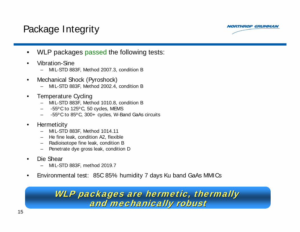
Package Integrity
WLP packages are hermetic, thermally WLP packages are hermetic, thermally and mechanically robustand mechanically robust
• WLP packages passed the following tests:• Vibration-Sine
– MIL-STD 883F, Method 2007.3, condition B
• Mechanical Shock (Pyroshock)– MIL-STD 883F, Method 2002.4, condition B
• Temperature Cycling– MIL-STD 883F, Method 1010.8, condition B– -55ºC to 125ºC, 50 cycles, MEMS– -55ºC to 85ºC, 300+ cycles, W-Band GaAs circuits
• Hermeticity– MIL-STD 883F, Method 1014.11– He fine leak, condition A2, flexible– Radioisotope fine leak, condition B– Penetrate dye gross leak, condition D
• Die Shear– MIL-STD 883F, method 2019.7
• Environmental test: 85C 85% humidity 7 days Ku band GaAs MMICs
16
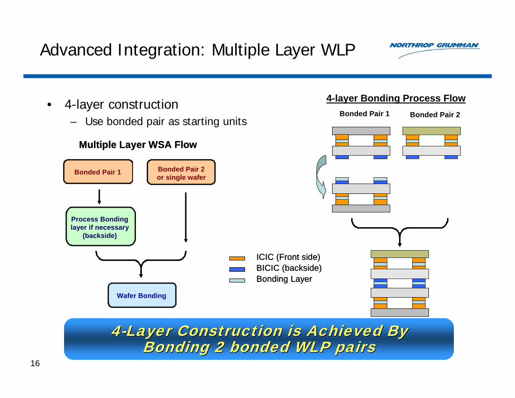
Advanced Integration: Multiple Layer WLP
Bonded Pair 1 Bonded Pair 2
Bonding LayerBICIC (backside)ICIC (Front side)
Bonding LayerBICIC (backside)ICIC (Front side)
4-layer Bonding Process Flow• 4-layer construction– Use bonded pair as starting units
Process Bonding layer if necessary
(backside)
Wafer Bonding
Bonded Pair 1 Bonded Pair 2 or single wafer
Multiple Layer WSA Flow
Process Bonding layer if necessary
(backside)
Wafer Bonding
Bonded Pair 1 Bonded Pair 2 or single wafer
Multiple Layer WSA Flow
44--Layer Construction is Achieved ByLayer Construction is Achieved ByBonding 2 bonded WLP pairsBonding 2 bonded WLP pairs
17
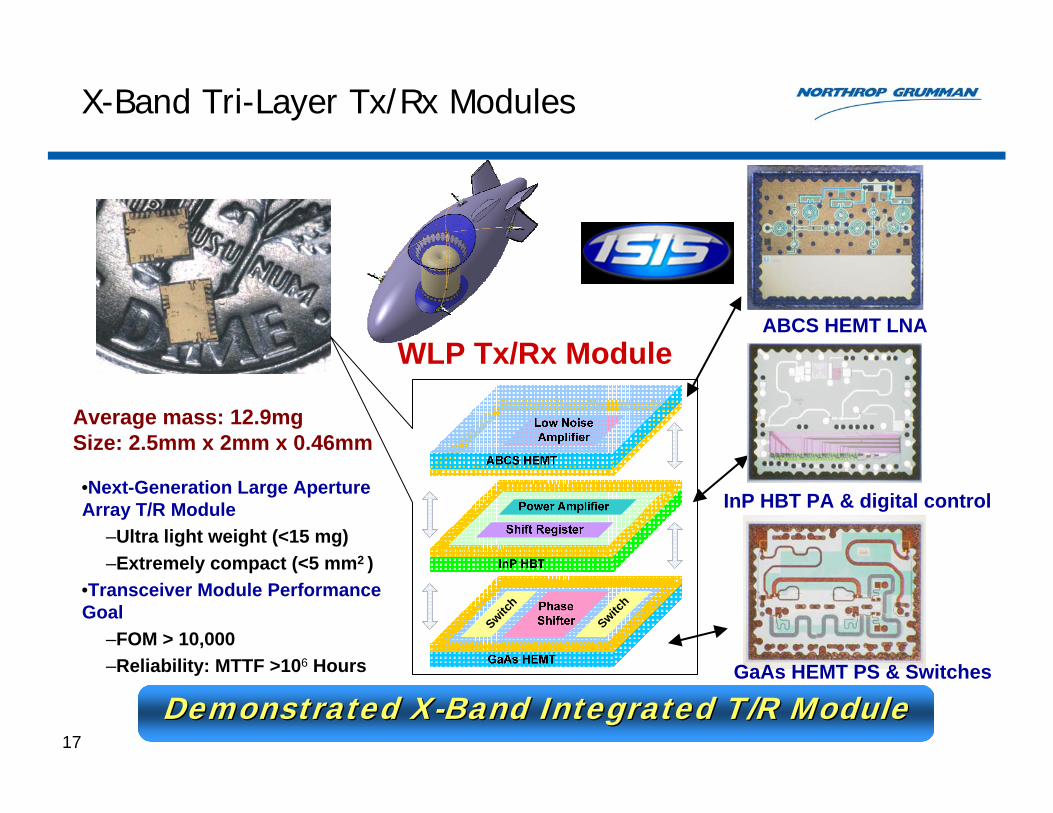
X-Band Tri-Layer Tx/Rx Modules
Switch
Switch
WLP Tx/Rx ModuleABCS HEMT LNA
InP HBT PA & digital control
GaAs HEMT PS & Switches
Demonstrated XDemonstrated X--Band Integrated T/R ModuleBand Integrated T/R Module
Average mass: 12.9mgSize: 2.5mm x 2mm x 0.46mm
•Next-Generation Large Aperture Array T/R Module
–Ultra light weight (<15 mg)–Extremely compact (<5 mm2 )
•Transceiver Module Performance Goal
–FOM > 10,000–Reliability: MTTF >106 Hours
18
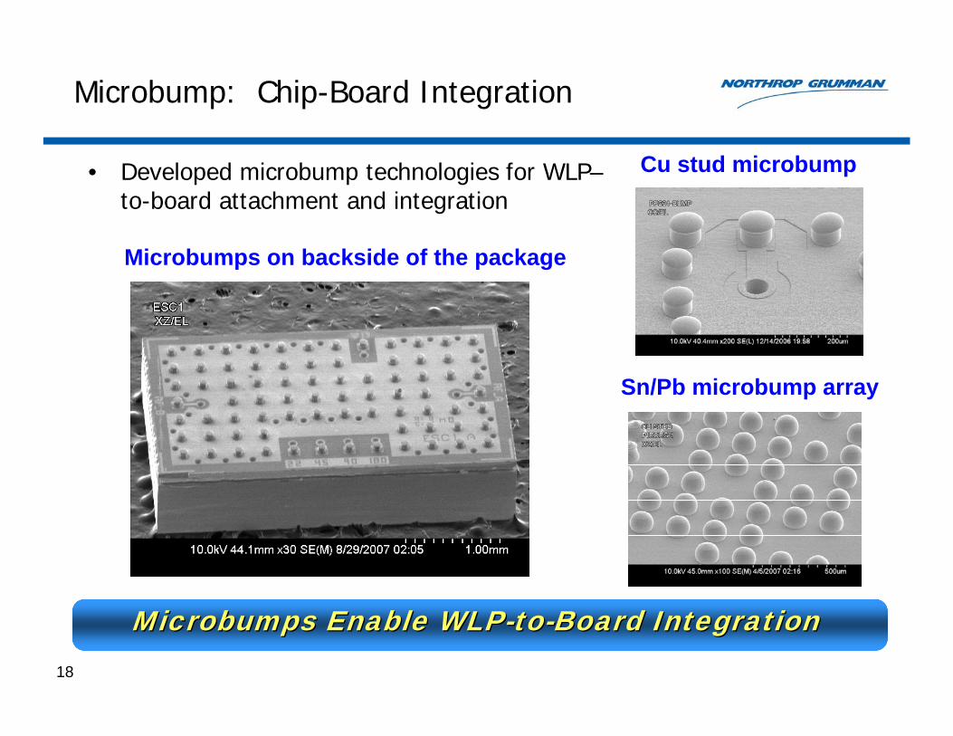
Microbump: Chip-Board Integration
• Developed microbump technologies for WLP–to-board attachment and integration
Sn/Pb microbump array
Cu stud microbump
MicrobumpsMicrobumps Enable WLPEnable WLP--toto--Board Integration Board Integration
Microbumps on backside of the package
19
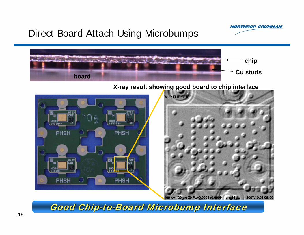
Direct Board Attach Using Microbumps
X-ray result showing good board to chip interfaceboard
chip
Cu studs
Good ChipGood Chip--toto--Board Board MicrobumpMicrobump InterfaceInterface
20
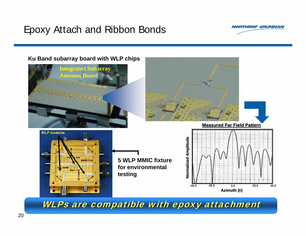
Epoxy Attach and Ribbon Bonds
Integrated Subarray Antenna Board
Ku Band subarray board with WLP chips
Azimuth (θ)N
orm
aliz
ed A
mpl
itude
0.0 25.0 45.0-25.0-45.0
Measured Far Field Pattern
Azimuth (θ)N
orm
aliz
ed A
mpl
itude
0.0 25.0 45.0-25.0-45.0
Measured Far Field Pattern
5 WLP MMIC fixture for environmental testing
WLPsWLPs are compatible with epoxy attachmentare compatible with epoxy attachment
21
Summary & Future Work
• Demonstrated 100% MMIC compatibility of WLP technology with MMICproduction processes– Many circuits using different semiconductor technology
• Demonstrated heterogeneous integration using WLP
• Demonstrated robust hermetic WLP packages
• Proven manufacturability (yield and performance)
• Long-term package reliability in progress
• Continue to develop/mature advanced integration technology
• Technology qualification in progress