EE 105 Semiconductors - University of California, Berkeley 105 Lecture 2: Semiconductors B. E. Boser...
29
B. E. Boser 1 EE 105 Semiconductors Bernhard E. Boser University of California, Berkeley [email protected] Copyright © 2012 by Bernhard Boser EE 105 Lecture 2: Semiconductors
Transcript of EE 105 Semiconductors - University of California, Berkeley 105 Lecture 2: Semiconductors B. E. Boser...
B. E. Boser 1
EE 105
Semiconductors
Bernhard E. Boser
University of California, Berkeley
Copyright © 2012 by Bernhard Boser
EE 105 Lecture 2: Semiconductors
B. E. Boser 2
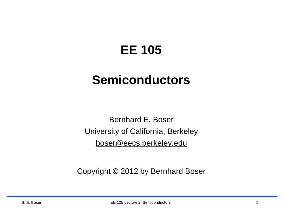
Active Devices
• Control (current) flow
• Cascadeable:
– Compatible inputs and outputs including
– Same physical domain, e.g.
• Electrical
• Pneumatic
• Chemical
• Mechanical
– Compatible signal levels, e.g.
• Switch with 5V control signal must be able to switch 5V at output
• Examples:
– Transistor
– Relays
– Vacuum tube
EE 105 Lecture 2: Semiconductors
B. E. Boser 3
Semiconductors
EE 105 Lecture 2: Semiconductors
B. E. Boser 4
Electrical Conduction
EE 105 Lecture 2: Semiconductors
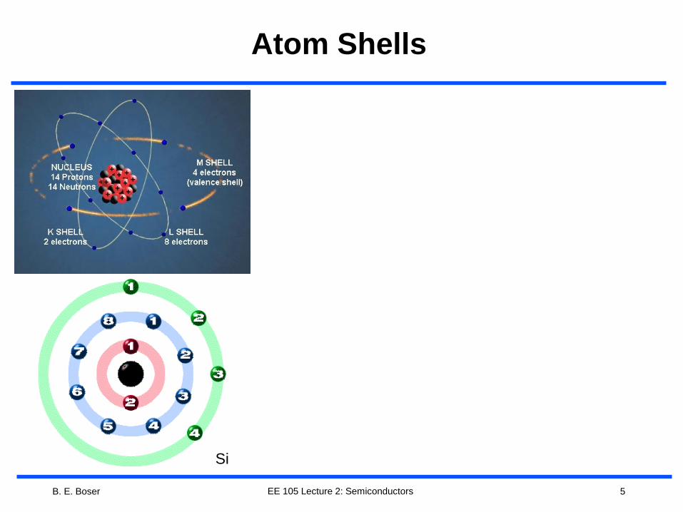
B. E. Boser 5
Atom Shells
EE 105 Lecture 2: Semiconductors
Si
B. E. Boser 6
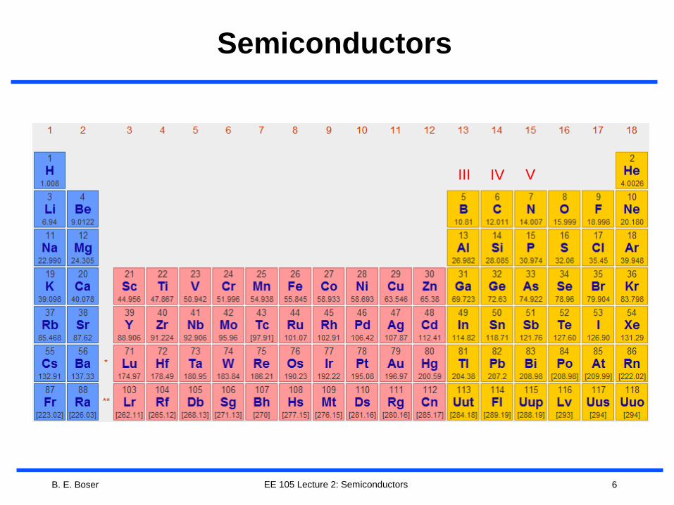
Semiconductors
EE 105 Lecture 2: Semiconductors
III IV V
B. E. Boser 7
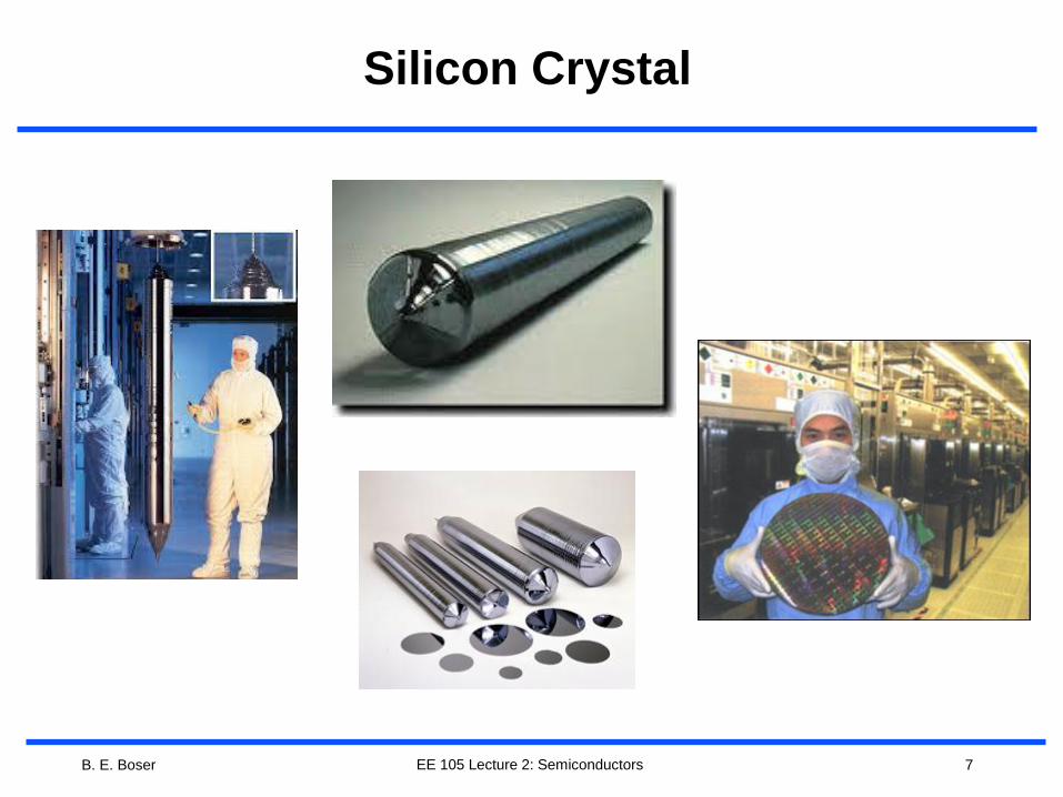
Silicon Crystal
EE 105 Lecture 2: Semiconductors
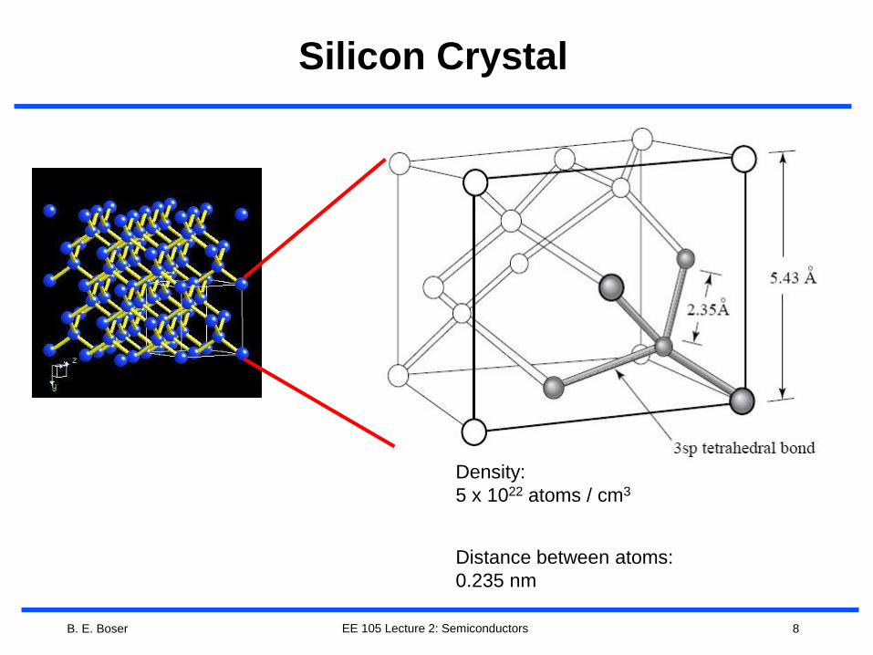
B. E. Boser 8
Silicon Crystal
EE 105 Lecture 2: Semiconductors
Density:
5 x 10²² atoms / cm3
Distance between atoms:
0.235 nm
B. E. Boser 9
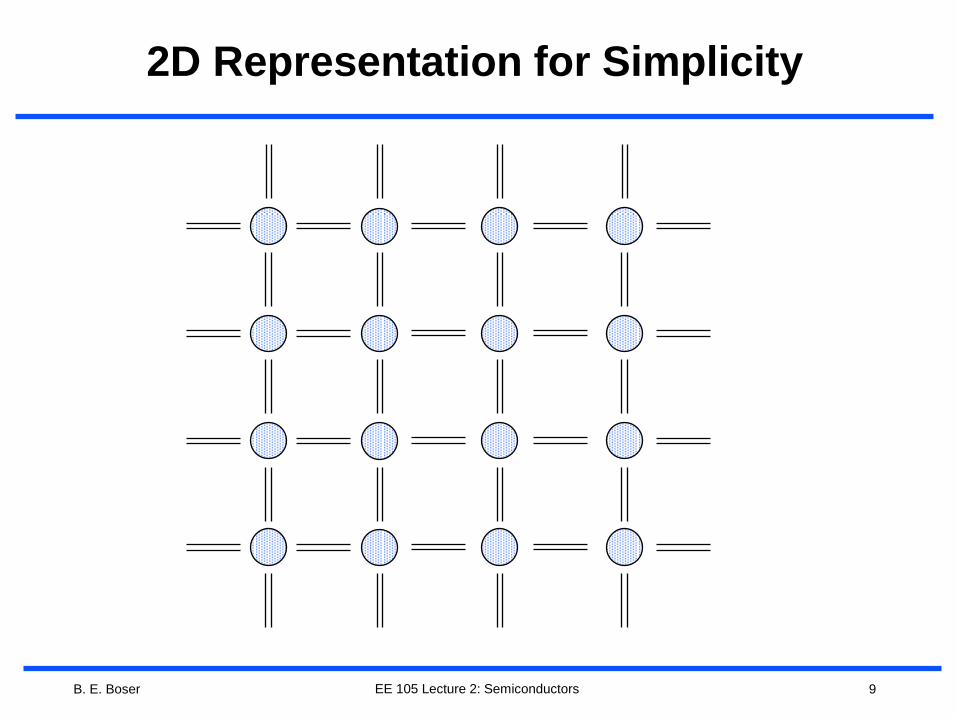
2D Representation for Simplicity
EE 105 Lecture 2: Semiconductors
B. E. Boser 10
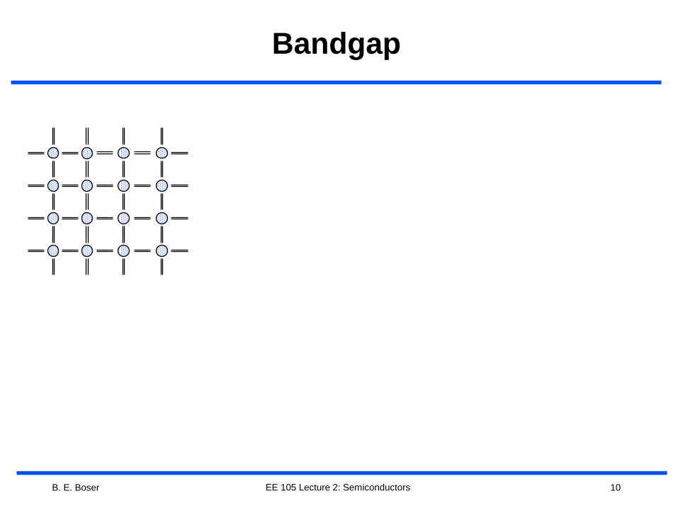
Bandgap
EE 105 Lecture 2: Semiconductors

B. E. Boser 11
Intrinsic Carrier Concentration ni
EE 105 Lecture 2: Semiconductors
40 20 0 20 40 60 801 10
6
1 107
1 108
1 109
1 1010
1 1011
1 1012
1012
106
n i T x T 0
cm3
8555 T x

B. E. Boser 12
Semiconductors Summary
EE 105 Lecture 2: Semiconductors
B. E. Boser 13
Drift Current
EE 105 Lecture 2: Semiconductors
B. E. Boser 14
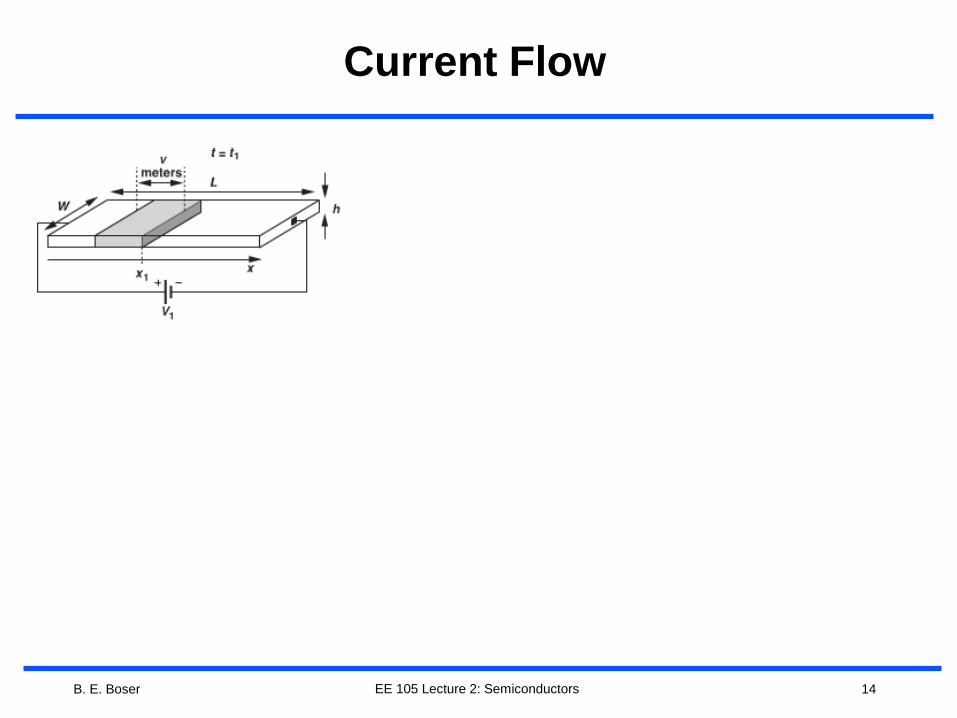
Current Flow
EE 105 Lecture 2: Semiconductors
B. E. Boser 15
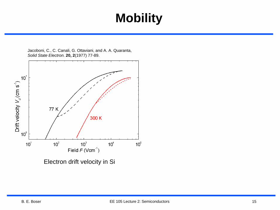
Mobility
EE 105 Lecture 2: Semiconductors
Electron drift velocity in Si
Jacoboni, C., C. Canali, G. Ottaviani, and A. A. Quaranta,
Solid State Electron. 20, 2(1977) 77-89.
B. E. Boser 16
Drift Current Example
EE 105 Lecture 2: Semiconductors
B. E. Boser 17
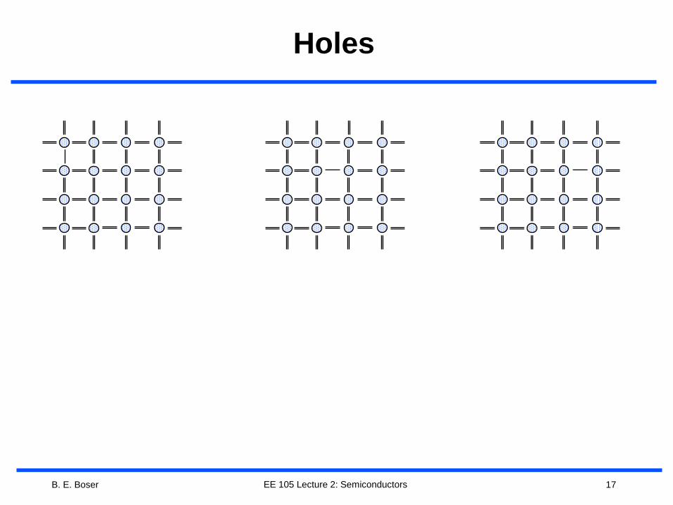
Holes
EE 105 Lecture 2: Semiconductors
B. E. Boser 18
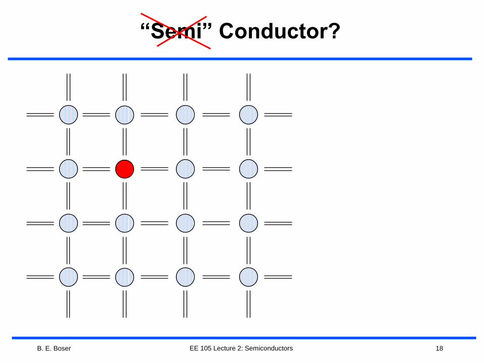
“Semi” Conductor?
EE 105 Lecture 2: Semiconductors
B. E. Boser 19
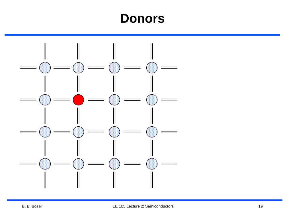
Donors
EE 105 Lecture 2: Semiconductors
B. E. Boser 20
Question
Is a doped semiconductor charge neutral?
EE 105 Lecture 2: Semiconductors
B. E. Boser 21
Uniform Semiconductors Summary
EE 105 Lecture 2: Semiconductors
B. E. Boser 22
pn Junction
(Diode)
EE 105 Lecture 2: Semiconductors
B. E. Boser 23
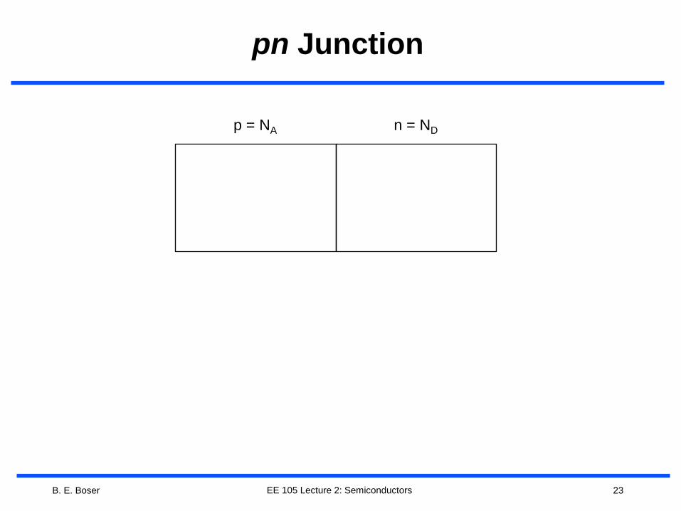
pn Junction
EE 105 Lecture 2: Semiconductors
n = ND p = NA
B. E. Boser 24
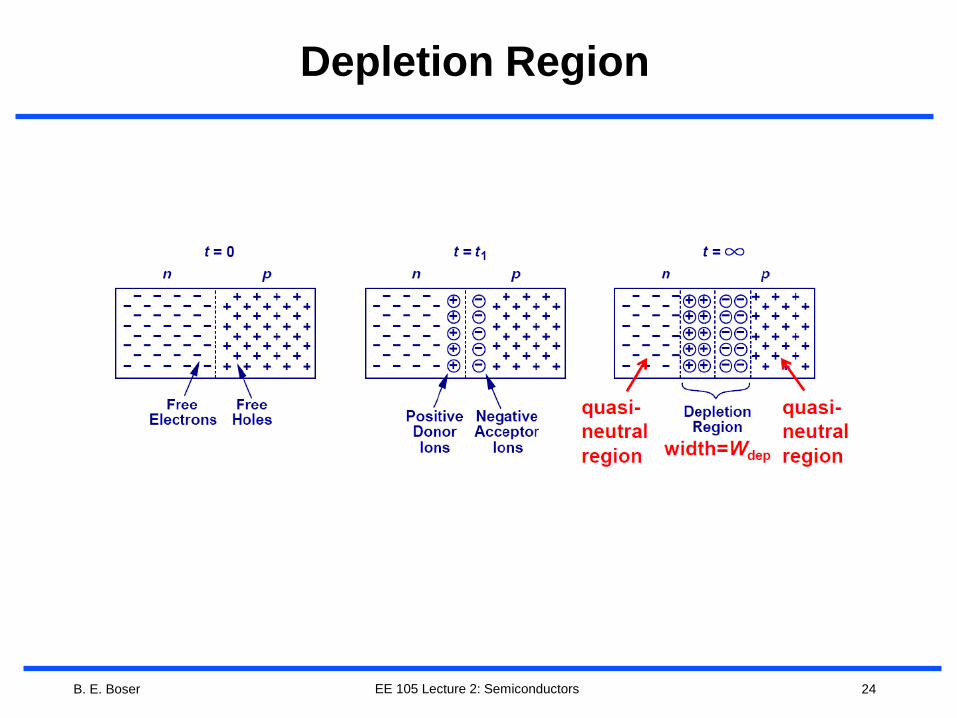
Depletion Region
EE 105 Lecture 2: Semiconductors
B. E. Boser 25
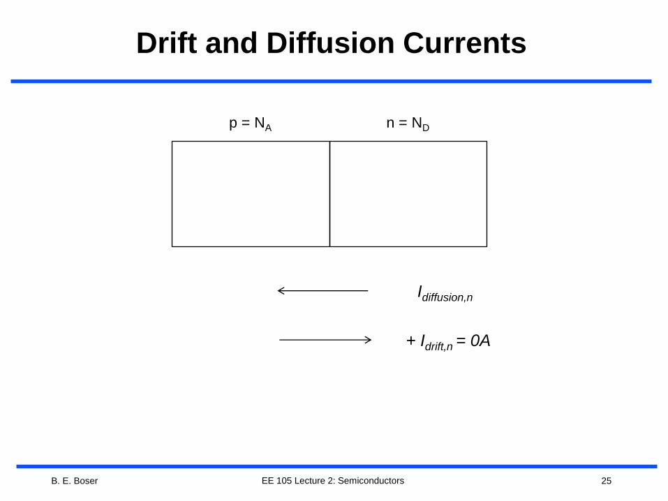
Drift and Diffusion Currents
EE 105 Lecture 2: Semiconductors
+ Idrift,n = 0A
Idiffusion,n
n = ND p = NA
B. E. Boser 26
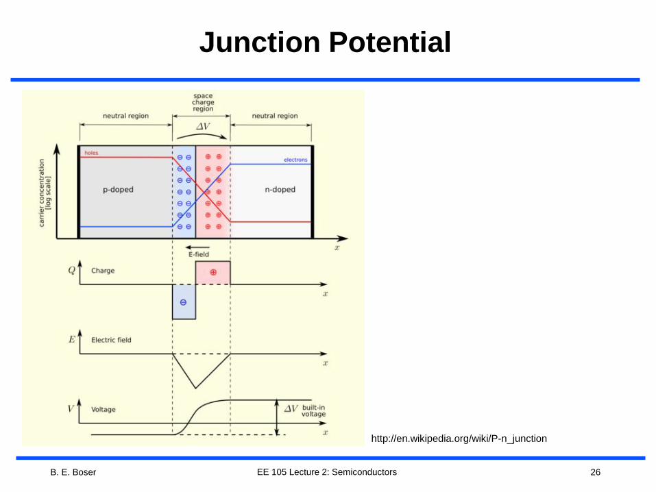
Junction Potential
EE 105 Lecture 2: Semiconductors
http://en.wikipedia.org/wiki/P-n_junction
B. E. Boser 27
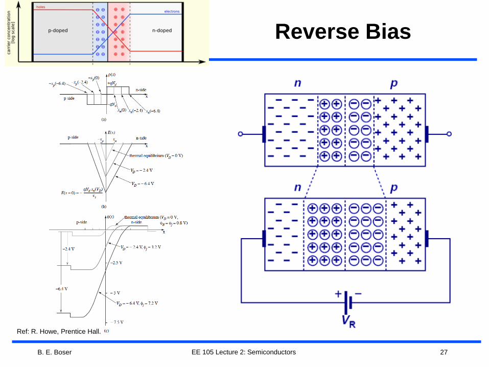
Reverse Bias
EE 105 Lecture 2: Semiconductors
Ref: R. Howe, Prentice Hall.

B. E. Boser 28
Forward Bias
EE 105 Lecture 2: Semiconductors
B. E. Boser 29
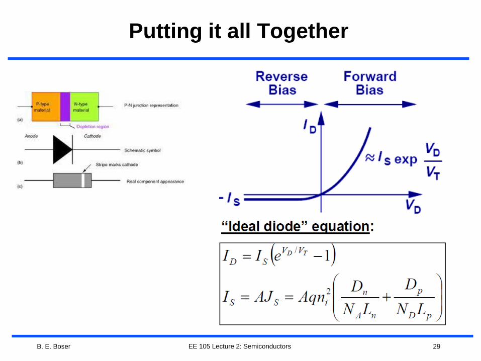
Putting it all Together
EE 105 Lecture 2: Semiconductors