Optical and Electrical Properties of Spray Pyrolysis Deposited Nano-crystalline BFO Films
Upload
nguyencongCategory
view
225download
0
THE JOHNS HOPKINS UNIVCftSITY
APPLIED PHYSICS LABORATORYSiLvcft SPUING. MARYLAND
OPTICAL INVESTIGATIONS OF'
NON-CRYSTALLINE SEMICONDUCTORS
FINAL TECHNICAL REPORT
Covering the period February 1, 1970 to January 31, 1973
-NASA"Gr-a'n-t~#NG-R-2-r=0'09-033-
Prepared by:
N. A. Blum
C. Feldman
K. Moorj ani
i'VJfen RECEIVED ' , ; ,
f ACIUT1 -:'=-'BRANCH
https://ntrs.nasa.gov/search.jsp?R=19750010023 2018-07-21T13:50:35+00:00Z
-1-
INTRODUCTION
This final technical report describes the results of
work performed at this Laboratory under NASA Grant
No. NGR-009-033. This Grant was one of the earliest Govern-
ment supported research projects in the area of amorphous semi-
.conductors. Until recently, solid state physics had been
concerned primarily with crystalline materials - a concern
which has led to a revolution in electronics technology.
The study of the fundamental properties of disordered semi-
conductors indicates that many of these properties responsible
for the huge technological success of crystalline materials
are still present in the disordered materials. In addition,
the disordered systems hold much promise for contributing their
own unique attributes to the development of semiconductor tech-
nology. For example, their insensitivity to structural changes,
wrought by exposure to hostile ambient conditions such as
temperature fluctuations and radiation fields, immediately
suggests their application to certain classes of hardened
devices". ~But, ~as~ih~the case" of crystalline semiconductor T
technology, the fundamental physical properites, materials
characterization and basic theory must establish a firm
foundation before there can be much chance of significant
technological advance.
During the two years covered by this report, we have
investigated the optical properties of carefully prepared
amorphous silicon and boron. Much has been learned about
characterizing these materials and measuring their purities.
The groundwork has been prepared for understanding the behavior
and properties of amorphous semiconductors and for the fabrica-
tion of useful devices based upon such an understanding. A
number of technical reports have appeared in the scientific
-2-
literature (see Appendix listing 6 references published with
NASA support) and a paper on the optical properties of amorphous
silicon and boron films is being prepared. Our work on dis-
ordered semiconductors has developed a firm foundation under
NASA sponsorship and further work is being continued under
alternate sponsorship.
This report covers three areas of investigation into the
properties of non-crystalline materials: (1) optical properties
of elemental amorphous semiconductors, (2) Mossbauer studies
of disordered systems, and (3) theoretical aspects of dis-
ordered semiconductors. These will be described briefly
below. Background material has been provided in the original
proposal . Detailed results of the completed work have been,
or will soon be, published. The detailed results which have
been published are attached to this report.
Optical Properties of Elemental Amorphous Semiconductors
Optical absorption studies of solids are a classic means
of determining fundamental properties of semiconductors such
as band gaps, density of states, and impurity levels. Optical
studies have, of course, accompanied and aided the development
of crystalline semiconducting devices. In the investigation
of amorphous materials, optical studies are playing a similar
role, but a great deal of controversy surrounds the inter-
pretation of the results. The sharpness of the band edge,
for example, is still not entirely resolved. Some investi-
gators have observed sharp band edges in amorphous germanium
and silicon, while others have observed tails. Band tailing
is expected according to the presently accepted theory of
disordered systems.
-3-
Optical studies in amorphous materials are somewhat
more difficult than similar studies on crystalline systems.
The samples investigated in this report are in the form of
thin films. There are problems associated with sample purity
during fabrication, substrate influence,. optical interference
effects, and surface contamination after the sample is removed
from the vacuum. Exploring the band tails in amorphous systems
also requires greater sensitivity and lower background than is
usually employed for normal crystal studies.
An optical apparatus was constructed to maintain the
sample purity and provide the sensitivity necessary to explore
the spectral absorption of amorphous materials. The optical
facility developed under the NASA Grant includes a double-beam
spectrometer for recording transmission spectra over a wide
range of sample environments. The instrument is extremely
versatile in that almost any combination of energy sources,
gratings, and detectors may be used to obtain spectra over
the range from 2000 A in the ultra-violet to 4/1 in the near
infra-red. The novel electronic detection scheme allows
-accurate tr-ansmittance—measurement s___to—be_jnade_ down__to__p_. JJJ
of the reference signal, while the SPEX Model 1400-11 double
grating spectrometer provides excellent spectral accuracy
and high resolution.
The complex refractive index for each sample was
determined by a computer analysis of the transmission versus
wavelength data for a pair of similarly prepared thin films
of different thicknesses. A computer program was developed
which properly takes into account the multiple reflections
between the thin amorphous film and the air as well as thosei
reflections between the substrate of known refractive index
(usually quartz) and the film on one side and air on the other.
Transmission data for two films identically prepared except
for thickness are analyzed to give the index of refraction n
and the absorption coefficient a for the amorphous film.
-4-
Preliminary results for silicon (Appendix I) and boron
films (Appendix II) have been presented at appropriate technical
symposia. A comprehensive summary of our findings is being
prepared for publication in a technical journal with copies
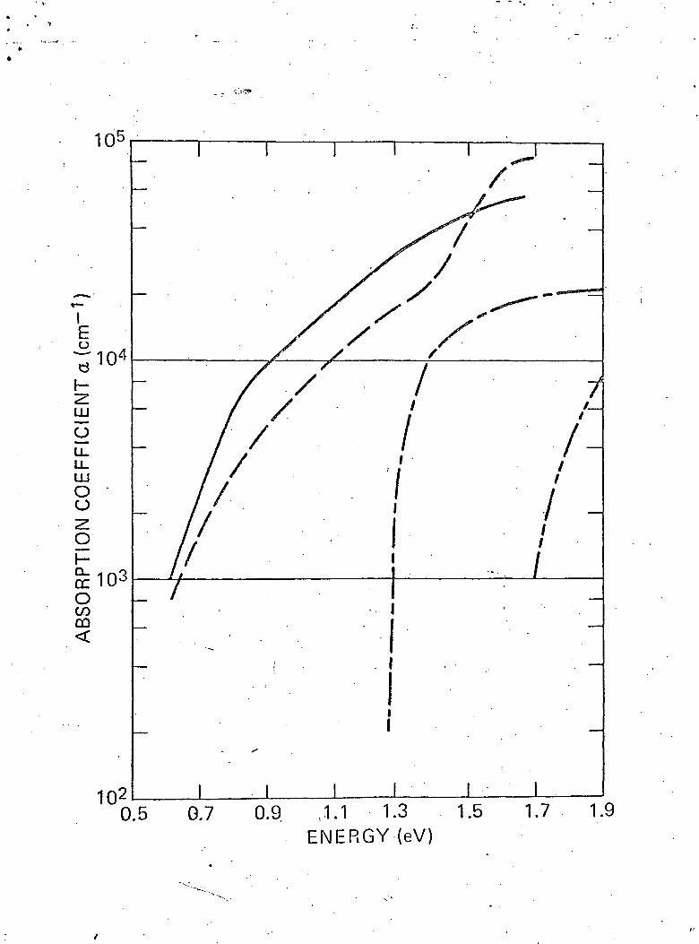
to be sent to NASA as an addendum to this report. Figure 1
shows the variation with photon energy of the refractive
index n and the absorption coefficient a for similarly
prepared amorphous and crystalline silicon films. These data
clearly show the presence of an absorptive tail in the amorphous
films and the absence of such a tail in the crystalline films.
The process of crystallization of amorphous films is not
well understood. We have investigated the crystallization
process in amorphous silicon films by observing optical
transmission changes in the films as they are heated at various
temperatures for different lengths of time. A model for
describing crystallization process was formulated and the
silicon film data fitted to the model. We believe the result
to be applicable to other systems as well as silicon. A
detailed report appears in the literature (see Appendix III).
In connection with the optical investigations sponsored
by NASA, we have for some time been concerned with the pre-
paration and analysis of ultra pure silicon films. The
technique of sputter-ion source mass analysis of the films
has been used to characterize the purity of the films and
as an aid in obtaining purer films. The technique is also
useful in determining bonding and clustering of atomic
neighbors in the films. This work has been described in(2)earlier Progress Memoranda to NASA v . A more detailed
account of this work, which was not supported by the NASA(3)Grant, has been published elsewhere v . The ultra pure
samples were, of course, used in the NASA optical study.
-5-
Mossbauer Studies of Disordered Systems
The Mossbauer technique has been established as a useful
method for investigating the microscopic structure of matter.
Its application to the study of disordered solids is outlined
in the proposal .
Under NASA sponsorship, the experimental apparatus was
acquired and tested. Efforts were made to design a system for
investigating amorphous tellurium films by Mossbauer
spectroscopy. The NASA program was terminated before any
satisfactory amorphous tellurium films could be obtained.
Recently we have, however, succeeded in preparing amorphous
tellurium films which give good Mossbauer spectra. There are
dramatic differences between the spectra of the amorphous and
crystallized samples. The experimental work and its interpreta-
tion are continuing at this Laboratory under alternate sponsor-
ship (AROD). Preliminary results indicate that, as we anticpated,
the Mossbauer technique is extremely sensitive to changes
in the structure of films.
Theoretical Aspects of Disordered Solids
Theoretical work, in collaboration with scientists from
other institutions, has centered on the extension of the single-
site Coherent Potential Approximation to include the effects of
scattering from pairs of sites and off-diagonal randomness. Both
weak and strong scattering cases have been analyzed. The numer-
ical results for the density of states have been obtained for
various disordered binary alloys. Detailed results have been
published and are included in Appendices IV, V and VI. The
model has also been applied to investigate the effect of
magnetic disorder on the spin wave spectrum and the curie tem-
perature of a randomly disordered spin-| Heisenberg ferromagnet.
In addition, computer programs for analyzing optical trans-
mission data were developed and modified for interpreting the
experiments performed on silicon and boron films.
-6-
REFERENCES
(1) "Proposal for Optical and Mossbauer Investigations
of Non-Crystalline Materials", Document #AD-4885,
The Johns Hopkins University, Applied Physics
Laboratory, October 9, 1970.
(2) "Progress Memoranda", The Johns Hopkins University,
Applied Physics Laboratory, PEG-002 (May 28, 1971)
and PEG-003 (January 17, 1972) under NASA Grant
No. NCR 21-009-033, Supplement #1.
(3) "The Study of Amorphous and Crystalline Silicon
Thin Films by Sputter-Ion Source Mass Spectroscopy"9 -
C. Feldman and F. G . Satkiewicz, Thin Solid Films
12, 217 (1972) and "Mass Spectra Analyses of
Impurities and Ion Clusters in Amorphous and
Crystalline Silicon Films", C. Feldman and F. G.
Satkiewicz, J. Electrochemical Soc., (to be
published in August 1973).
-7-
APPENDIX
Papers Published Citing Support under
NASA Grant No. NGR 21-009-033
I. "Optical Properties of Amorphous Silicon Films,
N. A. Blum, C. Feldman and K. Moorjani, Bull. Am.
Phys. Soc. 17, 114 (1972).
II. "Mass Spectrometry, Optical Absorption and Electrical
Properties of Amorphous Boron Films", C. Feldman, K. Moorjani
and N. A. Blum, Proc. Intl. Symposium on Boron, 1973
(to be published).
III. "The Crystallization of Amorphous Silicon Films",
N. A. Blum and C. Feldman, J. Non-Crystalline Solids
11, 242 (1972).
IV. "Pair Approximation in the Coherent Potential Theory of
Off-Diagonal Randomness", K. Moorjani, T.JTanaka and _.
S. M. Bose, Conduction in Low-Mobility Materials, Ed.
N. Klein, D. S. Tannhauser and M. Pollak (Taylor and Francis
Ltd., London 1971), pp. 167-173.
V. "Coherent Potential Theory of Off-Diagonal Randomness:
Binary Alloy", T. Tanaka, M. M. Sokoloski, K. Moorjani and
S. M. Bose, J. Non-Crystalline Solids 8-10 155 (1972)
VI. "Coherent Potential Theory of a Random Binary Alloy:
j Effects of Scattering from Two-Sites Clusters and Off-
Diagonal Randomness", K. Moorjani, T. Tanaka, M. M. Sokoloski
and S. M. Bose (submitted for publication).
Appendix I
Abstract submitted for the Annual Meeting of
The American Physical Society, January 31-February 3, 1972
Published in Bull. Am. Phys. Soc. 17, 114 (1972)
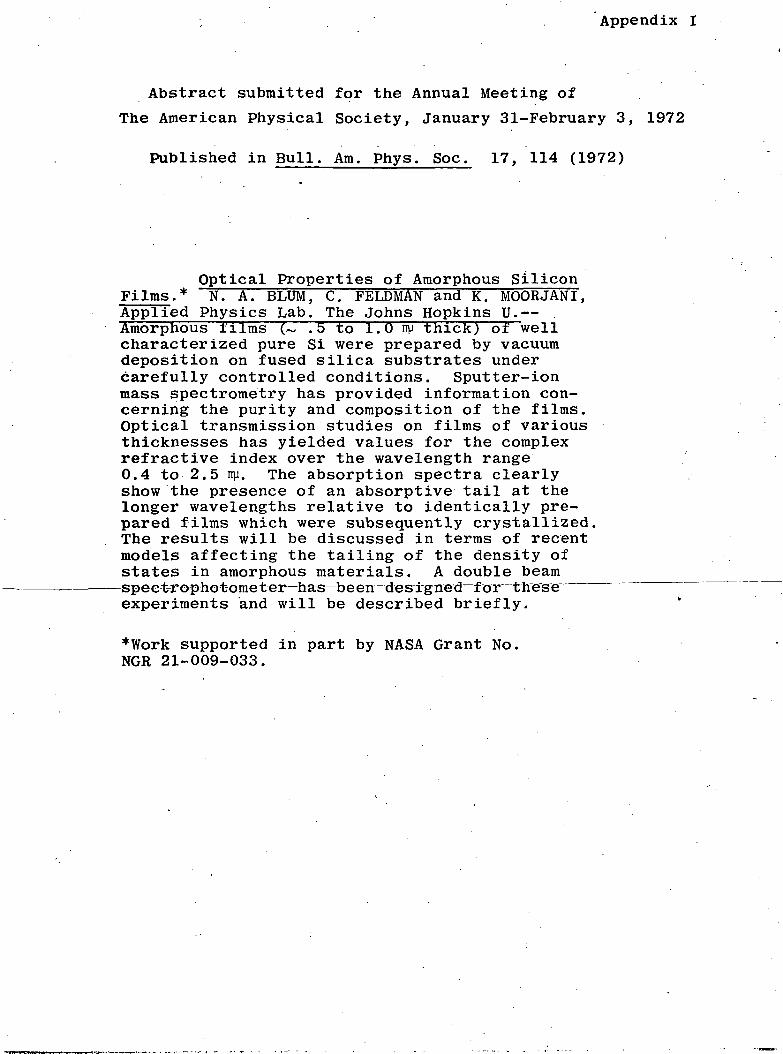
Optical Properties of Amorphous SiliconFilms.* N. A. BLUM, C. FELDMAN and K. MOORJANI,Applied Physics Lab. The Johns Hopkins U.— .Amorphous films (~ .5 to 1.0 ny thick) of wellcharacterized pure Si were prepared by vacuumdeposition on fused silica substrates undercarefully controlled conditions. Sputter-ionmass spectrometry has provided information con-cerning the purity and composition of the films.Optical transmission studies on films of variousthicknesses has yielded values for the complexrefractive index over the wavelength range0.4 to 2.5 n\i. The absorption spectra clearlyshow the presence of an absorptive tail at thelonger wavelengths relative to identically pre-pared films which were subsequently crystallized,The results will be discussed in terms of recentmodels affecting the tailing of the density ofstates in amorphous materials. A double beam-spee-t-rop-ho-t-omet-er—has—been—designed—for theseexperiments and will be described briefly.
*Work supported in part by NASA Grant No.NCR 21-009-033.
/ JE
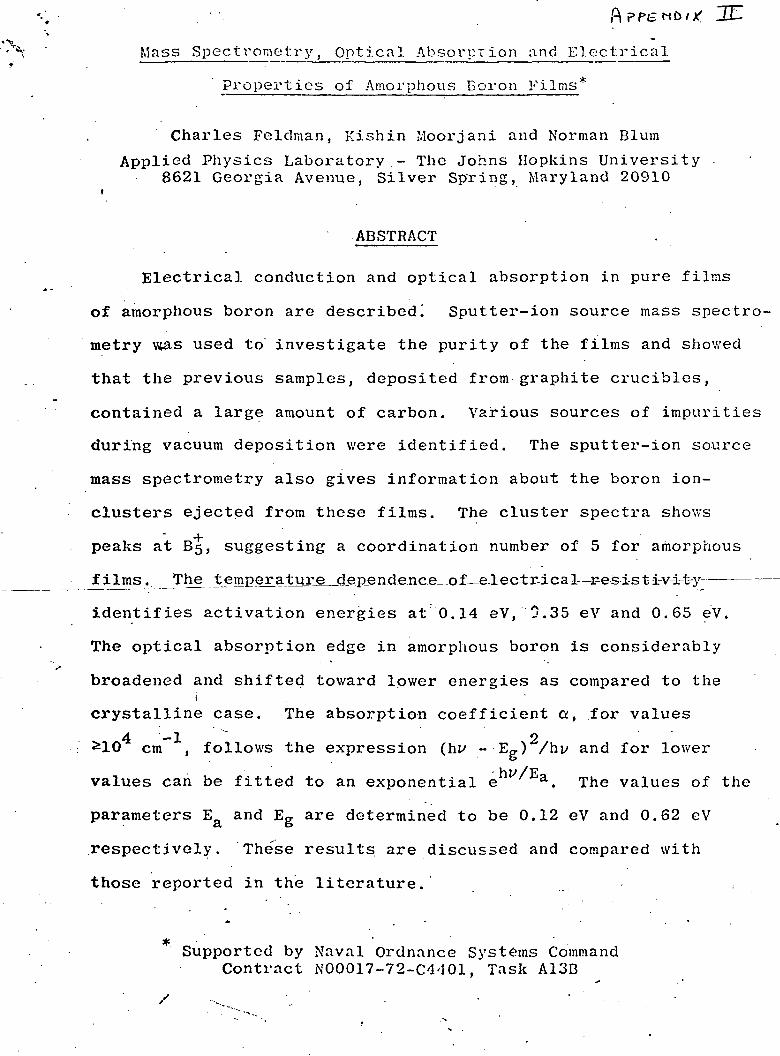
Mas s S p ectrometry, Optical Absorption and Electrical
Properties of Amorphous Boron Films*
Charles Feldman, Kishin Moorjani and Norman Blum
Applied Physics Laboratory.- The Johns Hopkins University8621 Georgia Avenue, Silver Spring, Maryland 20910
i
ABSTRACT
Electrical conduction and optical absorption in pure films
of amorphous boron are described! Sputter-ion source mass spectro-
metry was used to investigate the purity of the films and showed
that the previous samples, deposited from graphite crucibles,
contained a large amount of carbon. Various sources of impurities
during vacuum deposition were identified. The sputter-ion source
mass spectrometry also gives information about the boron ion-
clusters ejected from these films. The cluster spectra shows
peaks at 65, suggesting a coordination number of 5 for amorphous
films. The t^mpe^a_ture__de.p_endence_-of—eJectr-ical—r-esi-s-t-i-vi-t-y
identifies activation energies at 0.14 eV, 0.35 eV and 0.65 eV.
The optical absorption edge in amorphous boron is considerably
broadened and shifted toward lower energies as compared to thei .
crystalline case. The absorption coefficient a, .for values
4 - 1 2^10 cm , follows the expression (hf - Eg) /hi/ and for lower
values can be fitted to an exponential e a. The values of the
parameters E& and Eg are determined to be 0.12 eV and 0.62 eV
respectively. The'se results are discussed and compared with
those reported in the literature.
Supported by Naval Ordnance Systems CommandContract N00017-72-C4401, Task A13B
I. Introduction
Efforts since the previous Boron Conference have been
'concentrated on the improvement and refinement of techniques for
producing thin films. Refinements have been made in vacuum tech-
niques for producing the films and in optical techniques for
measuring their optical properties. A sputter-ion source mass
spectrometer has been used to analyze the films from the stand-
point of purity and ion clusters, and this information has beenc.
. • Iused to improve the purity of the films. The methods for pro-
ducing purer films and the conditions during vacuum deposition
are" described in the next section. The purity of these samples
as determined by sputter-ion source mass analysis is discussed in
Section III. It is found that the films described in previous
reports contain large amounts of carbon. Section IV deals with
the analysis of boron ion clusters in amorphous films as well as
in the bulk material. The electrical conduction and the optical
absorption in the purer samples are discussed and compared with
earlier results in Sections V and VI respectively. Finally, the
last section contains some concluding remarks on the present
findings.
I ' ' . . ' • ' '
II. Film Preparation
Samples were deposited in a 12" water-cooled stainless steel
vacuum bell jar. The system was evacuated by means of a mechanical
pump, an oil diffusion pump and a titanium getter pump. Appropriate
zeolite and liquid nitrogen traps are included in the system. The
-9pre-deposition pressure was less than 5 x 10 torr. Deposition
—8 —7pressures were between 7 x 10~ and 1 x 10~ torr. The deposition
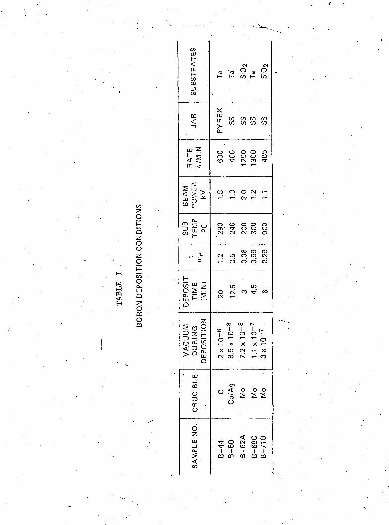
parameters for the samples described here are given in Table I.
Sample B-44 was deposited in a carbon crucible at a pressure of
—fi2 x 10 in a similar manner to that described in the previous
Conference. . An analysis of this film, to be discussed later,
showed that it contained a large quantity of carbon•. Sample B-66
was deposited from a silver-plated copper, water-cooled crucible,
and Sample B-62 and subsequent films used water-cooled stainless
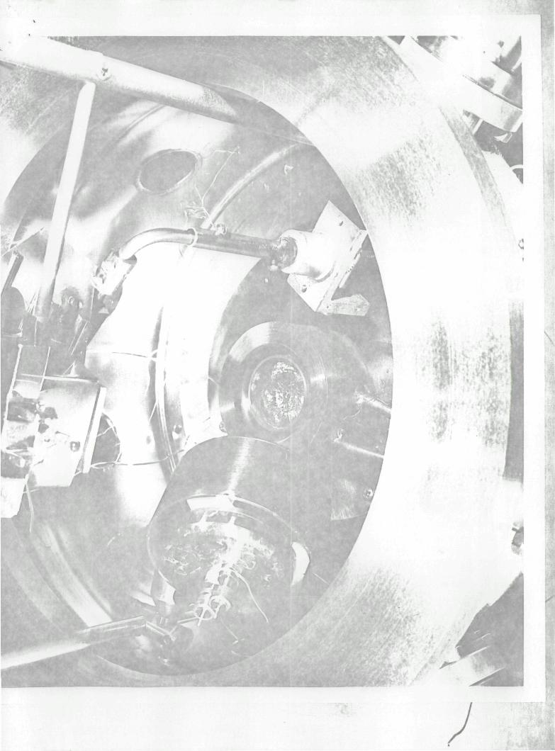
steel crucibles with molybdenum liners. A photograph of this
crucible and arrangement in the system is shown in Fig. 1. The
large diameter (3.5 cm) of the source allowed one to obtain a
fast deposition rate. The elimination, of the carbon crucible
brought about a lowering of the pressure during deposition since
the outgassing of the graphite crucible was difficult to eliminate.
Substrate temperatures between 100°C and 300°C represented the
maximum temperature recorded by a thermocouple in contact with the
back of a substrate during the deposition. Except when noted, the
heating of the substrate was due to radiation from the crucible.
In Samples 62 and 68, effort was made to deposit at high rates in
order to limit the occlusion of residual gases. The residual
atmosphere in the vacuum chamber was monitored with a mass
analyzer. Typical partial pressures of major gases are shown in
Table II. .
Bulk boron was obtained from United States Mineral Company
with the quoted purity of 99.99995. Attempts to crystallize the
boron films by.heating the samples in argon following the deposi-
tion have been unsuccessful. The films tend to crack and flake
-3-
off their substrate as they are crystallizing. Films deposited on
substrates maintained at 900°C remain, however, continuous and
smooth. The X-ray diffraction pattern of these films still shows
diffuse rings.
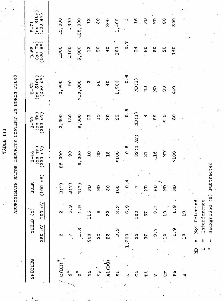
III. Sputter-ion Source Mass Analysis
The films were analyzed by means of a sputter-ion source
mass spectrometer . This spectrometer employs a 10 kev argon ion
beam which bombards the boron film, ejecting boron ions, boron ion
clusters, ion complexes, and impurity ions from the film. The
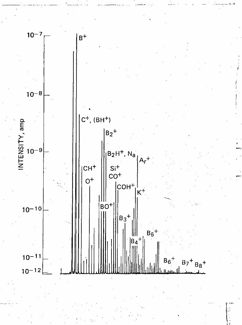
ejected ions are analyzed in a mass spectrometer. A typical
mass spectrometer trace is shown in Fig. 2. The analysis of boron
samples is very similar to that recently reported for silicon
(2)films . Impurity analysis was carried out using an energy
window of 100 eV and 250 eV. This allowed determination of atomic
impurities without interference from clusters and complexes.
The impurity analysis of the films is obtained from the
-mass—spectra~by-means—of~tfre~foTl~c>wi"n'g~"a"ppr^ximarte e quaTTicTnl
V
v y YB+
where the I's represent ion contents, and Y's the relative ion
yield. A knowledge of sputtering yields is thus essential for the
determination of impurity content. Yields based on elements in
elemental form are given in Table III, along with impurity analysis
of the samples listed in Table I. If the impurities are assumed
GCA Ion Microphobe Analytical Mass Spectrometer (IMS 101B),GCA Corp., Bedford, Mass.
-4- '•
to be in the oxidized state, the impurity content would be 10 -
15 times less.
The high content of carbon in Sample l?-44 is clearly due to
the graphite crucible. This is in contrns~ to statements found in
the literature that the vapor pressure of carbon is much lower
than that of boron at the melting point nine consequently one does
(3)not expect many carbon impurities in the '~:cron film v . The 8%
carbon impurity in Sample 44 is considerably greater than the
0.2% equilibrium solubility of carbon in cr_lk boron. If the
sample were crystallized, the carbon would probably reside on the
(4)grain boundaries as a separate C or B>C par-ise . Major impurities
in the films (see B-68) tend to be silicon and iron. As can be
seen from the tables, silicon may arrive fr ora the source itself.
The source of iron is more difficult to ce ~ermine. Analysis of
a different piece of bulk boron showed an :_ron contamination in
small areas on the surface. The high sili.ron, oxygen, carbon and
iron content of B-62A probably represents ~iie Si02 showing through
in pinholes as these impurities do not ap-^ar to the same extent
in samples deposited on tantalum substrat=r=. A direct comparison
between series B-68 deposited on Si00 (no- shown here) and on«
tantalum bears this out. Sample B-71 was deposited on a substrate
held at 900°C. In this sample the silicon and iron as well as
carbon and aluminum probably comes from ci.~"fusion from the sub-
strate into the film. The fused silica 5v..:- = trate contains carbon
and iron impurities as determined by the ~:.i~e mass analysis
techniques. Care was taken during this hi.rh temperature run to
-5-
avoid heating any stainless steel since it had been shown that
iron and chromium vapor could contaminate a sample at 900°C .
The samples do not appear to be contaminated with molybdenum
or silver from the deposition crucible.
The carbon and oxygen impurities in all samples are difficult
to analyze since there appears to be a surface reaction with the
sample during sputtering in the mass analysis procedure. The
carbon and oxygen impurity content in silicon films deposited by
the same technique and at somewhat higher pressures are considerably
less. McElligott and Roberts have demonstrated that O0 and CO£ I
are chemisorbed strongly on a deposited boron film and this
(5)chemisorption appears to be greater than on silicon surfaces
The amount of oxygen and carbon occluded in the films during
deposition can not account for the large quantity of C and 0
observed. Table II shows the calculated values of the ratio of'r\
gas molecules striking the substrate/cm /sec,(v ), to the borongas2
atoms striking the surface/cm /sec,( B). If all these gas
_mo.le.cules_stick-,—which—i-s—un-1-i-ke-l-y-T—t-he—sum—of the—oxygert b~eari"ng
species, assuming COo and 03 do not decompose, would give 434 ppm
oxygen impurity in Sample B-6S, while the mass analysis shows a
6000 ppm in Table III. The figures for O, C and perhaps N are
thus too high.
IV. Boron Ion Cluster Analysis
The mass spectra shown in Fig. 2 show peaks corresponding to
B~2 • . . Bg. The peaks 03 to Bg have not been observed in the mass
-6-
spectra when a thermal source rather than sputter source is used 'b'
The cluster peaks are complicated by the existence of two isotopes
of nlmost equal intensity. A cluster of three boron atoms, for
example, shows mass peaks at 30, 31, 32 and 33. The analysis of
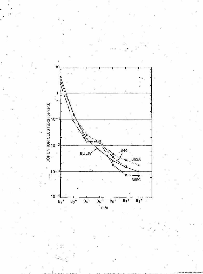
the clusters was accomplished by converting all peaks to an
average main cluster lln+ peak through the prediction of relativen
intensities. The results are shown in Fig. 3, which shows the
relative distribution of ion clusters ejected from the boron
target. Note the deviations in the films from the relatively
smooth distribution at B"£, which represents a cluster of 5 borono
atoms. In the case of previously studied silicon films, the
Si^ ion deviated from the smooth distribution ' . Using argu-
ments discussed previously for silicon, and assuming that the
distribution is related to short range order, one would draw the
conclusion from these curves that the films contain a large
fraction of boron with five nearest neighbors. The short range
order in the amorphous films may thus be related to the
(-7-)--Qt-rhombohedrai— phase~as~de~scr~ibeci~by Badzian v . The cluster
distribution in the films appears to differ from that of the bulk! /
crystalline phase, however the analysis of crystallized film
samples must be completed.before more definite conclusions can
be drawn.
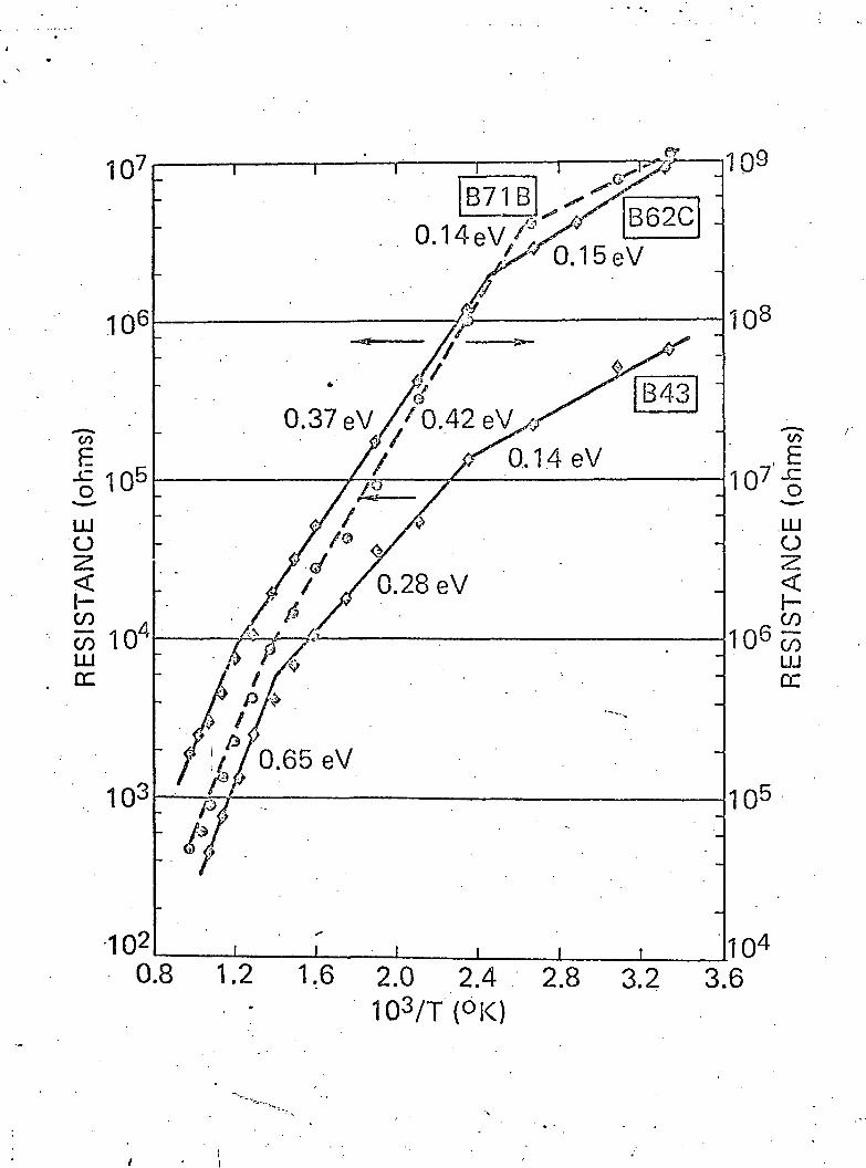
V. Electrical Measurements
Electrical measurements were carried out on the samples
described here in an effort to distinguish differences between
—V—
( 8 )these pure samples and the ones described previously v '.
Resistance versus 1/T measurements were made in a pure argon
atmosphere in a tube furnace with gravity contacts onto titanium
deposited electrodes. The results are given in Fig. 4 for samples
containing carbon, samples from a molybdenum crucible, and a
sample deposited on a hot substrate. In each case, the curves
could be broken into three straight lines representing three
activation energies. Above 700°K, all of the samples appear to
show an intrinsic slope of .65 eV. This would lead to a band gap
(8 }of 1.3 eV, which is exactly that reported previously v . The
activation energy at around 0.3 eV and 0.15 eV was also similar
to those reported previously. There is thus little difference
between the values of activation energies of more pure films and
the films described earlier. These values are also similar to
those found by various authors in crystalline boron . The1 * - •
source of the activation energies is unknown, however it should
be noted that the films may still contain a carbon impurity which_' (A)
-could—account—for~at—least one of the energy levels .
All of the samples exhibit p-type conductivity and have a*5 A
resistivity of 10 - 10 • ohm-cm, measured by both a 2-contact and
a 4-contact technique. ; The value is considerably lower than .
1210 ohm-cm reported previously by us , and even lower than that
reported for crystalline boron *• '. However, this low value of
resistivity is the same as that found in carefully prepared films
by "intrinsic thermometer method" *• . The present films were- ° ' _7
deposited at 1000A/min at less than 10 torr in contrast to theo C
previous films deposited at 200A/min at 2 x 10" torr. Also, as
-8-
discussed in Section III, these improved conditions have led to
more pure films. The enormous decrease in resistivity with increased
purity could then only be accounted for by the presence of large
amounts of compensating impurities in the previous films and .
perhaps even in crystalline boron.
The previous samples deposited at 10~ torr would readily
switch from a low to a high conduction state in the manner previ-
ously described *• '. The low resitivity of the present samples
makes switching difficult since it is hard to impose a high field.
At liquid notrogen temperature, however, some switching does occur.
The effects of joule heating and the analysis of pre-switching
(13)non-linear currents has been described elsewhere . . .
VI. Optical Measurements
The spectrophotometer used to measure transmission coefficient T
.is a double beam instrument in which the monochromatic beam from
a SPEX Model 1400 double grating monochromator is divided by a
-beam- spTitter ~and arrowed" to> pass "throughn. ielitical. optical
elements before being recombined and fo'cused onto the detector.
.One leg of the beam is passed through the sample and the other
through a reference absorber (usually air) before the beams are
recombined. The sample and reference beams are chopped at two
different frequencies (175 Hz and 200 hz) by tuning fork light
choppers. The two frequency components of the detector signal are
separated by two lock-in amplifiers in a manner such that a voltage
proportional to the ratio of the sample signal intensity to the
reference signal intensity is- available for display on a strip
chart recorder. The wavelength resolution of the instrument is a
-9-
function of wavelength and slitwidth. In all cases it is less
-3 -3than 5 x 10 pm and is usually about 10 [im. . The photometric
precision is T±0.005 over most of the range of the instrument.
The photometric accxiracy in the visible region, for which
calibrated standards are available, is also T±0.005.
The optical constants were determined by measuring the
transmission through two samples, deposited at the same time, which!
were identical except for thickness. The procedure for obtaining
the optical constants from the transmission data has already been
described elsewhere . The value of the refractive index n at
X ~ 2.5 ptm was found to be 3.45, which is to be compared with the
value 3.1 for crystalline boron. This increase of approximately
10% is similar to the ones reported for amorphous forms of
silicon *• ' , germanium^ ' and many other covalently bonded
semiconductors which have the same short range order in their
crystalline and amorphous states.
The absorption coefficient a as a function of energy in the
range of 0.6-1.7 eV is shown in Fig. 5 and compared with earlier
results on amorphous boron . For completeness, the data on
(17 18^single crystals of B-rhombohedral boron v 'is also included.
The two sets of samples used in the present work were from 0.13
to 0.43 ^m thick, allowing accurate measurements of transmission
up to 1.7 eV. The absorption values in amorphous boron (Fig. 5)
are higher than in the crystalline boron and the absorption edge
is considerably broadened and shifted towards lower energies. The
-10-
f 14 15situation is again similar to that in amorphous silicon v i*-^*
and germanium '
Compared to our previous data, the absorption coefficient
is somewhat higher in the entire energy region; moreover, the
sharper rise in absorption starting at 1.3 eV (see Fig. 5) is
not discernible in the present data. The analysis of the data
4 -1shows that the values of 0 10 cm , in the energy range 0.9 eV
—1.65 eV, can be fitted very well to the expression
- %)2
with the "band gap" Eg = 0.62 eV. For lower values of a, the
data can be fitted to an exponential e a with the characteristic
energy Ea = 0.12 eV. In terms of the recent models introduced
to discuss the density of electronic states in disordered semi-
conductors, E corresponds to allowed optical transitions betweeno
band-like states, while Ea is an activation energy between states
in the exponentially decaying tails of the density of _st.ajtes_,
induced by disorder. Though such models have been successfully
applied to explain optical absorption in disordered semiconductor
alloys and even in amorphous germanium and. silicon, with admittedly
less success, their usefulness is still a subject of lively
controversy.
Conclusions
In the present paper, techniques for the production of
relatively pure films of amorphous boron have been described. A
quantitative method for determining impurity content and ion-
-11-
clustering effects in the films has been discussed. Elimination
of the graphite crucible and the combination of lower deposition
pressures and higher deposition rates has drastically reduced
the carbon content of the films. The reduction in impurity
content has, however, led to an.enormous drop in the value ofQ
resistivity (by a factor of 10~) as compared to the earlier
2films, and the values are even lower (by a factor of 10 ) than
those reported for crystalline boron. It is therefore postulated
that previous samples and perhaps crystalline boron contain a
large amount of compensating impurities. This point needs
further confirmation by deliberate doping of pure films with com-
pensating impurities and checking the purity of crystalline boron.
Such an analysis would also throw light on the effect of compen-
sating impurities in the switching effect.
It should be noted that the reduced impurity content has
not led to any significant changes in the thermal activation
energies. The values of the activation energies, 0.15 eV, 0.35 eV
and 0.65 eV are almost identical to those reported, previously.
This would indicate that the present films still contain the
impurities responsible for the levels associated with these
activation'energies but the densities of these levels have been
reduced. The highest activation energy for conduction (0.65 eV)
found at temperatures exceeding 700°K would lead to a thermal
gap of 1.3 eV. However, some caution should be exercised in the
interpretation of this value or the smaller one obtained from
optical measurements (0.62 eV) as a "band gap". The relationship
-12- :•
of these values to the concepts borrowed from band theory of
crystalline solids is not entirely clear. Such large differences
between the values of electrical and optical "band gap" are
common when dealing with amorphous semiconductors and further
work, particularly on the annealing of the samples, is planned
to resolve them. .
Acknowledgments
The authors are happy to acknowledge the work of Kenneth
Hoggarth in depositing boron films, and of Frank Satkiewicz
of GCA for carrying out the sputter-ion source mass spectra
analysis.-
REFERENCES
(1) K. Moorjani, C. Feldman,, Proc. of International Symposiumon Boron, Warsaw, 1968, Electron..Technology (Warsaw)3, 265 (1970).
(2) C. Feldman, F. Satkiewicz, Thin Solid Films, 12, 217 (1972).
(3) K. Katada, Japanese J. App. Phys., 5, 582 (1966).
(4) O. A . Golikova, E. N. Nikitin, F. N. Tkalenko, SovietPhysics - Semiconductors, 4, 1193 (1971).
(5) P. E. McElligott, R. W. Roberts, J. Chem. Phys. 46,273 (1967).
(6) M. G . Ingram, R. C. Porter, W. A. Chupha, J. Chem. Phys.,25, 498 (1956).
R. P. Burns, A. J. Jason,'M. G. Ingram, J. Chem. Phys.,46, 394 (1967).
(7) .A. R. Badzian, Refr. 1, page 143.
(8) C. Feldman, F. Ordway, W. Zimmerman III, K. Moorjani.Boron 2, Ed. Gaule, Plenum Press, New York (1967).
(9) M. Prudenziati, G. Majini, A. A. Quaianta, J. Phys. Chem.Solids, 33, 245 (1972).
Sh. Z. Dzhamagidze, Yu. A. Mal'tsev, Soviet Physics -Semiconductors, 3, 80 (1969).
(10) D. Geist, J. Meyer and H. Peussner, Refr. 1, page 207.
G. V. Tsagareishvili, F. N. Tavadze, G. Sh. Darsavelidzeand V. Sh. Metreveli, Refr. 1, p. 281.
E. I. Adirovich and L. M. Gol'dshtein, Soviet Phys. -Solid State 8, 1968 (1967). • •
(11) E. I. Adirovich and L. M. Gol'dshtein, Soviet Physics -Semiconductors, 3, 196 (1969).
(12) C. Feldman, W. A. Gutierrez, J. Appl. Phys., 39, 2747 (1968)
C. Feldman, K. Moorjani, J. Non-Crystalline Solids, 2,82 (1970).
(13) K. Moorjani, C. Feldman, J. Non-Crystalline. Solids, 4,248 (1970).
REFERENCES (page 2) - ..*%.
(14) N. A. Blum, C. Feldman, K. Moorjani, Bull. Am. Phys.Soc., 17, 114 (1972)
(15) M. II. Brodsky, R. S. Title, K. Weiser, and G. D. Petit,Phys. Rev., Bl, 2632 (1970).
(16) M. L. Theye, Optics Comm. 2, 329 (1970).
(17) E. Kierzek-Pecold, J. Kolodziejczak and I. Pracka, PhysStat. Sol. 22, K147 (1967).
(18) H. Werheit, A . Hausen and H. Binnenbruck, Phys. Stat.Sol. 42, 733 (1970).
(19) R. Grigorovici and A. Vancu,- Thin Solid Films 2, 105(1968).
(20) K. L. Chopra and S. K. Bahl, Phys. Rev. Bl, 2545 (1970)
I :
CO"Z.OHQZOo•2.O
coOQ.LUQ•z.O
.CCoCO
COLU
<CC
CQIDCO
cc—3
UJ ^H — "«^< CC c<
_ DCS LU >
LU Q -*03 CL
Q.
3 s yCO jff
+_, £f-
HCO LU 2O S -m H !§•
Q
2^ o oID — —(_) OL UJ
" 2 D.*•* ^ UJ
Q
LU
CQ
O
CC .O
CD
LU_JQ.
^CO
(O1 —
XLUCC
Q_
0OCO
CO"'
OCDCN
CNr~
OCN
ca1Or—
X
CN
O
.^^1en
rah~
COCO
OO
q
0
CN
inc>
inCN1 —
co
o*"~XinCO
en
O
oCO
1CQ
CM
OC/3
COCO
0OCN
OCN
O0CN
COCOo
CO
CO
1o*
X
CN|~sT
o
CNCO
1en
(O1 —
COCO
0oCO
CN"'
ooCO
COino
in
1oT~XT-
^
O
0COCD
1CO
CN
gCO
COCO
inCO
V-"'
ooO)
COCNO
CO
1o1 —X
CO
0s
enr-
1en
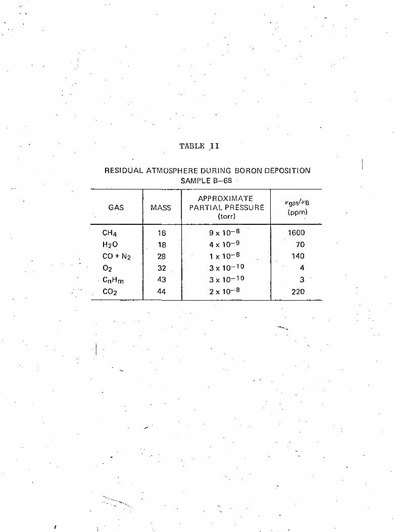
TABLE II
RESIDUAL ATP/!OSPHERE DURING BORON DEPOSITIONSAMPLE B-68
GAS
CH4
H2O
CO + N2
02
CnHm
C02
MASS
16
18
28
32
43
44
APPROXIMATEPARTIAL PRESSURE
(torr)
9x10⁻⁸
4x10⁻⁹
1x10⁻⁸
3x10⁻¹⁰
3x10⁻¹⁰
2x10⁻⁸
"gas/"B(ppm)
1600
70
140
4
3
220
x-vfl) X~N
0 >•H Q)
r-l COt~ o
1 C OCQ Or-l
^x v, ••
CJ >CO H <Dto
1 C3 0CQ O O
Ctt >O <U
CM -HtD CO Oi m
CQ C CM
^
CJ >O EH 0toI C O
CQ o m
'e? >\H E~i Q)^J*
1 C Oen o m
^xpq
Q)
J O^> OCQ r-H
Q)^^^
JM 0N-x O
1o•Jw >M Q)
0mCM
COwMCJw&
O O O C M O O O i - l t DO O O r H O O O O i HO CO O CO ^f
•» £ •* «v
m in r-<2 CO
I*-.
O O O C M O O O O ^O O O r - I C M M < t O C MCO r-i O iH
i ^ to"
toO O O C O . Q O O O r HO CJ) O ?5 i O x-x
CJ) O CM P55
N O r - l
A
mo o o c o m o i n o i - cO C O O C M r - I C O C J ) - ^to i-i o p
•* •* ' 55
in rH• ^^
O O O O Q O O O O C MO C J ) O r - l j 5 r - < O C O0 0 r-<v00 CJ)00
V. ^ • ^ • ^ • P P o o o t >^ ^ ^ 55 55 CO 0CQ CQ CQ r-i . . .
~<J) O) CO O)• « • •
C M i n r n i n t o c s j c o t o or-l CM 0r-l iH
CO CO
C M t ^ J O O C M C O O i n^ 0 CM CM 0 CO
CM CM
• r-l
- •' x-> 'x^» ""OW CQCQ . ^• > - ' * * r t b f l r - l 'H dO < 5 O 5 5 ^ < C O ^ C J
.- .
P P 0 055 55 CO O
CO
P O 0 O55 m CM rj<
rH
P P 0 055 55 CO M<
TJ< o in oCO CO
V
-.
r-i m p oCM rH 55 CO
I rH - •V
. fc
p p p p»y- £2 JZ ^"
h- O>, *
t> CO O r-l OCO H rH
t O)
f^ CO O iH OCO H r-l
•H to 0)H > O Cn CQ
•d oo uo S0) M
p ^<D
•P -P
55 «
D n
•OO-p'O
nJ14
W
CQ
f-*O
w'ocS
CQ
Figure Captions
Fig. 1 Arrangement in bell jar showing source crucible
with molybdenum .liner and electron gun.
Fig. 2 Polyatomic mass spectrum of a boron film
(Sample 68-C).
i
Fig. 3 Relative distribution of B^ ion clusters from
bulk and three different films of boron.
Fig. 4 Resistance as a function of reciprocal temperature
for three different films of boron.
Fig. 5 Optical absorption coefficient as a function of
energy.
• »-•' present data on amorphous boron
previous data on amorphous boron(Refr. 1)
data on crystalline boron(Refr. 17)
data on crystalline boron(Refr. 18)
c
10-7
10-8
Q.ECO
c/510-9
10-10
io-i2L_ j_J
, (BH+)
B2+
CH+
0+
B2H+, Na
Si+CO+
COH+K+
B4-
B6+
10
cCD
ifOJ
ccLUh-co
O
OocOCO
^1
1-2
10-3
io-4
I r
*. B44
B68C
I I I I I I
B3+ B4
+
m/e
107
106
CO
E
LUO
V)
wLJUCC
105
0.376V//0.42 eV
10
103
102
0.28 eV
' ! / /0.65eV
/»/6 A
0.8 1.2
109
108
LLJO
UJDC
105
104
2.0 2.4 2.8 3.2 3.6103/T
0.5 0.7 0.9 ,1.1 1.3 1.5ENERGY(eV)
1.7 1.9
JOURNAL OF NON-CRYSTALLINE SOLIDS 11 (1972) 242-246 © North-Holland Publishing Co.
LETTERS TO THE EDITOR
THE CRYSTALLIZATION OF AMORPHOUS
SILICON FILMS*
NORMAN A. BLUM and CHARLES FELDMAN
Applied Physics Laboratory, The Johns Hopkins University, 8621 Georgia Avenue, SilverSpring, Maryland 20910, U.S.A.
Received 31 May 1972
It is well known that the heating of vacuum deposited amorphous siliconfilms above about 700°C produces an irreversible transformation to thecrystalline state1'2). Films deposited on substrates near or below roomtemperature may, furthermore, tend to contain voids3). At higher substratetemperatures the relative volume of voids diminishes, but the films maybegin to crystallize. The lowest practical crystallization temperatures andtimes should be used to avoid introduction of impurities. It is therefore im-portant to know in some detail how deposition temperature and subsequentannealing influence the approach to crystallinity in amorphous silicon films.The crystallization process has been followed by observing optical trans-mission changes in the films as they are heated at various temperatures. Itwill be shown that the crystallization process is a gradual one which takesplace at any finite temperature. Heat treatment which is likely to annealaway the voids is also likely to make the sample tend toward crystallinity.
The samples were prepared by electron beam vacuum deposition ontopure fused silica substrates at about 2 x 10~7 torr at rates from 200 to 300 A//min with the substrate temperature rising from 200°C to 300°C during thedeposition. Pre-deposition pressure was about 5x 10~9 torr. The source tosubstrate distance was about 15 cm. For the experiments described here, thefilm thicknesses were approximately 5000 A. Film thicknesses were measuredby a multiple beam interference technique and revealed a decrease in thick-ness, and thus also in the volume, in going from amorphous to crystallizedsamples, of about 8.2%. Samples were heated in a tube furnace flowing withpure argon for a fixed time and temperature and then removed from thefurnace and examined optically.
* Work supported by NASA under Grant No. NCR 21-009-033 and by Naval OrdnanceSystems Command, Contract N00017-72-C-4401, Task A13B.
242
CRYSTALLIZATION OF AMORPHOUS Si FILMS 243
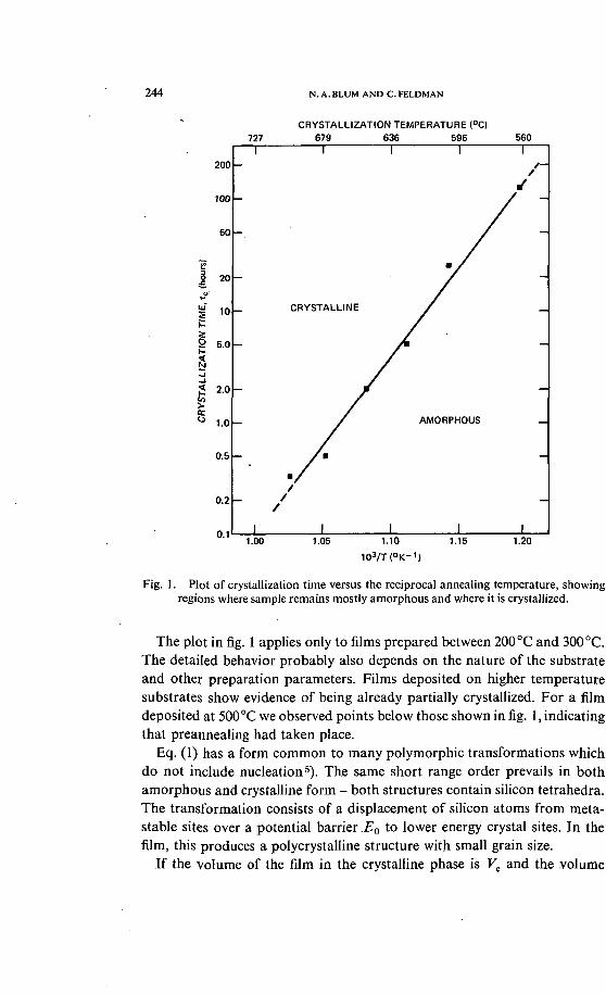
For incident photon energies above about-2.0eV both amorphous andcrystallized Si films are heavily absorbing. At 2.6 eV, for example, crystallinefilms exhibit an absorption coefficient a of about 2x 104cm~1, while "asdeposited" (amorphous) films show an a at least three orders of magnitudegreater. Thus, the transmission of the films at 2.6 eV (4800 A) is a sensitiveindication of the degree of crystallinity or amorphicity. An arbitraty criterionfor "onset of crystallinity" used here is that 5000 A thick samples have atotal external transmittance of 5% (corresponds approximately to a = 6 x 10⁴)at a wavelength of 4800 A. Samples meeting this criterion are nearly crystal-lized; further heating results in only a slight increase in transmission. Theresults are independent of the exact details of the criterion as long as itgives an indication of a phase state somewhere between the two extremes; acriterion based upon maximum rate of change of the observed parameterwith annealing is clearly most useful. In practice, since the sample trans-mission was not monitored during the annealing process, the. times areapproximate. The operational procedure was to estimate the time to reachthe criterion and anneal for that length of time at constant temperature. Ifthe criterion was not met (i.e., the transmission at 4800 A was appreciablydifferent from 5% at 4800 A), then the anneal was repeated with anothersample at the same temperature for a shorter or longer time depending onwhether the sample was on the amorphous or crystalline side of meeting thecriterion. The procedure was repeated until a satisfactory result was obtained.
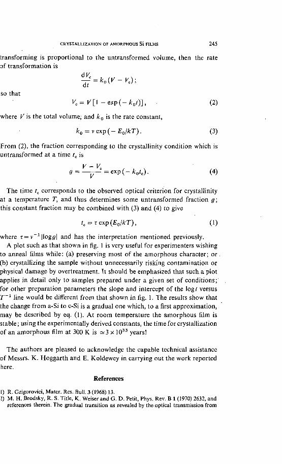
Using the above criterion, the time to reach "onset of crystallinity" ?c wasdetermined as a function of annealing temperature T for a sample whichwas divided into pieces, each annealed and analyzed separately. This assuredthat all samples started out identical to one another. The plot of log ?c versusT'1, shown in fig. 1, gives a straight line, indicating that the simple rateexpression
(1)
is a reasonable approximation relating tc and T. Above and to the left of theline is the area of certain crystallinity, below and to the right lies the area ofamorphicity. Close to the line is the intermediate region where the sample isin transition between the two states.
In eq. (1), T is associated with the characteristic time of a microscopicinteraction between neighboring atoms, while E0 is identified with the activa-tion energy between the metastable amorphous state and the stable crystal-line state. From fig. 1, r^5x 10~14sec and £0^3.1 eV, both figures arereasonably consistent with the identification of i as an interaction timebetween atomic neighbors, and E0 as an activation energy for self diffusionin Si 4).
244
727
200
100
50
N.A.BLUM AND C.FELDMAN
CRYSTALLIZATION TEMPERATURE (°C)679 636 596 560
20
10
5.0
CRYSTALLINE
1.0 AMORPHOUS
0.5
0.2
0.11.00 1.05 1.10 1.15 1.20
Fig. 1. Plot of crystallization time versus the reciprocal annealing temperature, showingregions where sample remains mostly amorphous and where it is crystallized.
The plot in fig. 1 applies only to films prepared between 200 °C and 300 °C.The detailed behavior probably also depends on the nature of the substrateand other preparation parameters. Films deposited on higher temperaturesubstrates show evidence of being already partially crystallized. For a filmdeposited at 500 °C we observed points below those shown in fig. 1, indicatingthat preannealing had taken place.
Eq. (1) has a form common to many polymorphic transformations whichdo not include nucleation5). The same short range order prevails in bothamorphous and crystalline form - both structures contain silicon tetrahedra.The transformation consists of a displacement of silicon atoms from meta-stable sites over a potential barrier .E0 to lower energy crystal sites. In thefilm, this produces a polycrystalline structure with small grain size.
If the volume of the film in the crystalline phase is Ve and the .volume
CRYSTALLIZATION OF AMORPHOUS Si FILMS 245
transforming is proportional to the untransformed volume, then the rateof transformation is
so that
X c =X[ l -exp( -*oO] , (2)
where V is the total volume, and k0 is the rate constant,
(3)
From (2), the fraction corresponding to the crystallinity condition which isuntransformed at a time tc is
k0tc). (4)
The time ?c corresponds to the observed optical criterion for crystallinityat a temperature T, and thus determines some untransformed fraction g;this constant fraction may be combined with (3) and (4) to give
fc = Texp(£0/£T), (1)
where T=v~ 1 | log# | and has the interpretation mentioned previously.A plot such as that shown in fig. 1 is very useful for experimenters wishing
to anneal films while: (a) preserving most of the amorphous character; or .(b) crystallizing the sample without unnecessarily risking contamination orphysical damage by overtreatment. It should be emphasized that such a plotapplies in detail only to samples prepared under a given set of conditions;for other preparation parameters the slope and intercept of the log; versusT'1 line would be different from that shown in fig. 1. The results show thatthe change from a-Si to c-Si is a gradual one which, to a first approximation,may be described by eq. (1). At room temperature the amorphous film isstable; using the experimentally derived constants, the time for crystallizationof an amorphous film at 300 K is ~3 x 1033 years!
The authors are pleased to acknowledge the capable technical assistanceof Messrs. K. Hoggarth and E. Koldewey in carrying out the work reportedhere.
References
1) R. Grigorovici, Mater. Res. Bull. 3 (1968) 13.2) M. H. Brodsky, R. S. Title, K. Weiser and G. D. Petit, Phys. Rev. B 1 (1970) 2632, and
references therein. The gradual transition as revealed by the optical transmission from
246 N. A. BLUM AND C. FELDMAN
a-Si to c-Si as a function of annealing temperature can be seen from fig. 4 of thisreference. For their preparation parameters and crystallization criteria, Brodsky et alreport that the film crystallized during the 500°C annealing cycle.
3) T. M. Donovan and K. Heinemann, Phys. Rev. Letters 27 (1971) 1794;F. L. Galeener, Phys. Rev. Letters 27 (1971) 1716.
4) A. Seeger and M. L. Swanson, in: Lattice Defects in Semiconductors, Ed. R. R. Hasi-guti(Univ. of Tokyo Press, 1968) p. 125.
5) J.W.Christian, The.Theory of Transformations in Metals and Alloys (Pergamon,Oxford, 1965) pp. 16-22.
Reprinted from the Proceedings of the
Second International Conference on
CONDUCTION IN LOW-MOBILITY MATERIALS
CAJ N3
EILAT, ISRAEL
5-8 April 1971
TAYLOR & FRANCIS LTDInternational Scientific Publishers
10-14 Macklin Street, London WC2B 5NF
Pair Approximation in the Coherent Potential Theoryof Disordered Solids
By K. MooBJANifApplied Physics Laboratory, The Johns Hopkins University,
8621 Georgia Avenue, Silver Spring, Maryland 20910
and T. TANAKA$Catholic University of America, Washington, B.C. 20017
and S. M. BOSE|Drexel University, Philadelphia, Pennsylvania, 19026§, andCatholic University of America, Washington, D.C. 200017
ABSTRACTThe paper develops a self-consistent method for studying disordered
systems with diagonal as well as off-diagonal disorder. The method hasgeneral applicability to any disordered system and in the present analysisis applied to a monoatomic system where disorder arises due to a randomdistribution of vacancies.
§ 1. INTEODUCTIONTHE equilibrium and the non-equilibrium aspects of disordered solidshave attracted a great deal of attention recently, experimentally as well astheoretically. (See various papers in the proceedings edited by Mott1970.) In particular, many different theoretical approaches are availablefor discussing the properties of disordered binary alloys. The principalamong these is the recently introduced coherent-potential approximation(CPA) by Soven (1967).
The application of the CPA to a disordered binary alloy is based onreplacing the atomic potential at each lattice site by an undeterminedcoherent potential. The multiple scattering effects from the actualpotentials are described via a T-matrix, where the scattering potential isthe difference between the actual potential and the coherent potential.In an exact formulation the coherent potential can be determined self-consistently from the condition that the configurational average of theT-matrix must vanish. In the CPA this condition is replaced by a weakerone requiring the configurational average of fhe atomic T-matrix to vanish.
f Partially supported by Naval Ordnance Systems Command, Contract No.NOw-62-0604-c, Task A13B, and NASA Grant No. NGR-21-009-033.
J Supported by National Aeronautics and Space Administration Researchunder Grant No. NASA NGR-09-005^072.
§ Present address 1
168 Conduction in Low-mobility Materials
The success of the CPA is evidenced by a number of recent papers whichhave used the CPA to discuss the static and the dynamic aspects ofdisordered alloys (Velicky, Kirkpatrick and Ehrenreich 1968, Velicky1969, Velicky and Levin 1970, Kirkpatrick, Velicky and Ehrenreich 1970,Economou, Kirkpatrick, Cohen and Eggarter 1970, Stroud and Ehrenreich1970, Soven 1970). The method, however, is applicable to alloys possess-ing diagonal disorder only, thus making it useful mainly for alloys com-posed of isoelectronic atoms. Recently, attempts have been made toinclude off-diagonal randomness in approximations similar to the CPA(Berk 1970, Foo, Amar and Ausloos 1970).
In the present analysis a more general self-consistent approach isdeveloped which is capable of dealing with solids exhibiting diagonal aswell as off-diagonal disorder. The general ideas followed are similar innature to those in the CPA. The off-diagonal randomness arises due to therandomness in the hopping energy of an electron between nearest-neigh-bour atoms. This necessitates the introduction of a wave-vector depen-dent coherent potential in contrast to the wave-vector independent co-herent potential of the single-site CPA.
The model and the formalism are described in the next section and theresults are discussed in the last section.
§ 2. FORMALISM
The present formalism concerns itself with the effect of diagonal andoff-diagonal disorder on the electronic density of states of a one-bandsystem. The method has general applicability but we focus our attentionon a monoatomic system. The disorder in such a one-component systemcan be simulated by removing a certain fraction of atoms at random, froman ordered lattice. The probability of occupation of a given lattice siteis then given by c(0 < c < 1), where c = 1 represents the completely orderedlattice.
We write the total Hamiltonian for the above system as a sum ofHamiltonians describing the pairwise interaction of a given particle withits nearest neighbours.
......... (1)
where the summation is over all nearest-neighbour pairs a and
+Wlm(al*am + am*al). . (2)
Here Wu = ^l and W lm= TF/x,/xm= Wml. The disorder is incorporatedthrough the variable /x, which is unity for an occupied site and zero other-wise. In the above definitions, e denotes the potential energy at eachlattice site while W is the hopping energy between two nearest neighbours.Finally z is the number of nearest neighbours.
Conduction in Low-mobility Materials 169
The equilibrium quantity of interesst is the electronic density of statesp(E), given by the well-known expression
p(E)---Im Trace 0(E) ...... (3)TT
where the functional dependence of the Green's function on the complexenergy E is given by
and the bar denotes the average over all possible configurations of thesystem.
To discuss the effects of multiple scattering of an electron from systemsrepresented by the Hamiltonian (1), we introduce an effective mediumdescribed by the Hamiltonian,
where S0( = S,,) and S1( = SIm) are respectively the diagonal and the off-diagonal coherent potentials, as yet undetermined. It is desirable that20 and S1 be determined self-consistently.
The multiple-scattering effects are now easily described by the T-matrix,
...... (6)
where the configurationally averaged Green's function is given by
S<*)--^. . . . . . . . . ( 7 )
From the relationship
G = G + GTG, ...... . . (8)
we note that the configurational average of the T-matrix must, vanish.That is,
T = 0 ......... (9)
The eqn. (9) represents the self-consistent condition which determinesthe coherent potentials S0 and Ex ; which in turn determine the densityof states via eqns. (7) and (3).
In the above analysis the problem has been treated exactly, but toproceed any further some approximations are needed. In the CPA, thecondition represented by eqn. (9) was replaced by a simpler one requiringthe configurational average of the atomic ^-matrix to vanish. Such asingle-site approximation was adequate to determine the single, k-independent, coherent potential introduced there. Below we discuss thetwo-sites approximation appropriate to the system represented by theHamiltonian (1).
170 Conduction in Low-mobility Materials
The full T-matrix (eqn. (6)) can be written in terms of two-sites^-matrices by the conventional expression,
where the two-sites (-matrix is given by
(ii)
In eqn. (10), the restricted summations imply that the successive pairindices cannot be equal ; that is, in the third term a /J and /J y buta = y is allowed.
The self-consistent condition (9) is now replaced by a weaker one,
*a = 0 ......... (12)
This matrix equation leads to two equations, one for the diagonal matrixelements (tmm = Q) and the other for the off-diagonal matrix elements(t(m = 0) and they determine the two unknowns S0 and £v
In Wannier representation, the matrix elements of the ^-matrix arewritten as
'to = ( Wlm - Sj) + ( W „ - S0) [g0tlm + 9ltmm]+ (Wlm-X1)[gltlm + g0tmm] (13)
and
\, (14)
where I and ra are nearest neighbours. The quantities g0( = Gmm) andffi( = @im) are obtained from the matrix elements of the Green's function,
- 1 _ exp [ilc . (I — m)l
In eqn. (15), the structure factor -y(k) = exp (ik . A), where A is thenearest-neighbour vector. A
Equations (13) and (14) can now be solved for tmm and tlm and therequirement that their configurational averages vanish, leads to theequations
(16)
Conduction in Low-mobility Materials 171
and
'• (17)
where
-l, (18 a)
-l (186)
andA. = (0oa-fc'HSi8-So8]-ZSrfi-22000-1. . . (18 c)
The formulation is now complete since eqns. (16) and (17) can, inprinciple, be solved for the two unknowns S0 and 2^ in terms of e, W andthe energy E. The density of states in terms of S0 and 2j is easilyobtained by rewriting eqn. (3) as
P(E)=--ImGm m(E)=:--Img0 , . . . . (19)77- 77
or
Pa t .W=-^Im<70 , (20)
where pat_(E) is the density of states/atom and g0 is obtained from eqn. (15).The numerical solution of eqns. (16) and (17) for a three-dimensional
solid is not entirely simple. The corresponding calculations arenowunder-way and will be reported in the near future. However, the simpler prob-lem of one-dimensional disorder chain lends itself to an exact analyticsolution in the present formulation and is discussed in the next section.
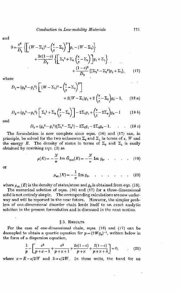
§ 3. RESULTSFor the case of one-dimensional chain, eqns. (16) and (17) can be
decoupled to obtain a quartic equation for p = (2Wg0)~l, written below inthe form of a dispersion equation,
1 f c2 c2 2c(l-c) 2(1 -c)H-- T + T+— +— U = °. •p \_p+x— 1 p+x+ l p+x p + x + SJ
where x=E — e/2W and 8 = e/2l7. In these units, the band for an
172 Conduction, in Low-mobility- Materials
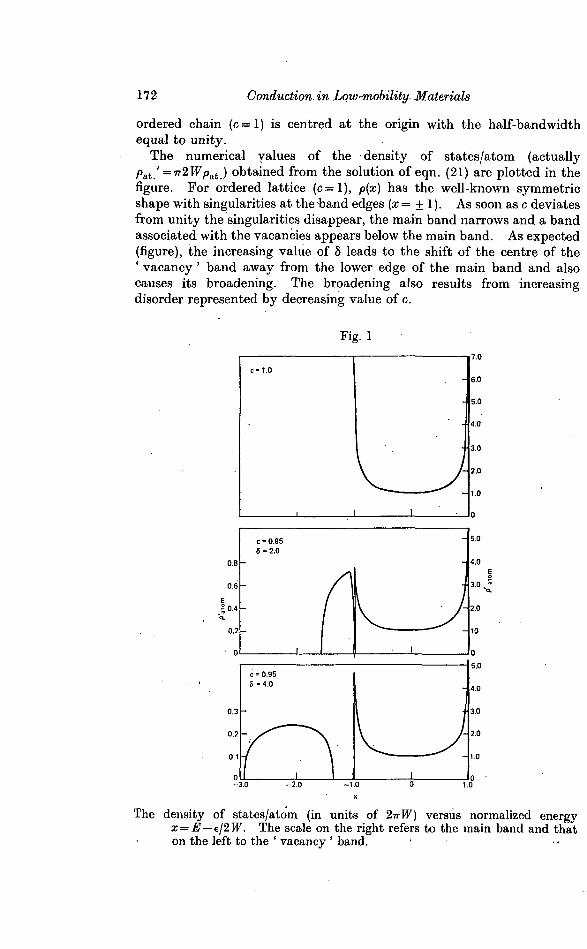
ordered chain (c=l) is centred at the origin with the half-bandwidthequal to unity.
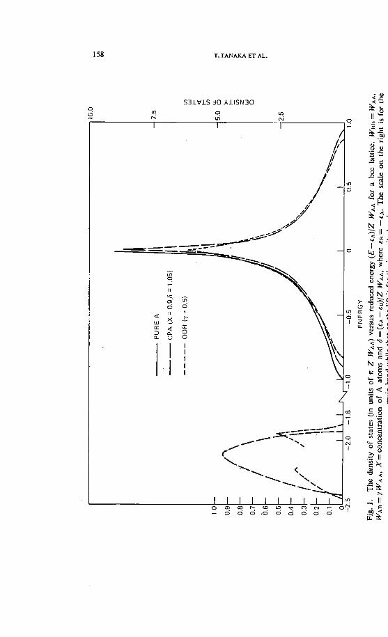
The numerical values of the density of states/atom (actuallypat ' = 7r2 Wp&k) obtained from the solution of eqn. (21) are plotted in thefigure. For ordered lattice (c=l), p(x) has the well-known symmetricshape with singularities at the band edges (x = ± 1). As soon as c deviatesfrom unity the singularities disappear, the main band narrows and a bandassociated with the vacancies appears below the main band. As expected(figure), the increasing value of 8 leads to the shift of the centre of the' vacancy ' band away from the lower edge of the main band and alsocauses its broadening. The broadening also results from increasingdisorder represented by decreasing value of c.
Fig. 1
The density of states/atom (in units of 2-TrW) versus normalized energyx = E — f/2W. The scale on the right refers to the main band and thaton the left to the ' vacancy ' band. •
Conduction in Low-mobility Materials 173
The important question of whether these states, for a three-dimensionaldisordered solid, are localized in nature, can only be answered by calculat-ing conductivity. Such a calculation, in the formulation presented here,is now under way.
ACKNOWLEDGMENTS
K. Moorjani would like to express his sincere thanks to S. Favin of theApplied Physics Laboratory for his help with the computer programming.
REFERENCESBEBK, N. F., 1970, Phys. Eev. B, 1, 1336.EcoNOMOtr, E. N., KIBKPATBICK, S., COHEN, M. H., and EGOARTEB, T. P.,
1970, Phys. Rev. Lett., 25, 520.Foo, E-Ni., AMAB, H., and AUSLOOS, M., 1970, Bull. Am. phys. Soc., 15, 774.KIBKPATBICK, S., VELICKY, B., and EHBENBEICH, H., 1970, Phys. Rev. B, 1,
3250.MOTT, N. F,, 1970, Proc. Int. Conf. on Amorphous and Liquid Semiconductors,
Cambridge, England.SOVEN, P., 1967, Phys. Rev., 156, 809 ; 1970, Ibid., B 2, 4715.STBOTTD, D., and EHBENBEICH, H., 1970, Phys. Rev. B, 2, 3197.VELICKY, B,, 1969, Phys. Rev., 184, 614.VELICKY, B., KIBKPATBICK, S., and EHBENBEICH, H., 1968, Phys. Rev., 175,
747.VELICKY, B,, and LEVIN, K., 1970, Phys. Rev. B, 2, 938.
3URNAL OF NON-CRYSTALLINE SOLIDS 8-10 (1972) 155-159 © North-Holland Publishing Co.
COHERENT POTENTIAL THEORY OF
OFF-DIAGONAL RANDOMMESS : BINARY ALLOY
T. TANAKA and M. M. SOKOLOSKI*t
Department of Physics, The Catholic University of America,Washington, D.C. 20017, U.S.A.
K. MOORJANI**
Applied Physics Laboratory, The Johns Hopkins University,Silver Spring, Maryland 20910, U.S.A.
and
S. M. BOSE*
Department of Physics, Drexel University, Philadelphia,Pennsylvania 19026, U.S.A.
rhe single-site coherent potential approximation (SS-CPA) for a disordered binary alloys extended in a self-consistent manner to the case of off-diagonal randomness. The densityrf states for a bcc lattice is calculated in the split band limit for no correlation betweeniiagonal and off-diagonal randomness and compared with the ordered and SS-CPA densityDf states.
1. Introduction
Ever since Soven1) introduced the single-site coherent potential approxi-mation (SS-CPA) for the study of disordered systems, many papers2) haveapplied the approximation to the calculation of the properties of disorderedsolids. The SS-CPA is applicable only to the case of diagonal randomness,and these results have been criticized by Stern3).
Previous attempts have been made to extend the CPA to off-diagonalrandomness4). A self-consistent extension is discussed here.
2. Theory
The disordered binary alloy A^Bj_^ is characterized by the Hamiltonian
r,*J/> W ( m<m|, (I)
* Supported in part by NASA grant # NGR-09-005-072.** Supported in part by Naval Ordnance Systems Command, Contract #NOw-62-0604-c,Task A13B, and NASA grant #NGR-2 1-009-03 3.t Present address: Harry Diamond Laboratories, Washington, D.C. 20438, U.S.A.
155
156 T.TANAKA ET AL.
where the atomic energy, e,, can take the value eA or eB and the off-diagonalmatrix element, Wlm, can assume the values WAA, WAB, or WBB.
In the spirit of the SS-CPA, a configuration-independent Hamiltonian isintroduced by
(2)
where Z0 = ZU and Il=Ilm are the diagonal and off-diagonal coherentpotentials, respectively. The index m in each of the Hamiltonians will berestricted to the first nearest neighbor of /. The Green's functions satisfy theequations (E-H) G=\ and(£-F0) G 0=l and are related by G = G0+G0 xx TG0, where T = H- H0 and the scattering T-matrix is given by T= F + rG0T.
The self-consistency criterion, <C7> = G0 yields <r>=0, where the angularbrackets indicate a configurational average.
Since the operator F consists of diagonal and off-diagonal components,it is convenient to introduce two T-matrix equations corresponding to thescattering from the two components, i.e.,
T^^ + r.GoT,, i = l,2, (3)where
rt = z,r (/) = £, I />(e (-WI, (4)and
) = z l * m \ i y ( w l m - z 1 ) < m \ . (5)The total T-matrix can then be written as
T = Tl + T2 + (T&BV + T2G0AU + AU + BV), (6)where
A = 7\G0T2 , (7)
B = T2G0T, , (8)
U=(1-G 0 A)- 1 , (9)
V=(l -G 0 B) ' 1 . (10)
The first two terms in eq. (6) represent independent scattering from /\ and F2.while the last terms enclosed by parenthesis represent the correlated scatter-ing of Fl and T2.
The two operators, F1 and F2, are written as sums over single entities, i.e.,over single site and pair operators as in eqs. (4) and (5). Then
/,) G0r( /2) + - (ii)This can be written in terms of the single-site Mnatrix
as(/,) G0 t (/2) +- .. (12)
COHERENT POTENTIAL THEORY 157
Since there are two coherent potentials, only two matrix elements of T areneeded, viz., Tu and Tlm, I and m being first nearest neighbor pairs. Simul-taneously, intermediate states appearing in these matrix elements are restrict-ed to first nearest neighbor pairs. A set of terms consistent with this pairapproximation must be extracted from the /-/ and l-m matrix elements ofeq. (12). Hence, scatterings from / and its nearest neighbor site must be con-sidered. The diagonal elements of <Ti> in the pair approximation are
<(W = <*,> + ZtfgltJ(l - 0fom)>, (13)
where t, = (l\t(l)\l), gl = (l\G0\m) and Z = number of first nearest neighbors.Eq. (13) represents the SS-CPA /-matrix vertex corrected for scattering fromits first nearest neighbor.
It can be shown that the off-diagonal matrix elements of < 7\> are
' _ <(rota> = z <0o'«U(i - 0? '/'„)> • (14)If scattering off the nearest neighbor atom is neglected, i.e., #1 = 0, then<(T1),(> = <?,> and <(T1)!m> = 0 which is the SS-CPA result.
Now, if <x= (/, m) designates an (/, m) pair, then
T2 = I. F (a) + I,tf T(a) Go T(>) +.-, (15)
which can be written in terms of a pair-site Mnatrix, t (a) = F (a) + F (a) G0 xx/(a), as
T2=S.t (a) + I^f t (a) GO t (J3) + •• • . (16)
Then in the pair approximation
, (17)and
<(r2),m>=z<o, (18)
where tu = (l\tx\l} and tlm = (l\tx\m). The matrix elements, tn and t lm, arefound by taking the diagonal and off-diagonal matrix elements of the pair-site /-matrix and solving the resultant set of coupled equations. Then
- r2ml9o), (19)
and(20)
Given the matrix elements of Ti and T2 are known, the diagonal andoff-diagonal contributions to the correlation terms in eq. (6) can be found.The self-consistency condition, <T!(> = <T;m>=0, results in two non-linearequations for two unknowns, £o and S^
158 T.TANAKAET AL.
S31V1S dO AJLISN30
COHERENT POTENTIAL THEORY 159
3. Results
These two equations without correlation were solved iteratively for a bcclattice. The density of states is shown in fig. 1 and compared with the SS-CPA. The incompleted part of the curve in the impurity band results fromthe lack of convergence in the solutions. The novel feature is the appearanceof structure in the impurity band which is absent in the SS-CPA. Furtherdetails and discussions will be published elsewhere.
References
1) P. Soven, Phys. Rev. 156 (1967) 809.2) See refs. 3-13', quoted in ref. 3.3) E. A. Stern, Phys. Rev. Letters 26 (1971) 1630.4) K. Moorjani, T. Tanaka and S. M. Bose, Advan. Phys., to be published;.
J. A. Blackman, N. F. Berk and D. M. Esterling, to be published;E-N. Foo and M. Ausloos, J. Non-Crystalline Solids 8-10 (1972) 134.
-1-
Coherent Potential [Theory of a Random Binary Alloy;Effects of Scattering from Two-Sites Clusters
and Off-Diagonal Randomness
KISHIN MOORJANI*Applied Physics Laboratory, The Johns Hopkins University,
Silver Spring, Maryland 20910
and
TOMOYASU TANAKA1"Department of Physics, The Catholic University of America
Washington, D. C. 20017
and
MARTIN M. SOKOLOSKIf
Harry Diamond Laboratories, Washington, D. C. 20438
and
SHYAMALENDU M. BOSE1"Department of Physics, Drexel UniversityPhiladelphia, Pennsylvania 19104
Supported in part by Naval Ordnance Systems Command, ContractN00017-72-C-4401, Task A13B, and NASA Grant NGR-21-009-033.
Supported in part by NASA Grant NGR-09-005-072.
-2-
A one-band model of a random binary alloy A B,X JL "~X
is analyzed in terms of a two-sites coherent potential approx-
imation. In the tight-binding Hamiltonian,. the off-diagonal
randomness is introduced via the composition dependent
hopping energies between nearest neighbor sites. The in-
clusion of the off-diagonal randomness correlates the
scattering from a given site to that from its nearest
neighbors. Such a correlation is incorporated in the
handling of diagonal randomness (arising from the composi-
tion dependence of the atomic potentials) by treating the
diagonal randomness in the pair approximation. The theory
leads to the wave-vector-dependent coherent potentials and•
previous approximations used in this problem are easily
obtained in appropriate limits. The numerical results for
the electron density of states are presented for a number
of different alloys and compared with earlier calculations.
For the case of diagonal randomness only, the present
theory results in the appearance of structure in the
density of states of the minority component band. This is
in contrast, to the results obtained from the single-site
coherent potential approximation, but in agreement with
the recent work of Schwartz and Siggia. The presence of
the off-diagonal randomness leads to further structure in
the density of states.
—3—
I. INTRODUCTION
The coherent potential approach, based on the
multiple scattering formalism of Lax (1951), has proved
to be a useful method for the investigation of disordered
alloys. A simple and elegant version of this approach,
referred to as the single-site coherent potential approxima-
tion (SS-CPA) (Soven 1967, Velicky et al. 1968) has been
fruitfully applied to a random binary alloy A B in whichX JL —X
disorder arises only due to the difference between the atomic
potentials of the two components of the alloy. The hopping
integrals in the tight-binding Hamiltonian are assumed
to be independent of the composition of the alloy and hence
are translationally invariant. Thus, only the diagonal
part of the Hamiltonian is assumed to be random.
The SS-CPA has been elucidated (Velicky et al. 1968)
and applied to various semiconducting and metallic alloys
(Stroud and Ehrenreich 1970, Levin and Ehrenreich 1971,
Economou et al. 1970). It has been .extended to the calcula-
tion of transport coefficients (Velicky 1969, Levin et al.
1970) and optical absorption (Velicky and Levin 1970) and
its equivalence to previous approaches based on atomic
picture (Matsubara and Toyozawa 1961, Yonezawa and Matsubara
1966, Matsubara and Kaneyoshi 1966) (in contrast to the
CPA, which is based on strating from an averaged crystalline
solid) has been demonstrated (Leath 1970, Ducastelle 1971).
-4-
However, a recent criticism of the SS-CPA is
worth noting. As Stern (1971) has pointed out, the numer-
ical work based on the SS-CPA has very little applicability
to real alloys. The essential weakness of the model lies
in the perturbation (introduced by substituting a B-atomat
for an A-atom) being localized in each atom. Consequently,
it is imperative that an extension of the SS-CPA to include
non-localized perturbations should be formulated to discuss
the electronic properties of disordered binary alloys. One
such extension is the subject of the present paper.
We consider a tight-binding Hamiltonian K of a
random binary alloy in which the atomic potentials as well
as hopping integrals are assumed to be dependent on the
composition of the 'alloy*. In the spirit of the coherent
potential theory, an effective Hamiltonian JCQ is introduced
via the diagonal coherent potential £0 and the off-diagonal
coherent potential S . .The latter quantity is, however,
restricted to a pair of nearest neighbor sites. This is an
important assumption and essential to keeping the formalism
tractable and the numerical work manageable. With this
assumption, the diagonal and the off-diagonal randomness (ODR)
can be treated separately. The presence of ODR necessarily
correlates a given site A with any of its Z nearest neighbors.
Consequently, such a correlation should be included in calcu-
lating the effects of diagonal randomness. This requires
$Some aspects of the present work have been previously re-
ported by Moorjani et al. (1971) and Tanaka et al. (1972).
-5-
that the diagonal randomness should be treated in the pair
approximation within the framework of the coherent potential
theory.
The pair scattering, in the absence of ODR, has been
discussed in the literature by various authors (Aiyer et
al. 1969, Freed and Cohen 1971, Cyrot-Lackmann and Ducastelle
1971, Nickel and Krumhansl 1971, Schwartz and Siggia 1972,
Leath 1972, Cyrot-Lackmann and Cyrot 1972, Schwartz and
Ehrenreich 1972). Leath (1972) has pointed out the differ-
ences which exist amongst various results. The main reason
for these differences is discussed in Sections II and III
which contain the general formulation of the problem.
The detailed calculations are carried out in the two
appendices. Section IV contains the main results of this
work and its relationship to previous approximations. The
numerical results are discussed and compared with earlier
calculations in Section V, and the conclusions are presented
in the final section.
-6-
II. FORMALISM
We consider the tight-binding model of a random
binary alloy A B., which is characterized by the Hamil-X JL""X
tonian,
K = I u > c / £ i +i u>w £ m <»r • CDa • tfm
The summation in .the first term extends over all atomic
sites while that in the second is restricted to the nearest
neighbors only. The atomic energies C as well as theJi/ ' t
overlap integrals W. are taken to be composition depend-yOHl
ent ; e. assumes the values €. or 6R depending on
whether the i, site is occupied by an A-atom or a B-atom
and W . takes the values W.W or WAB (-WfiA) .
The Green's function corresponding to the above
equation is defined by the relation,
where E is the complex energy.
In the general spirit of the coherent potential
theory, we introduce an effective medium for the motion
of an electron, and assume that the effective Hamiltonian
can be written as,
<m| (3),
Jt A^m •
where the summation conventions are the same as in Eq.(l).\
The effective or coherent potentials S (=E ) and
-7-
£ (=£, ) are as yet unknown, to be determined from ani Jutn
appropriate self-consistent condition. We assume that the
largest contribution to the off-diagonal coherent potential
comes from the nearest neighbor sites; an assumption which
is essential for keeping the numerical work within reason-
able bounds.
The static properties of the system are determined
from the configurational average of the Green's function
[Eq.(2)] over all possible configurations of the random
alloy. The electron density of states, for example, is
given by the well-known relationship,
P(E) = - i Im Trace <G(E)> (4),
where the angular brackets denote the configurational
average. When the configurationally averaged medium is
taken to be the effective medium defined by Eq.(3), then
one obtains the identity,
<G(E)> = G (E) = —L- (5).o •' E-Ko
The exact G(E) [Eq.(2)] is then related to G (E) byo
the relationship
G = G + G TG (6),0 0 0 v / >
where the T-matrix is defined by,
T = T(l + GQT) • (7),
-8-
with T = K - K " (8),o • •
If one now takes the configuration average of Eq.(6), one
obtains
<T> = 0 ' (9),
a condition which can be used to determine the coherent
potentials £ and £ . It should be noted that Eq.(9)
represents a general exact condition. The various approxi-
mations become clearer if the physiear contents of the
above mathematical formulation are made a bit more trans-
parent . . •r . •
The actual potentials e„ and W. which anH Am
electron experiences during its motion in a given disordered
alloy are replaced in the effective medium by the unknown
quantities £ and £ . The multiple scattering of the
electron are described by the T-matrix (Eq.7) and the unknown
potentials determined from the condition that there be no<*
further scattering in the effective medium. Since there are
only two unknowns, we need just two equations; these are
obtained by taking the diagonal and the off-diagonal matrix
elements between nearest neighbors of Eq.(9). One thus
obtains
= 0
-9-
<T>,m- 0 . (10-b),
At this point, a digression is essential to point out the
relationship of the above formalism with the SS-CPA, and
more important to point out the subtle but significant
difference between our approach and that of Too, et al; (1971)
In SS-CPA one concentrates on a single effective atom
and requires that there be no further scattering from it.
The exact self-consistent condition (Eq.9) is thus replaced
by the one which requires that the configurational average
of the atomic t-matrix must vanish; this single equation
being adequate to determine the single unknown E . Foo, et
al. (1971)carry out a straightforward extension of the
SS-CPA, replacing a single atom by a pair of nearest n'eigh-
bor atoms requiring that there be no further scattering
from the two-atom cluster in the effective medium. This
clearly does not treat the Z nearest neighbors of a
given atom on the same footing; a drawback realized but not
accounted for by Foo, et al. (1971). It is not correct, as they
state , that such a difficulty is an essential element of
any self-consistent treatment of pair-scattering. As
discussed below, the difficulty can indeed be removed and
has the expected effect of multiplying all scattering matrix
elements from a pair of nearest neighbors by a factor of Z.
To illustrate this point, let us decompose the T-matrix as,
-10-
T = 2_. T(J&) + 7 T(A,m) + Y T.U,m,n) '+ ____ (11).,
where, T(£) is an operator which accounts for scattering
"f* Vifrom the A site, T(4,m) from all pairs of sites,
T(A,m,n) from all three-site clusters and so on. The first
summation is over all sites, the second over all pairs and
so on. In., the approximation, where the effects of three
atoms and higher order clusters are neglected and the two-
site clusters are restricted only to the nearest neighbors,
Eq. (11) can be truncated and written as,
T = T(J&) + TU,m) (12),
where the second summation is only over the nearest neigh-
bors. Taking the conf igurational average, we obtain
= ) <TU)> + V <TU,m)> ' (13)/— < i—-
A m^A
The matrix elements in Wannier representation are therefore
given by,
= <TU)>
and
-11-
Combining Eq (14) with Eq (10), and taking advantage of
the fact that configurationally averaged quantities are
translationally invariant, one finally obtains,
,m)>„„ = 0u u • ' 0 0AJ'AI X/ Xf* •
and
Z<TU,m)>^m =0 . (15-b)
Foo, et al. (1971) leave out the factor Z in the above
equations which as seen is important only in Eq.(15-a).
In relation to the work of various authors on pair
scattering, this point is further discussed in the next
section where we obtain explicit expressions for the«
diagonal and the off-diagonal matrix elements of the
T-matrix.o
-12-
III. MATRIX. ELEMENTS OF THE T-MATRIX
The form of the actual and the effective Hamiltonians
[Eqns(l) and (3)] suggest that the perturbation Hamiltonian
F (Eq.8) can be conveniently separated into the diagonal
and the off-diagonal parts, as
r = r^-1-' + rv~' cie)
where,
V"= L '
i
and
r(2) ,Vr(2>(a) =l
(a) m^j
In the last equation, a. denotes a pair of nearest neigh-
bor sites (£,m).
Corresponding to T^ and F^ , one can now
define the T-matrices via the equation
T(i) = pd)^ + GOT(I)] .(i = 1,2) (18)
T and T^ describe the multiple scattering of an
electron from the diagonal and the off-diagonal perturba-
tion Hamiltonians respectively. The total T-matrix (Eq.7)
-13-
can then be written in terms of T^ • and T^ ' as,
T = [T(1)+ R]Q + [T(2)+ S]P (19)
where,
_^P = [l - .GQs] (20-a),
r T1 ' 'Q = 1 - G R i (20-b),L. O J
and,
R = T(2)G T(1) (20-c),
S = T(1)G T(2) (20-d).o
It should be noticed that Eq.(19) represents an exact
expression for T in the nearest neighbor pair approxi-
mation and includes the sum of the scatterings from T^
_(2)and r plus all the correlations where an electron is
alternatively scattered any number of times by F^ and
(2)Fv . To determine the matrix elements of T, one needs
to calculate the matrix elements of T and T only
since P, Q, R, and S are expressed in terms of these
quantities (Eq.20).
(2)To evaluate the matrix elements of T , we com-
n c*bine Eq (17-b) and (18) to write,
y r (a) + r )Gt_i . t_i o
-14-
which can be rewritten in terms of a pair-site t-matrix,
t(GO = r(2)(a)[l + Got(a)] (22)
as,
T = L t(a) + L t(a>Got(j8) + .... (23)
a
Thus in the1 nearest-neighbor pair approximation,
_ 17 / 4- N f?A.)— ^ j \ l , . . . / ^ ^ i r r y .
and,
<T '2\m = Z <*!»>' . < 2 5 > >
where,
= < j e | t ( a ) U > and t£m = < j f t | t (a) |m> (26) .
The matrix elements t and t. are obtained fromjo j& x»m
Eq. (22) and solving a set of coupled equations to yield,
and,
t, = r, ( i - r , g ) / i r ( i - r ,g )s- r2^2] (28)v & y / v & &
n iIn Eq (27) and (28) , T . = T. = W. - E and the• ' m b Urn Am i
diagonal and the off-diagonal matrix elements of Go
are given by,
-15-
g = < J & | G U> and g = < J & | G |m) . (29).O . O . 1 O
The presence of off-diagonal randomness, as seen in
EqnS(24-28), correlates the £ site to its nearest
neighbor sites via T . This further manifests itself
in the appearance of g , which determines the propagation
of a single particle state from a given site to any of its
Z nearest neighbors. To be consistent this correlation
should also be included in the diagonal randomness. This
requires that T be treated in the pair approximation,
in contrast to the recent work of Blackman, et al. (1971).
The pair scattering treatment of T has been
carried out by various authors in the literature. How-
ever, as Leath (1972) hasrecently pointed out, some differ-
ences among various results still exist. A simple
diagrammatic procedure outlined below leads to the express-
ion first reported by Cyrpt-Lackmann and Ducastelle (1971).
Combining Eqns(17-a) and (18), T(1) can be
written as,
= ru) + r(^)G or(^) + .... (30),
t, a , i1 2
which in turn can be written in terms of the single-site
t-matrix,
(31),
-16-
as,
t ( £ ) + t ( l )G t ( A ' )z _ i £ _ i 1 0 3
i 2
t ( j & )G t(A )G t ( j & ) + ____ (32)1 O 3 O 3
Jt A1 2 3
The summation convention in the last equation implies that
no two successive indices can be equal to each other. For
example, in the third term a ^ a and i, '? i but jj can' 1 3 2 3 1
be equal to i . Diagrammatically, Eq.(32) can be written3
as shown in Fig.(l). If one now neglects the effects of
three-sites and higher order clusters, then one needs to keep
only those diagrams [Fig. (1)1 which involve one and two dis-
tinct sites. -Thus, in the pair approximation, some of the
diagrams which contribute to T are those shown in Fig.
(2) . Summing this series of diagrams and taking the conf ig-
urational average, one obtains,
= Y<t(4)> + Y<t(A )G t(£ )G t(£ )l—i i_i. 1 O 20 1
t, a ^a1 2
t 1 0 ' 2f l - G *(* )G t(A ) I + t(A )GL o . a o i J 1 0 '
r -~ll-G t(i )G t(£ ) i > (33)
• L • o i o 2 -"
Next, we restrict Jt, to be the nearest neighbors of t, ,2 • • 1
and take diagonal and nearest neighbor off-diagonal matrix
-17-
elements in Wannier representation. Using the isotropy
and the translational invariance of the lattice we find
where,
<T(1)> .. .. = Y <TC1)>, (35-a)off-diag /_, Jim
with
where m is one of the nearest neighbors of A and,
,t. = <je|t(A)U> = ± 2 (36)
The last equality follows from Eq.(31) combined with Bl.
(17-a).
The expressions (34-b) and (35-b) are easily shown
to be identical to the results obtained by Cyrot-Lackmann
and Ducastelle (1971) but differ from the treatments of other
-18-
authors (Nickel and Krumhansl 1971, Leath 1972, Foo et al.
1971) by the appearance of Z the number of nearest
neighbors. It should also be pointed out that the recent
criticism by Cyrot-Lackmann and Cyrot (1972) of their
earlier formulation (Cyrot-Lackmann and Ducastelle 1971) is
valid only if one considers atoms which a^e not nearest
neighbors of each other.
It remains to evaluate the matrix elements of P, Q,
R and S [Eq.(20)] and take the configurational averages.
This part of the calculation is carried out in the two appen-
dices and the results are discussed in the next section.
-19-
IV. RESULTS
As shown in Appendix II, we obtain two equations
from the two self-consistent relations [Eq (10-a) and
(IQ-b)] which can be written as the coupled equation for
the two coherent potentials. The resulting equations,
obtained from Eq. (A-23) and the combination of Eq. (A-29)
with Eq. (A-20), respectively are
o= U - (<• ,- £ )g (e_- E ) + zl 1 - (e - £ )g 1o A o o B o L A o o J
and,
Fa (38)
The quantities F , F , F , £ and T's are defined by EqnSo i ' 2 ' ^
(A-17), (A-27),(A-21), (A-30) and (A-19-f) respectively.
U and U are the potentials in the virtual crystal
approximation given by,
and
(39)
U = ^WM + 2xyWAB + y2WBB (40)
-20-
6ne notices that previously used approximations
usare contained in Eq (37) and (38). Thus the first terms
in these equations represent the virtual crystal approxi-
mation and the first two terms in Eq.(37) reproduce the
result obtained in the SS-CPA. The rest of the terms are
the corrections due to the inclusion of pair-scattering and
off-diagonal randomness in the present analysis.
usTo solve Eq (37) and (38), it is convenient to
transform them in dimensionless form. We shall therefore
refer all quantities to Z WAA> tne nalf~bandwidtn °f
pure A-lattice. Furthermore, we assume that e = -•€.,D A
and obtain
" (x-y)
+ Z|~l - (6 - a )P "ifi + (6 + a )p ]f (41)L 00 JL . O O J O
and,
L .i_ = w + 4'+ (i-r.A p )(i-r._ P— _ .A -._
ZWAA i AA i AB i
where,
fi=Fi/ZWAA' ^/=^/ZWAA (43)
(44)
-21-
(45)
6 = _ = e /zw (46)2ZW..AA
W = (x2 + 2yxy + £y2) (47)1
and,
FAA zwAA z
r = r
r = = -a (48)7W 7 -1
• ZWAA Z
The last equations result from defining the bandwidths of
A-B and B-B lattice in terms of the A-A lattice;
WAB = yWAA and WBB -
Before representing the numerical results, let us
note that g and g (Eq.28) can be written in k-repre-
sentation as,•
g = A V - 1 - (49)° N £ E - S - S y(k)
x*. O 1
and
1 r ik.(i -m)g = i -^ (50)1 N 7" E - L - £ y(k)
K O 1
-22-
r-—' • i A "
where y(k) = > e1 ' is the structure factor, A being
&the nearest-neighbor vector. In Eq.(50), & and m are
nearest neighbors and therefore,
g = ag - -- (51)1 ° ZLi
where the dimensionless parameter a. is defined by,
E - E E' - aa = - = , (E' = E/ZW ) (52)
ZE Za AA
i. i .
The dimensionless quantities P and P [Eq (44) and
(45)] are therefore given by
and
P = aP • - —— (54)i
The quantity of interest is the electronic density of states
(Eq.4) which can be expressed as,
P(E) = - - Im £ < J&|G U> = - - Img7 7 - 0 7 7 C
or
p'(E) = ZWAA = - ImPo (55),
-23-
p'(E) being the density of states/a.tom expressed in units
of half-bandwidth of pure A-lattice.r\c
The two non-linear Eq (41) and (42) are now
solved iteratively for a and a as a function of
reduced energy E', for given values of x, the concen-
tration of A-atoms; 6, the potential difference between
type-A and type-B atoms, and j8 and y the relative band-
width of B-B and A-B lattices respectively with respect
to the A-A lattice. The knowledge of the coherent poten-
tials cr and a allows one to compute the imaginaryo i
part of P and the density of states is obtained fromo . •
Eq. (55) . We have carried out the numerical calculations
for a number of "different alloys for the body-centered
cubic lattice and the results are discussed in the next
section.
-24-
DISCUSSION
The numerical results for electron density of
states/atom [in fact irp' , where p' is given by Eq.(55)]
as a function of energy for various alloy parameters are
presented in this.section. The results are illustrated by
a number of figures where the normalized Energy E' (Eq.
52) has been shifted by 6 so that the band corresponding
to the pure A-lattice in these dimensionless units is
located at the origin and extends from - 1 to + 1.
Throughout the pre.sent analysis we have considered the
body-centered cubic (BCC) lattice for which the density of
states was obtained by using the lattice Green's function
recently evaluated by Morita and Horiguchi (1971). The
density of states for ordered pure A-BCC lattice is shown
in Figure 3 and all effects of disorder are measured with
respect to it. Since we have chosen c = - e , the.D J\
effect of substituting B-atoms for A-atoms is expected to
be the appearance of a "minority band" located at - 26,
whose width is controlled by the parameters x, /8, and y.
Whether any structure due to presence of minority atoms is
discernible in the density of states curves, depends as
shown below, on the values of these parameters and 6.
j The results for the case of a dilute alloy
(x = 0.9) are presented in Figures 4 and 5 for 6 = '0.2
-25-
and two different values for.the set (/3, y). As shown in
the figures, the general effect of disorder is to remove
the singularity at the origin in the density of states of
the ordered lattice and modify the bandwidth, which is
increased for the alloy represented by (£, y) = (1.4, 1.2)
[pig. 4] and decreased for the case (/3, y) = (0.15, 0.1)
[pig. 5]. The density of states in the vicinity of
Energy = - 0.4 is increased relative to the ordered
lattice showing the presence of the contribution of the
minority band. For the larger bandwidth case [Fig. 4] the
minority band is relatively flat and no visible structure
shows up at Energy = - 0.4. This effect, as expected, is
more pronounced for the shorter bandwidth alloy and, as
shown in the insert of Figure 5, a shoulder in the density
of states is indeed discernable. For a non-dilute alloy,
still more pronounced structure would be expected and this
is indicated in Figures (6)~(8) for x = 0.6, 6 = 0.2 and
three different bandwidth combinations (/8, y) . Note that
the peak due to the minority band does not lie exactly at
-0.4 but slowly shifts towards higher energy with increas-
ing values of (3 and y, while the main peak shifts towards
lower energy. The magnitude of the impurity band peak is
lowest for (0, y) = (1.4, 1.2) and highest for
03, y) = (0.4, 0.7).
-26-
In the cases discussed above, we have only
considered alloys where the main band and the minority
band overlap in energy (6 < 1). In order to compare
results with earlier calculations, it is desirable to
consider the split-band case (6 > 1) so that the effects
of the minority band are clearly separated from that of
the main band. Also to facilitate comparison with the
SS-CPA, we first consider the alloy with no off-diagonal
randomness, i.e. /3 •= y = i. For this particular case, the
results of Blackman, et al. (1971) reduce to the SS-CPA. This
is due to the neglect of pair scattering in their work.
Our results (labeled TS-CPA for two sites-CPA) for x = 0.9
and 6 = 1.05 are presented in Figure 9 and compared with
the SS-CPA.. In the main band, the differences between
the TS-CPA and SS-CPA results are negligible and for clar-
ity only TS-CPA results are shown. However, important and
major differences appear in the shape of the minority band
(Fig. 9) as obtained in the present work and that calcu-
lated from SS-CPA. In the later, one obtains a smoothly
varying curve for the density of states in the minority
band; a result which originates from the fact that in the
SS-CPA, the perturbation is localized at a given site.
Consequently the coherent potential is k-independent andi
is incapable of sampling the lattice. The. k-dependent
coherent potentials in the present formulation lead to the
-27-
appearance of structure on both sides of the minority band
(Fig. 9). Following quite a different formulation, Schwartz
and Siggia (1972) alsofind structure in the minority band.
Foo, et al. (1971) in their calculations for one-dimensional
random chain, have also reported structure in the minority
band; however, the location of their minority band is a
strong function of the bandwidths £ and y. This incorrect
result is due to their special choices of the values of ft
and y and is typical of the shape of the density of states
of one-dimensional chains.
It is of interest to plot the real and imaginary
parts of the coherent potentials a and cr and compare
them with the SS-CPA. This is done in Figures 10-12.
As shown in Figures 10 and 11, the inclusion of pair
scattering leads to the presence of structure in Recr and\
Ima which is responsible for the structure in the densityo
of states (Fig. 9). For the off-diagonal coherent potential
cr (Fig. 12), the SS-CPA results would be -Imcr = 0 and
Rea = 0.125 over the entire range of the minority band.0
Finally, Figure 13 shows the density of states for
the case when off-diagonal randomness is present. The6
presence of the off-diagonal randomness has the advantage
of controlling the bandwidth of the minority band by
varying the values of {2 and y. As shown in Figure 13
for the case y = 0.5, further structure appears in the
-28-
density of states of the minority band due to the splitting
of the central peak. The structure in the absence of the
off-diagonal randomness (Fig. 9) has been assigned by
Schwartz and Siggia (1972) to the bonding and anti-bonding
levels of a molecule embedded in an effective medium. At
the time of the present writing, we have not found a satis-
factory explanation for the extra structure seen in the
presence of the off-diagonal randomness (Fig. 13).
-29-
SUMMARY . .
• In this paper, we have extended the single-site
coherent potential approximation for random binary alloys
to include the effects of the off-diagonal randomness and
the pair scattering. The formalism reduces to previous
approximations used in this problem in appropriate limits.
The numerical results for a number of different alloys are
reported and it is shown that the inclusion of pair scatter-
ing and off-diagonal randomness leads to the appearance of
structure in the density of states of the minority compon-
ent band.
There remains the problem of investigating the
effect of scattering from clusters higher than the two-sites
clusters. In principle, this is quite straightforward in
the framework of the present theory; however, the numerical
work involved is expected to be quite formidable. The
theory can also be applied to the calculation of conduct-
ivity (Sokolo'ski et al. 1972) and indeed the study of
disordered magnetic systems (Bose et al. 1972). The
detailed calculations of such extensions will be reported •
in the near future.
-30-
ACKNOWLEDGEMENT S
We are deeply indebted to Professor T. Morita for
sending us the computer program for the evaluation of the
density of states for an ordered body-centered cubic lattice,
One of us (K. M.) would like to thank S. Favin for his
unfailing help with the computer programming.
-31-
APPENDIX I
The Matrix Elements
The matrix elements of R [Eq.(20-c)l and S [Eq.
(20-d)] between Wannier states on a nearest neighbor pair
of sites (£,m) are easily written down in terms of the
matrix elements of T and T^ , as
R (2) (2) . . , (1) (1)RJim
R R / \ T ( 2 ) T ( 2 ) z K \T T / (A-l)K mm/ \ m4 mm / \ gi go / \ mJL mm 7 IA i;
and,
We notice that,
' and Smm = Rmm
The matrix elements of P and Q can now be obtained by
taking the diagonal and the off-diagonal matrix elements
of Eq. (20-a) and Eq. (20-b)', the resulting expressions are,
1 - goRmm- gxRM goR4m+ g, Rmm
and,
-32-
mm
where,
DU,m) =
n ?The same D(A,m) appears in Eq (A-4) and (A-5) due to
the symmetry relations between R's and S's [Eq. (A-3) ] .
It is now straightforward to write down the matrix
elements of T (Eq.19); we, however, follow a slightly
modified approach in order to get the final equations in
the form which can be easily compared with previous calcu-
lations. To evaluate the diagonal matrix elements T.., weji fj
separate out the single-site and two-site contributions,
leading to
where,
with
-33-
(A-9)
The quantities t and t. in Eq. (A-ll) are given byJfj J6 /jTfl
Eq. (27) and Eq.(28) respectively.
To evaluate the off -diagonal matrix elements, we
write
TAm - Z T£m^'m)
where
R
(2) (2)i r (2> T(2)~- i
T ( 2 )+ g T ( 2 )]S + Fg T ( 2 )
+ g T ( 2 )]S ^SLSL + Si Am J Am L g i 1 A A + go -1 Am J mmJAm L°i A A Do Am J mmJ mm
(A-13)
The last equation is obtained by rewriting Eq.(19) as,
t n\ /--IN /-o\T = T^ '+ (T ' + R)Q + (S + T\ 'GoS)P (A-14)
It remains to take configurational average of T and
T. and this is carried out in the next appendix.
-34-
APPENDIX II
Conf igurational Averages
Taking the conf igurational average of Eq. (A-7) and
invoking the self-consistency condition [Eq.(lO-a)], we
obtain
= Xtx + yty
where, from Eq.(36),
€, _
Also,
with,
I=x,yJ=x,y
-35-
R . , ( I , J ) etc. are obtained from EqnS (A-l) , (A-2) , (A-4)Jo J6
and (A-5) and various T^ 's and T^ 's from Eq"S
(A-9)-(A-ll) . One then has,
and
where
t2t g2
- r3(i,j)g2
I2- r2(i,j)g2
(A-19a),
(A"19c)'
(A-19d),
(A-19e)
, (w(x,x) = WAA, etc.) (A-19f)
Finally taking the conf igurational average of Eq. (A-12)
and invoking the self-consistency condition [Eq.(lO-b)],
we obtain
(A~20)
-36-
where,
<F > = T IJ F (I,J) (A-21)S <-> 2
I-x,y
and F (I,J) is obtained from Eq.(A-13),
(A-22)
The two equations of interest are Eq.(A-15) and
Eq.(A-20) and to put them in reasonable form, we first
rewrite Eq.(A-15) as,
c — £ • c — £X. £ o + y. B o
= - Z<T (i,m)> = - ZF
-37-
or,
which is Eq.(37).
To obtain Eq.(38), we rewrite
where,
Therefore,
2xy
where,
and,
\\
(A-23),
(A-24),
F = (A-25).1 a - r e )[i - r ff )2- r3 e
2]1 s ; L *• s } s J
y2 y.y + <F > . (A-26),1-g^Cy.y)
<F > = IJ F (I,J) (A-27),
I=x,yJ=x,y
-38-
F (IjJ) = - 2 - (A-28).)2-rau,j)g3]
From Eq.(A-26), we have,
U -
-Cl-gir(X,x)][l-gir(x,y)][l-gir(y,y)]
(A-29),
where U , the value of the overlap integral in the virtual
crystal approximation is given by Eq. (40) , and
=- (x2+ 2xy)
- (y2+ 2xy)r(x,y)r(yjy)g (A-30)
Combining Eq. (A-29) with Eq. (A-20), we finally obtain
Eq. (38) for S .
-39-
REFERENCES
Aiyer R N, Elliott R'J, Krumhansl J A and Leath P L 1969
Phys. Rev. 181 1006-14
Blackman J A, Esterling D M and Berk N F 1971 Phys. Rev.
B4 2412-28
Bose S M, Moorjani K, Tanaka T and Sokoloski M M Proceedings
of International Conference on Amorphous Magnetism, Detroit
1972. To be published in J. Non-Crystalline Solids.
Cyrot-Lackmann F and Ducastelle F 1971 Phys. Rev.
Lett. 27 429-31
Cyrot-Lackmann F and Cyrot M 1972 J. Phys. C. Solid St.
Phys. 5 L209-12
Ducastelle F 1971 J. Phys. C. Solid St. Phys. 4 L75-7
Economou E N, Kirkpatrick S, Cohen M H and Eggarter 1970
Phys. Rev. Lett. 25 520-4
Foo E N, Amar H and Ausloos M 1971 Phys. Rev. B4 3350-9
Freed K F and Cohen M H 1971 Phys. Rev. B3. 3400-17
Lax M 1951 Rev. Mod. Phys. 23 287-310
Leath P L 1970 Phys Rev. B2 3078-87
Leath PL 1972 Phys Rev. B5 1643-6
Levin K, Velicky B and Ehrenreich H 1970 Phys. Rev.
B2 1771-88 "--
Levin K and Ehrenreich H 1971 Phys. Rev. B3 4172-88
Matsubara T and Toyozawa Y 1961 Prog. Theor. Phys.
(Kyoto) 26 739-56 .
Matsubara T and Kaneyoshi T 1966 Prog. Theor. Phys.
(Kyoto) 36 695-711
-40-
Moorjani K, Tanaka T and Bose S M 1971 Conduction in Low-
Mobility Materials, Edited by Klein N, Tannhauser D S and
Pollak M (Taylor and Francis Ltd, London) 167-73
Morita T and Horiguchi T 1971 J. Math. Phys 12 986-92
Nickel B G and Krumhansl J A 1971 Phys Rev. B 4 4354-63
Schwartz L and Siggia E 1972 Phys. Rev. B5 383-96
Schwartz L and Ehr-enreich E 1972 Phys. Rev. B6 2923-30
Sokoloski M M, Moorjani K, Tanaka T and Bose S M. 1972
Bull. Am. Phys. Soc. 17 31
.Soven P 1967 Phys. Rev. 156 809-13^ '
Stern E A 1971 Phys. Rev. Lett. 26 1630-2
Stroud D and Ehrenreich H 1970 Phys. Rev. B2 3197-209
Tanaka T, Sokoloski M M, Moorjani K and Bose S M 1972
J. Non-Crystalline Solids 8-10 155-159/
Velicky B, Kirkpatrick S and Ehrenreich H 1968 Phy. Rev.
175 747-66•
Velicky B 1969 Phys. Rev. 184 614-27
Velicky B and Levin K 1970 Phys. Rev. B2 938-47
Yonezawa F and Matsubara T 1966 Prog. Theor. Phys. (Kyoto)
35 759-76
-41-
FICURE CAPTIONS
Figure 1. The diagrammatic representation of the first four
terms in Eq.(23). The dashed vertical line repre-
sents scattering from a given site denoted by a
star. The horizontal line (G ) represents theo
motion in the effective medium. All sites are-
distinct and summation over distinct sites is
implied.
Figure 2. The first diagram represents the scattering from
single-site clusters while the others are some
of the diagrams obtained from Fig.(1) which are .
appropriate to scattering from two-site clusters.
Figure 3. 'The density of states as a function of energy for
an ordered body-centered cubic lattice.
Figure 4. The density of. states Vs. energy for a random
A0.9B0.1 alloy; £• y > 1«
Figure 5. The density of states Vs. energy for a random
AO gBQ - alloy; $, y < 1. The insert shows
the density of states in the vicinity of the
energy where one would expect the effects aris-
ing from the presence of B-atoms.
Figure 6. The density of states Vs. energy for a random
Ao.6Bo.4 all°y; 0, y > i.
-42-
Figure 7. The density of states Vs. energy for a random
A0.6B0.4 a110^ P> y < 1«
Figure 8. Same as for Fig. 7 but different values of ft
and y.
Figure 9. The density of states Vs. energy for a random
AH oBr» i alloy in the split-band case (6 > 1) .v/ • y c/ • JL
Note the break in the horizontal scale. The
vertical scale on the right is for the main band
while that on the left is for the "minority'1
band. The results of the present work are
labeled TS-CPA.
Figure 10. The real part of the diagonal coherent potential
a over the energy range of the "minority"
band. Comparison between present results
(TS-CPA) and SS-CPA.
Figure 11. The imaginary part of the diagonal coherent
potential a over the energy range of the
"minority" band. Comparison between present
; results (TS-CPA) and SS-CPA. Note the break
in the vertical scale.
Figure 12. The real and the imaginary part of the off-
diagonal coherent potential a over the
energy range of the "minority" band.
Figure 13, The density of states Vs. Energy for a random
AO gB0 ., alloy in the split-band case (6 > 1),
including the off-diagonal randomness. Note
the break in the horizontal scale. The vertical
scale on the right is for the main band while
that on the left is for the "minority" band.
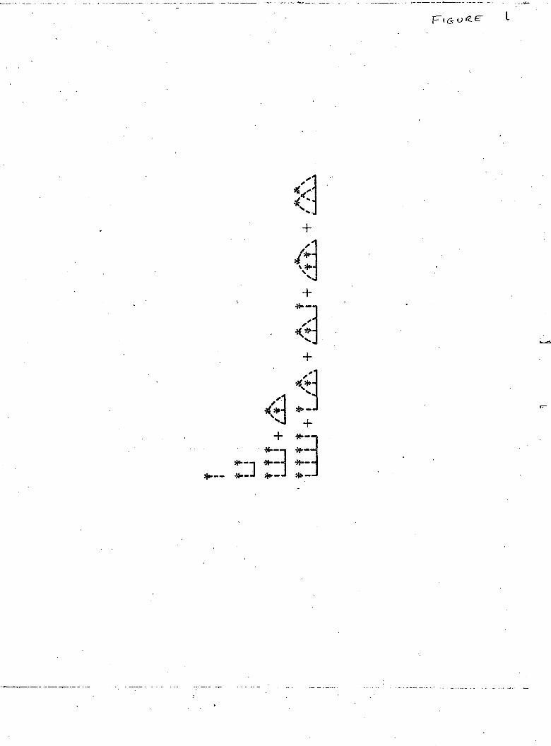
V+
*•—
#-—I #•:] t::
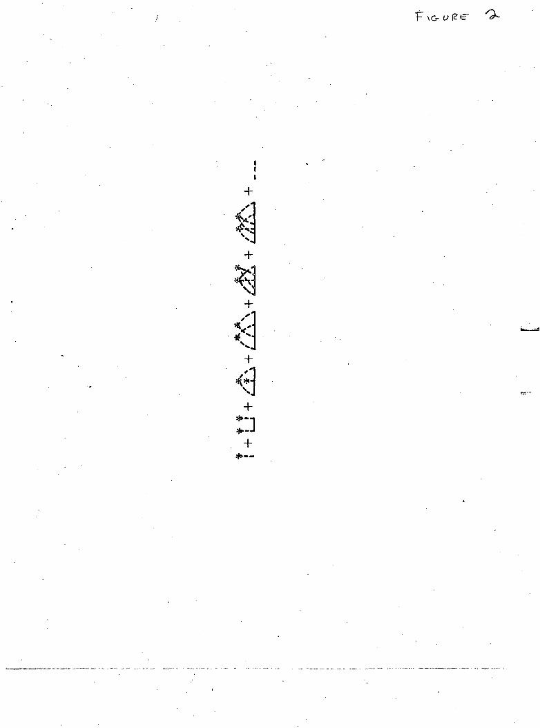
V
*"]*•« '
F \G-
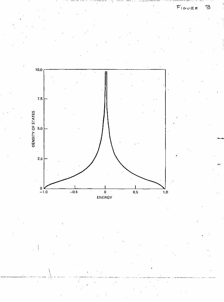
10.0
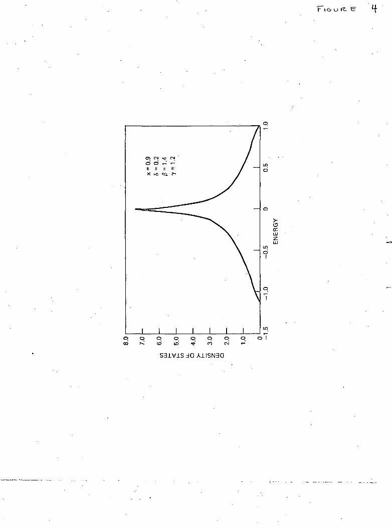
LOo
OccIM
inci
qr—I
q06
qcd
qin
qro
q qCM' i
S31VlSdO A1ISN3Q
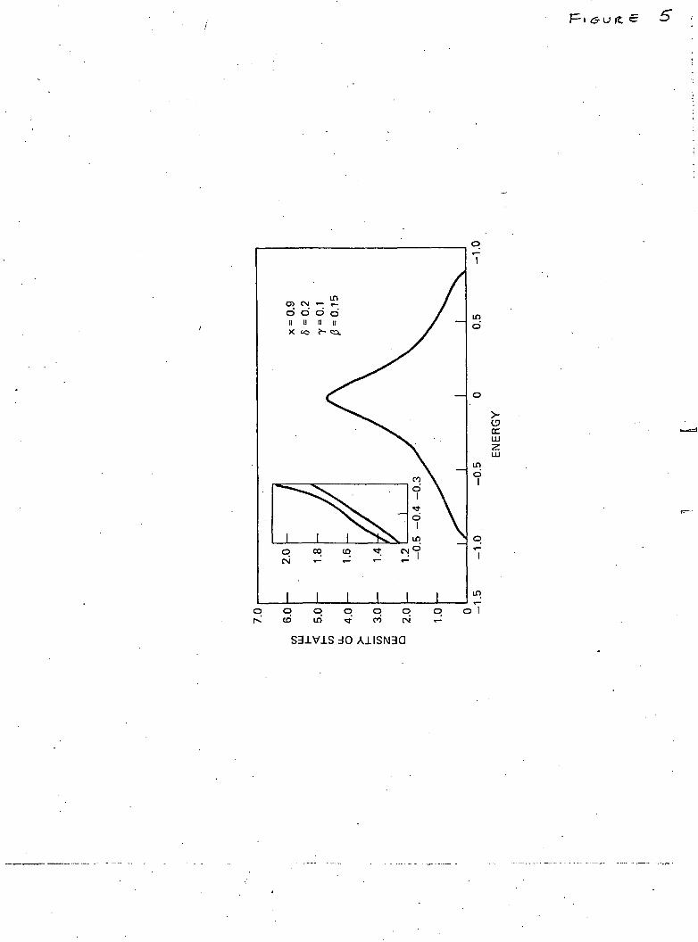
F i & u rt <=•
ino
ccUJ
ind
LO
qcd
qLO
qcri
qCN
o I
S31V1S JO A1ISN3Q
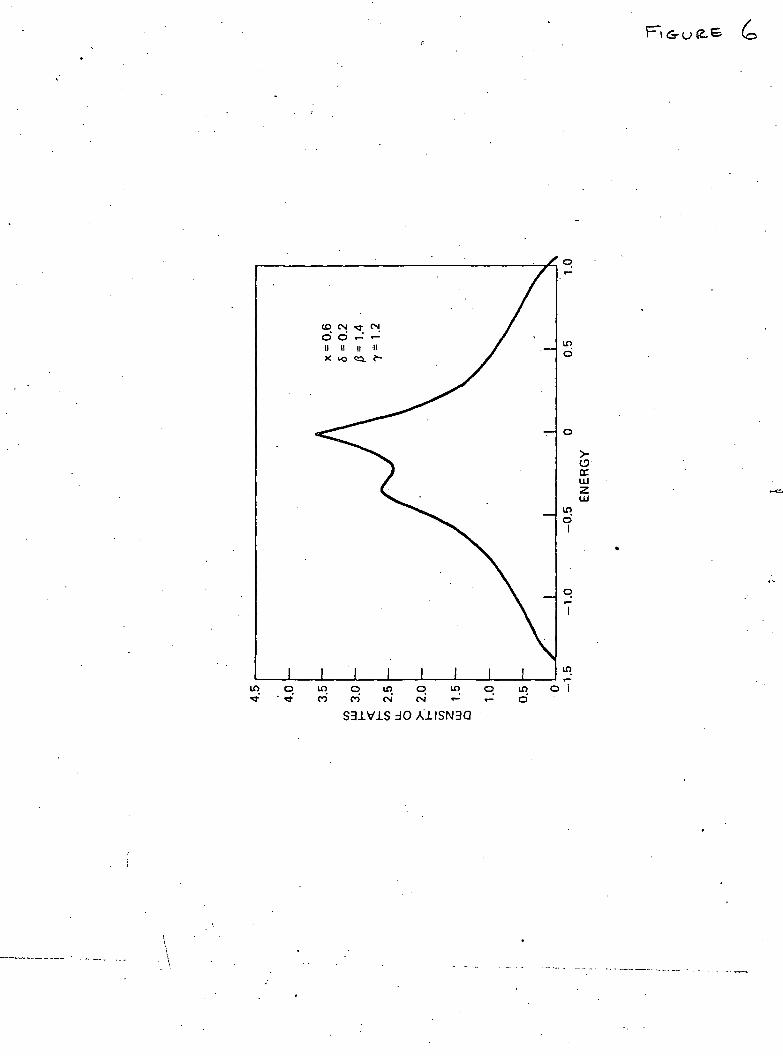
CD CM rj- CMo d «-' •-'II II II IIx
ino
Ooc01z01
ind
in
in inCO
oCO
in p in pCM' «-' T-'
ind
o I
S31V1S dO A1ISN3Q
CO CM <O CO
o d d oii n ii iix to CQ. •?-
ccLU
LU
ino
qT-
I
in pro
in ino
S31V1S dO A1ISN3Q
4.5
4.0
3.5
3.0
2.5
2.0
1.5
1.0
0.5
0-1.5 -1.0 -0.5 0
ENERGY0.5 1.0
O
S3JLV1S dO AJLISN30
FIG-O (fcC" I O
o>cc
-1.0 -
-2.0 -
-2.5 - -2.3 -2.2 k -2.1
ENERGY
-2.0 -1.9 -1.8
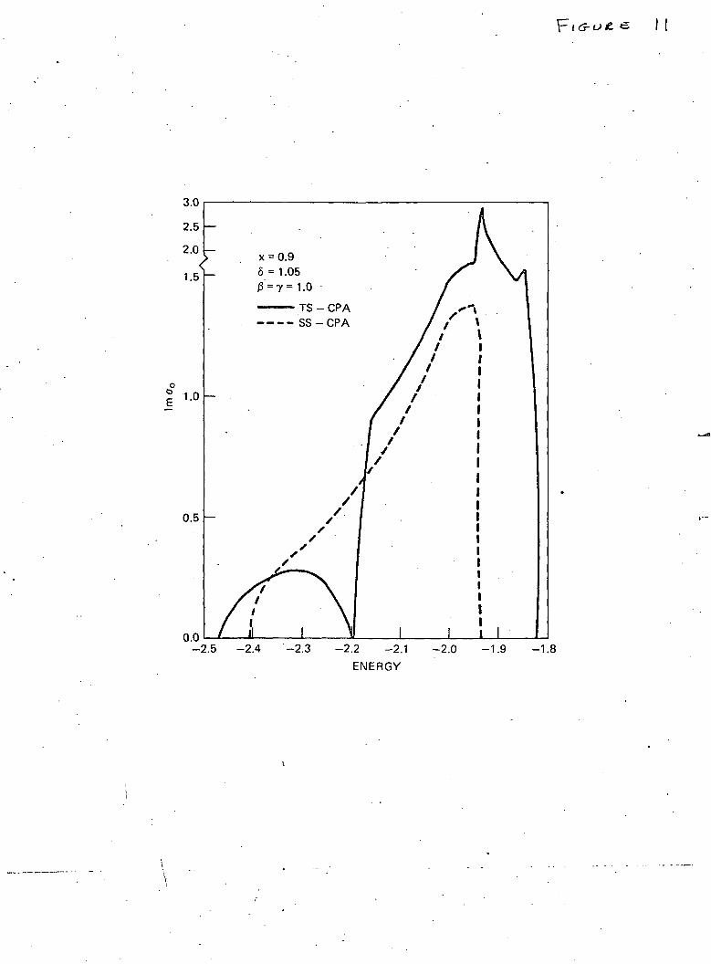
3.0
2.5
2.0
1.5
oto
1.0
0.5
0.0-2.5
x = 0.95 = 1.050 = 7=1.0
TS-CPASS-CPA
-2.4 -2.3 -2.2 -2.1
ENERGY
-2.0 -1.9 -1.8
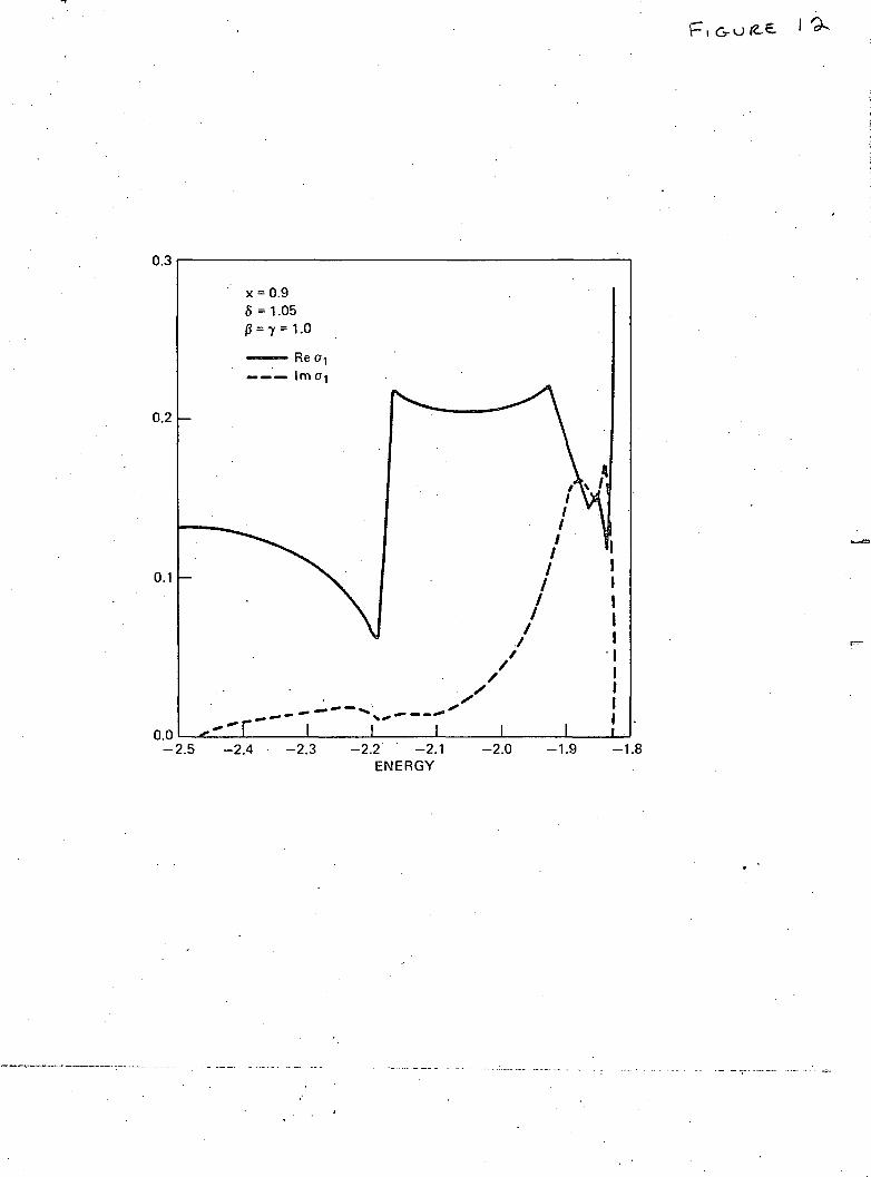
F
0.3
x = 0.96 = 1.05(3 = 7= 1.0
0.2
0.1
0.0-2.5 -2.4 -2.3 -2.2 -2.1
ENERGY-2.0 -1.9 -1.8
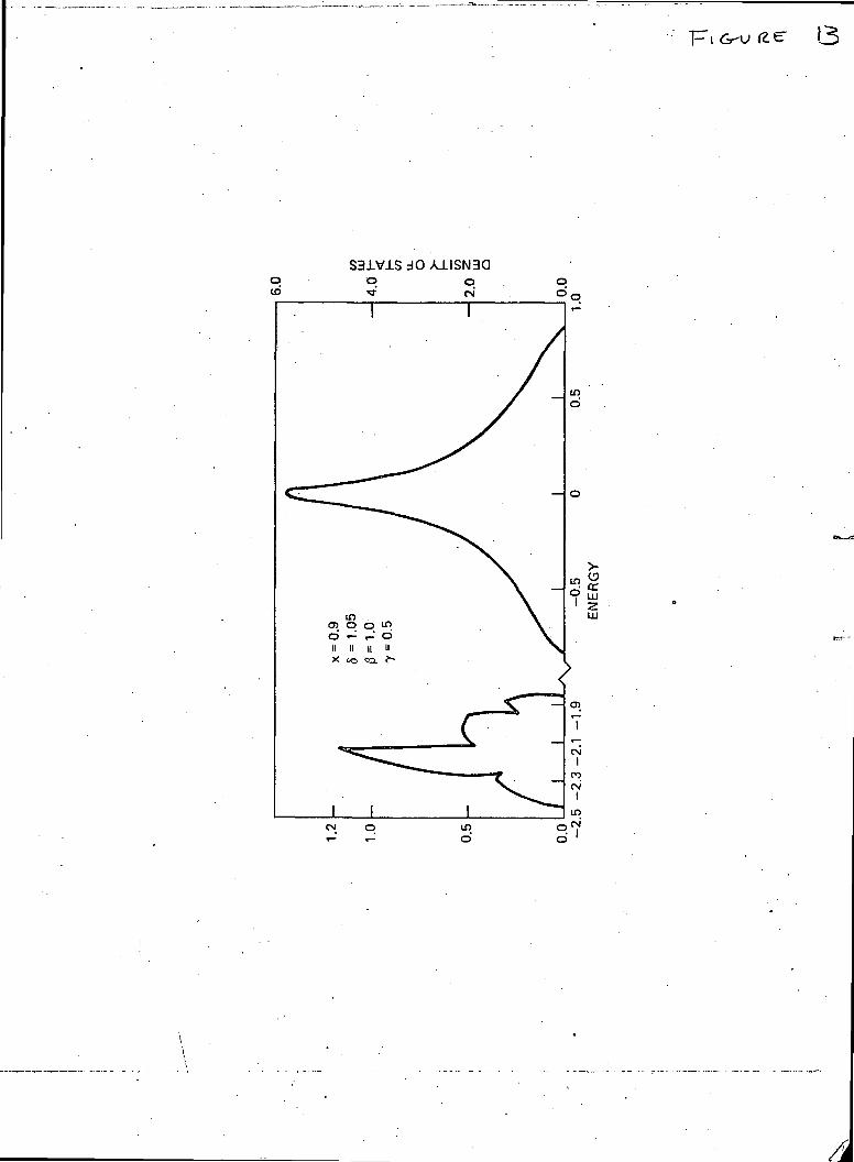
13
qCD
S31V1S dO A1ISN3Qo o
*