Doping and Silicon Reference: Chapter 4 Jaeger or …glennc/e495/e495l6l.pdfFormation of PN Junction...
37
Doping and Silicon Reference: Chapter 4 Jaeger or Chapter 3 Ruska Recall dopants in silicon (column IV element) Column V extra electrons N type dopant N D P Phospherus, As Arsenic & Sb Antimony most common Column III holes (missing e’s) Acceptors P type dopant N A B Boron, Al Aluminum most common For Diodes and transistors need to make P and N junctions Doping is inserting the impurities into the substrate
-
Upload
hoangkhanh -
Category
Documents
-
view
224 -
download
4
Transcript of Doping and Silicon Reference: Chapter 4 Jaeger or …glennc/e495/e495l6l.pdfFormation of PN Junction...

Doping and Silicon Reference: Chapter 4 Jaeger or Chapter 3 Ruska
Recall dopants in silicon (column IV element) Column V extra electrons N type dopant ND P Phospherus, As Arsenic & Sb Antimony most common Column III holes (missing e’s) Acceptors P type dopant NA B Boron, Al Aluminum most common For Diodes and transistors need to make P and N junctions Doping is inserting the impurities into the substrate
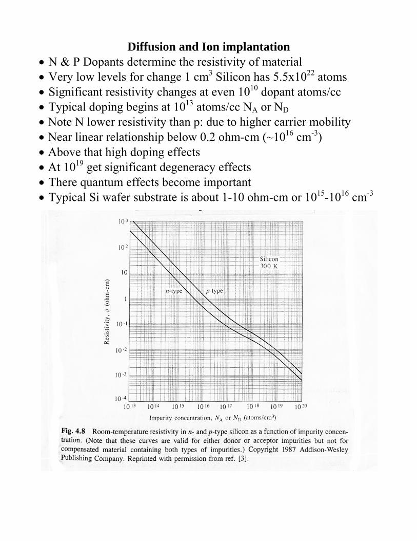
Diffusion and Ion implantation N & P Dopants determine the resistivity of material Very low levels for change 1 cm3 Silicon has 5.5x10²² atoms Significant resistivity changes at even 1010 dopant atoms/cc Typical doping begins at 1013 atoms/cc NA or ND Note N lower resistivity than p: due to higher carrier mobility Near linear relationship below 0.2 ohm-cm (~1016 cm-3) Above that high doping effects At 1019 get significant degeneracy effects There quantum effects become important Typical Si wafer substrate is about 1-10 ohm-cm or 1015-1016 cm-3

Diffusion and Dopant Location Dopping is adding impurities to Silicon Thermal diffusion process easiest Directly implanting (injecting) more expensive Dopant Atoms Substitutional – replaces Si: Called activated dopants – ie n and p carriers created Interstitial dopant: pushes out Si True Interstitial dopant atoms: not activated – no carriers

Diffusion under Concentration Gradient Dopant moves from heavy concentration area to lower concentration area Reason: simple statistics of motion: More dopant in heavy area Hence more heading in lower dopant direction Higher the temperature the faster dopants move Hence for doping done in a furnace

Diffusion Theory Reference: Chapter 4 Jaeger or Chapter 3 Ruska
Diffusion equations for the flux of dopants into the substrate Diffusion flow follows Fick's First Law
),(),(
txNDx
txNDJ
Where: N = Impurity concentration: atoms/cc J = particle flux (atoms/cc/sec) D = diffusion coefficient (cm2/sec) Continuity Equation Now relate the flux to the changes in time and position of dopant Continuity Equation: Fick's Second Law
NDx
)t,x(ND
x
)t,x(ND
xx
J
t
N 22
2
Where: t = time This is the Diffusion differential equation in 1 dimension Assumption is that D is constant with x

Diffusion Solutions Solutions depend on Boundary Conditions Solutions in terms of Dt (Diffusion coef x time) Two typical cases depending on the source conditions Constant Source Diffusion Constant source one common condition: ie unlimited dopant
Dt
x erfcN t)N(x, 0 2
Total impurity concentration
Dt
NdxtxNQ
0
02),(
Limited Source Diffusion Total Dopant is fixed
2
2 Dt
xexp
Dt
Q)t,x(N

Constant Source Diffusion Solutions Constant source one common condition: ie unlimited dopant Surface concentration is fixed for all diffusion time
Dt
x erfcN t)N(x, 0 2
Note this involves the Complementary Error Function Total impurity concentration
Dt
NdxtxNQ
0
02),(

Useful Error Function erfc(x) Approximations Error function erf(x), Complementry Error Function erfc(x) are
dsexerfx
s 0
22)(
dsexerfxerfcx
s
22
)(1)(
erf(x) hard to find but easy to approximate with
233
2211 xetatata)x(erf
47047.01
1
pwhere
pxt
a1 = 0.3480242, a2 = -0.0958798, a3 = 0.7478556 See Abramowitz & Segun (Handbook of Mathematical Functions) Error on this is < 2.5x10⁻⁵ for all x (<2% error for x << 5.5) We are using complementary error function
erfc(x) = 1 - erf(x) erfc(0) = 1 erfc() = 0
Asymptotic approximation
xasx2
11
x
e)x(erfc 2
x2
For x>3.5 this has <1% error (use plot page following for x<3.5) Excel & Quatropro spreadsheet have erf and erfc built in. Must activate analysis toolpack & solver first but become inaccurate for x>5.4 – then use asymptotic Matlab & maple OK for higher x’s For x > 5.4 then ierfc(x) becomes
xasx2
e)x(ierfc 2
x2

Limited Source Diffusion Solutions Where total dopant is fixed Surface dopant falls with time while dopant goes deeper
2
2 Dt
xexp
Dt
Q)t,x(N
Often do constant source first (high concentration very shallow) Then drive in deeper using limited source

Comparison of Normalized Gaussian & ERFC erfc(x) much steeper than Gaussian: thus sharper boundry For erfc use plot for x<3.5, asymptotic formula for > 3.5 Use for getting inverse of erfc Use asymptotic eqn for inverse values of erfc(x)<10-6

Diffusion Constants in Si For common dopants: Change with temperature Follows Arrhenius Formula (EA = activation energy of diffusion)
KT
EexpDD A
0
EA = activation energy of diffusion

Diffusion Constants in Si High diffusion coef D for poisons: Cu, Au, Fe & Li
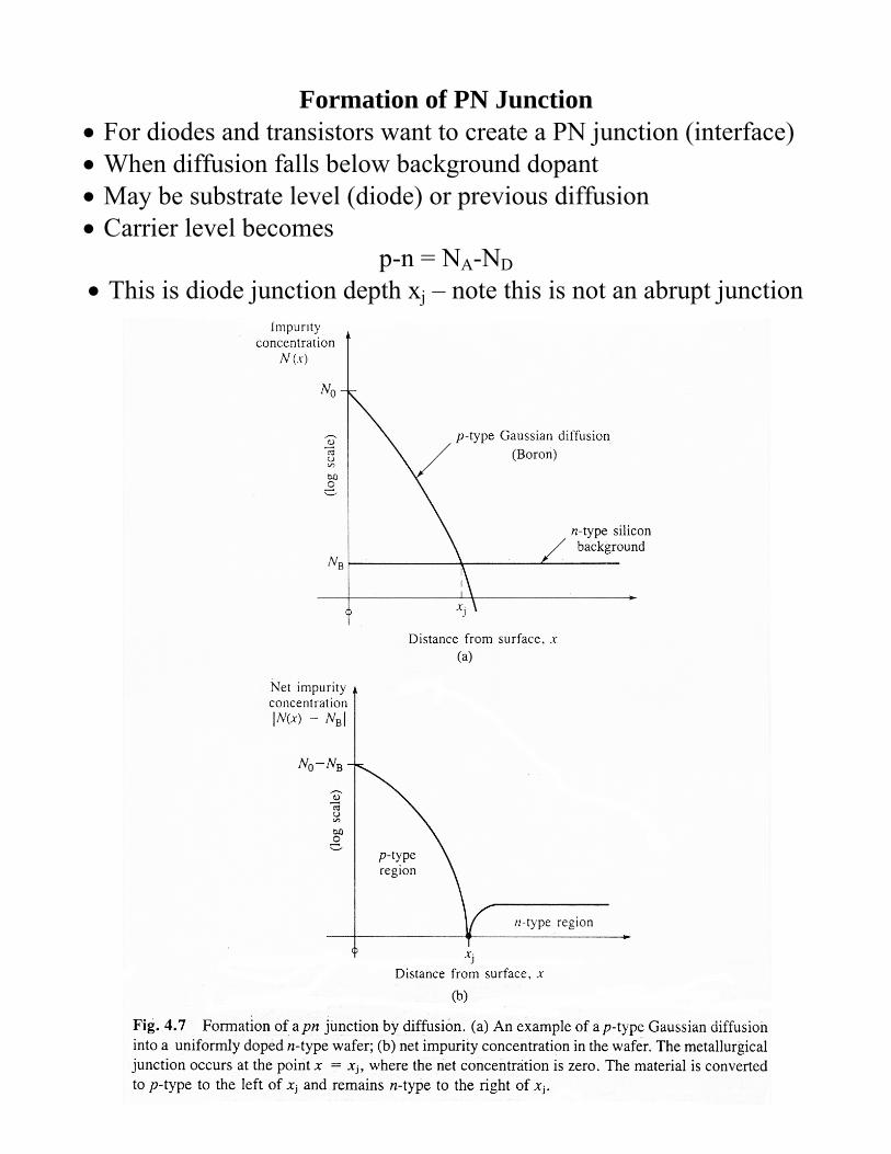
Formation of PN Junction For diodes and transistors want to create a PN junction (interface) When diffusion falls below background dopant May be substrate level (diode) or previous diffusion Carrier level becomes
p-n = NA-ND
This is diode junction depth xj – note this is not an abrupt junction
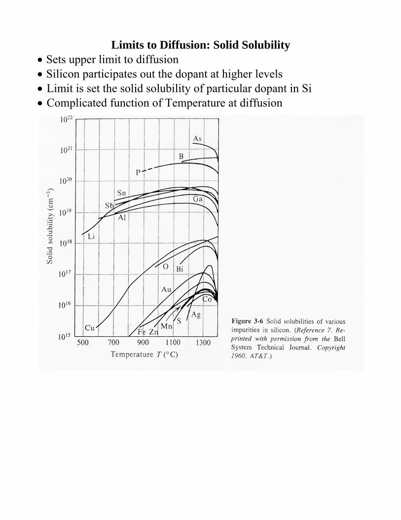
Limits to Diffusion: Solid Solubility Sets upper limit to diffusion Silicon participates out the dopant at higher levels Limit is set the solid solubility of particular dopant in Si Complicated function of Temperature at diffusion

Common Process: Predeposition & Drive in Use diffusion to create thin layer of highly doped material Then drive in dopant from this layer as limited source at surface

Dopant And Masks Commonly use patterned layer (oxide mostly) as mask Hence grow oxide, pattern with resist, etch oxide, strip for mask Then diffuse dopant at high temp (too high for resist) Dopant diffuses under mask

Dopant Diffusion Under Mask Under mask diffusion depends on type: Constant or limited source
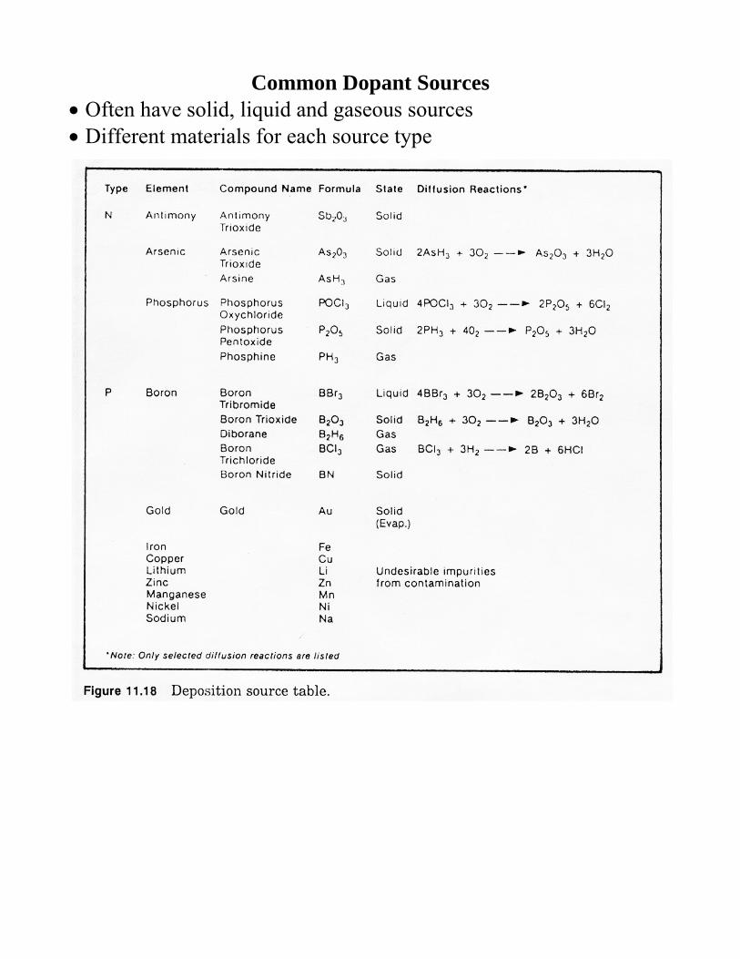
Common Dopant Sources Often have solid, liquid and gaseous sources Different materials for each source type
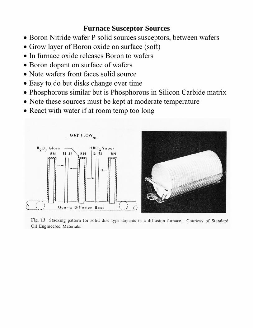
Furnace Susceptor Sources Boron Nitride wafer P solid sources susceptors, between wafers Grow layer of Boron oxide on surface (soft) In furnace oxide releases Boron to wafers Boron dopant on surface of wafers Note wafers front faces solid source Easy to do but disks change over time Phosphorous similar but is Phosphorous in Silicon Carbide matrix Note these sources must be kept at moderate temperature React with water if at room temp too long

Gas Dopant Sources Dopant containing gas flows over wafer Usually have a carrier gas (nitrogen) Dangerous gas product output

Bubbler Dopant Souce Use gas or liquid dopant in bubbler to furnace

Safety and Dopant Sources Common sources very deadly Measure exposure limit for 8 hours in parts per million (ppm)

Uniformity of Dopant Distribution Variation with Vapour source Dopants Doping level varies with gas flow Note variation with flow direction
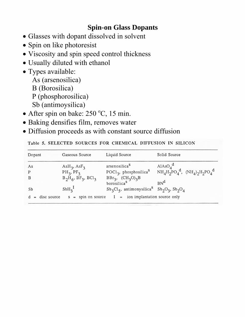
Spin-on Glass Dopants Glasses with dopant dissolved in solvent Spin on like photoresist Viscosity and spin speed control thickness Usually diluted with ethanol Types available: As (arsenosilica) B (Borosilica) P (phosphorosilica) Sb (antimoysilica) After spin on bake: 250 oC, 15 min. Baking densifies film, removes water Diffusion proceeds as with constant source diffusion

Sheet Resistance Definition First measure of doped region is the change in resistivity Sheet resistance used for thin films or layers Measure resistance in Ohms per square Typically put in a test (unprocessed) wafer at that doping process Use these monitor wafers for sheet resistance during processing
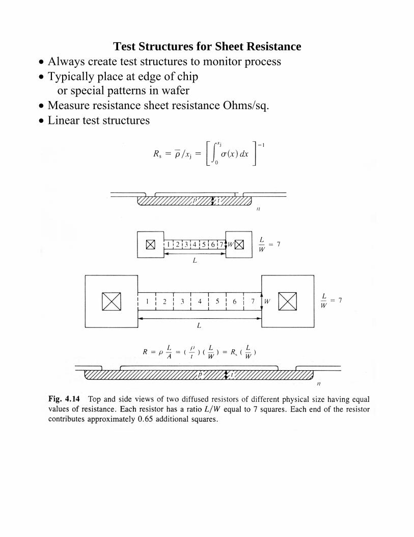
Test Structures for Sheet Resistance Always create test structures to monitor process Typically place at edge of chip or special patterns in wafer Measure resistance sheet resistance Ohms/sq. Linear test structures

Estimating Resistance Often state size of structure in terms of squares Thus for metal contact to diffusion pads get

Surface Dopant Density vs Junction Depth Relationship between junction depth, Background NB and surface dopant concentration N0 Different charts for Constant and Limited source, n & p type

4 Point Probe Sheet Resistance Measurement Test structures often not measureable during processing Instead use 4 point probe stations Use 2 current sources, separate from V measurement Thus do not get resistive loss in measurement Use on test wafers Convert 4 point resistance R to sheet resistance Rs (Ω/)
ln 24.53

Common Resistance Test Structure: Van der Pauw 4 point probe type test structure for post fabrication tests Need to add metallization contacts first Measures sheet resistance
4 point structures on lab wafers – two for p and n dopants

Angle Lapping: Stain Measurement of Junction thickness For all doping need to determine dopant depth/profile For diodes/transistors junction depth important process Typically put in a test (unprocessed) wafer at that doping process Lap (grind away) test wafer at shallow angle (< 2o) After lapping stain the wafer to identify dopant Staining N type Junction Place drop of copper suphate (CuSO4) junction Illuminate junction with intense light (UV best) causes junction to forward bias Voltage causes Cu++ to plate on n side

Interference Technique for Grove Angle lap & stain wafers Place Glass slide over wafer Illuminate with single wavelength light laser or sodium vapour light Get optical interference creating lines at half wavelength Junction depth by counting lines
2
Ntandx j

Cylinder Grove of Junctions To get shallow angle use a rotating cylinder Grove & stain, then measure linear distance Depth calculated as below

Advanced Techniques for Dopant Measurement

Make shallow angle grove (few degrees) Allows a slow change across diffusion layers 1 deg angle causes 1 m depth to become 57 m wide layer Now use 4 point probe resistance method across width of grove Good for junctions greater than 1 microns Gives junction profiles

Secondary Ion Mass Spectrometry (SIMS) Bombard surface in vacuum with ions (1-20 KeV) Nocks atoms off surface (sputtering) Sputtered atoms collect in Mass Spectrometer Count the number of atoms with specific charge/mass ratio Si different than dopants Can sputter down depth of sample measuring ratios Get a depth versus dopant profile Can map the dopants vs position Expensive: about $500/$1000 per profile

Scanning Ion Microscopy (SMIS) Get 2D map of dopant profile Expensive: about $1000 per profile Great for complex 2D structures