EVALUATION KIT AVAILABLE Dual RF LDMOS Bias …€¦ · · 2009-02-06The MAX11008 controller...
67
General Description The MAX11008 controller biases RF LDMOS power devices found in cellular base stations and other wire- less infrastructure equipment. Each controller includes a high-side current-sense amplifier with programmable gains of 2, 10, and 25 to monitor the LDMOS drain cur- rent over a range of 20mA to 5A. The MAX11008 sup- ports up to two external diode-connected transistors to monitor the LDMOS temperatures while an internal tem- perature sensor measures the local die temperature. A 12-bit successive-approximation register (SAR) analog- to-digital converter (ADC) converts the analog signals from the programmable-gain amplifiers (PGAs), exter- nal temperature sensors, internal temperature measure- ment, and two additional auxiliary inputs. The MAX11008 automatically adjusts the LDMOS bias volt- ages by applying temperature, AIN, and/or drain cur- rent samples to data stored in lookup tables (LUTs). The MAX11008 includes two gate-drive channels, each consisting of a 12-bit DAC to generate the positive gate voltage for biasing the LDMOS devices. Each gate- drive output supplies up to ±2mA of gate current. The gate-drive amplifier is current-limited to ±25mA and features a fast clamp to AGND. The MAX11008 contains 4Kb of on-chip, nonvolatile EEPROM organized as 256 bits x 16 bits to store LUTs and register information. The device operates from either a 4-wire 16MHz SPI™-/MICROWIRE™-compati- ble or an I 2 C-compatible serial interface. The MAX11008 operates from a +4.75V to +5.25V ana- log supply with a typical supply current of 2mA, and a +2.7V to +5.25V digital supply with a typical supply of 3mA. The device is packaged in a 48-pin, 7mm x 7mm, thin QFN package and operates over the extended (-40°C to +85°C) temperature range. Applications Cellular Base Stations Microwave Radio Links Feed-Forward Power Amps Transmitters Industrial Process Control Features ♦ On-Chip 4Kb EEPROM for Storing LDMOS Bias Characteristics ♦ Integrated High-Side Current-Sense PGA with Gain of 2, 10, or 25 ♦ ±0.75% Accuracy for Sense Voltage Between +75mV and +1250mV ♦ Full-Scale Sense Voltage +100mV with a Gain of 25 +250mV with a Gain of 10 +1250mV with a Gain of 2 ♦ Common-Mode Range, LDMOS Drain Voltage: +5V to +32V ♦ Adjustable Low-Noise 0 to AV DD Output Gate Bias Voltage Range ♦ Fast Clamp to AGND for LDMOS Protection ♦ 12-Bit DAC Control of Gate with Temperature ♦ Internal Die Temperature Measurement ♦ 2-Channel External Temperature Measurement through Remote Diodes ♦ Internal 12-Bit ADC Measurement for Temperature, Current, and Voltage Monitoring ♦ User-Selectable Serial Interface 400kHz/1.7MHz/3.4MHz I 2 C-Compatible Interface 16MHz SPI-/MICROWIRE-Compatible Interface MAX11008 Dual RF LDMOS Bias Controller with Nonvolatile Memory ________________________________________________________________ Maxim Integrated Products 1 19-4371; Rev 0; 11/08 For pricing, delivery, and ordering information, please contact Maxim Direct at 1-888-629-4642, or visit Maxim’s website at www.maxim-ic.com. EVALUATION KIT AVAILABLE SPI is a trademark of Motorola, Inc. MICROWIRE is a trademark of National Semiconductor Corp. Ordering Information PART PIN-PACKAGE TEMP ERROR (°C) MAX11008BETM+ 48 TQFN-EP* ±3 +Denotes a lead-free/RoHS-compliant package. *EP = Exposed pad. Note: The device is specified over the -40°C to +85°C operating temperature range.
Transcript of EVALUATION KIT AVAILABLE Dual RF LDMOS Bias …€¦ · · 2009-02-06The MAX11008 controller...
General DescriptionThe MAX11008 controller biases RF LDMOS powerdevices found in cellular base stations and other wire-less infrastructure equipment. Each controller includesa high-side current-sense amplifier with programmablegains of 2, 10, and 25 to monitor the LDMOS drain cur-rent over a range of 20mA to 5A. The MAX11008 sup-ports up to two external diode-connected transistors tomonitor the LDMOS temperatures while an internal tem-perature sensor measures the local die temperature. A12-bit successive-approximation register (SAR) analog-to-digital converter (ADC) converts the analog signalsfrom the programmable-gain amplifiers (PGAs), exter-nal temperature sensors, internal temperature measure-ment, and two additional auxil iary inputs. TheMAX11008 automatically adjusts the LDMOS bias volt-ages by applying temperature, AIN, and/or drain cur-rent samples to data stored in lookup tables (LUTs).
The MAX11008 includes two gate-drive channels, eachconsisting of a 12-bit DAC to generate the positive gatevoltage for biasing the LDMOS devices. Each gate-drive output supplies up to ±2mA of gate current. Thegate-drive amplifier is current-limited to ±25mA andfeatures a fast clamp to AGND.
The MAX11008 contains 4Kb of on-chip, nonvolatileEEPROM organized as 256 bits x 16 bits to store LUTsand register information. The device operates fromeither a 4-wire 16MHz SPI™-/MICROWIRE™-compati-ble or an I2C-compatible serial interface.
The MAX11008 operates from a +4.75V to +5.25V ana-log supply with a typical supply current of 2mA, and a+2.7V to +5.25V digital supply with a typical supply of3mA. The device is packaged in a 48-pin, 7mm x 7mm,thin QFN package and operates over the extended(-40°C to +85°C) temperature range.
ApplicationsCellular Base Stations
Microwave Radio Links
Feed-Forward Power Amps
Transmitters
Industrial Process Control
Features♦ On-Chip 4Kb EEPROM for Storing LDMOS Bias
Characteristics
♦ Integrated High-Side Current-Sense PGA withGain of 2, 10, or 25
♦ ±0.75% Accuracy for Sense Voltage Between+75mV and +1250mV
♦ Full-Scale Sense Voltage+100mV with a Gain of 25+250mV with a Gain of 10+1250mV with a Gain of 2
♦ Common-Mode Range, LDMOS Drain Voltage:+5V to +32V
♦ Adjustable Low-Noise 0 to AVDD Output GateBias Voltage Range
♦ Fast Clamp to AGND for LDMOS Protection
♦ 12-Bit DAC Control of Gate with Temperature
♦ Internal Die Temperature Measurement
♦ 2-Channel External Temperature Measurementthrough Remote Diodes
♦ Internal 12-Bit ADC Measurement forTemperature, Current, and Voltage Monitoring
♦ User-Selectable Serial Interface400kHz/1.7MHz/3.4MHz I2C-Compatible Interface16MHz SPI-/MICROWIRE-Compatible Interface
MA
X1
10
08
Dual RF LDMOS Bias Controller withNonvolatile Memory
________________________________________________________________ Maxim Integrated Products 1
19-4371; Rev 0; 11/08
For pricing, delivery, and ordering information, please contact Maxim Direct at 1-888-629-4642,or visit Maxim’s website at www.maxim-ic.com.
EVALUATION KIT
AVAILABLE
SPI is a trademark of Motorola, Inc.
MICROWIRE is a trademark of National Semiconductor Corp.
Ordering Information
PART PIN-PACKAGETEMP
ERROR (°C)
MAX11008BETM+ 48 TQFN-EP* ±3
+Denotes a lead-free/RoHS-compliant package.*EP = Exposed pad.
Note: The device is specified over the -40°C to +85°C operatingtemperature range.
MA
X1
10
08
Dual RF LDMOS Bias Controller withNonvolatile Memory
2 _______________________________________________________________________________________
ABSOLUTE MAXIMUM RATINGS
ELECTRICAL CHARACTERISTICS(VCS_+ = +32V, AVDD = DVDD = +5V ±5%, external VREFADC = +2.5V, external VREFDAC = +2.5V, CREF = 0.1µF, CGATE_ = 0.1nF,VSENSE = VCS_+ - VCS_-, TA = -40°C to +85°C, unless otherwise noted. Typical values are at TA = +25°C.)
Stresses beyond those listed under “Absolute Maximum Ratings” may cause permanent damage to the device. These are stress ratings only, and functionaloperation of the device at these or any other conditions beyond those indicated in the operational sections of the specifications is not implied. Exposure toabsolute maximum rating conditions for extended periods may affect device reliability.
AVDD to AGND .........................................................-0.3V to +6VDVDD to DGND.........................................................-0.3V to +6VAGND to DGND.....................................................-0.3V to +0.3VCS_+, CS_- to AGND .............................................-0.3V to +34VCS_+ to CS_-
If CS_+ > 6V .........................................................-0.3V to +6VIf CS_+ ≤ 6V .......................................................-0.3V to VCS_-
Analog Inputs/Outputs to AGND.............................................................................-0.3V to the lower of (AVDD + 0.3V) and +6V
Digital Inputs/Outputs to DGND(except SDA/DIN and SCL/SCLK)........................................................................-0.3V to the lower of (DVDD+ 0.3V) and +6V
SDA/DIN and SCL/SCLK to DGND ..........................-0.3V to +6VContinuous Input Current (all terminals)...........................±50mAContinuous Power Dissipation (TA = +70°C)
48-Pin, 7mm x 7mm, TQFN (derate 27.8mW/°C above+70°C).....................................................................2222.2mW
Operating Temperature Range ...........................-40°C to +85°CJunction Temperature ......................................................+150°CStorage Temperature Range .............................-65°C to +150°CLead Temperature (soldering, 10s) .................................+300°C
PARAMETER SYMBOL CONDITIONS MIN TYP MAX UNITS
HIGH-SIDE CURRENT-SENSE PGA
Common-Mode Input VoltageRange
VCS1+,VCS2+
5 32 V
Common-Mode Rejection Ratio CMRR 5V < VCS_+ < 32V 110 dB
CS_+ Input Bias Current ICS_+VSENSE < 100mV over the common-moderange
135 195 µA
CS_- Input Bias Current ICS_-VSENSE < 100mV over the common-moderange
±1 µA
Gain = 25 0 100
Gain = 10 0 250Full-Scale Sense Voltage Range VSENSE
Gain = 2 0 1250
mV
Gain = 25 75 100
Gain = 10 75 250Minimum Sense Voltage Rangefor ±0.75% VSENSE Accuracy
Gain = 2 75 1250
mV
Gain = 25 20 100
Gain = 10 20 250Minimum Sense Voltage Rangefor ±2.5% VSENSE Accuracy
Gain = 2 20 1250
mV
Total PGAOUT Voltage Error VSENSE = 75mV ±0.1 ±0.75 %
PGAOUT Capacitive Load CPGAOUT 50 pF
PGAOUT Settling Time tHSCS (Note 1) < 25 µs
Saturation Recovery TimeSettles to within ±0.5% accuracy fromVSENSE = 3 x full scale
< 45 µs

MA
X1
10
08
Dual RF LDMOS Bias Controller withNonvolatile Memory
_______________________________________________________________________________________ 3
PARAMETER SYMBOL CONDITIONS MIN TYP MAX UNITS
LDMOS GATE DRIVER (Gain = 2)
IGATE_ = ±0.1mA 0.1AVDD -
0.1Output Gate-Drive Voltage Range VGATE_
IGATE_ = ±2mA 0.75AVDD -
0.75
V
Output Impedance RGATE_ Measured at DC 0.1 Ω
GATE_ Settling Time tGATE_RS = 500Ω, CGATE_ = 15µF, VGATE_ =0.5V to 4.5V (Note 1)
45 ms
RSERIES = 0Ω 0 0.5Output Capacitive Load CGATE_
RSERIES = 500Ω 0 15,000nF
GATE_ Noise 1kHz to 1MHz 1000 µVP-P
Maximum Power-On Transient ±100 mV
Output Short-Circuit Current Limit ISC 1s, sinking or sourcing ±25 mA
Total Unadjusted Error TUEWorst case at CODE = 4063, useexternal reference (Note 2)
±7 ±25 mV
Total Unadjusted Error withoutOffset
TUENO_OFFSET
CalCODE = 2457, MaxCODE = 2867,use external reference, TA = +25°C(Note 2)
±8 mV
Drift Gain = 2, MaxCODE = 2867 (Note 2) ±15 µV/°C
Clamp to Zero Delay CGATE_ = 0.5nF (Note 3) 1 µs
Output-Safe Switch On-Resistance
ROPSW VGATE_ clamped to AGND (Note 4) 300 Ω
MONITOR ADC (DC characteristics)
Resolution NADC 12 Bits
Differential Nonlinearity DNLADC (Note 5) -2 +2 LSB
Integral Nonlinearity INLADC ±2 LSB
Offset Error ±2 ±4 LSB
Gain Error (Note 6) ±2 ±4 LSB
Gain Temperature Coefficient ±0.4 ppm/°C
Offset Temperature Coefficient ±0.4 ppm/°C
MONITOR ADC DYNAMIC CHARACTERISTICS (1kHz sine-wave input, 2.5VP-P, up to 94.4ksps)
Signal-to-Noise Plus Distortion SINAD 70 dB
Total Harmonic Distortion THD Up to 5th harmonic -82 dBc
Spurious-Free Dynamic Range SFDR 86 dBc
Intermodulation Distortion IMD fIN1 = 0.99kHz, fIN2 = 1.02kHz 76 dBc
Full-Power Bandwidth -3dB 1 MHz
Full-Linear Bandwidth SINAD > 68dB 100 kHz
ELECTRICAL CHARACTERISTICS (continued)(VCS_+ = +32V, AVDD = DVDD = +5V ±5%, external VREFADC = +2.5V, external VREFDAC = +2.5V, CREF = 0.1µF, CGATE_ = 0.1nF,VSENSE = VCS_+ - VCS_-, TA = -40°C to +85°C, unless otherwise noted. Typical values are at TA = +25°C.)

MA
X1
10
08
Dual RF LDMOS Bias Controller withNonvolatile Memory
4 _______________________________________________________________________________________
ELECTRICAL CHARACTERISTICS (continued)(VCS_+ = +32V, AVDD = DVDD = +5V ±5%, external VREFADC = +2.5V, external VREFDAC = +2.5V, CREF = 0.1µF, CGATE_ = 0.1nF,VSENSE = VCS_+ - VCS_-, TA = -40°C to +85°C, unless otherwise noted. Typical values are at TA = +25°C.)
PARAMETER SYMBOL CONDITIONS MIN TYP MAX UNITS
MONITOR ADC CONVERSION RATE
Power-Up Time (ExternalReference)
tPUEXT 1.1 µs
Power-Up Time (InternalReference)
tPUINT 70 µs
Acquisition Time tACQ 0.5 µs
Conversion Time tCONV Internally clocked, TA = +25°C 10 µs
Aperture Delay tAD 20 ns
MONITOR ADC ANALOG INPUT (ADCIN1, ADCIN2)
Input Voltage Range VADCIN Relative to AGND (Note 7) 0 VREFADC V
Input Leakage Current VIN = 0 and VIN = VAVDD ±0.01 µA
Input Capacitance CADCIN 34 pF
TEMPERATURE MEASUREMENTS
TA = +25°C ±0.25Internal Sensor MeasurementError TA = TMIN to TMAX (Note 8) ±1.5 ±3
°C
TA = +25°C ±1External Sensor MeasurementError (Note 9) TA = TMIN to TMAX ±3
°C
Relative Temperature Accuracy TA = TMIN to TMAX (Note 9) ±0.4 °C
Temperature Resolution 1/8 °C/LSB
E xter nal D i od e D r i ve C ur r ent ( Low ) 3.25 4 µA
E xter nal D i od e D r i ve C ur r ent ( H i g h) 68 75 µA
INTERNAL REFERENCE
REFADC/REFDAC OutputVoltage
VREFADC,VREFDAC
TA = +25°C 2.49 2.50 2.51 V
REFADC/REFDAC TemperatureCoefficient
TCREFADC,TCREFDAC
±15 ppm/°C
REFADC/REFDAC OutputImpedance
6.5 kΩ
Capacitive Bypass atREFADC/REFDAC
270 pF
Power-Supply Rejection Ratio PSRR AVDD = 5V ± 5% 64 dB
EXTERNAL REFERENCE
REFADC Input Voltage Range VREFADC 1.0 AVDD V
VREFADC = 2.5V, fSAMPLE = 100ksps 60 80REFADC Input Current IREFADC
Acquisition/between conversions ±0.01µA
REFDAC Input Voltage Range VREFDAC 0.7 2.5 V
REFDAC Input Current S tati c cur r ent w hen the D AC i s not cal i b r ated 0.1 µA

MA
X1
10
08
Dual RF LDMOS Bias Controller withNonvolatile Memory
_______________________________________________________________________________________ 5
ELECTRICAL CHARACTERISTICS (continued)(VCS_+ = +32V, AVDD = DVDD = +5V ±5%, external VREFADC = +2.5V, external VREFDAC = +2.5V, CREF = 0.1µF, CGATE_ = 0.1nF,VSENSE = VCS_+ - VCS_-, TA = -40°C to +85°C, unless otherwise noted. Typical values are at TA = +25°C.)
PARAMETER SYMBOL CONDITIONS MIN TYP MAX UNITS
GATE-DRIVER DAC DC ACCURACY
Resolution NDAC 12 Bits
Integral Nonlinearity INLDAC Measured at GATE_ ±2 ±4 LSB
Differential Nonlinearity DNLDAC Guaranteed monotonic (Note 10) ±1 LSBDIGITAL INPUTS (SCL/SCLK, SDA/DIN, A0/CS, A1/DOUT, A2/N.C., CNVST, OPSAFE1, OPSAFE2)
SDA/DIN and SCL/SCLK only0.7 xDVDD
Input High Voltage VIHA0/CS, A1/DOUT, A2/N.C., CNVST,OPSAFE1, OPSAFE2 only
2.3
V
SDA/DIN and SCL/SCLK only0.3 xDVDD
Input Low Voltage VILA0/CS, A1/DOUT, A2/N.C., CNVST,OPSAFE1, OPSAFE2 only
0.7
V
Input Hysteresis VHYS SDA/DIN and SCL/SCLK only0.08 xDVDD
V
Input Leakage Current Digital inputs at 0 or VDVDD ±0.1 ±1 µA
Input Capacitance CIN 5 pF
DIGITAL OUTPUTS (SDA/DIN, ALARM, BUSY, DOUT)
Output High Voltage VOH ALARM and BUSY only, ISOURCE = 0.2mADVDD- 0.4V
V
SDA/DIN and A1/DOUT, ISINK = 3mA,(Note 11)
0.4Output Low Voltage VOL
ALARM and BUSY only, ISINK = 0.3mA 0.3
V
Three-State Leakage IIL Digital inputs at 0 or DVDD ±0.1 ±1 µA
Three-State Capacitance 5 pF
POWER SUPPLIES (Note 12)
Analog Supply Voltage Range AVDD 4.75 5.25 V
Digital Supply Voltage Range DVDD 2.7AVDD+ 0.3
V
AVDD = 5V 2 4 mAAnalog Supply Current IAVDD
Shutdown (Note 13) 0.4 2 µA
DVDD = 5V 3 6 mADigital Supply Current IDVDD
Shutdown 2 32 µA

MA
X1
10
08
Dual RF LDMOS Bias Controller withNonvolatile Memory
6 _______________________________________________________________________________________
SPI TIMING CHARACTERISTICS (Notes 14, 15, Figure 1)(DVDD = +2.7V to +5.25V, AVDD = +4.75V to +5.25V, VDGND = VAGND = 0, external VREFADC = +2.5V, external VREFDAC = +2.5V,CREF = 0.1µF, TA = -40°C to +85°C, unless otherwise noted.)
PARAMETER SYMBOL CONDITIONS MIN TYP MAX UNITS
SCLK Clock Period tCP 62.5 ns
SCLK High Time tCH 25 ns
SCLK Low Time tCL 25 ns
DIN to SCLK Rise Setup Time tDS 15 ns
DIN to SCLK Rise Hold Time tDH 0 ns
SCLK Fall to DOUT Transition tDO CL = 30pF 20 ns
CS Fall to DOUT Enable tDV CL = 30pF 50 ns
CS Rise to DOUT Disable tTR CL = 30pF (Note 16) 50 ns
CS Rise or Fall to SCLK Rise tCSS 12.5 ns
CS Pulse-Width High tCSW 50 ns
Last SCLK Rise to CS Rise tCSH 0 ns
I2C SLOW-/FAST-MODE TIMING CHARACTERISTICS (Notes 14, 15, Figure 4)(DVDD = +2.7V to +5.25V, AVDD = +4.75V to +5.25V, VDGND = VAGND = 0, external VREFADC = +2.5V, external VREFDAC = +2.5V,CREF = 0.1µF, TA = -40°C to +85°C, unless otherwise noted.)
PARAMETER SYMBOL CONDITIONS MIN TYP MAX UNITS
SCL Clock Frequency fSCL 0 400 kHz
Bus Free Time Between a STOPand START Condition
tBUF 1.3 µs
Hold Time (Repeated) for STARTCondition
tHD:STAAfter this period, the first clock pulse isgenerated
0.6 µs
Setup Time for a RepeatedSTART Condition
tSU:STA 0.6 µs
SCL Pulse-Width Low tLOW 1.3 µs
SCL Pulse-Width High tHIGH 0.6 µs
Data Setup Time tSU:DAT 100 ns
Data Hold Time tHD:DAT (Note 17) 0.004 0.9 µs
SDA, SCL Rise Time tR Receiving (Note 18) 0 300 ns
SDA, SCL Fall Time tF Receiving (Note 18) 0 300 ns
SDA Fall Time tF Transmitting (Notes 18, 19)20 + 0.1
x C B 250 ns
Setup Time for STOP Condition tSU:STO 0.6 µs
Capacitive Load for Each BusLine
CB (Note 20) 400 pF
Pulse Width of SpikesSuppressed by the Input Filter
tSP (Note 21) 50 ns

MA
X1
10
08
Dual RF LDMOS Bias Controller withNonvolatile Memory
_______________________________________________________________________________________ 7
I2C HIGH-SPEED-MODE TIMING CHARACTERISTICS (Notes 14, 15, Figure 4)(DVDD = +2.7V to +5.25V, AVDD = +4.75V to +5.25V, VDGND = VAGND = 0, external VREFADC = +2.5V, external VREFDAC = +2.5V,CREF = 0.1µF, TA = -40°C to +85°C, unless otherwise noted.)
CB = 100pF max CB = 400pFPARAMETER SYMBOL CONDITIONS
MIN MAX MIN MAXUNITS
Serial Clock Frequency fSCL 0 3.4 0 1.7 MHzSetup Time (Repeated) STARTCondition
tSU:STA 160 160 ns
Hold Time (Repeated) STARTCondition
tHD:STA 160 160 ns
SCL Pulse-Width Low tLOW 160 320 ns
SCL Pulse-Width High tHIGH 80 120 ns
Data Setup Time tSU:DAT 10 10 ns
Data Hold Time tHD:DAT (Note 17) 4 70 4 150 ns
SCL Rise Time tRCL 10 40 20 80 ns
SCL Rise Time tRCL1
After a repeated STARTcondition and after anacknowledge bit
10 80 20 160 ns
SCL Fall Time tFCL 10 40 20 80 nsSDA Rise Time tRDA 10 80 20 160 ns
SDA Fall Time tFDA 10 80 20 160 ns
Setup Time for STOP Condition tSU:STO 160 160 ns
Capacitive Load for Each Bus Line CB (Note 20) 100 400 ns
Pulse Width of Spikes Suppressedby the Input Filter
tSP (Note 21) 0 10 0 10 ns
MISCELLANEOUS TIMING CHARACTERISTICS (Note 15)(DVDD = +2.7V to +5.25V, AVDD = +4.75V to +5.25V, VDGND = VAGND = 0, external VREFADC = +2.5V, external VREFDAC = +2.5V,CREF = 0.1µF, TA = -40°C to +85°C, unless otherwise noted.)
PARAMETER SYMBOL CONDITIONS MIN TYP MAX UNITS
Minimum Time to Wait After a WriteCommand Before Reading BackData from the Same Location
tRDBK (Note 22) 1 µs
CNVST Active-Low Pulse Width inADC Clock Mode 01
tCNV01 20 ns
CNVST Active-Low Pulse Width inADC Clock Mode 11 to Initiate aTemperature Conversion
tCNV11 20 ns
CNVST Active-Low Pulse Width inADC Clock Mode 11 for ADCIN1/2Acquisition
tACQ11A 1.5 µs
ADC Power-Up Time (ExternalReference)
tAPUEXT 1.1 µs
ADC Power-Up Time (InternalReference)
tAPUINT 70 µs

MA
X1
10
08
Dual RF LDMOS Bias Controller withNonvolatile Memory
8 _______________________________________________________________________________________
MISCELLANEOUS TIMING CHARACTERISTICS (Note 15) (continued)(DVDD = +2.7V to +5.25V, AVDD = +4.75V to +5.25V, VDGND = VAGND = 0, external VREFADC = +2.5V, external VREFDAC = +2.5V,CREF = 0.1µF, TA = -40°C to +85°C, unless otherwise noted.)
PARAMETER SYMBOL CONDITIONS MIN TYP MAX UNITS
DAC Power-Up Time (ExternalReference)
tDPUEXT 2 µs
DAC Power-Up Time (InternalReference)
tDPUINT 70 µs
Acquisition Time (Internally Timedin ADC Clock Modes 00 or 01)
tACQ 0.6 µs
Conversion Time (InternallyClocked)
tCONV Internally clocked, TA = +25°C 10 µs
Delay to Start of Conversion Time tCONVW (Note 23) 1.3 µs
Temperature Conversion Time(Internally Clocked)
tCONVT 70 µs
Note 1: Output settles to within ±0.5% of final value.Note 2: Total unadjusted errors are for the entire gate-drive channel including the 12-bit DAC, and the gate driver is measured at
the GATE1 and GATE2 outputs.Note 3: VGATE_ = VDD - 0.1. Measured from when OPSAFE1 or OPSAFE2 is set high.Note 4: During power-on-reset, the output safe switch is closed. The output safe switch is opened under user software control.Note 5: Guaranteed to be 11 bits linearly accurate.Note 6: Offset nulled.Note 7: The absolute range for analog inputs is from 0 to VAVDD.Note 8: Internal temperature-sensor performance is guaranteed by design.Note 9: The MAX11008 and the external sensor are at the same ambient temperature. External sensor measurement error is tested
with a diode-connected 2N3904.Note 10: Guaranteed monotonicity. Accuracy is degraded at lower VREFDAC.Note 11: SDA/DIN is an open-drain output only when in I2C mode. A1/DOUT is an open-drain output only when in SPI mode. Note 12: Supply-current limits are valid only when digital inputs are set to DGND or supply voltage. Timing specifications are only
guaranteed when inputs are driven rail-to-rail.Note 13: Shutdown supply currents are typically 0.4µA for AVDD; maximum specification is limited by automated test equipment.Note 14: All times are referred to the 50% point between VIH and VIL levels.Note 15: Guaranteed by design. Not production tested.Note 16: DOUT will go into three-state mode after the CS rising edge. Keep CS low long enough for the DOUT value to be sampled
before it goes to three-state.Note 17: A master device must provide a hold time of at least 300ns for the SDA signal (referred to VIL of the SCL signal) to bridge
the undefined region of SCL’s falling edge.Note 18: tR and tF measured between 0.3 x DVDD and 0.7 x DVDD.Note 19: CB = total capacitance of one bus line in pF. For bus loads between 100pF and 400pF, the timing parameters should be
linearly interpolated.Note 20: An appropriate bus pullup resistance must be selected depending on board capacitance.Note 21: Input filters on the SDA and SCL inputs suppress noise spikes less than 50ns.Note 22: When a command is written to the serial interface, the command is passed by the internal oscillator clock and executed.
There is a small synchronization delay before the new value is written to the appropriate register. If the serial interfaceattempts to read the new value back before tRDBK, the new data is not corrupted; however, the result of the read commandmay not reflect the new value.
Note 23: This is the minimum time from the end of a command before CNVST should be asserted. The time allows for the data fromthe preceding write to arrive and set up the chip in preparation for the CNVST. The time need only be observed when thewrite affects the ADC controls. Failure to observe this time may lead to incorrect conversions (for example, conversion ofthe wrong ADC channel).
MA
X1
10
08
Dual RF LDMOS Bias Controller withNonvolatile Memory
_______________________________________________________________________________________ 9
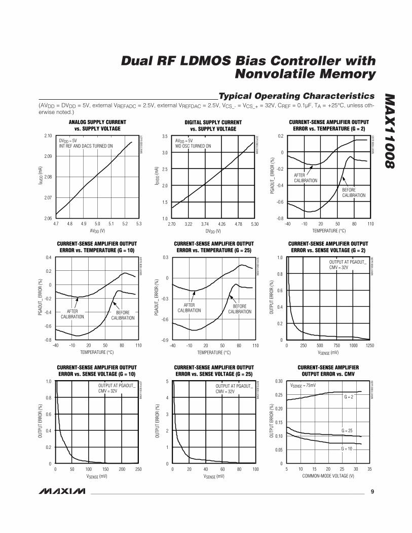
Typical Operating Characteristics(AVDD = DVDD = 5V, external VREFADC = 2.5V, external VREFDAC = 2.5V, VCS_- = VCS_+ = 32V, CREF = 0.1µF, TA = +25°C, unless oth-erwise noted.)
2.06
2.07
2.08
2.09
2.10
4.7 4.94.8 5.0 5.1 5.2 5.3
ANALOG SUPPLY CURRENTvs. SUPPLY VOLTAGE
MAX
1100
8 to
c01
AVDD (V)
I AVD
D (m
A)
DVDD = 5VINT REF AND DACS TURNED ON
1.0
1.5
2.5
2.0
3.0
3.5
2.70 3.743.22 4.26 4.78 5.30
DIGITAL SUPPLY CURRENTvs. SUPPLY VOLTAGE
MAX
1100
8 to
c02
DVDD (V)
I DVD
D (m
A)
AVDD = 5VWD OSC TURNED ON
-0.8
-0.6
-0.2
-0.4
0
0.2
-40 20-10 50 80 110
CURRENT-SENSE AMPLIFIER OUTPUTERROR vs. TEMPERATURE (G = 2)
MAX
1100
8 to
c03
TEMPERATURE (°C)
PGAO
UT_
ERRO
R (%
)
AFTERCALIBRATION
BEFORECALIBRATION
-0.8
-0.4
-0.6
0
-0.2
0.2
0.4
-40 20-10 50 80 110
CURRENT-SENSE AMPLIFIER OUTPUTERROR vs. TEMPERATURE (G = 10)
MAX
1100
8 to
c04
TEMPERATURE (°C)
PGAO
UT_
ERRO
R (%
)
AFTERCALIBRATION
BEFORECALIBRATION
CURRENT-SENSE AMPLIFIER OUTPUTERROR vs. TEMPERATURE (G = 25)
MAX
1100
8 to
c05
TEMPERATURE (°C)
PGAO
UT_
ERRO
R (%
)
805020-10
-0.6
-0.3
0
0.3
-0.9-40 110
AFTERCALIBRATION
BEFORECALIBRATION
0
0.2
0.6
0.4
0.8
1.0
0 500250 750 1000 1250
CURRENT-SENSE AMPLIFIER OUTPUTERROR vs. SENSE VOLTAGE (G = 2)
MAX
1100
8 to
c06
VSENSE (mV)
OUTP
UT E
RROR
(%)
OUTPUT AT PGAOUT_CMV = 32V
0
0.2
0.6
0.4
0.8
1.0
0 10050 150 200 250
CURRENT-SENSE AMPLIFIER OUTPUTERROR vs. SENSE VOLTAGE (G = 10)
MAX
1100
8 to
c07
VSENSE (mV)
OUTP
UT E
RROR
(%)
OUTPUT AT PGAOUT_CMV = 32V
0
1
3
2
4
5
0 4020 60 80 100
CURRENT-SENSE AMPLIFIER OUTPUTERROR vs. SENSE VOLTAGE (G = 25)
MAX
1100
8 to
c08
VSENSE (mV)
OUTP
UT E
RROR
(%)
OUTPUT AT PGAOUT_CMV = 32V
0
0.10
0.05
0.20
0.15
0.25
0.30
5 15 2010 25 30 35
CURRENT-SENSE AMPLIFIEROUTPUT ERROR vs. CMV
MAX
1100
8 to
c09
COMMON-MODE VOLTAGE (V)
OUTP
UT E
RROR
(%)
VSENSE = 75mV
G = 2
G = 25
G = 10

MA
X1
10
08
Dual RF LDMOS Bias Controller withNonvolatile Memory
10 ______________________________________________________________________________________
Typical Operating Characteristics (continued)(AVDD = DVDD = 5V, external VREFADC = 2.5V, external VREFDAC = 2.5V, VCS_- = VCS_+ = 32V, CREF = 0.1µF, TA = +25°C, unless oth-erwise noted.)
2µs/div
CURRENT-SENSE TRANSIENTRESPONSE (G = 2)
VSENSE11V/div
VPGAOUT11V/div
MAX11008 toc10
0V
0V
1µs/div
CURRENT-SENSE TRANSIENTRESPONSE (G = 10)
VSENSE1200mV/div
VPGAOUT11V/div
MAX11008 toc11
0V
0V
1µs/div
CURRENT-SENSE TRANSIENTRESPONSE (G = 25)
VSENSE1100mV/div
VPGAOUT11V/div
MAX11008 toc12
0V
0V
-4.50
-4.35
-4.05
-4.20
-3.90
-3.75
-40 18-11 47 76 105
GATE VOLTAGE TOTAL UNADJUSTEDERROR vs. TEMPERATURE
MAX
1100
8 to
c13
TEMPERATURE (°C)
V GAT
E_ E
RROR
(mV)
1µs/div
GATE POWER-UP TIME
VSCL5V/div
VSDA5V/div
VGATE11V/div
MAX11008 toc14
0V
0
0.5
1.5
1.0
2.0
2.5
0 200100 300 400 500
GATE_ SETTLING TIME vs. CGATE
MAX
1100
8 to
c16
CGATE_ (pF)
GATE
_ SE
TTLI
NG T
IME
(µs)
RS = 500Ω50% OF SDA STOP EDGE TO0.5% OF FINAL VGATE_4V TRANS ON GATE_ (IODAC_)
10µs/div
MAJOR CARRY TRANSITION GLITCH
VGATE_1mV/div
MAX11008 toc17
CODE 7FF TO 800CGATE_ = 100pF
-1.0
-0.4
-0.6
-0.8
-0.2
0
0.2
0.4
0.6
0.8
1.0
0 1024 2048 3072 4096
DAC INTEGRAL NONLINEARITYvs. INPUT CODE
MAX
1100
8 to
c18
INPUT CODE
INL
(LSB
)
-1.0
-0.4
-0.6
-0.8
-0.2
0
0.2
0.4
0.6
0.8
1.0
0 1024 2048 3072 4096
DAC DIFFERENTIAL NONLINEARITYvs. INPUT CODE
MAX
1100
8 to
c19
INPUT CODE
DNL
(LSB
)

MA
X1
10
08
Dual RF LDMOS Bias Controller withNonvolatile Memory
______________________________________________________________________________________ 11
-1.00
-0.75
-0.50
-0.25
0
0.25
0.50
0.75
1.00
0 1024 2048 3072 4096
ADC INTEGRAL NONLINEARITY vs. OUTPUT CODE
MAX
1100
8 to
c20
OUTPUT CODE
ADC
INL
(LSB
)
-1.00
-0.75
-0.50
-0.25
0
0.25
0.50
0.75
1.00
0 1024 2048 3072 4096
ADC DIFFERENTIAL NONLINEARITYvs. OUTPUT CODE
MAX
1100
8 to
c21
OUTPUT CODE
ADC
DNL
(LSB
)
60
70
65
75
80
0.1 101 100 1000
ADC SINAD vs. FREQUENCY
MAX
1100
8 to
c22
FREQUENCY (kHz)
SINA
D (d
B)
50
60
80
70
90
100
0.1 101 100 1000
ADC SFDR vs. FREQUENCY
MAX
1100
8 to
c23
FREQUENCY (kHz)
SFDR
(dB)
3
4
6
5
7
8
0.1 101 100 1000
DIGITAL SUPPLY CURRENTvs. SAMPLING RATE
MAX
1100
8 to
c24
SAMPLING RATE (ksps)
DVDD
SUP
PLY
CURR
ENT
(mA)
AVDD = DVDD = 5V2.5026
2.5024
2.5022
2.5020
2.50184.750 5.0004.875 5.125 5.250
ADC INTERNAL REFERENCE VOLTAGEvs. SUPPLY VOLTAGE
MAX
1100
8 to
c25
SUPPLY VOLTAGE (V)
ADC
REFE
RENC
E VO
LTAG
E (V
)
AVDD = DVDD
Typical Operating Characteristics (continued)(AVDD = DVDD = 5V, external VREFADC = 2.5V, external VREFDAC = 2.5V, VCS_- = VCS_+ = 32V, CREF = 0.1µF, TA = +25°C, unless oth-erwise noted.)

MA
X1
10
08
Dual RF LDMOS Bias Controller withNonvolatile Memory
12 ______________________________________________________________________________________
2.48
2.49
2.50
2.51
2.52
INTERNAL REFERENCE VOLTAGEvs. TEMPERATURE
MAX
1100
8 to
c26
TEMPERATURE (°C)
REFE
RENC
E VO
LTAG
E (V
)
-50 25 50-25 0 75 100 125
VREFDAC
VREFADC
2.0
1.5
1.0
0.5
04.750 5.0004.875 5.125 5.250
ADC OFFSET ERRORvs. ANALOG SUPPLY VOLTAGE
MAX
1100
8 to
c27
AVDD (V)
ADC
OFFS
ET E
RROR
(LSB
)
0
1
2
3
4ADC OFFSET ERROR vs. TEMPERATURE
MAX
1100
8 to
c28
TEMPERATURE (°C)
ADC
OFFS
ET E
RROR
(LSB
)
-50 25 50-25 0 75 100 125
0
1.0
0.5
2.0
1.5
2.5
3.0
4.750 5.0004.875 5.125 5.250
ADC GAIN ERROR vs. ANALOG SUPPLY VOLTAGE
MAX
1100
8 to
c29
AVDD (V)
ADC
GAIN
ERR
OR (L
SB)
-3
-1
-2
1
0
3
2
4
-50 0 25-25 50 75 100 125
ADC GAIN EROR vs. TEMPERATUREM
AX11
008
toc3
0
TEMPERATURE (°C)
ADC
GAIN
ERR
OR (L
SB)
-1.0
-0.6
-0.8
0
-0.2
-0.4
0.6
0.4
0.2
0.8
-40 18-11 47 76 105
RELATIVE TEMPERATUREERROR vs. TEMPERATURE
MAX
1100
8 to
c31
TEMPERATURE (°C)
RELA
TIVE
TEM
PERA
TURE
ERR
OR
INTERNAL TEMPSENSOR
EXTERNAL TEMPSENSOR
Typical Operating Characteristics (continued)(AVDD = DVDD = 5V, external VREFADC = 2.5V, external VREFDAC = 2.5V, VCS_- = VCS_+ = 32V, CREF = 0.1µF, TA = +25°C, unless oth-erwise noted.)
MA
X1
10
08
Dual RF LDMOS Bias Controller withNonvolatile Memory
______________________________________________________________________________________ 13______________________________________________________________________________________ 13
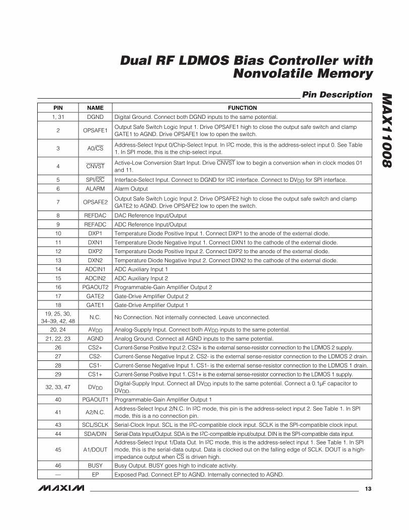
Pin DescriptionPIN NAME FUNCTION
1, 31 DGND Digital Ground. Connect both DGND inputs to the same potential.
2 OPSAFE1Output Safe Switch Logic Input 1. Drive OPSAFE1 high to close the output safe switch and clampGATE1 to AGND. Drive OPSAFE1 low to open the switch.
3 A0/CSAddress-Select Input 0/Chip-Select Input. In I2C mode, this is the address-select input 0. See Table1. In SPI mode, this is the chip-select input.
4 CNVSTActive-Low Conversion Start Input. Drive CNVST low to begin a conversion when in clock modes 01and 11.
5 SPI/I2C Interface-Select Input. Connect to DGND for I2C interface. Connect to DVDD for SPI interface.
6 ALARM Alarm Output
7 OPSAFE2Output Safe Switch Logic Input 2. Drive OPSAFE2 high to close the output safe switch and clampGATE2 to AGND. Drive OPSAFE2 low to open the switch.
8 REFDAC DAC Reference Input/Output
9 REFADC ADC Reference Input/Output
10 DXP1 Temperature Diode Positive Input 1. Connect DXP1 to the anode of the external diode.
11 DXN1 Temperature Diode Negative Input 1. Connect DXN1 to the cathode of the external diode.
12 DXP2 Temperature Diode Positive Input 2. Connect DXP2 to the anode of the external diode.
13 DXN2 Temperature Diode Negative Input 2. Connect DXN2 to the cathode of the external diode.
14 ADCIN1 ADC Auxiliary Input 1
15 ADCIN2 ADC Auxiliary Input 2
16 PGAOUT2 Programmable-Gain Amplifier Output 2
17 GATE2 Gate-Drive Amplifier Output 2
18 GATE1 Gate-Drive Amplifier Output 1
19, 25, 30,34–39, 42, 48
N.C. No Connection. Not internally connected. Leave unconnected.
20, 24 AVDD Analog-Supply Input. Connect both AVDD inputs to the same potential.
21, 22, 23 AGND Analog Ground. Connect all AGND inputs to the same potential.
26 CS2+ C ur r ent- S ense P osi ti ve Inp ut 2. C S 2+ i s the exter nal sense- r esi stor connecti on to the LD M OS 2 sup p l y.
27 CS2- Current-Sense Negative Input 2. CS2- is the external sense-resistor connection to the LDMOS 2 drain.
28 CS1- Current-Sense Negative Input 1. CS1- is the external sense-resistor connection to the LDMOS 1 drain.
29 CS1+ C ur r ent- S ense P osi ti ve Inp ut 1. C S 1+ i s the exter nal sense- r esi stor connecti on to the LD M OS 1 sup p l y.
32, 33, 47 DVDDDigital-Supply Input. Connect all DVDD inputs to the same potential. Connect a 0.1µF capacitor toDVDD.
40 PGAOUT1 Programmable-Gain Amplifier Output 1
41 A2/N.C.Address-Select Input 2/N.C. In I2C mode, this pin is the address-select input 2. See Table 1. In SPImode, this is a no connection pin.
43 SCL/SCLK Serial-Clock Input. SCL is the I2C-compatible clock input. SCLK is the SPI-compatible clock input.
44 SDA/DIN S er i al - D ata Inp ut/Outp ut. S D A i s the I2C- com p ati b l e i np ut/outp ut. D IN i s the S P I- com p ati b l e d ata i np ut.
45 A1/DOUTAddress-Select Input 1/Data Out. In I2C mode, this is the address-select input 1. See Table 1. In SPImode, this is the serial-data output. Data is clocked out on the falling edge of SCLK. DOUT is a high-impedance output when CS is driven high.
46 BUSY Busy Output. BUSY goes high to indicate activity.
— EP Exposed Pad. Connect EP to AGND. Internally connected to AGND.

MA
X1
10
08
Dual RF LDMOS Bias Controller withNonvolatile Memory
14 ______________________________________________________________________________________14 ______________________________________________________________________________________
MAX11008
PGAOUT2
REGISTER MAPAND DIGITAL
CONTROL
SERIAL INTERFACE
FIFO
EEPROM
PGA 1
12-BIT DAC 2
PGA 2
12-BIT ADC
2.5VREFERENCE
INTERNALTEMPERATURE
SENSOR
EXTERNALTEMPERATURE
SENSORPROCESSING
12-BIT DAC1
AV = 2
AV = 2
MUX
SCL/SCLK
SDA/DIN
A0/CS
DXP1
DXN1
DXP2
DXN2
ADCIN1
ADCIN2
PGAOUT1
CS1-
CS1+
CS2+
CS2-
GATE1
GATE2
OPSAFE1
OPSAFE2
REFDAC
REFADC
AGNDDGND
DVDD AVDD
CNVST
ALARM
BUSY
A1/DOUTA2/N.C.
SPI/I2C
Functional Diagram
MA
X1
10
08
Dual RF LDMOS Bias Controller withNonvolatile Memory
______________________________________________________________________________________ 15______________________________________________________________________________________ 15
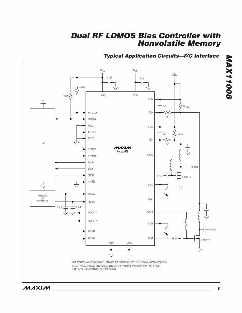
32V
RF OUT
RF IN
LDMOS 2
LDMOS 1
RF OUT
RF IN
CF*
CF*
RF*
RF*
RSENSE
RSENSE
0.1µF
4.7kΩ
4.7kΩ
0.1µF
DVDD AVDD
µC
5V
EXTERNAL2.5V
REFERENCE
0.1µF 0.1µF
MAX11008
OPSAFE2
OPSAFE1
SCL/SCLK
SDA/DIN
ALARM
BUSY
PGAOUT1
PGAOUT2
REFADC
REFDAC
ADCIN1
ADCIN2
CNVST
A0/CS
A1/DOUT
A2/N.C.
SPI/I2C
DGND AGND
CS1+
CS1-
GATE1
CS2+
CS2-
GATE2
DXP2
DXN2
DXP1
DXN1
DVDD AVDD
*SELECT RF AND CF BASED ON DESIRED FILTER CUTOFF FREQUENCY WHERE fCUTOFF = 1/(2 π RFCF). *SDA RESISTOR VALUE VARIES WITH LOAD AND SCL FREQUENCY. SEE THE I2C SERIAL INTERFACE SECTION.
LIMIT RF TO 100Ω TO MINIMIZE OFFSET ERRORS.
Typical Application Circuits—I2C Interface
MA
X1
10
08
Dual RF LDMOS Bias Controller withNonvolatile Memory
16 ______________________________________________________________________________________
µC
5V
EXTERNAL2.5V
REFERENCE
0.1µF 0.1µF
DVDD
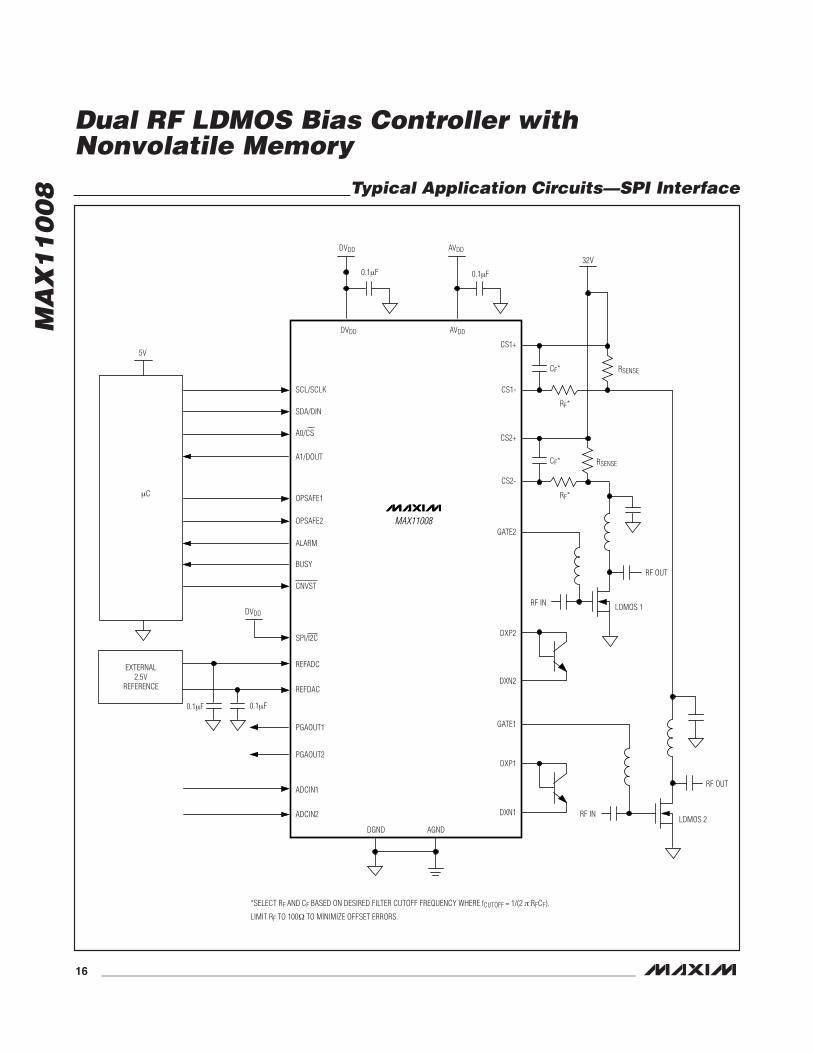
*SELECT RF AND CF BASED ON DESIRED FILTER CUTOFF FREQUENCY WHERE fCUTOFF = 1/(2 π RFCF).
LIMIT RF TO 100Ω TO MINIMIZE OFFSET ERRORS.
32V
RF OUT
RF IN
LDMOS 2
LDMOS 1
RF OUT
RF IN
CF*
CF*
RF*
RF*
RSENSE
RSENSE
0.1µF 0.1µF
DVDD AVDD
MAX11008
DGND AGND
CS1+
CS1-
GATE1
CS2+
CS2-
GATE2
DXP2
DXN2
DXP1
DXN1
DVDD AVDD
OPSAFE2
OPSAFE1
SCL/SCLK
SDA/DIN
ALARM
BUSY
PGAOUT1
REFADC
REFDAC
ADCIN1
ADCIN2
CNVST
A0/CS
A1/DOUT
SPI/I2C
PGAOUT2
Typical Application Circuits—SPI Interface
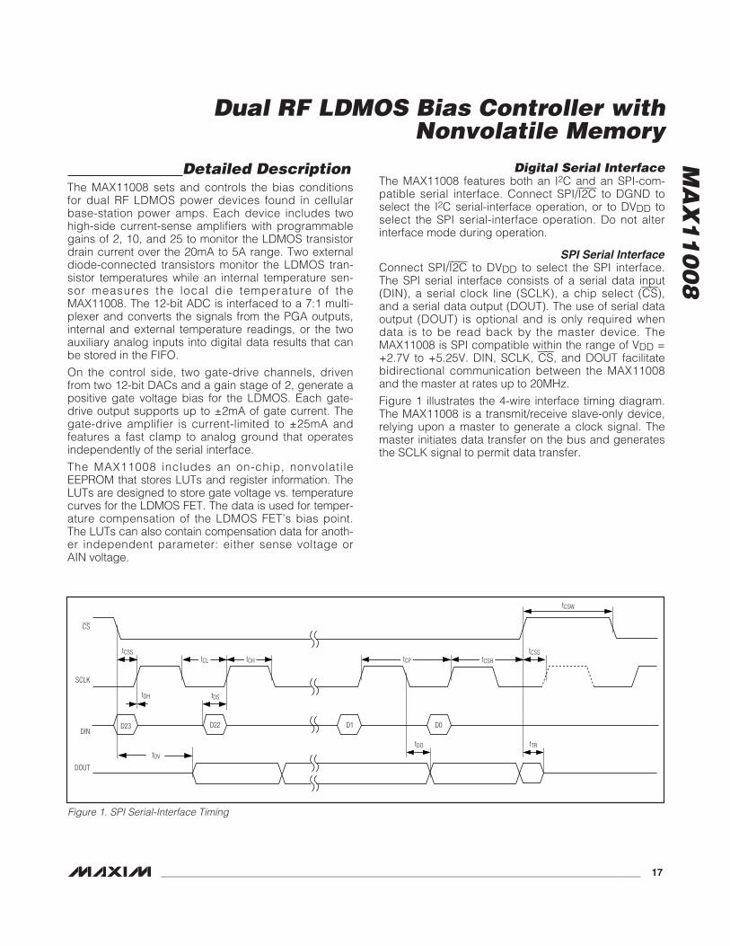
Detailed DescriptionThe MAX11008 sets and controls the bias conditionsfor dual RF LDMOS power devices found in cellularbase-station power amps. Each device includes twohigh-side current-sense amplifiers with programmablegains of 2, 10, and 25 to monitor the LDMOS transistordrain current over the 20mA to 5A range. Two externaldiode-connected transistors monitor the LDMOS tran-sistor temperatures while an internal temperature sen-sor measures the local die temperature of theMAX11008. The 12-bit ADC is interfaced to a 7:1 multi-plexer and converts the signals from the PGA outputs,internal and external temperature readings, or the twoauxiliary analog inputs into digital data results that canbe stored in the FIFO.
On the control side, two gate-drive channels, drivenfrom two 12-bit DACs and a gain stage of 2, generate apositive gate voltage bias for the LDMOS. Each gate-drive output supports up to ±2mA of gate current. Thegate-drive amplifier is current-limited to ±25mA andfeatures a fast clamp to analog ground that operatesindependently of the serial interface.
The MAX11008 includes an on-chip, nonvolatileEEPROM that stores LUTs and register information. TheLUTs are designed to store gate voltage vs. temperaturecurves for the LDMOS FET. The data is used for temper-ature compensation of the LDMOS FET’s bias point.The LUTs can also contain compensation data for anoth-er independent parameter: either sense voltage orAIN voltage.
Digital Serial InterfaceThe MAX11008 features both an I2C and an SPI-com-patible serial interface. Connect SPI/I2C to DGND toselect the I2C serial-interface operation, or to DVDD toselect the SPI serial-interface operation. Do not alterinterface mode during operation.
SPI Serial InterfaceConnect SPI/I2C to DVDD to select the SPI interface.The SPI serial interface consists of a serial data input(DIN), a serial clock line (SCLK), a chip select (CS),and a serial data output (DOUT). The use of serial dataoutput (DOUT) is optional and is only required whendata is to be read back by the master device. TheMAX11008 is SPI compatible within the range of VDD =+2.7V to +5.25V. DIN, SCLK, CS, and DOUT facilitatebidirectional communication between the MAX11008and the master at rates up to 20MHz.
Figure 1 illustrates the 4-wire interface timing diagram.The MAX11008 is a transmit/receive slave-only device,relying upon a master to generate a clock signal. Themaster initiates data transfer on the bus and generatesthe SCLK signal to permit data transfer.
MA
X1
10
08
Dual RF LDMOS Bias Controller withNonvolatile Memory
______________________________________________________________________________________ 17
tCSS
SCLK
tDH
tDV
tDS
CS
DIN
DOUT
D23 D22 D1 D0
tCH tCSH
tCSS
tCSW
tCL tCP
tDO tTR
Figure 1. SPI Serial-Interface Timing

MA
X1
10
08 The SPI bus cycles are 24 bits long. Data can be sup-
plied as three 8-bit bytes or as a continuous 24-bitstream. CS must remain low throughout the 24-bitsequence. The first 8-bit byte is a command byteC[7:0]. The next 16 bits are data bits D[15:0]. Clocksignal SCLK can idle low or high, but data is alwaysclocked in on the rising edge of SCLK (CPOL = CPHA).
SPI data transfers begin with the falling edge of CS.Data is clocked into the device on the rising edges ofSCLK and clocked out of the device on the fallingedges of SCLK. For correct bus cycles, CS shouldframe the data and should not return to a 1 until afterthe last active rising clock edge. See Figure 2 for timingdetails. A rising edge of CS causes DOUT to three-state and data reads should be performed accordingly.See Figures 1 and 3.
When writing instructions to the MAX11008, 24 clockcycles must be completed before CS is driven high.The MAX11008 executes the instruction only after the24th clock cycle has been received and CS is drivenhigh. To abort unwanted instructions, CS can be drivenhigh at any time before the 23rd rising clock edge.
When reading data from the MAX11008, 24 clockcycles must be completed before CS is driven high. IfCS is driven high before the completion of the 24thfalling edge, DOUT immediately three-states, the inter-face resets in preparation for the next command, andthe data being read is lost.
Write FormatUse the following sequence to write 16 bits of data to aMAX11008 register (see Figure 2):
1) Drive CS low to select the device.
2) Send the appropriate write command byte (seeTable 6 for the register address map). The com-mand byte is clocked in on the rising edge of SCLK.
3) Send 16 bits of data D[15:0] starting with the mostsignificant bit (MSB). Data is clocked in on the risingedges of SCLK.
4) Drive CS high to conclude the command.
Dual RF LDMOS Bias Controller withNonvolatile Memory
18 ______________________________________________________________________________________
SCLK
C6CR/W- C4C5 C2C3 C0C1DIN D15 D14 D13 D12 D11 D10 D9 D8 D7 D6 D5 D4 D3 D2 D1 D0
CS
A RISING EDGE OF CSDURING THIS PERIOD
COMPLETES A VALID WRITECOMMAND
Figure 2. SPI Write Sequence

Read FormatUse the following sequence to read 16 bits of data froma MAX11008 register (see Figure 3):
1) Drive CS low to select the device.
2) Send the appropriate read command byte (seeTable 6 for the register address map). The com-mand byte is clocked in on the rising edges ofSCLK.
3) Receive 16 bits of data. The first 4 bits of data arealways high. Data is clocked out on the falling edgesof SCLK.
4) Drive CS high.
I2C Serial InterfaceConnect SPI/I2C to DGND to select the I2C interface. TheI2C serial interface consists of a serial data line (SDA)and a serial clock line (SCL). The MAX11008 is I2C com-patible within the DVDD = 2.7V to 5.25V range. SDA andSCL facilitate bidirectional communication between theMAX11008 and the master at rates up to 400kHz for fastmode and up to 3.4MHz for high-speed mode (HSmode). See the Bus Timing and HS I2C Mode sectionsfor more information on data-rate configurations.
Figure 4 shows the 2-wire interface timing diagram. TheMAX11008 is a transmit/receive slave-only device, rely-ing upon a master to generate a clock signal. The mas-ter (typically a microcontroller) initiates data transferson the bus and generates the SCL signal to permit datatransfer.
MA
X1
10
08
Dual RF LDMOS Bias Controller withNonvolatile Memory
______________________________________________________________________________________ 19
SCLK
C6R/W C4C5 C2C3 C0C1DIN
CS
DOUT D14 D13 D12 D11 D10 D9 D8 D6 D5 D4 D3 D2 D1D15 D7 D0
X X X X X X X X X X X X X X X X X X
Figure 3. SPI Read Sequence
SDA
SCL
tSU, DAT
tHD, STA
tHD, STAtRCL
tLOW
tHIGH
tR tF
tHIGH
tRCL
tLOW
tSU, DAT tHD, DAT
tHD, DAT tHD, STA
tR tF
tBUF
tBUF
tRDA tRDA
tRCL
tHD, STA
tSU, STA tSU, ST0
tSU, ST0tSU, STA
SCL
S Sr A
Sr A P S
P
F/S MODEHS MODE
S
S
SDA
a) F/S-MODE I2C SERIAL INTERFACE TIMING
b) HS-MODE I2C SERIAL INTERFACE TIMING
PARAMETERS ARE MEASURED FROM 30% TO 70%.
Figure 4. I2C Serial-Interface Timing Diagram

MA
X1
10
08 A master device communicates to the MAX11008 by
transmitting the proper slave address followed by acommand and/or data words. Each transmit sequenceis framed by a START (S) or repeated START (Sr) con-dition and a STOP (P) condition. Each word transmittedover the bus is 8 bits long and is always followed by anacknowledge clock pulse.
The MAX11008 SDA and SCL drivers are open-drainoutputs, requiring a pullup resistor (750Ω or greater) togenerate a logic-high voltage (see the TypicalApplication Circuits). Series resistors are optional fornoise filtering. These series resistors protect the inputstages of the MAX11008 from high-voltage spikes onthe bus line, and minimize crosstalk and undershoot ofthe bus signals.
Bit TransferOne data bit is transferred during each SCL clockcycle. The data on SDA must remain stable during thehigh period of the SCL clock pulse. Changes in SDAwhile SCL is high are control signals (see the STARTand STOP Conditions section). Both SDA and SCL idlehigh when the I2C bus is not busy.
START and STOP ConditionsThe master initiates a transmission with a START condi-tion (S), which is a high-to-low transition on SDA while
SCL is high. The master terminates a transmission witha STOP condition (P), which is a low-to-high transitionon SDA while SCL is high (see Figure 5). A repeatedSTART condition (Sr) can be used in place of a STOPcondition to leave the bus active and the modeunchanged (see the HS I2C Mode section).
Acknowledge Bits and Not-Acknowledge ConditionsData transfers are framed with an acknowledge bit(ACK) or a not-acknowledge bit (NACK). Both the mas-ter and the MAX11008 (slave) generate acknowledgebits. To generate an acknowledge, the receiving devicemust pull SDA low before the rising edge of theacknowledge-related clock pulse (ninth clock pulse)and keep it low during the high period of the clockpulse (see Figure 6).
To generate a not-acknowledge condition, the receiverallows SDA to be pulled high before the rising edge ofthe acknowledge-related clock pulse, and leaves SDAhigh during the high period of the clock pulse.Monitoring the acknowledge bits allows for detection ofunsuccessful data transfers. An unsuccessful datatransfer happens if a receiving device is busy or if asystem fault has occurred. In the event of an unsuc-cessful data transfer, the bus master reattempts com-munication at a later time.
Dual RF LDMOS Bias Controller withNonvolatile Memory
20 ______________________________________________________________________________________
SDA
S Sr P
SCL
S = START.Sr = REPEATED START.P = STOP.
Figure 5. START and STOP Conditions
SDA
S
1 2 8
NOT ACKNOWLEDGE
ACKNOWLEDGE
9SCL
Figure 6. Acknowledge Bits
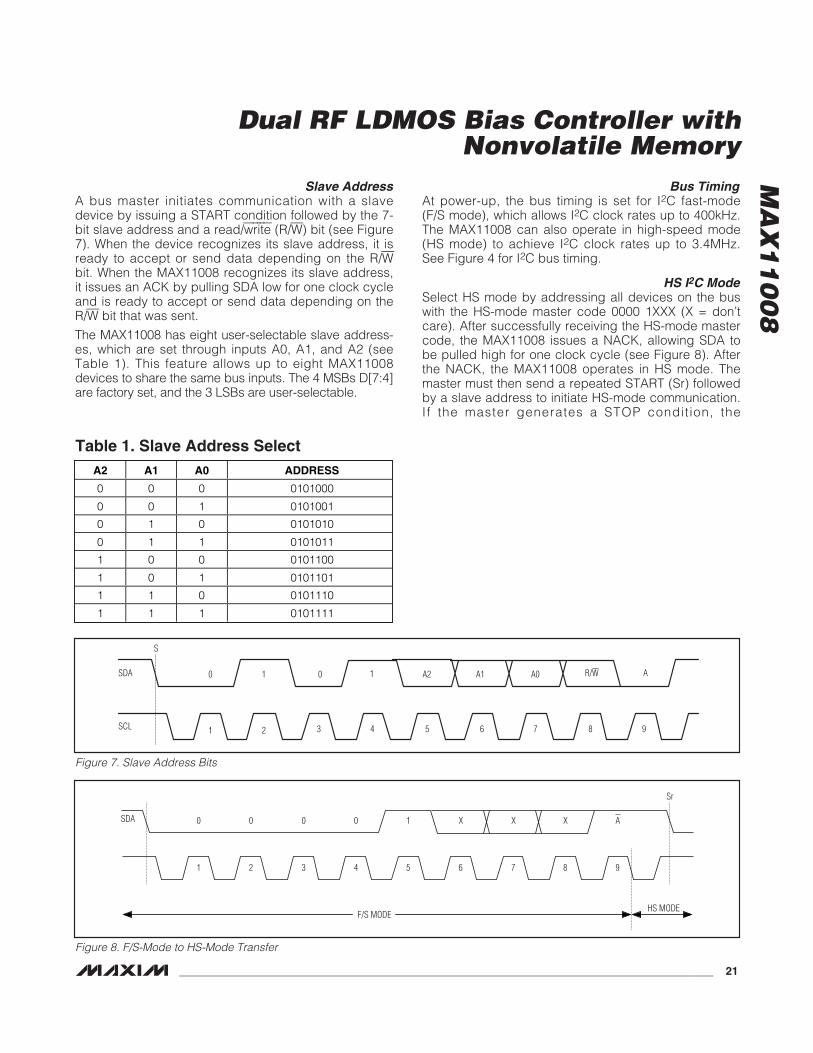
Slave AddressA bus master initiates communication with a slavedevice by issuing a START condition followed by the 7-bit slave address and a read/write (R/W) bit (see Figure7). When the device recognizes its slave address, it isready to accept or send data depending on the R/Wbit. When the MAX11008 recognizes its slave address,it issues an ACK by pulling SDA low for one clock cycleand is ready to accept or send data depending on theR/W bit that was sent.
The MAX11008 has eight user-selectable slave address-es, which are set through inputs A0, A1, and A2 (seeTable 1). This feature allows up to eight MAX11008devices to share the same bus inputs. The 4 MSBs D[7:4]are factory set, and the 3 LSBs are user-selectable.
Bus TimingAt power-up, the bus timing is set for I2C fast-mode(F/S mode), which allows I2C clock rates up to 400kHz.The MAX11008 can also operate in high-speed mode(HS mode) to achieve I2C clock rates up to 3.4MHz.See Figure 4 for I2C bus timing.
HS I2C ModeSelect HS mode by addressing all devices on the buswith the HS-mode master code 0000 1XXX (X = don’tcare). After successfully receiving the HS-mode mastercode, the MAX11008 issues a NACK, allowing SDA tobe pulled high for one clock cycle (see Figure 8). Afterthe NACK, the MAX11008 operates in HS mode. Themaster must then send a repeated START (Sr) followedby a slave address to initiate HS-mode communication.If the master generates a STOP condition, the
MA
X1
10
08
Dual RF LDMOS Bias Controller withNonvolatile Memory
______________________________________________________________________________________ 21
SDA
SCL
0 0 A2 A1 A0 R/W A
1 2 3 4 5 6 7 8 9
S
1 1
Figure 7. Slave Address Bits
SDA
1 2 3 4
0 0 0 0
5 6 7 8
1 X X X
9
A
Sr
HS MODEF/S MODE
Figure 8. F/S-Mode to HS-Mode Transfer
A2 A1 A0 ADDRESS
0 0 0 0101000
0 0 1 0101001
0 1 0 0101010
0 1 1 0101011
1 0 0 0101100
1 0 1 0101101
1 1 0 0101110
1 1 1 0101111
Table 1. Slave Address Select
MA
X1
10
08 MAX11008 returns to F/S mode. Use a repeated START
condition in place of a STOP condition to leave the busactive and the mode unchanged. Figure 9 summarizesthe data bit transfer format for HS-mode communication.
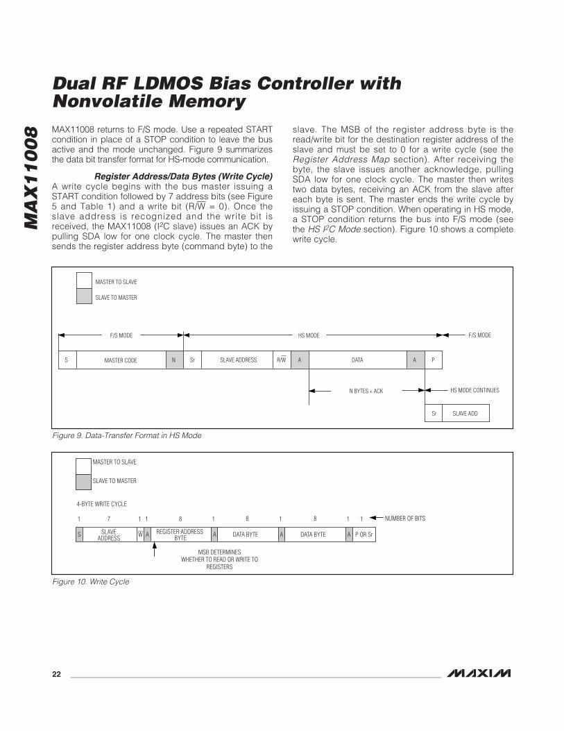
Register Address/Data Bytes (Write Cycle)A write cycle begins with the bus master issuing aSTART condition followed by 7 address bits (see Figure5 and Table 1) and a write bit (R/W = 0). Once theslave address is recognized and the write bit isreceived, the MAX11008 (I2C slave) issues an ACK bypulling SDA low for one clock cycle. The master thensends the register address byte (command byte) to the
slave. The MSB of the register address byte is theread/write bit for the destination register address of theslave and must be set to 0 for a write cycle (see theRegister Address Map section). After receiving thebyte, the slave issues another acknowledge, pullingSDA low for one clock cycle. The master then writestwo data bytes, receiving an ACK from the slave aftereach byte is sent. The master ends the write cycle byissuing a STOP condition. When operating in HS mode,a STOP condition returns the bus into F/S mode (seethe HS I2C Mode section). Figure 10 shows a completewrite cycle.
Dual RF LDMOS Bias Controller withNonvolatile Memory
22 ______________________________________________________________________________________
S MASTER CODE N Sr SLAVE ADDRESS R/W A DATA A P
Sr SLAVE ADD
F/S MODE HS MODE
N BYTES + ACK HS MODE CONTINUES
F/S MODE
MASTER TO SLAVE
SLAVE TO MASTER
Figure 9. Data-Transfer Format in HS Mode
SLAVE TO MASTER
MASTER TO SLAVE
S
1
SLAVEADDRESS A
7 1 1
W REGISTER ADDRESS BYTE
8
P OR Sr
1
MSB DETERMINESWHETHER TO READ OR WRITE TO
REGISTERS
4-BYTE WRITE CYCLE
NUMBER OF BITS
A
1
DATA BYTE
8
A
1
DATA BYTE
8
A
1
Figure 10. Write Cycle

Register Address/Data Bytes (5-Byte Read Cycle)A read cycle begins with the master issuing a STARTcondition followed by a 7-bit address, (see Figure 5and Table 1) and a write bit (R/W = 0) to instruct theMAX11008 interface that it is about to receive data.Once the slave address is recognized and the write bitis received, the MAX11008 (I2C slave) issues an ACKby pulling SDA low for one clock cycle. The masterthen sends the register address byte (command byte)to the slave. The MSB of the register address byte isthe read/write bit for the destination register address ofthe slave and must be set to 1 for a read cycle (see theRegister Address Map section). After this byte isreceived, another acknowledge bit is sent to the masterfrom the slave. The master then issues a repeatedSTART (Sr) condition. Following a repeated START (Sr),the master writes the slave address byte again with aread bit (R/W = 1). After a third acknowledge signalfrom the slave, the data direction on the SDA busreverses and the slave writes the 2 data bytes (the
contents of the register that was addressed in the pre-vious command byte) to the master. Finally, the masterissues a NACK followed by a STOP condition (P), end-ing the read cycle. Figure 11 shows a complete 5-byteread cycle.
Default Read Cycle (3-Byte Read Cycle)The MAX11008 2-wire interface has a unique feature forread commands. To avoid the necessity of sending 2slave address bytes in one read cycle (see the 5-byteread cycle in Figure 11), the MAX11008 2-wire interfacerecognizes a single slave address byte with a read bit(R/W = 1). In this case, the interface outputs the con-tents of the last read device register. This default readfeature is useful when the master must perform multipleconsecutive reads from the same device register.Figure 11 shows a complete 3-byte read cycle.
MA
X1
10
08
Dual RF LDMOS Bias Controller withNonvolatile Memory
______________________________________________________________________________________ 23
S
1
SLAVEADDRESS
SLAVEADDRESS
SLAVEADDRESS
A
7 1 1
W COMMAND BYTE
8
P OR Sr
P OR Sr
1
5-BYTE READ CYCLE
NUMBER OF BITS
NUMBER OF BITS
A Sr
1
DATA BYTE
8 1
DATA BYTE
8 1
A A
7 1 1
R
7 1
RS
1
3-BYTE READ CYCLE
1
DATA BYTE DATA BYTE
8
A
1 8
N
N
1
A
1
SLAVE TO MASTER
MASTER TO SLAVE
Figure 11. 5-Byte and 3-Byte Read Cycle

MA
X1
10
08 12-Bit ADC
The MAX11008 12-bit ADC uses a SAR conversiontechnique and on-chip track-and-hold (T/H) circuitry toconvert the PGA outputs (PGAOUT1 and PGAOUT2),temperature measurements, and single-ended auxiliaryinput voltages (ADCIN1 and ADCIN2) into 12-bit digitaldata when in ADC monitor mode (see the HardwareConfiguration Register (HCFIG) (Read/Write) section).All nontemperature measurements are converted usinga unipolar transfer function (see Figure 13), and all tem-perature measurements are converted using a bipolartransfer function (see Figure 14).
Analog Input T/HFigure 12 shows the equivalent circuit for the ADC inputarchitecture of the MAX11008. In track mode, an inputcapacitor is connected to the input signal (ADCIN1,ADCIN2, PGAOUT1, PGAOUT2, or temperature sensorprocessor output). Another input capacitor is connect-ed to AGND. After the T/H enters hold mode, the differ-ence between the sampled positive and negative inputvoltages is converted. The charging rate of the inputcapacitance determines the time required for the T/H toacquire an input signal. If the input signal’s sourceimpedance is high, the required acquisition timelengthens accordingly.
Any source impedance below 300Ω does not affect theADC’s AC performance. A high-impedance source canbe accommodated either by lengthening tACQ or byplacing a 1µF capacitor between the positive and neg-ative analog inputs. The combination of the analog-input source impedance and the capacitance at theanalog input creates an RC filter that limits the analoginput bandwidth.
Input BandwidthThe ADC’s input-tracking circuitry has a 1MHz small-signal bandwidth, to digitize high-speed transientevents and measure periodic signals with bandwidthsexceeding the ADC’s sampling rate by using under-sampling techniques. Anti-alias filtering of the input sig-nals is necessary to prevent high-frequencycomponents from aliasing into the frequency band ofinterest.
Analog Input ProtectionInternal electrostatic-discharge (ESD) protection diodesclamp all analog inputs to AVDD and AGND, allowingthe inputs to swing from (AGND - 0.3V) to (AVDD +0.3V) without damage. However, for accurate conver-sions near full scale, the inputs must not exceed AVDDby more than 50mV or be lower than AGND by 50mV. Ifan analog input voltage exceeds the supplies, limit theinput current to 2mA.
Dual RF LDMOS Bias Controller withNonvolatile Memory
24 ______________________________________________________________________________________
HOLD
HOLD HOLD
CAPACITIVEDAC
REFADC
CIN+
CIN-
TRACK
AGND
ADCIN1ADCIN2
PGAOUT1PGAOUT2
TEMP SENSOR READING
TRACK
TRACK
ALL SWITCHES SHOWN IN TRACK MODE.
COMPARATOR
AVDD/2
Figure 12. Analog Input Track and Hold

ADC Transfer FunctionsFigure 13 shows the unipolar transfer function for non-temperature measurements, and Figure 14 shows thebipolar transfer function used for temperature measure-ments. Code transitions occur halfway between suc-cessive-integer LSB values. Output coding is binary,with 1 LSB = VREFADC/4096 for nontemperature mea-surements, and 1 LSB = +0.125°C for temperaturemeasurements. All signed binary results use two’s com-plement format.
ADC Conversion SchedulingThe MAX11008 ADC multiplexer scans and convertsthe selected inputs in the order shown in Table 2 (seethe ADC Conversion Register (ADCCON) (Write Only)section) when more than one channel is selected. Theresults are stored in the FIFO when in ADC monitoringmode. The BUSY signal is set at the start and reset atthe end of a scan except when the continuous convertbit is set at which time BUSY does not then respond toADC conversions.
Writing a conversion command before a conversion iscomplete cancels the pending conversion. Avoidaddressing the device using the serial interface whilethe ADC is converting.
ADC Clock ModesThe MAX11008 offers three conversion/acquisitionmodes (known as clock modes) selectable throughconfiguration register bits CKSEL1 and CKSEL0.
If the ADC conversion requires the internal reference(temperature measurement or voltage measurement withinternal reference selected) and the reference has notbeen previously forced on (FBGON = 1), the deviceinserts a typical delay of 72µs, for the reference to settle,before commencing the ADC conversion. The referenceremains powered up while there are pending conver-sions. If the reference is not forced on, it automaticallypowers down at the end of a scan or when CONCONV inthe ADC Conversion register is set back to 0.
Internally Timed Acquisitionsand Conversions
Clock Mode 00In clock mode 00, power-up, acquisition, conversion,and power-down are all initiated by writing to the ADCConversion register and performed automatically usingthe internal oscillator. This is the default clock mode.The ADC sets the BUSY output high, powers up, andscans all requested channels storing the results in theFIFO if the ADCMON bit has been set. After the scan is
MA
X1
10
08
Dual RF LDMOS Bias Controller withNonvolatile Memory
______________________________________________________________________________________ 25
FULL-SCALE TRANSITION
INPUT VOLTAGE (LSB)
BINA
RY O
UTPU
T CO
DE
0
0000 0000 0001
0000 0000 0000
0000 0000 0010
0000 0000 0011
1111 1111 1101
1111 1111 1100
1111 1111 1110
1111 1111 1111
1 LSB = VREFADC/4096
1 2 3 4093 4095
VREFADC
V REF
ADC
Figure 13. ADC Transfer Function
TEMPERATURE (°C)
OUTP
UT C
ODE
-256 +25501000 0000 0000
1000 0000 0001
0000 0000 0001
0111 1111 1111
0111 1111 1110
0111 1111 1101
0000 0000 0000
1111 1111 1111
1000 0000 0010
1 LSB = +0.125°C
Figure 14. Temperature Transfer Function
ORDER OF SCAN DESCRIPTION OF CONVERSION
1 Internal device temperature
2 External diode 1 temperature
3 Output of PGA 1 for current sense
4 Auxiliary input 1 (ADCIN1)
5 External diode 2 temperature
6 Output of PGA 2 for current sense
7 Auxiliary input 2 (ADCIN2)
Table 2. Order of ADC Conversion Scan

MA
X1
10
08 complete the ADC powers down, BUSY is pulled low,
and the results for all of the selected channels areavailable in the FIFO.
The duration of the BUSY pulse is additive, dependingon the channel conversion sequence selected. TheBUSY pulse is set typically for 72µs by temperatureconversions; 52µs by PGAOUT conversions, and 7µsby ADCIN conversions.
Clock Mode 01In clock mode 01, power-up, acquisition, conversion,and power-down are all initiated through a single pulseon CNVST and performed automatically using the inter-nal oscillator. Initiate a scan by writing to the ADC con-version register and setting CNVST low for at least20ns. The ADC sets the BUSY output high, powers up,and scans all requested channels storing the results inthe FIFO if the ADCMON bit has been set. After thescan is complete, the ADC powers down, BUSY ispulled low, and the results for all of the selected chan-nels are available in the FIFO. The BUSY pulse behav-ior is identical to that of clock mode 00.
Externally TimedAcquisitions and Conversions
Clock Mode 10Clock mode 10 is reserved. Do not use this clockmode.
Clock Mode 11In clock mode 11, set the FBGON bit. Conversions areinitiated one at a time through CNVST and performedusing the internal oscillator. In this mode, the acquisitiontime is controlled by the time CNVST is low. CNVST isresynchronized by the internal oscillator, resulting in aone-clock cycle (typically 320ns) uncertainty in the exactsampling instant. Different timing parameters applydepending if the conversion is temperature, from ADCIN,or from PGAOUT (as specified in the Clock Mode 00section). Figure 15 shows a conversion time example.
Both internal and external temperature conversions areinternally timed. Pull CNVST low for a minimum of 20ns(tCNV11) to trigger a temperature conversion. The BUSYoutput goes high and the temperature conversion resultis available in the FIFO (if the ADCMON bit is set) 72µs(typ) after BUSY goes low again.
Dual RF LDMOS Bias Controller withNonvolatile Memory
26 ______________________________________________________________________________________
BUSY
CNVST
INTERNALOPERATIONS
TEMPERATURECONVERSION
70µs (typ)
INTERNAL TEMPERATURE READING, PGA1 OUTPUT, AND ADCIN1 CONVERSION TIMING IN CLOCK MODE 11
tCNV = 20ns (typ)tACQ = 30µs (typ)
tACQ = 1.5µs (typ)
WRITE TO ADCCONVERT REGISTER TO
SET UP ADC SCANFBGON = 1,
ADCMON = 1
TEMPERATURECONVERSION RESULT
AVAILABLE IN FIFO
IDLE MODE,REF AND
TEMPSENSOR
POWERED
PGA 1ACQUISITION
END OFSCAN
PGA 1CONVERSION
22µs (typ)
IDLE MODE,REF AND
TEMPSENSOR
POWERED
ADCI
N1AC
QUIS
ITIO
NAD
CIN1
CONV
ERSI
ON7µ
s (typ
)
PGA 1 OUTPUTCONVERSION
RESULT AVAILABLEIN FIFO
ADCIN 1CONVERSION
RESULT AVAILABLEIN FIFO
Figure 15. ADC Clock Mode 11 Example
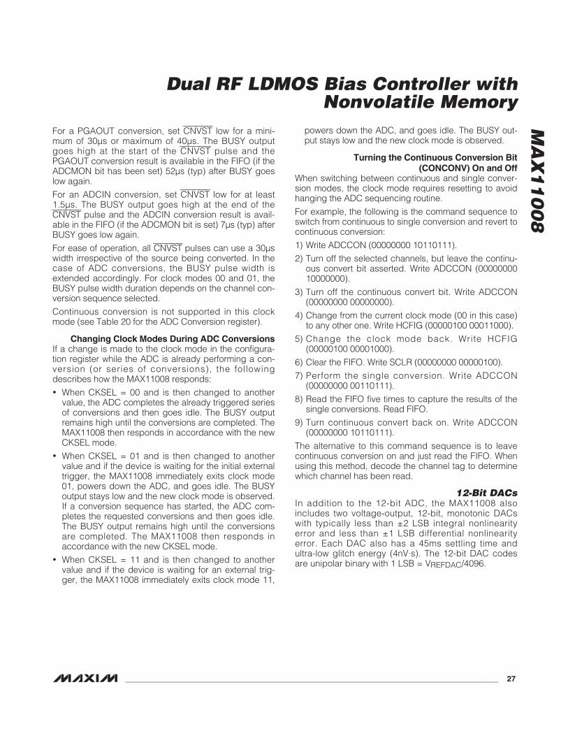
For a PGAOUT conversion, set CNVST low for a mini-mum of 30µs or maximum of 40µs. The BUSY outputgoes high at the start of the CNVST pulse and thePGAOUT conversion result is available in the FIFO (if theADCMON bit has been set) 52µs (typ) after BUSY goeslow again.
For an ADCIN conversion, set CNVST low for at least1.5µs. The BUSY output goes high at the end of theCNVST pulse and the ADCIN conversion result is avail-able in the FIFO (if the ADCMON bit is set) 7µs (typ) afterBUSY goes low again.
For ease of operation, all CNVST pulses can use a 30µswidth irrespective of the source being converted. In thecase of ADC conversions, the BUSY pulse width isextended accordingly. For clock modes 00 and 01, theBUSY pulse width duration depends on the channel con-version sequence selected.
Continuous conversion is not supported in this clockmode (see Table 20 for the ADC Conversion register).
Changing Clock Modes During ADC ConversionsIf a change is made to the clock mode in the configura-tion register while the ADC is already performing a con-version (or series of conversions), the followingdescribes how the MAX11008 responds:
• When CKSEL = 00 and is then changed to anothervalue, the ADC completes the already triggered seriesof conversions and then goes idle. The BUSY outputremains high until the conversions are completed. TheMAX11008 then responds in accordance with the newCKSEL mode.
• When CKSEL = 01 and is then changed to anothervalue and if the device is waiting for the initial externaltrigger, the MAX11008 immediately exits clock mode01, powers down the ADC, and goes idle. The BUSYoutput stays low and the new clock mode is observed.If a conversion sequence has started, the ADC com-pletes the requested conversions and then goes idle.The BUSY output remains high until the conversionsare completed. The MAX11008 then responds inaccordance with the new CKSEL mode.
• When CKSEL = 11 and is then changed to anothervalue and if the device is waiting for an external trig-ger, the MAX11008 immediately exits clock mode 11,
powers down the ADC, and goes idle. The BUSY out-put stays low and the new clock mode is observed.
Turning the Continuous Conversion Bit(CONCONV) On and Off
When switching between continuous and single conver-sion modes, the clock mode requires resetting to avoidhanging the ADC sequencing routine.
For example, the following is the command sequence toswitch from continuous to single conversion and revert tocontinuous conversion:
1) Write ADCCON (00000000 10110111).
2) Turn off the selected channels, but leave the continu-ous convert bit asserted. Write ADCCON (0000000010000000).
3) Turn off the continuous convert bit. Write ADCCON(00000000 00000000).
4) Change from the current clock mode (00 in this case)to any other one. Write HCFIG (00000100 00011000).
5) Change the clock mode back. Write HCFIG(00000100 00001000).
6) Clear the FIFO. Write SCLR (00000000 00000100).
7) Perform the single conversion. Write ADCCON(00000000 00110111).
8) Read the FIFO five times to capture the results of thesingle conversions. Read FIFO.
9) Turn continuous convert back on. Write ADCCON(00000000 10110111).
The alternative to this command sequence is to leavecontinuous conversion on and just read the FIFO. Whenusing this method, decode the channel tag to determinewhich channel has been read.
12-Bit DACsIn addition to the 12-bit ADC, the MAX11008 alsoincludes two voltage-output, 12-bit, monotonic DACswith typically less than ±2 LSB integral nonlinearityerror and less than ±1 LSB differential nonlinearityerror. Each DAC also has a 45ms settling time andultra-low glitch energy (4nV·s). The 12-bit DAC codesare unipolar binary with 1 LSB = VREFDAC/4096.
MA
X1
10
08
Dual RF LDMOS Bias Controller withNonvolatile Memory
______________________________________________________________________________________ 27

MA
X1
10
08 Figure 16 shows the functional diagram of the
MAX11008 DACs. Each DAC includes an input andoutput register. The input registers hold the result of themost recent write operation, and the output registershold the current output code for the respective DAC.Data written to a DAC input register is transferred to itsoutput register by writing to the Load DAC register (seeTable 22). Alternatively, write data directly to the outputregister using the DAC Input and Output Data register.
The analog output voltages of the DACs (before amplifi-cation by the gate-drive amplifiers) are calculated withthe following equation:
where VDACREF is the value of the internal or externalreference voltage and CODE is the decimal value of the12-bit code contained in the output register.
Gate-Drive AmplifiersThe gate-drive amplifiers are proportional to the analogoutputs of the 12-bit DACs and provide the necessarygate voltage to drive the external LDMOS transistors.Both amplifiers have a fixed gain of 2V/V and are capa-ble of sourcing or sinking up to 2mA of current. Outputshort-circuit protection prevents output currents fromexceeding ±25mA.
The gate output is equal to the DAC output voltageamplified by 2.
VGATE_ = 2 x VDAC
See the Software Configuration Registers andTemperature/APC LUT Configuration Registers sectionsfor information on how the gate voltages are controlledby temperature and APC samples.
Output ClampThe MAX11008 features an output clamp mode thatprotects the external LDMOS transistors by connectingthe gate-drive amplifier outputs (GATE_) to AGND. Theclamp mode can be controlled by the OPSAFE_ digitalinputs or by setting the appropriate ALMCLMP[1:0] bitsin the Alarm Hardware Configuration register (seeTable 14). When using the OPSAFE_ digital inputs, pullOPSAFE_ high to enter clamp mode and pull OPSAFE_low to exit clamp mode. The clamp can also be activat-ed automatically from the alarm trip point setting regis-ters; see the Alarm Software Configuration Register(ALMSCFIG) (Read/Write) section.
Self-CalibrationCalibrate channel 1 and channel 2 by writing to thePGA Calibration Control register. The MAX11008 func-tions after power-up without a calibration. Command acalibration after powering up the device by setting theTRACK bit to 0 and the DOCAL bit to 1 (see Table 19).Subsequently, set the TRACK, DOCAL, and SELFTIMEbits to 1 to enable automatic self-calibration (approxi-mately every 13ms). This minimizes loss of perfor-mance over temperature and supply-voltage variation.Alternatively, run self-calibration manually to control thetiming of the operation. Set the TRACK and DOCAL bitsto 1 and the SELFTIME bit to 0 to perform manually trig-gered self-calibration.
The self-calibration algorithm cancels offsets at thePGA-drive amplifier inputs in approximately 50µV incre-ments to improve accuracy. The self-calibration routinecan be commanded when the DACs are powereddown, but the results will not be accurate. For bestresults, run the calibration after the DAC power-up time,tDPUEXT. The ADC’s operation is suspended during aself-calibration. The BUSY output returning low indi-cates the end of the self-calibration routine. Wait untilthe end of the self-calibration routine before requestingan ADC conversion.
VV CODE
DACDACREF=
×
4096
Dual RF LDMOS Bias Controller withNonvolatile Memory
28 ______________________________________________________________________________________
Channel 1/Channel 2 CHANNEL 1/CHANNEL 2 DAC
CHANNEL 1/CHANNEL 2 DAC OUTPUT REGISTERS
CHANNEL 1/CHANNEL 2 DAC INPUT REGISTERS
LDDACCH_SET TO 1 INLOAD DACREGISTER
Figure 16. DAC Functional Diagram

ADC and DAC ReferencesThe MAX11008 provides an internal low-noise +2.5Vreference for the ADCs, DACs and temperature sensor.When using the internal reference the REFDAC andREFADC inputs can either be left open or to improvenoise performance, bypassed with a 0.1µF capacitor toAGND. Connect a voltage source to the REFADC inputranging between +1V to AVDD to configure the devicefor external ADC reference mode. Connect a voltagesource to the REFDAC input ranging between +0.7V to+2.5V to configure the device for external DAC refer-ence mode. When using an external voltage reference,bypass the REFDAC and REFADC inputs with a 0.1µFcapacitor to AGND. Bits D[3:0] within the HardwareConfiguration register control the source of the DACand ADC references. See Table 11.
Temperature SensorsThe MAX11008 measures the internal die temperatureand two external LDMOS transistor temperatures throughone internal and two external diode-connected transis-tors. The MAX11008 performs temperature measure-ments by changing the bias current of each diode from4µA to 68µA to produce a temperature-dependent biasvoltage difference. The internal ADC converts the volt-age difference to a digital value. The conversion result at4µA is subtracted from the conversion results at 68µA tocalculate a digital value that is proportional to absolutetemperature. The output data sent to the master will bethe resultant digital code minus an offset value to adjustfrom Kelvin to Celsius. Temperature data is delivered tothe master as a 12-bit signed (two’s complement) frac-tional number with the 3 LSBs being the fractional bits.This provides a temperature measurement resolution of1/8°C. See Table 3 for examples of the signed fractionalnumber digital temperature codes.
In clock mode 00, initiate temperature conversions bywriting 0x13 to the ADC Conversion register. In clockmode 01, initiate temperature conversions by writing0x13 to the ADC Conversion register and pulse CNVSTlow. In clock mode 11, initiate temperature conversionsby writing 0x13 to the ADC Conversion register andpulse CNVST low for each channel conversion. Set thecorresponding data bits for the temperature sensor tobe measured to 1 (see the ADC Conversion Register(ADCCON) (Write Only) section and Table 20) for allthree clock modes. Set the high and low external tem-perature thresholds through the temperature thresholdregisters. See the Low Temperature ThresholdRegisters (TL1, TL2) (Read/Write) section, HighTemperature Threshold Registers (TH1, TH2)(Read/Write) section, and Tables 7 and 8).
The reference voltage for the temperature measure-ments is always derived from the internal referencesource to ensure that 1 LSB corresponds to 1/8 of adegree Celsius. On every scan where only temperaturemeasurements are requested, temperature conversionsare carried out in the following order: INTEMP,EXTEMP1, then EXTEMP2. If the ADCMON bit is setwhen the conversions are performed, the temperaturereadings are available in the FIFO.
The temperature-sensing circuits power up at the startof an ADC conversion scan. The temperature-sensingcircuits remain powered on until the end of the scan toavoid a 50µs delay caused by the internal referencepower-up time required for each individual temperaturechannel. The temperature-sensor circuits remain pow-ered up when the ADC conversion register’s continu-ous convert bit (CONCONV, see Table 20) is set to 1and the current ADC conversion includes a tempera-ture channel. The temperature-sensor circuits remainpowered up until the CONCONV bit is set low.
The external temperature-sensor drive current ratio hasbeen optimized for a 2N3904 npn transistor with an ide-ality factor of 1.0065. The nonideality offset is removedinternally by a preset digital coefficient. Using a transis-tor with a different ideality factor produces a proportion-ate difference in the absolute measured temperature.For more details on this topic and others related tousing an external temperature sensor, refer toApplication Note 1057: Compensating for IdealityFactor and Series Resistance Differences betweenThermal Sense Diodes and Application Note 1944:Temperature Monitoring Using the MAX1253/54 andMAX1153/54.
MA
X1
10
08
Dual RF LDMOS Bias Controller withNonvolatile Memory
______________________________________________________________________________________ 29
TEMPERATURE(°C)
DIGITAL CODE[D11:0]
-40 1110 1100 0000
-1.625 1111 1111 0011
0 0000 0000 0000
+27.125 0000 1101 1001
+105 0011 0100 1000
Table 3. Signed Fractional NumberTemperature-Code Examples

MA
X1
10
08 High-Side Current-Sense
Amplifiers and PGAsThe MAX11008 provides dual high-side current-senseand differential amplifier capability. The current-senseamplifiers provide a 5V to 32V input common-moderange. Both CS_+ and CS_- must be within the speci-fied common-mode range for proper operation of eachamplifier.
The sense amplifiers measure the load current, ILOAD,through an external sense resistor, RSENSE, betweenthe CS_+ and CS_- inputs. The full-scale sense voltagerange (VSENSE = VCS_+ - VCS_-) depends on the pro-grammed gain (see the Electrical Characteristics sec-tion). The sense amplifiers provide a voltage output atPGAOUT1 and/or PGAOUT2, where the output voltageis determined by the following equation:
VPGAOUT_ = APGA x (VCS_+ - VCS_-)
where APGA is the selected gain setting of the PGA (2,10, or 25).
The PGA outputs are routed to the internal 12-bit ADC tointernally monitor and/or read through the serial interface.The PGA scales the sensed voltages to fit the input rangefor the ADC. Program the PGA with gains of 2, 10, and 25by setting the PG_SET_ bits in the HardwareConfiguration register (see Tables 11 and 11c).
To increase the accuracy of drain current measure-ments, the MAX11008 features a PGA output offset volt-age calibration function. The PGA calibration functionhas two modes of operation: acquisition mode andtracking mode. In acquisition mode, the calibration rou-tine operates continuously until the offset error of thePGA is minimized. In tracking mode, the calibrationroutine operates intermittently and has higher noisethresholds (more averaging). Typically, the first calibra-tion is performed in acquisition mode and all subse-quent calibrations are performed in tracking mode. ThePGA Calibration Control register selects the PGA cali-bration mode and controls when calibrations occur(see the PGA Calibration Control Register (PGACAL)(Write Only) section).
Since PGA calibration affects the accuracy of ADCconversion results, avoid performing PGA calibrationswhen ADC conversions are in progress. Wait at least2µs (tDPUEXT) after DAC power-up before performing aPGA calibration.
First-In-First-Out (FIFO)The MAX11008 utilizes a bidirectional FIFO that canstore up to eight 16-bit data words. The data stored inthe FIFO may consist of ADC conversion results (seethe ADC Monitoring Mode section), user data that is to
be written to the EEPROM (see the LUT StreamingMode section), or data that is to be read from theEEPROM (see the Message Mode section). The dataremains in the FIFO until it can be read by the masterdevice through the serial data line (see the ADCMonitoring Mode or Message Mode section) or writtento the EEPROM (see the LUT Streaming Mode section).The proceeding sections describe the various modesof operation and data flow control that involve the FIFO.
ADC Monitoring ModeSetting the ADCMON (D10) bit in the HardwareConfiguration register (see Table 11) places theMAX11008 into ADC monitoring mode. The 12-bit ADCconversion result of the selected channel is placed intothe FIFO along with a 4-bit channel tag. The 4-bit chan-nel tag is primarily used to indicate the origin of theconversion, and can also be used to indicate that theconversion data may be corrupted during FIFO over-flow or that the FIFO is currently empty (see Tables 24and 24a).
When multiple conversions are made, the FIFO mayoverflow if data is placed into the FIFO faster than it isread out. In this case, the FIFO stores the seven mostrecent ADC conversions. When the 8th conversionresult enters the FIFO, the oldest conversion is discard-ed, thereby leaving the seven most recent results. TheFIFOOVER bit (D8) in the Flag register (see Table 26) isset to 1 when FIFO overflow occurs.
If the FIFO is full and overflowing on each ADC conver-sion, there is a narrow timing window in which readingthe FIFO produces invalid data. The MAX11008 detectsthis hazard and flags the data as unreliable by usingthe channel tag error (1110). Only the data being readthrough the serial interface is invalid. The ADC sampleused internally for VGATE_ calculations is valid. To avoidoverflow, systematically remove data from the FIFO.
If the ADC data is read out of the FIFO faster than datais transferred into the FIFO, essentially emptying theFIFO, a data word containing the empty FIFO tag(1111) and the current status of the Flag register isread from the FIFO.
LUT Streaming ModeThe LUT streaming mode is used to write data to theEEPROM. Place the MAX11008 in LUT streaming modeby writing to the LUT Streaming register (see Table 27)and disabling the internal watchdog oscillator in theSoftware Shutdown register. The FIFO is cleared whenentering LUT streaming mode, so important dataremaining in the FIFO should be read before enteringthis mode. Write the data that is to be transferred to theEEPROM to the FIFO. The MAX11008 automatically
Dual RF LDMOS Bias Controller withNonvolatile Memory
30 ______________________________________________________________________________________
MA
X1
10
08
Dual RF LDMOS Bias Controller withNonvolatile Memory
______________________________________________________________________________________ 31
moves the data from the FIFO and writes it to theEEPROM. The MAX11008 remains in LUT streamingmode until the specified amount of data is written to theEEPROM. Set the internal watchdog oscillator whenLUT streaming mode is exited. If the FIFO is emptiedbefore all of the data is written to the EEPROM, theMAX11008 waits until more data is placed into theFIFO. If data is placed into the FIFO faster than it canbe written to the EEPROM causing the FIFO to fill com-pletely, the FIFOOVER bit in the Flag register is set to 1and all subsequent writes to the FIFO are ignored untilthere is space for another data word.
The BUSY output goes high during LUT streamingmode and returns low after all of the data is written tothe EEPROM.
FIFO data flow control in the LUT streaming mode canbe implemented with the following methods:
1) Open Loop—Write data to the FIFO at a rate thatdoes not exceed 1 word per 60µs to guarantee thatthe FIFO does not overflow.
2) Software Flow Control—Check the FIFOOVER bit(D8) in the Flag register (see Table 26) in betweenFIFO write commands to ensure that the FIFO is notfull; then write data to the FIFO.
3) FIFO Status Monitoring—By setting the FIFOSTAT bit(D11) to 1 in the Hardware Configuration register,the ALARM output is used to indicate FIFO status.When the FIFO is full, the ALARM output goes lowand returns high when there is space in the FIFO foranother data word. See Figures 17 and 18.
Message ModeUse the message mode to read data from theEEPROM. Write to the user Message register to placethe MAX11008 into message mode (see Table 23). TheFIFO is cleared when entering message mode, soimportant data contained in the FIFO should be readbefore entering this mode. The specified EEPROM datais copied into the FIFO and is read by issuing a FIFOread command. The MAX11008 remains in messagemode until all of the specified EEPROM data is copiedinto and read from the FIFO. If the EEPROM data iscopied into the FIFO faster than it is read causing theFIFO to fill completely, the copying action is suspendeduntil a data word is read out of the FIFO and theFIFOOVER bit is set to indicate a not-full condition. Ifthe EEPROM data is read out of the FIFO faster than itcan be copied causing the FIFO to empty completely, adata word containing the empty FIFO tag (1111) andcurrent status of the Flag register is read from the FIFO.This underflow data is indistinguishable from arbitrary
EEPROM data, so it is necessary to use data flow-con-trol methods to safely read the EEPROM.
The BUSY output goes high during message mode andreturns low after all of the specified EEPROM data isread from the FIFO.
FIFO data flow control in message mode can be imple-mented with the following methods:
1) Open Loop—Read data from the FIFO at a rate nogreater than 1 word per 50µs, which guarantees thatthe FIFO does not empty completely before all of thespecified data is copied from the EEPROM.
2) Software Flow Control—Check the FIFOEMP bit (D9)in the Flag register (see Table 26) in between FIFOread commands to ensure that the FIFO is notempty.
3) FIFO Status Monitoring—By setting the FIFOSTAT bit(D11) to 1 in the Hardware Configuration register, theALARM output is used to indicate FIFO status. Whenthe FIFO is empty, the ALARM output goes low andreturns high after more data is copied into the FIFO.
BUSY OutputThe BUSY output goes high to show that the MAX11008is busy for the reasons listed below:
1) The ADC is in the middle of a user-commanded con-version cycle (but not in continuous convert mode).
2) Power-up initializations are being performed.
3) A VGATE_ calculation is being made.
4) Data is being read from the EEPROM (messagemode).
5) Data is being written to the EEPROM (LUT streamingmode).
6) One of the PGAs is undergoing calibration.
The serial interface remains active regardless of the stateof the BUSY output. Wait until BUSY goes low to read thecurrent conversion data from the FIFO. When BUSY ishigh, as a result of an ADC conversion, do not enter asecond conversion command until BUSY has gone lowto indicate the previous conversion is complete.
In multiple conversion mode (CKSEL1, CKSEL0 = 01 orCKSEL1, CKSEL0 = 00), the BUSY signal remains highuntil all channels have been scanned and the data fromthe final channel has been moved into the FIFO andchecked for alarm limits if enabled (see the AlarmSoftware Configuration Register (ALMSCFIG)(Read/Write) section). In continuous-conversion mode(CONCONV = 1), the BUSY signal does not go high asa result of ADC conversions; however, BUSY does gohigh when CONCONV is cleared and BUSY remains
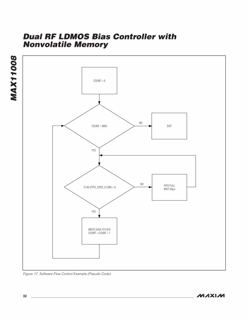
MA
X1
10
08
Dual RF LDMOS Bias Controller withNonvolatile Memory
32 ______________________________________________________________________________________
FLAG (FIFO_OVER_FLOW) = 0
WRITE DATA TO FIFOCOUNT = COUNT + 1
FIFO FULLWAIT 60µs
YES
NO
COUNT = 0
COUNT < MAX EXIT
YES
NO
Figure 17. Software Flow Control Example (Pseudo Code)

MA
X1
10
08
Dual RF LDMOS Bias Controller withNonvolatile Memory
______________________________________________________________________________________ 33
ALARM = 1
WRITE DATA TO FIFOCOUNT = COUNT + 1
FIFO FULLWAIT 60µs
YES
NO
COUNT = 0
COUNT < MAX EXIT
YES
NO
Figure 18. Hardware Flow Control Example (Pseudo Code)

MA
X1
10
08 high until the current scan is complete and the ADC
sequence halts. In single-conversion mode (CKSEL1,CKSEL0 = 11), the BUSY signal remains high until theADC has completed the current conversion (not theentire scan), the data has been moved into the FIFO,and the alarm limits for the channel have been checked(if alarm is enabled).
Alarm FunctionThe MAX11008 features a multipurpose alarm functionthat indicates when a temperature sensor or a current-sense amplifier reading exceeds the threshold valuesspecified in the High Temperature Threshold, LowTemperature Threshold, High Current Threshold, andLow Current Threshold registers (see Tables 7 to 10).The thresholds for each temperature sensor and cur-rent-sense amplifier channel are set individually andcan be configured to operate in window mode or hys-teresis mode (see the Window Mode and HysteresisMode sections). Alarm indication is provided by theALARM output while information on the source of thealarm is contained in the Flag register (see Table 26).The enabling of the various alarms, the polarity of theALARM output (active-high or active-low), the ALARM-output modes, the alarm-threshold modes, and themethods by which the MAX11008 services an alarm arecontrolled with the Alarm Software Configuration regis-ter and Alarm Hardware Configuration register (seeTables 12 and 14).
ALARM-Output ModesThe ALARM output operates in comparator mode orinterrupt mode based on the setting of the ACOMP bit(D8) in the Alarm Hardware Configuration register (seeTable 14).
When configured for comparator mode, the ALARMoutput is asserted when the measured current or tem-perature value exceeds the set threshold level and isdeasserted when the value returns below the setthreshold level.
When configured for interrupt mode, the ALARM outputis asserted when the measured current/temperaturevalue exceeds the set threshold level and remainsasserted until the Flag register is read, at which timethe ALARM output is deasserted. The alarm output isonly asserted again if the alarm channel recovers andthen re-trips (or if a different alarm channel trips).
See Figures 19 and 20 for examples of both ALARM-output modes.
Window ModeSet the TWIN1 bit (D2) or TWIN2 bit (D6) to 1 in theAlarm Software Configuration register (see Table 12) to
configure the temperature alarm thresholds for channel 1or channel 2 to window mode. Set the IWIN1 bit (D0) orIWIN2 bit (D4) to 1 in the Alarm Software Configurationregister to set the current alarm thresholds for channel 1or channel 2 to window mode. In window mode, temper-ature/current measurements are compared to the settemperature/current high and low thresholds. If a mea-sured value is outside the configured window values(between the set high and low thresholds) and that cor-responding channel is configured to cause an alarmcondition, the alarm asserts. The alarm remains internallyasserted until the measured values from that channel fallback into the window and past the configurable hystere-sis. The external behavior of ALARM and the gateclamps are controlled by the settings of the ACOMP andALMCLMP_ bits in the Alarm Hardware Configurationregister. The amount of built-in hysteresis can be variedfrom 8 LSBs to 64 LSBs by setting ALMHYST[1:0] bits(D6 and D7) in the Alarm Hardware Configuration regis-ter (see Tables 14 and 14a). See Figures 19 and 20 forwindow-mode threshold examples.
Hysteresis ModeSet the TWIN1 bit (D2) or TWIN2 bit (D6) to 0 in theAlarm Software Configuration register (see Table 12) toset the temperature alarm thresholds for channel 1 orchannel 2 to hysteresis mode. Set the IWIN1 bit (D0) orIWIN2 bit (D4) to 0 to set the current alarm thresholdsfor channel 1 or channel 2 to hysteresis mode. In hys-teresis mode, temperature or current measurementsare compared to the set temperature/current high andlow thresholds. If a measured value is above the sethigh threshold and the corresponding channel is con-figured to cause an alarm condition, the alarm asserts.ALARM remains internally asserted until the measuredvalues from that channel fall back below the low thresh-old setting. The external behavior of ALARM and thegate clamps are controlled by the settings of theACOMP and ALMCLMP_ bits in the Alarm HardwareConfiguration register. See Figures 21 and 22 for hys-teresis-mode threshold examples.
VGATE_ Output EquationBased on the monitored LDMOS current analog inputvoltage and temperature values, the MAX11008 logicallydecides if the calculated bias voltage, VGATE_, driving thegate of the RF LDMOS, should be recalculated andadjusted to maintain the desired RF LDMOS drain cur-rent. The MAX11008 independently monitors and calcu-lates the VGATE_ voltage for both channel 1 and channel2. The MAX11008 implements the following equationwhen calculating VGATE_ for each DAC channel:
Dual RF LDMOS Bias Controller withNonvolatile Memory
34 ______________________________________________________________________________________
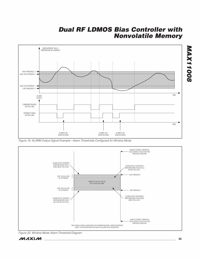
MA
X1
10
08
Dual RF LDMOS Bias Controller withNonvolatile Memory
______________________________________________________________________________________ 35
(MEASUREMENT VALUETEMPERATURE OR CURRENT)
HIGH THRESHOLD
COMPARATOR MODE(ACTIVE LOW)
INTERRUPT MODE(ACTIVE LOW)
BUILT-IN HYSTERESIS
LOW THRESHOLD
ALARMOUTPUT
TIME
TIME
BUILT-IN HYSTERESIS
ALARM FLAG REGISTER READ
ALARM FLAG REGISTER READ
ALARM FLAG REGISTER READ
Figure 19. ALARM Output Signal Example—Alarm Thresholds Configured for Window Mode
HIGHEST POSSIBLE THRESHOLDVALUE (DEFAULT VALUE FOR HIGH
THRESHOLD REGISTER)
LOWEST POSSIBLE THRESHOLDVALUE (DEFAULT VALUE FOR LOW
THRESHOLD REGISTER)
HIGH THRESHOLD
LOW THRESHOLD
RANGE OF VALUES THAT DONOT CAUSE AN ALARM
ALARM OUTPUT DEASSERTEDWHEN MEASURED VALUE FALLS
BELOW THIS LEVEL*
ALARM OUTPUT DEASSERTEDWHEN MEASURED VALUE RISES
ABOVE THIS LEVEL*ALARM OUTPUT ASSERTEDWHEN MEASURED VALUEFALLS BELOW THIS LEVEL
*ONLY WHEN ALARM IS CONFIGURED FOR COMPARATOR MODE. WHEN IN INTERRUPTMODE, FLAG REGISTER MUST BE READ FOR ALARM TO BE DEASSERTED.
BUILT-IN 8–64 LSBsOF HYSTERESIS
BUILT-IN 8–64 LSBsOF HYSTERESIS
ALARM OUTPUT ASSERTEDWHEN MEASURED VALUERISES ABOVE THIS LEVEL
Figure 20. Window-Mode Alarm-Threshold Diagram

MA
X1
10
08
Dual RF LDMOS Bias Controller withNonvolatile Memory
36 ______________________________________________________________________________________
HIGH THRESHOLD
TIME
LOW THRESHOLD
TIMEALARM OUTPUT
COMPARATOR MODE(ACTIVE LOW)
INTERRUPT MODE(ACTIVE LOW)
MEASUREMENT VALUE(TEMPERATURE OR CURRENT)
ALARM FLAGREGISTER
READ
ALARM FLAGREGISTER
READ
Figure 21. ALARM Output Signal Example—Alarm Thresholds Configured for Hysteresis Mode
HIGHEST POSSIBLE THRESHOLDVALUE (DEFAULT VALUE FOR HIGH
THRESHOLD REGISTER)
HIGH THRESHOLD
LOW THRESHOLD
LOWEST POSSIBLE THRESHOLDVALUE (DEFAULT VALUE FOR LOW
THRESHOLD REGISTER)
RANGE OF VALUES THAT WILLNOT CAUSE AN ALARM
ALARM OUTPUT ASSERTEDWHEN MEASURED VALUE
FALLS BELOW THIS LEVEL*
ALARM OUTPUT ASSERTEDWHEN MEASURED VALUERISES ABOVE THIS LEVEL
*ONLY WHEN ALARM IS CONFIGURED FOR COMPARATOR MODE. WHEN IN INTERRUPTMODE, FLAG REGISTER MUST BE READ FOR ALARM TO BE DEASSERTED.
Figure 22. ALARM Output Signal Example—Alarm Thresholds Configured for Hysteresis Mode

VGATE_ = (2 x VREFDAC x CODE)/4096
= [2 x VREFDAC x (VSET_ + LUTTEMPTemp +LUTAPCAPC)]/4096
where:
VGATE_ = actual gate voltage.
VSET_ = factory-set DAC code at TCAL.
LUTTEMPTemp = interpolated lookup value in theTEMP table for the sampled temperature.
LUTAPCAPC = interpolated lookup value in the APCtable for the APC parameter.
TCAL = temperature at which LUTTEMPTCAL returns0; i.e., the calibration temperature.
VSET_ is a 12-bit unsigned DAC code (0 to 4095).LUTTEMPTemp and LUTAPCAPC are the result oflookup operations and are 16-bit signed numbers inDAC CODE units. The MAX11008 calculates the sum of(VSET_ + LUTTEMPTemp + LUTAPCAPC) with 16-bitsigned arithmetic and limits that result to the 12-bit res-olution of the DAC (0 to 4095) to arrive at the final out-put DAC CODE.
The LUT values for Temp (LUTTEMPTemp) and APC(LUTAPCAPC) are the result of lookup table opera-tions (LUT operations). The values are directly stored inthe LUT sections of the EEPROM. They are 16-bitsigned (two’s complement) quantities, but to preventmathematical overflow, their magnitude should be limit-ed to 12-bit quantities (-4096 to +4095, which is the fullrange of the DAC ignoring the sign).
When averaging is disabled, VGATE_ operations pro-ceed as follows:
1) A new ADC sample is measured and compared tothe last sample used for a VGATE_ calculation.
2) The absolute difference between the two ADC mea-surements is compared to the hysteresis setting. Ifthe difference is equal to or greater than the hystere-sis setting, the new sample is used to recalculateVGATE_. If the hysteresis setting is not exceeded, thefollowing steps are bypassed and VGATE_ is notrecalculated.
3) The ADC sample is converted to a pointer for theLUT. The mechanism for this is explained in the fol-lowing section, but the process turns the 12-bit ADCsample into an n-bit pointer.
4) The lookup operation is performed, and if required,an interpolation between two table values is calcu-lated. The result from the lookup table is stored aseither LUTTEMPTemp or LUTAPCAPC.
5) The VGATE_ equation is now calculated anddepending on the status of the LDAC_ bit, output tothe appropriate DAC. The actual value of the DACoutput depends on the values within the LUT. It ispossible that the new value for VGATE_ is the sameas the last value for VGATE_, even though the hys-teresis in step 2 was exceeded.
If averaging is enabled for either the temperature orAPC parameter, the VGATE_ calculation process is thesame. The difference is that the value for the ADC sam-ple (step 1 and step 3) is replaced by an ADC average.The MAX11008 measures 16 samples to acquire an ini-tial average. When averaging is enabled, the first 15samples do not trigger a new average, and a VGATE_calculation is not triggered. After the average isacquired, each new ADC sample produces a newrolling average. The rolling average is calculated withthe following equations.
In acquire mode:
Average is only valid after 16 samples.
In tracking mode:
Average = 15/16 Average + 1/16 Sample
= 15/16 Average + 1/16 (Average + Difference)
where:
Difference = Sample - Average
= Average + 1/16 Difference
= Average + 1/16 (Limited Difference)
The limited difference between the sample and theaverage is a maximum value that is set by the T_LIMITand A_LIMIT bits, which are used to reject spuriousnoise. Difference limiting may be set from 1 LSB to 64LSBs, or may be disabled altogether.
By setting the A_AVGCTL and T_AVGCTL bits, theaverage tracking formula can be altered to add 1/4 ofthe difference on each calculation, rather than 1/16.This reduces the filter’s time constant and allows theaverage to track faster moving signals, and is mostsuited to the APC channel. The A_AVGCTL andT_AVGCTL bits do not alter the formula for acquiringthe initial average.
If the APC[11:0] value is used instead of an ADC sam-ple for the APC sample, all averaging and hysteresisfunctions are bypassed. The serial interface directlycontrols the APC[11:0] value and triggers a VGATE_ cal-culation each time it is written.
Average Samplej
= ∑=
/160
15
MA
X1
10
08
Dual RF LDMOS Bias Controller withNonvolatile Memory
______________________________________________________________________________________ 37
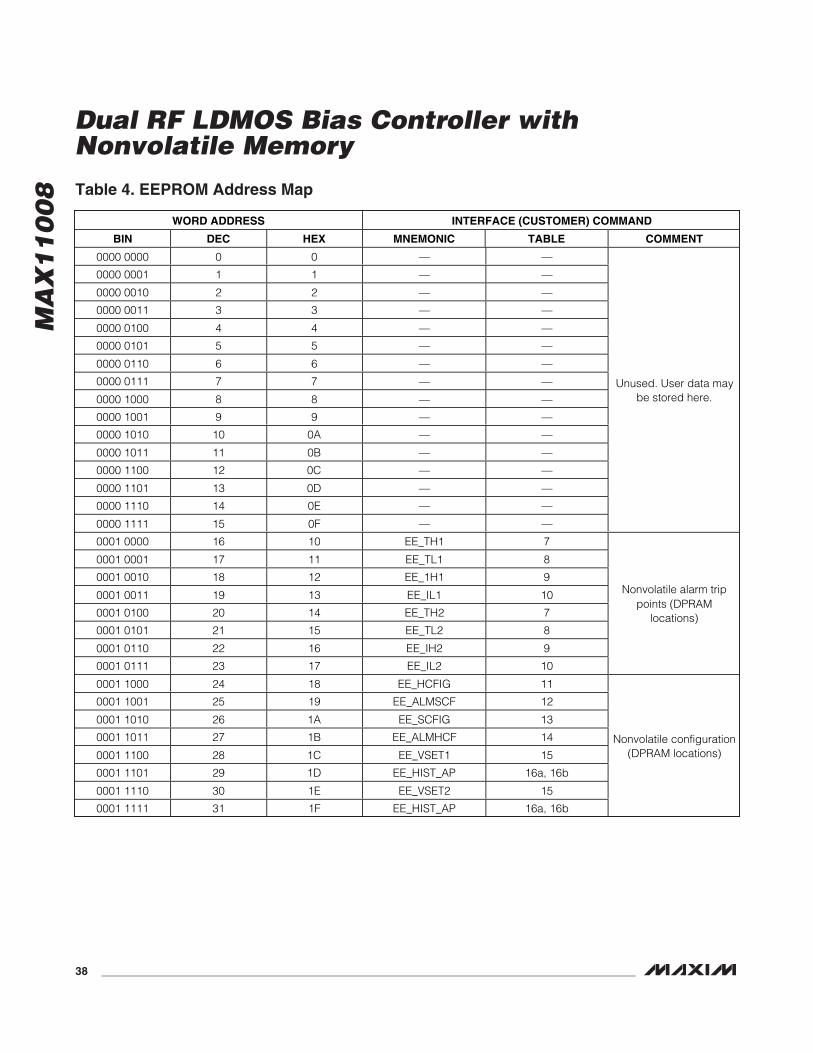
MA
X1
10
08
Dual RF LDMOS Bias Controller withNonvolatile Memory
38 ______________________________________________________________________________________
WORD ADDRESS INTERFACE (CUSTOMER) COMMAND
BIN DEC HEX MNEMONIC TABLE COMMENT
0000 0000 0 0 — —
0000 0001 1 1 — —
0000 0010 2 2 — —
0000 0011 3 3 — —
0000 0100 4 4 — —
0000 0101 5 5 — —
0000 0110 6 6 — —
0000 0111 7 7 — —
0000 1000 8 8 — —
0000 1001 9 9 — —
0000 1010 10 0A — —
0000 1011 11 0B — —
0000 1100 12 0C — —
0000 1101 13 0D — —
0000 1110 14 0E — —
0000 1111 15 0F — —
Unused. User data maybe stored here.
0001 0000 16 10 EE_TH1 7
0001 0001 17 11 EE_TL1 8
0001 0010 18 12 EE_1H1 9
0001 0011 19 13 EE_IL1 10
0001 0100 20 14 EE_TH2 7
0001 0101 21 15 EE_TL2 8
0001 0110 22 16 EE_IH2 9
0001 0111 23 17 EE_IL2 10
Nonvolatile alarm trippoints (DPRAM
locations)
0001 1000 24 18 EE_HCFIG 11
0001 1001 25 19 EE_ALMSCF 12
0001 1010 26 1A EE_SCFIG 13
0001 1011 27 1B EE_ALMHCF 14
0001 1100 28 1C EE_VSET1 15
0001 1101 29 1D EE_HIST_AP 16a, 16b
0001 1110 30 1E EE_VSET2 15
0001 1111 31 1F EE_HIST_AP 16a, 16b
Nonvolatile configuration(DPRAM locations)
Table 4. EEPROM Address Map
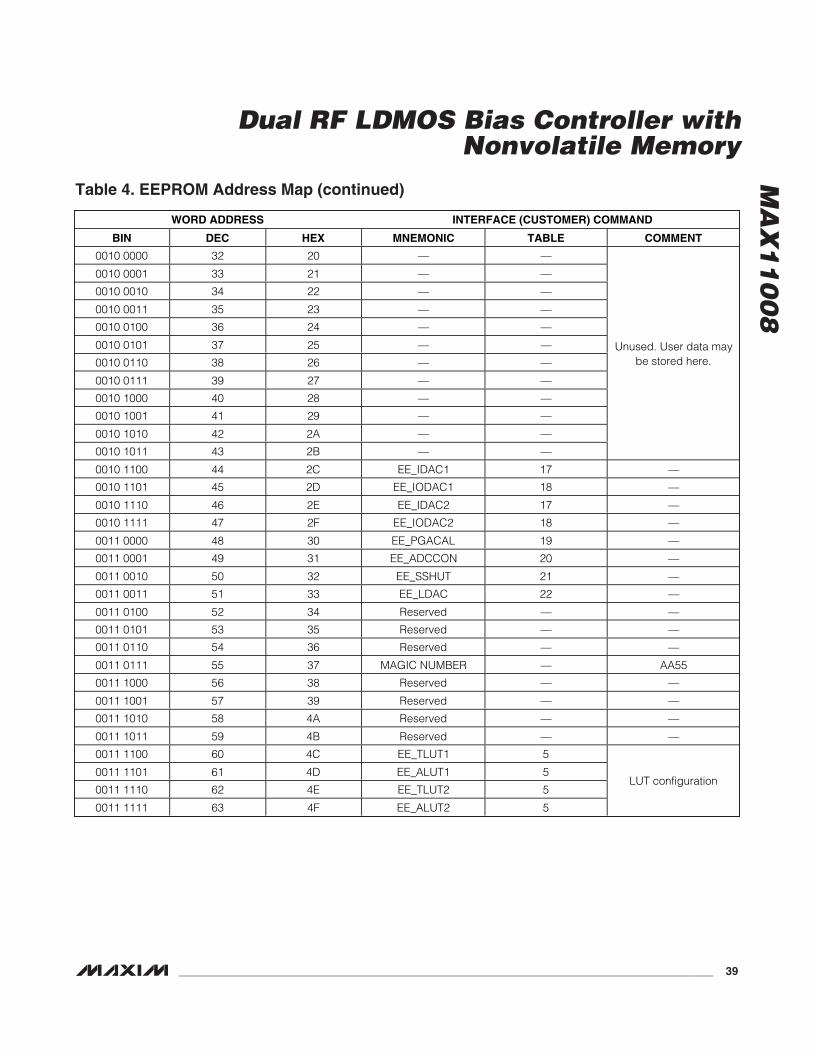
MA
X1
10
08
Dual RF LDMOS Bias Controller withNonvolatile Memory
______________________________________________________________________________________ 39
WORD ADDRESS INTERFACE (CUSTOMER) COMMAND
BIN DEC HEX MNEMONIC TABLE COMMENT
0010 0000 32 20 — —
0010 0001 33 21 — —
0010 0010 34 22 — —
0010 0011 35 23 — —
0010 0100 36 24 — —
0010 0101 37 25 — —
0010 0110 38 26 — —
0010 0111 39 27 — —
0010 1000 40 28 — —
0010 1001 41 29 — —
0010 1010 42 2A — —
0010 1011 43 2B — —
Unused. User data maybe stored here.
0010 1100 44 2C EE_IDAC1 17 —
0010 1101 45 2D EE_IODAC1 18 —
0010 1110 46 2E EE_IDAC2 17 —
0010 1111 47 2F EE_IODAC2 18 —
0011 0000 48 30 EE_PGACAL 19 —
0011 0001 49 31 EE_ADCCON 20 —
0011 0010 50 32 EE_SSHUT 21 —
0011 0011 51 33 EE_LDAC 22 —
0011 0100 52 34 Reserved — —
0011 0101 53 35 Reserved — —
0011 0110 54 36 Reserved — —
0011 0111 55 37 MAGIC NUMBER — AA55
0011 1000 56 38 Reserved — —
0011 1001 57 39 Reserved — —
0011 1010 58 4A Reserved — —
0011 1011 59 4B Reserved — —
0011 1100 60 4C EE_TLUT1 5
0011 1101 61 4D EE_ALUT1 5
0011 1110 62 4E EE_TLUT2 5
0011 1111 63 4F EE_ALUT2 5
LUT configuration
Table 4. EEPROM Address Map (continued)

MA
X1
10
08 EEPROM
The MAX11008 features 4Kb of EEPROM capable ofstoring up to 256 16-bit data words. The first 64 datawords of the EEPROM contain configuration data (seeTable 4) while the remaining 192 data words are pro-grammable and used for storing temperature and APCLUTs. The MAX11008 utilizes the LUT values to performgate voltage calculations (see the VGATE_ OutputEquation section). See the First-In-First-Out (FIFO), LUTStreaming Mode, and Message Mode sections for moreinformation on how to program and read from theEEPROM. See the Temperature/APC LUT ConfigurationRegisters section for information on how to configurethe LUTs and how values are retrieved from the LUTsfor VGATE_ calculations. See Table 5.
Nonvolatile Initialization ValuesUpon power-on reset, the data contained within specif-ic EEPROM locations is copied directly to correspond-ing locations within the register address mapdepending on the state of the magic number (see theMagic Number section).
• Locations 0x10–0x1F are directly copied to their cor-responding locations within the register addressmap.
• Locations 0x2C–0x33 are conditionally copied totheir corresponding locations within the registeraddress map. Set the MSB (labeled WCTRAM) to 1for locations 0x2C–0x33 to be copied to the registeraddress map (see Table 4a).
By correctly configuring the initialization values storedwithin the EEPROM, the MAX11008 can automaticallyenter VGATE_ compensation mode without the need fora host processor. This autonomous operation is usefulin some application areas where a host controller is notdesired.
Changes made to the working registers during opera-tion are volatile. To change a register’s nonvolatile ini-tialization value, the corresponding EEPROM locationmust be written by the LUT streaming protocol.
Magic NumberThe address location 0x37 of the EEPROM is referredto as the magic address. If the magic address is pro-grammed with the magic number (0xAA55), the valuesstored in address locations 0x10–0x1F and 0x2C–0x33are loaded into the working registers (see the RegisterAddress Map section) during power-up initialization.Address locations 0x10–0x1F are unconditionallyloaded into the working registers, whereas addresslocations 0x2C–0x33 are only loaded if bit D15(WCTRAM) of the address is set to 1. If magic addresslocation 0x37 is not programmed with the magic num-ber (0xAA55), the EEPROM is determined to be unpro-grammed; the power-up initialization load is thenbypassed and the working registers default to theirpower-on reset value.
LUT ValuesThe values stored within the LUT section of theEEPROM are 16-bit signed (two’s complement)
Dual RF LDMOS Bias Controller withNonvolatile Memory
40 ______________________________________________________________________________________
HEX MNEMONIC TABLE BIT 15 BIT 14 BIT 13 BIT 12 BIT 11 BIT 10 BIT 9 BIT 8 BIT 7 BIT 6 BIT 5 BIT 4 BIT 3 BIT 2 BIT 1 BIT 0
10 EE_TH1 7 X X X X D11 D10 D9 D8 D7 D6 D5 D4 D3 D2 D1 D0
11 EE_TL1 8 X X X X D11 D10 D9 D8 D7 D6 D5 D4 D3 D2 D1 D0
12 EE_IH1 9 X X X X D11 D10 D9 D8 D7 D6 D5 D4 D3 D2 D1 D0
13 EE_IL1 10 X X X X D11 D10 D9 D8 D7 D6 D5 D4 D3 D2 D1 D0
14 EE_TH2 7 X X X X D11 D10 D9 D8 D7 D6 D5 D4 D3 D2 D1 D0
15 EE_TL2 8 X X X X D11 D10 D9 D8 D7 D6 D5 D4 D3 D2 D1 D0
16 EE_IH2 9 X X X X D11 D10 D9 D8 D7 D6 D5 D4 D3 D2 D1 D0
17 EE_IL2 10 X X X X D11 D10 D9 D8 D7 D6 D5 D4 D3 D2 D1 D0
18 EE_HCFIG 11 T1AVGCTL T1LIMIT2 T1LIMIT1 T1LIMIT0 FIFOSTAT ADCMON PG2SET1 PG2SET0 PG1SET1 PG1SET1 CKSEL1 CKSEL0 ADCREF1 ADCREF0 DACREF1 DACREF0
19 EE_ALMSCF 12 X X X X A2AVG T2AVG A1AVG T1AVG TALARM2 TWIN2 IALARM2 IWIN2 TALARM1 TWIN1 IALARM1 IWIN1
1A EE_SCFIG 13 T2AVGCTL T2LIMIT2 T2LIMIT1 T1LIMIT0 LDAC2 TCOMP2 APCCOMP2 TSRC2 APCSRC21 APCSRC20 LDAC1 TCOMP1 APCCOMP1 TSRC1 APCSRC11 APCSRC10
1B EE_ALMHCF 14 X X X X X AVGMON INTEMP2 ALMCMP ALMHYST1 ALMHYST0 ALMCLMP21 ALMCLMP20 ALMCLMP11 ALMCLMP10 ALMPOL ALMOPN
1C EE_VSET1 15 X X X X D11 D10 D9 D8 D7 D6 D5 D4 D3 D2 D1 D0
1D EE_HIST_AP 16a T1HIST3 T1HIST2 T1HIST1 T1HIST0 D11 D10 D9 D8 D7 D6 D5 D4 D3 D2 D1 D0
1D EE_HIST_AP 16b T1HIST3 T1HIST2 T1HIST1 T1HIST0 X X X X A1AVGCTL A1LIMIT2 A1LIMIT1 A1LIMIT0 A1HIST3 A1HIST2 A1HIST1 A1HIST0
1E EE_VSET2 15 X X X X D11 D10 D9 D8 D7 D6 D5 D4 D3 D2 D1 D0
1F EE_HIST_AP 16a T1HIST3 T1HIST2 T1HIST1 T1HIST0 D11 D10 D9 D8 D7 D6 D5 D4 D3 D2 D1 D0
1F EE_HIST_AP 16b T2HIST3 T2HIST2 T2HIST2 T2HIST0 X X X X A2AVGCTL A2LIMIT2 A2LIMIT1 A2LIMIT0 A2HIST3 A2HIST2 A2HIST1 A2HIST0
2C EE_IDAC1 17 WCTRAM X X X D11 D10 D9 D8 D7 D6 D5 D4 D3 D2 D1 D0
2D EE_IODAC1 18 WCTRAM X X X D11 D10 D9 D8 D7 D6 D5 D4 D3 D2 D1 D0
2E EE_IDAC2 17 WCTRAM X X X D11 D10 D9 D8 D7 D6 D5 D4 D3 D2 D1 D0
2F EE_IODAC2 18 WCTRAM X X X D11 D10 D9 D8 D7 D6 D5 D4 D3 D2 D1 D0
30 EE_PGACAL 19 WCTRAM X X X X X X X X X X X X TRACK DOCAL SELFTIME
31 EE_ADCCON 20 WCTRAM X X X X X X X CONCONV ADCIN2 CS2 EXTTEMP2 ADCIN1 CS1 EXTEMP1 INTEMP
32 EE_SSHUT 21 WCTRAM X X X X X X X X X X X FBGON OSCPD DAC2PD DAC1PD
33 EE_LDAC 22 WCTRAM X X X X X X X X X X X X X DAC_CH2 DAC_CH1
37 MAGIC NUMBER — 1 0 1 0 1 0 1 0 0 1 0 1 0 1 0 1
3C EE_TLUT1 5 POFF5 POFF4 POFF3 POFF2 POFF1 POFF0 INT1 INT0 PSIZE1 PSIZE0 TSIZE2 TSIZE1 TSIZE0 SOT2 SOT1 SOT0
3D EE_ALUT1 5 POFF5 POFF4 POFF3 POFF2 POFF1 POFF0 INT1 INT0 PSIZE1 PSIZE0 TSIZE2 TSIZE1 TSIZE0 SOT2 SOT1 SOT0
3E EE_TLUT2 5 POFF5 POFF4 POFF3 POFF2 POFF1 POFF0 INT1 INT0 PSIZE1 PSIZE0 TSIZE2 TSIZE1 TSIZE0 SOT2 SOT1 SOT0
3F EE_ALUT2 5 POFF5 POFF4 POFF3 POFF2 POFF1 POFF0 INT1 INT0 PSIZE1 PSIZE0 TSIZE2 TSIZE1 TSIZE0 SOT2 SOT1 SOT0
Table 4a. EEPROM Address Bit Map

MA
X1
10
08
Dual RF LDMOS Bias Controller withNonvolatile Memory
______________________________________________________________________________________ 41
quantities. But to avoid the possibility of mathematicaloverflow, the magnitude of the values should be limitedto 12 bits (-4096 to +4095, which allows full movementover the range of the 12-bit DAC).
Temperature/APC LUT Configuration RegistersThe LUT Configuration register (see Table 5) specifiesthe location and the size of the temperature and auto-matic power control (APC) LUTs. The EEPROM can beconfigured to have a total of four LUTs (one tempera-ture LUT for each temperature-sensor channel and oneAPC LUT for each DAC channel). These registers canonly be programmed when the device is in LUT stream-ing mode and are set while data is being streamed intothe LUT. The data contained in the LUT Configurationregisters is stored in the EEPROM.
When VGATE_ calculations are made using temperatureand/or APC LUT values, the MAX11008 uses a LUTpointer to retrieve the correct values for the calculation.The LUT pointer value is derived from the most recent12-bit ADC measurement or directly transferred fromthe APC Parameter register (see Table 16). The sourceof the LUT pointer value depends on the settings of theSoftware Configuration register (see Table 13). PSIZEdetermines the size of the LUT pointer (see Table 5a).TSIZE specifies the size of the table (see Table 5c). It ispermissible to use an LUT pointer that is larger than thetable indexed. An 8-bit pointer functions properly with aLUT of 32 data locations. The LUT pointer values thatextend beyond the table are limited to the upper (orlower) bound of the table. This technique increases theeffective table resolution when the dynamic range ofADC samples is limited.
The POFF bits set the offset value that is added to theresulting LUT pointer value. POFF is a signed 6-bit valuethat is used to apply both positive and negative offsetvalues to the LUT pointer. The range of acceptable off-set values depends on PSIZE (see Table 5a). POFF istypically used for temperature LUTs that have LUT datafor 0°C measurements located at the center of the LUT.For example, if a temperature LUT has 64 data locations(locations 0 through 63), the data for 0°C is located atthe center of the LUT (location 31). If a temperaturemeasurement is made at 0°C, the resulting ADC conver-sion is 0, which instructs the LUT pointer to retrieve datafrom the first location (location 0) in the LUT. To retrievethe correct data for 0°C (location 31), a pointer offset of31 needs to be added to the LUT pointer.
To increase the accuracy of VGATE_ calculations, theMAX11008 can linearly interpolate intermediate temper-ature and APC compensation values from the two clos-est LUT data locations. To accomplish this, fractionalbits are added to the LUT pointer by setting the INT bits
(see Table 5b). When INT = 00 the LUT pointer has nofractional bits and no interpolation is performed. WhenINT = 00, every LUT pointer corresponds directly to atable entry. If INT = 01, the LUT pointer has 1 fractionalbit, which represents a fractional 1/2. This representsan LUT pointer that falls midway between two tableentries, and the MAX11008 performs a linear interpola-tion between those two entries. Similarly, INT = 10 pro-vides 2 fractional bits (1/4 resolution or 4:1interpolation), and INT = 11 provides 3 fractional bits(1/8 resolution or 8:1 interpolation). See the Calculatingan LUT Pointer from an ADC Sample/APC Parametersection for a detailed description and examples on cal-culating LUT pointer values.
The SOT bits set the starting addresses of each corre-sponding LUT in the EEPROM (see Table 5d). Eachtable starts at one of six possible locations within theEEPROM memory space. It is also possible to makeseveral LUT tables occupy the same memory spacewithin the EEPROM by simply setting identical SOT val-ues. This is useful when temperature or APC data iscommon to both channels. This allows a single sharedtable of double the resolution to be implementedinstead of two separate identical tables.
Tables 5e and 5f contain examples on how to configurethe LUTs in EEPROM using the TSIZE, SOT, andPSIZE bits.
Calculating an LUT Pointer from an ADCSample/APC Parameter
Calculate the LUT pointer value using the followingsteps:
1) The 12-bit ADC value is first shifted to the right bythe number of bits as determined by the followingequation:
12-bit ADC value right shift = 7 - PSIZE - INT
where PSIZE and INT are the decimal values ofPSIZE and INT in the LUT Configuration register. TheLUT pointer is interpreted as a fixed-point fractionalnumber where PSIZE specifies the number of inte-ger bits and INT specifies the number of fractionalbits.
2) The pointer offset value is left-shifted in the followingmanner:
If PSIZE = 00 or 01, no shifting is performed.
If PSIZE = 10, POFF is shifted to the left by 1 bit.
If PSIZE = 11, POFF is shifted to the left by 2 bits.
POFF is interpreted as a signed number.
3) The resulting POFF value is added to the LUT point-er value.

MA
X1
10
08
Dual RF LDMOS Bias Controller withNonvolatile Memory
42 ______________________________________________________________________________________
4) The resulting LUT pointer value is bound-limited toensure it fits within the corresponding LUT. Negativepointer values are limited to zero, and pointer valuesthat extend beyond the range of the LUT are limitedto the last entry.
5) The final LUT pointer value is calculated by shiftingSOT to the left by 5 bits and then adding it to thecurrent LUT pointer value. If no linear interpolation(INT = 00) is to be performed, the resulting LUTpointer value is equal to the absolute EEPROMaddress from which the LUT data is retrieved. If lin-ear interpolation is to be performed (INT = 01, 10, or11), the two LUT addresses that are closest to theresulting LUT pointer value and their correspondingdata values are entered into the following equationto calculate the interpolated data value that is usedin the VGATE_ calculation:
where PTR is the calculated LUT pointer value withfractional bits, ADD1 and ADD2 are the two LUTaddresses closest to the value of PTR, and DATA1 andDATA2 are the LUT data values stored at ADD1 andADD2.
LUT Pointer Example 1 (No Interpolation)POFF = 001000 (offset of +8).
INT = 00 (no interpolation/LUT pointer does not haveany fractional bits).
PSIZE = 00 (5-bit LUT pointer not including any frac-tional bits).
TSIZE = 001 (LUT has 32 data locations).
SOT = 010 (LUT starts at EEPROM address 40 hex).
Interpolated Data DATAPTR ADD
ADD ADDx DATA DATA
( )= +−
−⎛⎝⎜
⎞⎠⎟ −1
12 1
2 1
DATABITS
BITNAME
RESETSTATE
FUNCTION
D [ 15:10] POFF 000000 POFF bits.
D[9:8] INT 00Interpolation degree select bits.See Table 5b.
D[7:6] PSIZE 00LUT pointer size bit. See Table5a.
D[5:3] TSIZE 000 LUT size bit. See Table 5c.
D[2:0] SOT 000Start of table address bits. SeeTable 5d.
Table 5. Temperature/APC LUTConfiguration Register
PSIZE LUT POINTER SIZE POFF OFFSET RANGE*
005-bit pointer (access upto 32 data locations)
-32 to +31
016-bit pointer (access upto 64 data locations)
-32 to +31
107-bit pointer (access upto 128 data locations)
-64 to +62 (in steps of 2)
118-bit pointer (access upto 256 data locations)
- 128 to + 124 ( i n step s of 4)
Table 5a. LUT Pointer Sizes and OffsetRanges
INTNUMBER OF FRACTIONAL BITS ADDED TO
LUT POINTER00 001 1 ≥ 1:2 interpolation10 2 ≥ 1:4 interpolation11 3 ≥ 1:8 interpolation
Table 5b. Fractional Bits Added to LUTPointer for Linear Interpolation
*POFF is either a negative or positive number. When POFF isnegative its value is represented in two’s complement format.
TSIZE LUT SIZE
000 Unused
001 Table size of 32 data locations
010 Table size of 64 data locations
011 Table size of 96 data locations
100 Table size of 128 data locations
101 Table size of 160 data locations
110 Table size of 192 data locations
111 Unused
Table 5c. Selectable LUT Sizes
SOT STARTING ADDRESS IN EEPROM (HEX)
000 Unused
001 Unused
010 0x40
011 0x60
100 0x80
101 0xA0
110 0xC0
111 0xE0
Table 5d. Selectable LUT StartingAddresses
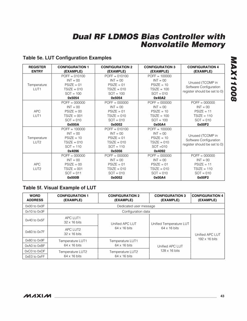
MA
X1
10
08
Dual RF LDMOS Bias Controller withNonvolatile Memory
______________________________________________________________________________________ 43
REGISTERENTRY
CONFIGURATION 1(EXAMPLE)
CONFIGURATION 2(EXAMPLE)
CONFIGURATION 3(EXAMPLE)
CONFIGURATION 4(EXAMPLE)
TemperatureLUT1
POFF = 010100INT = 00
PSIZE = 01TSIZE = 010SOT = 100
0x5054
POFF = 010100INT = 00
PSIZE = 01TSIZE = 010SOT = 100
0x5054
POFF = 100000INT = 00
PSIZE = 10TSIZE = 100SOT = 010
0x40A2
Unused (TCOMP inSoftware Configuration
register should be set to 0)
APCLUT1
POFF = 000000INT = 00
PSIZE = 00TSIZE = 001SOT = 010
0x000A
POFF = 000000INT = 00
PSIZE = 01TSIZE = 010SOT = 010
0x0052
POFF = 000000INT = 00
PSIZE = 10TSIZE = 100SOT = 100
0x00A4
POFF = 000000INT = 00
PSIZE = 11TSIZE = 110SOT = 010
0x00F2
TemperatureLUT2
POFF = 100000INT = 00
PSIZE = 10TSIZE = 010SOT = 110
0x4096
POFF = 010100INT = 00
PSIZE = 01TSIZE = 010SOT = 110
0x5056
POFF = 100000INT = 00
PSIZE = 10TSIZE = 010SOT =010
0x4092
Unused (TCOMP inSoftware Configuration
register should be set to 0)
APCLUT2
POFF = 000000INT = 00
PSIZE = 00TSIZE = 001SOT = 011
0x000B
POFF = 000000INT = 00
PSIZE = 01TSIZE = 010SOT = 010
0x0052
POFF = 000000INT = 00
PSIZE = 01TSIZE = 010SOT = 010
0x00A4
POFF = 000000INT = 00
PSIZE = 11TSIZE = 110SOT = 010
0x00F2
Table 5e. LUT Configuration Examples
WORDADDRESS
CONFIGURATION 1(EXAMPLE)
CONFIGURATION 2(EXAMPLE)
CONFIGURATION 3(EXAMPLE)
CONFIGURATION 4(EXAMPLE)
0x00 to 0x0F Dedicated user message
0x10 to 0x3F Configuration data
0x40 to 0x5FAPC LUT132 x 16 bits
0x60 to 0x7FAPC LUT232 x 16 bits
Unified APC LUT64 x 16 bits
Unified Temperature LUT64 x 16 bits
0x80 to 0x9F
0xA0 to 0xBFTemperature LUT1
64 x 16 bitsTemperature LUT1
64 x 16 bits
0xC0 to 0xDF
0xE0 to 0xFFTemperature LUT2
64 x 16 bitsTemperature LUT2
64 x 16 bits
Unified APC LUT128 x 16 bits
Unified APC LUT192 x 16 bits
Table 5f. Visual Example of LUT
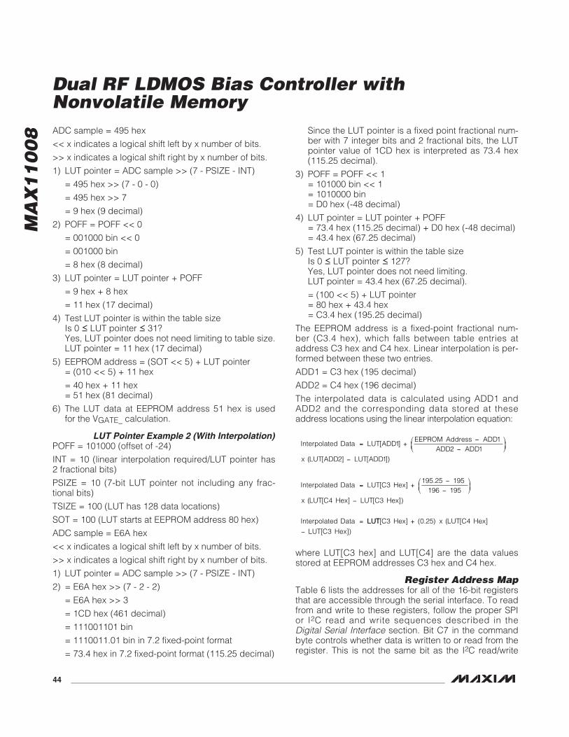
MA
X1
10
08
Dual RF LDMOS Bias Controller withNonvolatile Memory
44 ______________________________________________________________________________________
ADC sample = 495 hex
<< x indicates a logical shift left by x number of bits.
>> x indicates a logical shift right by x number of bits.
1) LUT pointer = ADC sample >> (7 - PSIZE - INT)
= 495 hex >> (7 - 0 - 0)
= 495 hex >> 7
= 9 hex (9 decimal)
2) POFF = POFF << 0
= 001000 bin << 0
= 001000 bin
= 8 hex (8 decimal)
3) LUT pointer = LUT pointer + POFF
= 9 hex + 8 hex
= 11 hex (17 decimal)
4) Test LUT pointer is within the table sizeIs 0 ≤ LUT pointer ≤ 31? Yes, LUT pointer does not need limiting to table size.LUT pointer = 11 hex (17 decimal)
5) EEPROM address = (SOT << 5) + LUT pointer = (010 << 5) + 11 hex
= 40 hex + 11 hex = 51 hex (81 decimal)
6) The LUT data at EEPROM address 51 hex is usedfor the VGATE_ calculation.
LUT Pointer Example 2 (With Interpolation)POFF = 101000 (offset of -24)
INT = 10 (linear interpolation required/LUT pointer has2 fractional bits)
PSIZE = 10 (7-bit LUT pointer not including any frac-tional bits)
TSIZE = 100 (LUT has 128 data locations)
SOT = 100 (LUT starts at EEPROM address 80 hex)
ADC sample = E6A hex
<< x indicates a logical shift left by x number of bits.
>> x indicates a logical shift right by x number of bits.
1) LUT pointer = ADC sample >> (7 - PSIZE - INT)
2) = E6A hex >> (7 - 2 - 2)
= E6A hex >> 3
= 1CD hex (461 decimal)
= 111001101 bin
= 1110011.01 bin in 7.2 fixed-point format
= 73.4 hex in 7.2 fixed-point format (115.25 decimal)
Since the LUT pointer is a fixed point fractional num-ber with 7 integer bits and 2 fractional bits, the LUTpointer value of 1CD hex is interpreted as 73.4 hex(115.25 decimal).
3) POFF = POFF << 1 = 101000 bin << 1 = 1010000 bin= D0 hex (-48 decimal)
4) LUT pointer = LUT pointer + POFF = 73.4 hex (115.25 decimal) + D0 hex (-48 decimal) = 43.4 hex (67.25 decimal)
5) Test LUT pointer is within the table sizeIs 0 ≤ LUT pointer ≤ 127? Yes, LUT pointer does not need limiting.LUT pointer = 43.4 hex (67.25 decimal).
= (100 << 5) + LUT pointer = 80 hex + 43.4 hex = C3.4 hex (195.25 decimal)
The EEPROM address is a fixed-point fractional num-ber (C3.4 hex), which falls between table entries ataddress C3 hex and C4 hex. Linear interpolation is per-formed between these two entries.
ADD1 = C3 hex (195 decimal)
ADD2 = C4 hex (196 decimal)
The interpolated data is calculated using ADD1 andADD2 and the corresponding data stored at theseaddress locations using the linear interpolation equation:
where LUT[C3 hex] and LUT[C4] are the data valuesstored at EEPROM addresses C3 hex and C4 hex.
Register Address MapTable 6 lists the addresses for all of the 16-bit registersthat are accessible through the serial interface. To readfrom and write to these registers, follow the proper SPIor I2C read and write sequences described in theDigital Serial Interface section. Bit C7 in the commandbyte controls whether data is written to or read from theregister. This is not the same bit as the I2C read/write
Interpolated Data LUT ADDEEPROM Address ADD
ADD ADDx LUT ADD LUT ADD
Interpolated Data LUT C Hex
x LUT C Hex LUT C Hex
Interpolated Data
[ ]
( [ ] [ ])
[ ] .
( [ ] [ ])
= +−
−⎛⎝⎜
⎞⎠⎟
−
= +−
−⎛⎝⎜
⎞⎠⎟
−
=
11
2 12 1
3195 25 195
196 1954 3
LUTLUT C Hex x LUT C Hex
LUT C Hex
[ ] ( . ) ( [ ]
[ ])
3 0 25 4
3
+
−
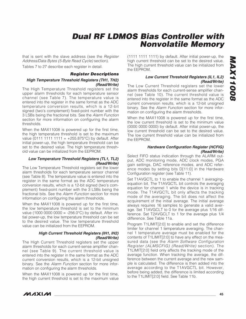
MA
X1
10
08
Dual RF LDMOS Bias Controller withNonvolatile Memory
______________________________________________________________________________________ 45
that is sent with the slave address (see the RegisterAddress/Data Bytes (5-Byte Read Cycle) section).
Tables 7 to 27 describe each register in detail.
Register DescriptionsHigh Temperature Threshold Registers (TH1, TH2)
(Read/Write)The High Temperature Threshold registers set theupper alarm thresholds for each temperature sensorchannel (see Table 7). The temperature value isentered into the register in the same format as the ADCtemperature conversion results, which is a 12-bitsigned (two’s complement) fixed-point number with the3 LSBs being the fractional bits. See the Alarm Functionsection for more information on configuring the alarmthresholds.
When the MAX11008 is powered up for the first time,the high temperature threshold is set to the maximumvalue (0111 1111 1111 = +255.875°C) by default. Afterinitial power-up, the high temperature threshold can beset to the desired value. The high temperature thresh-old value can be initialized from the EEPROM.
Low Temperature Threshold Registers (TL1, TL2)(Read/Write)
The Low Temperature Threshold registers set the loweralarm thresholds for each temperature sensor channel(see Table 8). The temperature value is entered into theregister in the same format as the ADC temperatureconversion results, which is a 12-bit signed (two’s com-plement) fixed-point number with the 3 LSBs being thefractional bits. See the Alarm Function section for moreinformation on configuring the alarm thresholds.
When the MAX11008 is powered up for the first time,the low temperature threshold is set to the minimumvalue (1000 0000 0000 = -256.0°C) by default. After ini-tial power-up, the low temperature threshold can be setto the desired value. The low temperature thresholdvalue can be initialized from the EEPROM.
High Current Threshold Registers (IH1, IH2)(Read/Write)
The High Current Threshold registers set the upperalarm thresholds for each current-sense amplifier chan-nel (see Table 9). The current threshold value isentered into the register in the same format as the ADCcurrent conversion results, which is a 12-bit unsignedbinary. See the Alarm Function section for more infor-mation on configuring the alarm thresholds.
When the MAX11008 is powered up for the first time,the high current threshold is set to the maximum value
(1111 1111 1111) by default. After initial power-up, thehigh current threshold can be set to the desired value.The high current threshold value can be initialized fromthe EEPROM.
Low Current Threshold Registers (IL1, IL2)(Read/Write)
The Low Current Threshold registers set the loweralarm thresholds for each current-sense amplifier chan-nel (see Table 10). The current threshold value isentered into the register in the same format as the ADCcurrent conversion results, which is a 12-bit unsignedbinary. See the Alarm Function section for more infor-mation on configuring the alarm thresholds.
When the MAX11008 is powered up for the first time,the low current threshold is set to the minimum value(0000 0000 0000) by default. After initial power-up, thelow current threshold can be set to the desired value.The low current threshold value can be initialized fromthe EEPROM.
Hardware Configuration Register (HCFIG)(Read/Write)
Select FIFO status indication through the ALARM out-put, ADC monitoring mode, ADC clock modes, PGAgain settings, DAC reference modes, and ADC refer-ence modes by setting bits D[11:0] in the HardwareConfiguration register (see Table 11).
Set T1AVGCTL to 1 to enable the channel 1 averaging-equation bit. The T1AVGCTL bit controls the averagingequation for channel 1 while the device is in trackingmode. The T1AVGCTL bit only affects the trackingmode of the averaging. The bit does not affect theacquirement of the initial average. The initial averagealways requires 16 samples to generate a valid aver-age. Set T1AVGCLT to 0 for the average plus 1/16 dif-ference. Set T2AVGCLT to 1 for the average plus 1/4difference. See Table 11a.
Program T1LIMIT[2:0] to enable and set the differencelimiter for channel 1 temperature averaging. The chan-nel 1 temperature average must be enabled for thecontents of T1LIMIT[2:0] to have any effect on the mea-sured data (see the Alarm Software ConfigurationRegister (ALMSCFIG) (Read/Write) section). TheT1LIMIT[2:0] field only affects the tracking mode of theaverage function. When tracking the average, the dif-ference between the current average and the new sam-ple is calculated. The difference is then added into theaverage according to the T1AVGCTL bit. However,before being added, the difference is limited accordingto the T1LIMIT[2:0] field. See Table 11b.
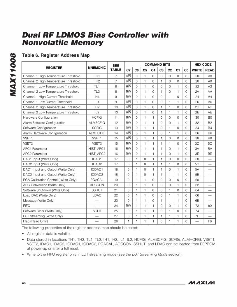
MA
X1
10
08
Dual RF LDMOS Bias Controller withNonvolatile Memory
46 ______________________________________________________________________________________
COMMAND BITS HEX CODEREGISTER MNEMONIC
SEETABLE C7 C6 C5 C4 C3 C2 C1 C0 WRITE READ
Channel 1 High Temperature Threshold TH1 7 RW 0 1 0 0 0 0 0 20 A0
Channel 2 High Temperature Threshold TH2 7 RW 0 1 0 1 0 0 0 28 A8
Channel 1 Low Temperature Threshold TL1 8 RW 0 1 0 0 0 1 0 22 A2
Channel 2 Low Temperature Threshold TL2 8 RW 0 1 0 1 0 1 0 2A AA
Channel 1 High Current Threshold IH1 9 RW 0 1 0 0 1 0 0 24 A4
Channel 1 Low Current Threshold IL1 9 RW 0 1 0 0 1 1 0 26 A6
Channel 2 High Temperature Threshold IH2 10 RW 0 1 0 1 1 0 0 2C AC
Channel 2 Low Temperature Threshold IL2 10 RW 0 1 0 1 1 1 0 2E AE
Hardware Configuration HCFIG 11 RW 0 1 1 0 0 0 0 30 B0
Alarm Software Configuration ALMSCFIG 12 RW 0 1 1 0 0 1 0 32 B2
Software Configuration SCFIG 13 RW 0 1 1 0 1 0 0 34 B4
Alarm Hardware Configuration ALMHCFIG 14 RW 0 1 1 0 1 1 0 36 B6
VSET1 VSET1 15 RW 0 1 1 1 0 0 0 38 B8
VSET2 VSET2 15 RW 0 1 1 1 1 0 0 3C BC
APC1 Parameter HIST_APC1 16 RW 0 1 1 1 0 1 0 3A BA
APC2 Parameter HIST_APC2 16 RW 0 1 1 1 0 1 0 3E BE
DAC1 Input (Write Only) IDAC1 17 0 1 0 1 1 0 0 0 58 —
DAC2 Input (Write Only) IDAC2 17 0 1 0 1 1 1 0 0 5C —
DAC1 Input and Output (Write Only) IODAC1 18 0 1 0 1 1 0 1 0 5A —
DAC2 Input and Output (Write Only) IODAC2 18 0 1 0 1 1 1 1 0 5E —
PGA Calibration Control ( Write Only) PGACAL 19 0 1 1 0 0 0 0 0 60 —
ADC Conversion (Write Only) ADCCON 20 0 1 1 0 0 0 1 0 62 —
Software Shutdown (Write Only) SSHUT 21 0 1 1 0 0 1 0 0 64 —
Load DAC (Write Only) LDAC 22 0 1 1 0 0 1 1 0 66 —
Message (Write Only) — 23 0 1 1 0 1 1 1 0 6E —
FIFO — 24 RW 1 1 1 0 0 1 0 72 80
Software Clear (Write Only) SCLR 25 0 1 1 1 0 1 0 0 74 —
LUT Streaming (Write Only) — 27 0 1 1 1 1 1 1 0 7E —
Flag (Read Only) — 26 1 1 1 1 0 1 1 0 — F6
Table 6. Register Address Map
The following properties of the register address map should be noted:
• All register data is volatile.
• Data stored in locations TH1, TH2, TL1, TL2, IH1, IH2, IL1, IL2, HCFIG, ALMSCFIG, SCFIG, ALMHCFIG, VSET1,VSET2, IDAC1, IDAC2, IODAC1, IODAC2, PGACAL, ADCCON, SSHUT, and LDAC can be loaded from EEPROMat power-up or after a full reset.
• Write to the FIFO register only in LUT streaming mode (see the LUT Streaming Mode section).

MA
X1
10
08
Dual RF LDMOS Bias Controller withNonvolatile Memory
______________________________________________________________________________________ 47
Set FIFOSTAT to 1 to use the ALARM output to monitorthe data flow of the FIFO while in LUT streaming modeor message mode. See the LUT Streaming Mode andMessage Mode sections for more information on thesemodes of operation and how to use the ALARM outputfor FIFO flow control.
Set ADCMON to 1 to copy ADC conversion results intothe FIFO where it can be read out through the serialinterface. See the ADC Monitoring Mode section formore information on reading conversion results fromthe FIFO. ADCMON and AVGMON cannot be active atthe same time.
Program PG_SET[1:0] to set the channel 1 and channel2 current-sense amplifier gain (see Table 11c).
Program CKSEL[1:0] to set the conversion and acquisi-tion timing clock modes (see Table 11d). See theInternally Timed Acquisitions and Conversions sectionfor detailed descriptions of each clock mode.
Program ADCREF[1:0] to establish the source of theADC reference (see Table 11e). Program theDACREF[1:0] to establish the source of the DAC refer-ence (see Table 11f). See the ADC and DACReferences section for more information on configuringthe data converter references.
Alarm Software Configuration Register (ALMSCFIG)(Read/Write)
Configure the software alarm functions with bits D[11:0]in the Alarm Software Configuration register (see Table12). Bits D[15:12] are don’t-care bits.
Set A_AVG to 1 to enable the APC averaging and filter-ing function for channel 1 and channel 2. TheAPCSRC_ field in the SCFG register controls the sourceof the sample.
DATA BITS BIT NAME RESET STATE FUNCTION
D[15:12] Unused X Unused bits.
D[11:D0] THI[11:0] 0111 1111 1111 High temperature threshold data bits.
Table 7. High Temperature Threshold Register
DATA BITS BIT NAME RESET STATE FUNCTION
D[15:12] Unused X Unused bits.
D[11:0] TLO[11:0] 1000 0000 0000 Low temperature threshold data bits.
Table 8. Low Temperature Threshold Register
X = Don’t care.
X = Don’t care.
DATA BITS BIT NAME RESET STATE FUNCTION
D[15:12] Unused X Unused bits.
D[11:0] IHI[11:0] 1111 1111 1111 High current threshold data bits.
Table 9. High Current Threshold Register
X = Don’t care.
DATA BITS BIT NAME RESET STATE FUNCTION
D[15:12] Unused X Unused bits.
D[11:0] ILO[11:0] 0000 0000 0000 Low current threshold data bits.
Table 10. Low Current Threshold Register
X = Don’t care.
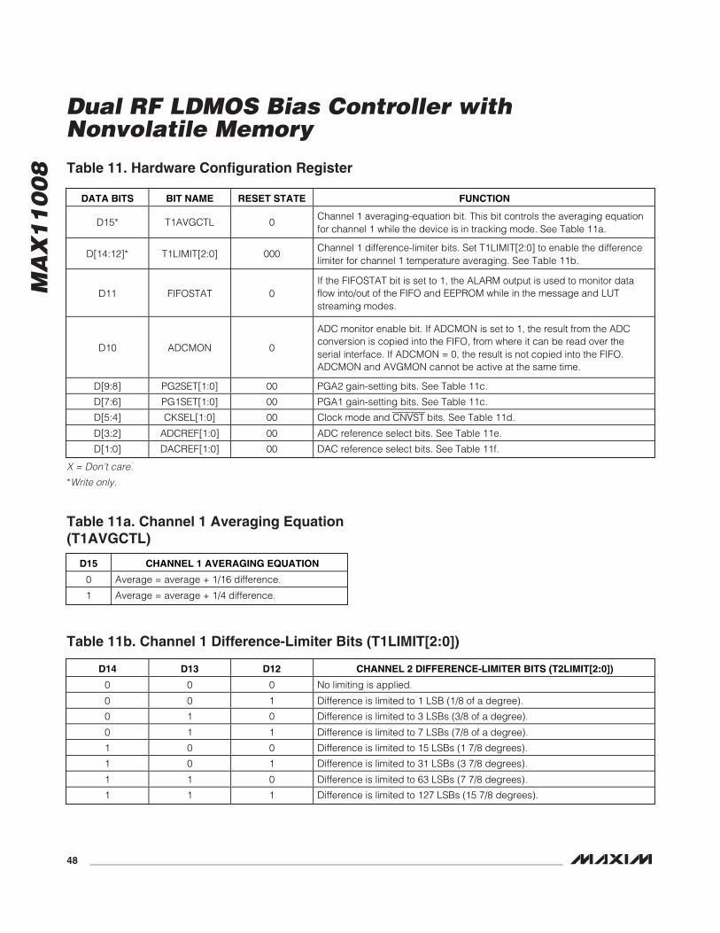
MA
X1
10
08
Dual RF LDMOS Bias Controller withNonvolatile Memory
48 ______________________________________________________________________________________
DATA BITS BIT NAME RESET STATE FUNCTION
D15* T1AVGCTL 0Channel 1 averaging-equation bit. This bit controls the averaging equationfor channel 1 while the device is in tracking mode. See Table 11a.
D[14:12]* T1LIMIT[2:0] 000Channel 1 difference-limiter bits. Set T1LIMIT[2:0] to enable the differencelimiter for channel 1 temperature averaging. See Table 11b.
D11 FIFOSTAT 0If the FIFOSTAT bit is set to 1, the ALARM output is used to monitor dataflow into/out of the FIFO and EEPROM while in the message and LUTstreaming modes.
D10 ADCMON 0
ADC monitor enable bit. If ADCMON is set to 1, the result from the ADCconversion is copied into the FIFO, from where it can be read over theserial interface. If ADCMON = 0, the result is not copied into the FIFO.ADCMON and AVGMON cannot be active at the same time.
D[9:8] PG2SET[1:0] 00 PGA2 gain-setting bits. See Table 11c.
D[7:6] PG1SET[1:0] 00 PGA1 gain-setting bits. See Table 11c.
D[5:4] CKSEL[1:0] 00 Clock mode and CNVST bits. See Table 11d.
D[3:2] ADCREF[1:0] 00 ADC reference select bits. See Table 11e.
D[1:0] DACREF[1:0] 00 DAC reference select bits. See Table 11f.
Table 11. Hardware Configuration Register
X = Don’t care.
*Write only.
D15 CHANNEL 1 AVERAGING EQUATION
0 Average = average + 1/16 difference.
1 Average = average + 1/4 difference.
Table 11a. Channel 1 Averaging Equation(T1AVGCTL)
D14 D13 D12 CHANNEL 2 DIFFERENCE-LIMITER BITS (T2LIMIT[2:0])
0 0 0 No limiting is applied.
0 0 1 Difference is limited to 1 LSB (1/8 of a degree).
0 1 0 Difference is limited to 3 LSBs (3/8 of a degree).
0 1 1 Difference is limited to 7 LSBs (7/8 of a degree).
1 0 0 Difference is limited to 15 LSBs (1 7/8 degrees).
1 0 1 Difference is limited to 31 LSBs (3 7/8 degrees).
1 1 0 Difference is limited to 63 LSBs (7 7/8 degrees).
1 1 1 Difference is limited to 127 LSBs (15 7/8 degrees).
Table 11b. Channel 1 Difference-Limiter Bits (T1LIMIT[2:0])
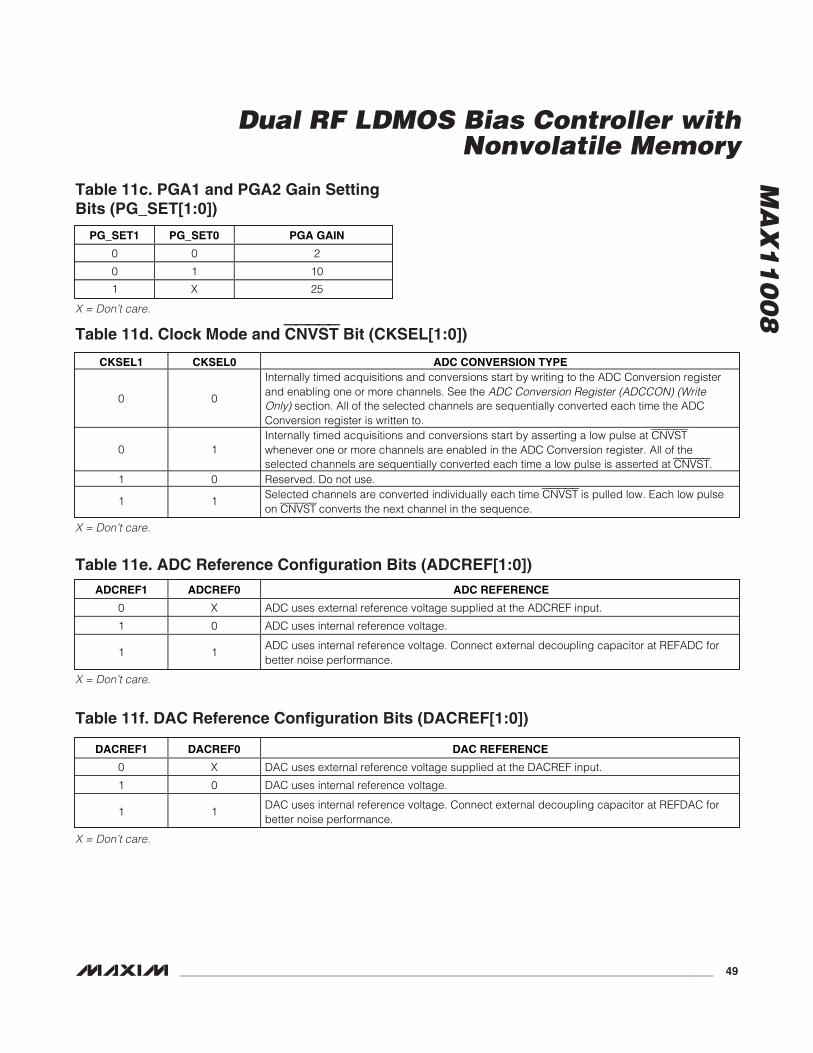
MA
X1
10
08
Dual RF LDMOS Bias Controller withNonvolatile Memory
______________________________________________________________________________________ 49
PG_SET1 PG_SET0 PGA GAIN
0 0 2
0 1 10
1 X 25
Table 11c. PGA1 and PGA2 Gain SettingBits (PG_SET[1:0])
CKSEL1 CKSEL0 ADC CONVERSION TYPE
0 0
Internally timed acquisitions and conversions start by writing to the ADC Conversion registerand enabling one or more channels. See the ADC Conversion Register (ADCCON) (WriteOnly) section. All of the selected channels are sequentially converted each time the ADCConversion register is written to.
0 1Internally timed acquisitions and conversions start by asserting a low pulse at CNVSTwhenever one or more channels are enabled in the ADC Conversion register. All of theselected channels are sequentially converted each time a low pulse is asserted at CNVST.
1 0 Reserved. Do not use.
1 1Selected channels are converted individually each time CNVST is pulled low. Each low pulseon CNVST converts the next channel in the sequence.
Table 11d. Clock Mode and CNVST Bit (CKSEL[1:0])
ADCREF1 ADCREF0 ADC REFERENCE
0 X ADC uses external reference voltage supplied at the ADCREF input.
1 0 ADC uses internal reference voltage.
1 1ADC uses internal reference voltage. Connect external decoupling capacitor at REFADC forbetter noise performance.
Table 11e. ADC Reference Configuration Bits (ADCREF[1:0])
X = Don’t care.
X = Don’t care.
DACREF1 DACREF0 DAC REFERENCE
0 X DAC uses external reference voltage supplied at the DACREF input.
1 0 DAC uses internal reference voltage.
1 1DAC uses internal reference voltage. Connect external decoupling capacitor at REFDAC forbetter noise performance.
Table 11f. DAC Reference Configuration Bits (DACREF[1:0])
X = Don’t care.
X = Don’t care.

MA
X1
10
08
Dual RF LDMOS Bias Controller withNonvolatile Memory
50 ______________________________________________________________________________________
Set T_AVG to 1 to enable the temperature averagingand filtering function for channel 1 and channel 2. TheTSRC_ field in the SCFG register controls the source ofthe sample.
Set TALARM_ to 1 to enable and to 0 to disable thealarm function for channel 1 and channel 2 temperaturemeasurements.
Set TWIN_ to 0 to configure the channel 1 and channel 2temperature alarms for hysteresis mode, and set TWIN_to 1 to configure the channel 1 and channel 2 tempera-ture alarms for window mode. See the Hysteresis Modeand Window Mode sections for detailed descriptions ofeach alarm mode. Use the Alarm HardwareConfiguration register to set the value of hysteresis whenin window mode (see Tables 14 and 14a).
Set IALARM_ to 1 to enable and to 0 to disable thealarm function for channel 1 and channel 2 currentmeasurements.
Set IWIN_ to 0 to configure the channel 1 and channel2 current-sense alarm for hysteresis mode, and setIWIN_ to 1 to configure the channel 1 and channel 2current-sense alarm for window mode. See theHysteresis Mode and Window Mode sections fordetailed descriptions of each alarm mode. Use the AlarmHardware Configuration register to set the value of hys-teresis when in window mode (see Tables 14 and 14a).
Software Configuration Register (SCFIG)(Read/Write)
Bits D[15:0] in the Software Configuration register (seeTable 13) control the parameters that trigger VGATE_calculations, how the results of the VGATE_ calculationare applied (APC and/or temperature compensation),and whether the calculation result is written to the DACinput register only or to both input and output registers.The register also determines the source of the APC andtemperature parameters, which are used to calculatethe LUT pointer for retrieving LUT values (see theTemperature/APC LUT Configuration Registers sec-tion). The data stored in the Software Configuration reg-ister can be initialized from the EEPROM. Table 13dsummarizes all of the possible VGATE_ calculation trig-ger conditions that can be set by the SoftwareConfiguration register.
Set T2AVGCTL to 1 to enable the channel 2 averaging-equation bit. The T2AVGCTL bit controls the averagingequation for channel 2 while the device is in trackingmode. The T2AVGCTL bit only affects the trackingmode of the averaging. The bit does not affect the
acquirement of the initial average. The initial averagealways requires 16 samples to generate a valid aver-age. Set T2AVGCLT to 0 for average plus 1/16 of thedifference. Set T2AVGCLT to 1 for average plus 1/4 ofthe difference. See Table 13a.
Program T2LIMIT[2:0] to enable and set the differencelimiter for channel 2 temperature averaging. The chan-nel 2 temperature average must be enabled for thecontents of the T2LIMIT[2:0] field to have any effect onthe measured data (see the Alarm SoftwareConfiguration Register (ALMSCFIG) (Read/Write) sec-tion). The T2LIMIT[2:0] field only affects the trackingmode of the average function. When tracking the aver-age, the difference between the current average andthe new sample is calculated. The difference is thenadded into the average according to the T2AVGCTLbit, but before being added the difference is limitedaccording to the T2LIMIT[2:0] field. See Table 13b.
Set LDAC_ to 0 to load the VGATE_ calculation resultinto the channel 1 and channel 2 DAC input and outputregisters, forcing the VGATE_ output to change as soonas the VGATE_ calculation is completed. Set LDAC_ to 1to load the calculation result into the channel 1 andchannel 2 DAC input registers. Transfer the results fromthe input register to the output register by writing to theLoad DAC register (see the Load DAC Register (LDAC)(Write Only) section).
Set TCOMP_ to 1 to allow VGATE_ calculations to betriggered by changes in channel 1 and channel 2 tem-perature measurements. In this mode, the VGATE_ cal-culation includes a temperature LUT value. Thetemperature measurement values that trigger VGATE_calculations depend on the settings of T_HIST[3:0] inthe APC Parameter register.
Set APCCOMP_ to 1 to allow VGATE_ calculations to betriggered by changes in channel 1 and channel 2 cur-rent-sense measurements or the APC parameter in theAPC Parameter register. In this mode, the VGATE_ cal-culation includes an APC LUT value. The current mea-surement values that trigger VGATE_ calculationsdepend on the settings of A_HIST[3:0] in the APCParameter register.
Set TSRC_ to 0 to use the channel 1 and channel 2external temperature sensor as the source of the temper-ature parameter for VGATE_ calculations. Set TSRC_ to 1to use the internal temperature sensor as the source ofthe temperature parameter for VGATE_ calculations.
Set APCSRC[1:0] to select the source of the APC para-meter used for VGATE_ calculations (see Table 13c).

MA
X1
10
08
Dual RF LDMOS Bias Controller withNonvolatile Memory
______________________________________________________________________________________ 51
Alarm Hardware Configuration Register(ALMHCFIG) (Read/Write)
Configure the hardware alarm functions with bitsD[10:0] in the Alarm Hardware Configuration register(see Table 14). Bits D[15:11] are don’t-care bits.
Set AVGMON to 1 to write ADC averages to the FIFO.The tracking average has a unique channel tag and isdistinguishable from the raw sample. The average mon-itoring is automatically suspended when in LUT stream-ing and message modes. ADCMON and AVGMONcannot be active at the same time.
Set INTEMP2 to 1 to configure the channel 2 tempera-ture alarm to monitor the internal temperature sensorreadings rather than the channel 2 external tempera-ture sensor. The status of the alarm is indicated by thechannel 2 temperature flags in the flag register. Thecurrent-sense alarm for channel 2 is no longer availablein this mode.
Set ALMCOMP to 1 to configure the ALARM output forcomparator mode, and set ALMCOMP to 0 to configurethe ALARM output for interrupt mode. See the ALARM-Output Modes section for a detailed description ofeach type of ALARM output mode.
Program ALMHYST[1:0] to set the amount of hysteresisthat is applied to the alarm thresholds when the alarmfunction is configured for window mode (see Table14a). See the Window Mode section for a detaileddescription of how the hysteresis is applied.
Set ALMCLMP[1:0] to control the methods to clamp theGATE_ to AGND when an alarm is triggered (see Table14b).
Set ALMPOL to 1 to configure the ALARM output to beactive-low, and set ALMPOL to 0 to configure theALARM output to be active-high.
Set ALMOPEN to 1 to configure the ALARM output foran open-drain output (pullup resistor required), and setALMOPEN to 0 for a push-pull output.
VSET Registers (VSET1, VSET2) (Read/Write)The VSET registers set the nominal GATE_ output codewithout any temperature or APC compensation (seeTable 15). This value is input into the VGATE_ calcula-tion (see the VGATE_ Output Equation section). Writingto this register triggers a VGATE_ calculation, and theresult of that calculation is loaded into either the DAC_input register or the DAC_ input and output registersdepending on the state of the LDAC_ bit in the SoftwareConfiguration register. Bits D[15:12] are don’t-care bits.
T_HIST_APC Registers (HIST_APC1, HIST_APC2)(Read/Write)
The T_HIST_APC registers are dual-functionality regis-ters. The function of the T_HIST_APC registersdepends upon the value of APCSRC_[1:0] bits in theSoftware Configuration register (see Table 13). IfAPCSRC_[1:0] = 00, the T_HIST_APC registers hold theAPC parameter and the temperature hysteresis controls(see Table 16a). If APCSRC_[1:0] = 10 or 11, theT_HIST_APC registers hold the APC averaging andhysteresis controls as well as temperature hysteresiscontrols (see Table 16b).
The T_HIST register bits T_HIST[3:0] set the temperaturehysteresis limits for both channel 1 and channel 2 VGATE_calculations. After a new temperature sample, the deviceproceeds in performing a VGATE_ calculation if that sam-ple differs from the previous sample used for a VGATE_calculation by an amount greater than the hysteresis set-ting (see Table 16c). Set APCCOMP_ and TCOMP_ to 0before T_HIST is changed.
The APC register bits (APC[11:0]) set the value that isconverted into the LUT pointer value, which is subse-quently used to retrieve the APC LUT value for VGATE_calculations (see Table 16a). This value is used onlywhen APCSRC_1 is set to 0 in the SoftwareConfiguration register. Writing to this register triggers aVGATE_ calculation when APCSRC_1 is set to 0 andAPCCOMP_ is set to 1 in the Software Configurationregister.
The A_AVGCTL bit controls the averaging equationfor APC while the device is in tracking mode. TheA_AVGCTL bit only affects the tracking mode of theaveraging. The bit does not affect the acquirementof the initial average. The initial average alwaysrequires 16 samples to generate a valid average. SetA_AVGCLT to 0 for average plus 1/16 of the difference.Set A_AVGCTL to 1 for average plus 1/4 of the differ-ence (see Table 16c).
Program A_LIMIT[2:0] to enable and set the differencelimiter for APC averaging. The APC average must beenabled for the contents of the A_LIMIT[2:0] field tohave any effect on the measured data. TheA_LIMIT[2:0] field only affects the tracking mode of theaverage function. When tracking the average, the dif-ference between the current average and the new sam-ple is calculated. The difference is then added into theaverage according to the A_AVGCTL bit, but beforebeing added the difference is limited according to theA_LIMIT[2:0] field (see Table 16d).
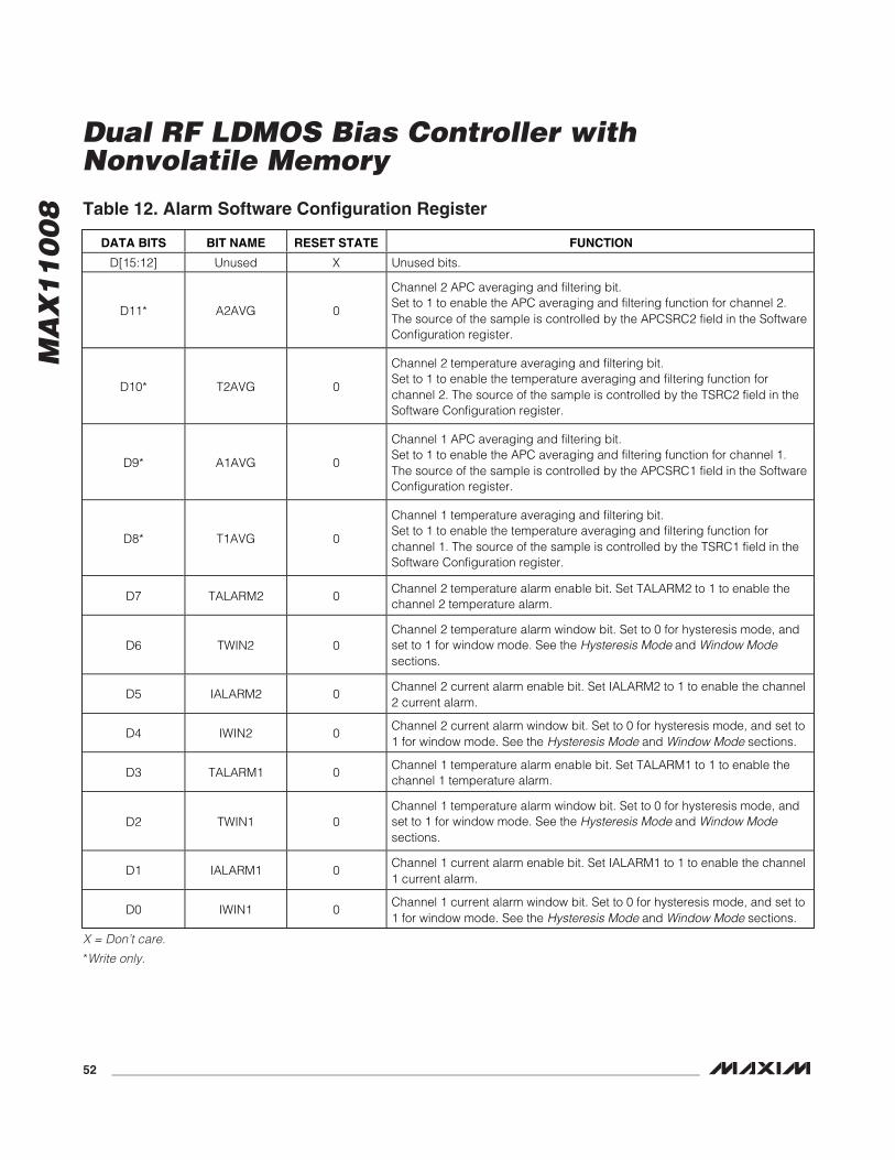
MA
X1
10
08
Dual RF LDMOS Bias Controller withNonvolatile Memory
52 ______________________________________________________________________________________
DATA BITS BIT NAME RESET STATE FUNCTION
D[15:12] Unused X Unused bits.
D11* A2AVG 0
Channel 2 APC averaging and filtering bit.Set to 1 to enable the APC averaging and filtering function for channel 2.The source of the sample is controlled by the APCSRC2 field in the SoftwareConfiguration register.
D10* T2AVG 0
Channel 2 temperature averaging and filtering bit.Set to 1 to enable the temperature averaging and filtering function forchannel 2. The source of the sample is controlled by the TSRC2 field in theSoftware Configuration register.
D9* A1AVG 0
Channel 1 APC averaging and filtering bit.Set to 1 to enable the APC averaging and filtering function for channel 1.The source of the sample is controlled by the APCSRC1 field in the SoftwareConfiguration register.
D8* T1AVG 0
Channel 1 temperature averaging and filtering bit.Set to 1 to enable the temperature averaging and filtering function forchannel 1. The source of the sample is controlled by the TSRC1 field in theSoftware Configuration register.
D7 TALARM2 0Channel 2 temperature alarm enable bit. Set TALARM2 to 1 to enable thechannel 2 temperature alarm.
D6 TWIN2 0Channel 2 temperature alarm window bit. Set to 0 for hysteresis mode, andset to 1 for window mode. See the Hysteresis Mode and Window Modesections.
D5 IALARM2 0Channel 2 current alarm enable bit. Set IALARM2 to 1 to enable the channel2 current alarm.
D4 IWIN2 0Channel 2 current alarm window bit. Set to 0 for hysteresis mode, and set to1 for window mode. See the Hysteresis Mode and Window Mode sections.
D3 TALARM1 0Channel 1 temperature alarm enable bit. Set TALARM1 to 1 to enable thechannel 1 temperature alarm.
D2 TWIN1 0Channel 1 temperature alarm window bit. Set to 0 for hysteresis mode, andset to 1 for window mode. See the Hysteresis Mode and Window Modesections.
D1 IALARM1 0Channel 1 current alarm enable bit. Set IALARM1 to 1 to enable the channel1 current alarm.
D0 IWIN1 0Channel 1 current alarm window bit. Set to 0 for hysteresis mode, and set to1 for window mode. See the Hysteresis Mode and Window Mode sections.
Table 12. Alarm Software Configuration Register
X = Don’t care.
*Write only.

MA
X1
10
08
Dual RF LDMOS Bias Controller withNonvolatile Memory
______________________________________________________________________________________ 53
DATA BITS BIT NAME RESET STATE FUNCTION
D15* T2AVGCTL 0Channel 2 averaging-equation bit. This bit controls the averaging equationfor channel 2 while the device is in tracking mode. See Table 13a.
D[14:12]* T2LIMIT[2:0] 000Channel 2 difference-limiter bits. Set T2LIMIT[2:0] to enable the differencelimiter for channel 2 temperature averaging. See Table 13b.
D11 LDAC2 0Channel 2 LDAC control bit. Set to 0 to load calculation results into the DAC2 input and output registers. Set to 1 to load calculation results into theDAC 2 input register only.
D10 TCOMP2 0Channel 2 temperature compensation enable bit. Set to 1 to allow VGATE2calculations to be triggered by channel 2 temperature measurements.
D9 APCCOMP2 0Channel 2 APC parameter compensation enable bit. Set to 1 to allowVGATE2 calculations to be triggered by channel 2 current-sensemeasurements or APC2 parameter changes.
D8 TSRC2 0Channel 2 temperature sensor select bit. Set to 0 to use the channel 2external temperature sensor as the source of the temperature parameter forVGATE2 calculations. Set to 1 to use the internal temperature sensor.
D[7:6] APCSRC2[1:0] 00Channel 2 APC parameter select bits. Set APCSRC2[1:0] to select the datasource for VGATE2 calculations. See Table 13c.
D5 LDAC1 0Channel 1 LDAC control bit. Set to 0 to load calculation results into the DAC1 input and output registers. Set to 1 to load calculation results into theDAC 1 input register only.
D4 TCOMP1 0Channel 1 temperature compensation enable bit. Set to 1 to allow VGATE1calculations to be triggered by channel 1 temperature measurements.
D3 APCCOMP1 0Channel 1 APC parameter compensation enable bit. Set to 1 to allowVGATE1 calculations to be triggered by channel 1 current-sensemeasurements or APC1 parameter changes.
D2 TSRC1 0Channel 1 temperature sensor select bit. Set to 0 to use the channel 1external temperature sensor as the source of the temperature parameter forVGATE1 calculations. Set to 1 to use the internal temperature sensor.
D[1:0] APCSRC1[1:0] 00Channel 1 APC parameter select bits. Set APCSRC1[1:0] to select the datasource for VGATE1 calculations. See Table 13c.
Table 13. Software Configuration Register
X = Don’t care.
*Write only.

MA
X1
10
08
Dual RF LDMOS Bias Controller withNonvolatile Memory
54 ______________________________________________________________________________________
The A_HIST register bits A_HIST[3:0] set the APC hys-teresis limits for both channel 1 and channel 2 VGATE_calculations. After a new APC sample, the device pro-ceeds in performing a VGATE_ calculation if that samplediffers from the previous sample used for a VGATE_ cal-culation by an amount greater than the hysteresis set-ting (see Table 16e). Set APCCOMP_ and TCOMP_ to 0before A_HIST is changed.
DAC Input Registers (IDAC1, IDAC2) (Write Only)DAC_[11:0] set the value of the DAC Input registers(see Table 17). Bits D[15:12] are don’t-care bits. TheGATE_ output is not updated with this value until it istransferred to the DAC Output register. Write to theLoad DAC register to transfer the contents of the DACInput register to the DAC Output register. Write directlyto the DAC Input register to manipulate the DAC outputwithout triggering a VGATE_ calculation.
DAC Input and Output Registers (IODAC1, IODAC2)(Write Only)
DAC_[11:0] set the values of the input and output regis-ters of the respective DACs (see Table 18). Writing to
this register does not trigger a VGATE_ calculation, butthe GATE_ output is immediately updated with thevalue that is written to this register. Bits D[15:12] aredon’t-care bits. The contents of the DAC Input andOutput registers are not stored in the EEPROM.
PGA Calibration Control Register (PGACAL)(Write Only)
The PGA Calibration Control register selects the PGAcalibration mode and controls when calibrations occur(see Table 19). Bits D[15:3] are don’t-care bits. Thedata contained in the PGA Calibration Control registeris stored in the EEPROM.
Set TRACK to 0 to perform the next PGA calibration inacquisition mode, and set TRACK to 1 to perform thenext PGA calibration in tracking mode. Leave TRACKset to 0 the first time a PGA calibration is performedafter power-up.
Set DOCAL to 1 to perform calibrations of PGA1 andPGA2. DOCAL resets to 0 after the PGA calibration rou-tine is complete. If either channel is powered down, thePGA calibration for that channel is bypassed.
D15 CHANNEL 2 AVERAGING EQUATION
0 Average = average + 1/16 difference.
1 Average = average + 1/4 difference.
Table 13a. Channel 2 Averaging Equation(T2AVGCTL)
D14 D13 D12 CHANNEL 2 DIFFERENCE LIMITER
0 0 0 No limiting is applied.
0 0 1 Difference is limited to 1 LSB (1/8 of a degree).
0 1 0 Difference is limited to 3 LSBs (3/8 of a degree).
0 1 1 Difference is limited to 7 LSBs (7/8 of a degree).
1 0 0 Difference is limited to 15 LSBs (1 7/8 degrees).
1 0 1 Difference is limited to 31 LSBs (3 7/8 degrees).
1 1 0 Difference is limited to 63 LSBs (7 7/8 degrees).
1 1 1 Difference is limited to 127 LSBs (15 7/8 degrees).
Table 13b. Channel 2 Difference Limiter Bits (T2LIMIT[2:0])
APCSRC_1 APCSRC_0 APC PARAMETER SOURCE SELECT
0 0 Value stored in APC parameter register.
0 1 Reserved. Do not use.
1 0 Drain current samples.
1 1 External input samples (AIN input).
Table 13c. APC Parameter Source Select Bits (APCSRC_1, APCSRC_0)
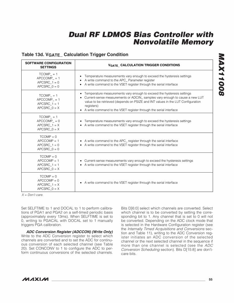
MA
X1
10
08
Dual RF LDMOS Bias Controller withNonvolatile Memory
______________________________________________________________________________________ 55
Set SELFTIME to 1 and DOCAL to 1 to perform calibra-tions of PGA1 and PGA2 on a self-timed periodic basis(approximately every 13ms). When SELFTIME is set to0, writing to PGACAL with DOCAL set to 1 manuallytriggers PGA calibration.
ADC Conversion Register (ADCCON) (Write Only)Write to the ADC Conversion register to select whichchannels are converted and to set the ADC for continu-ous conversion of each selected channel (see Table20). Set CONCONV to 1 to configure the ADC to per-form continuous conversions of the selected channels.
Bits D[6:0] select which channels are converted. Selectwhich channel is to be converted by setting the corre-sponding bit to 1. Any channel that is set to 0 will notbe converted. Depending on the ADC clock mode thatis selected in the Hardware Configuration register (seethe Internally Timed Acquisitions and Conversions sec-tion and Table 11), writing to the ADC Conversion reg-ister initiates an ADC conversion of the selectedchannel or the next selected channel in the sequence ifmore than one channel is selected (see the ADCConversion Scheduling section). Bits D[15:8] are don’t-care bits.
SOFTWARE CONFIGURATIONSETTINGS
VGATE_ CALCULATION TRIGGER CONDITIONS
TCOMP_ = 1APCCOMP_ = 1APCSRC_1 = 0APCSRC_0 = 0
• Temperature measurements vary enough to exceed the hysteresis settings• A write command to the APC_ Parameter register• A write command to the VSET register through the serial interface
TCOMP_ = 1APCCOMP_ = 1APCSRC_1 = 1APCSRC_0 = X
• Temperature measurements vary enough to exceed the hysteresis settings• Current-sense measurements or ADCIN_ samples vary enough to cause a new LUT
value to be retrieved (depends on PSIZE and INT values in the LUT Configurationregisters)
• A write command to the VSET register through the serial interface
TCOMP_ = 1APCCOMP_ = 0APCSRC_1 = XAPCSRC_0 = X
• Temperature measurements vary enough to exceed the hysteresis settings• A write command to the VSET register through the serial interface
TCOMP = 0APCCOMP = 1APCSRC_1 = 0APCSRC_0 = 0
• A write command to the APC_ register through the serial interface• A write command to the VSET register through the serial interface
TCOMP = 0APCCOMP = 1APCSRC_1 = 1APCSRC_0 = X
• Current-sense measurements vary enough to exceed the hysteresis settings• A write command to the VSET register through the serial interface
TCOMP = 0APCCOMP = 0APCSRC_1 = XAPCSRC_0 = X
• A write command to the VSET register through the serial interface
Table 13d. VGATE_ Calculation Trigger Condition
X = Don’t care.

MA
X1
10
08
Dual RF LDMOS Bias Controller withNonvolatile Memory
56 ______________________________________________________________________________________
Software Shutdown Register (SSHUT) (Write Only)Write to the Software Shutdown register to power downthe MAX11008 or specific sections of the MAX11008 tooptimize power consumption (see Table 21). BitsD[15:6] are don’t-care bits.
Set FULLPD to 1 to power down all sections of theMAX11008 except for the serial interface. FULLPDtakes precedence over all of the other power-downbits. Any commands (other than writing to the SoftwareShutdown register) sent to the MAX11008 while in fullpower-down mode are ignored. Set FULLPD to 0 to exitfull power-down mode.
Set FBGON to 1 to force the internal voltage referenceto remain powered up. This optimizes ADC conversiontimes since the internal voltage reference does notautomatically power down in between conversions(power-up time for internal reference is typically 50µs),but it also increases the power dissipation of theMAX11008. Set FBGON to 0 to power the internal volt-age reference on and off as required by the ADC.
Set WDGPD to 1 to power down the internal watchdogoscillator. The watchdog oscillator monitors the internalcircuit’s operation. It is not accessible outside of theMAX11008. Power down the internal watchdog ocillatorwhen entering LUS streaming mode.
DATA BITS BIT NAME RESET STATE FUNCTION
D[15:11] Unused XXXXX Unused bits.
D10* AVGMON 0
ADC average monitor enable bit. Set AVGMON to 1 to average the ADCsample. The ADC average is written to the FIFO. The tracking average has aunique channel tag and is distinguishable from the raw sample. The averagemonitoring is automatically suspended when in LUT streaming and messagemodes. ADCMON and AVGMON cannot be active at the same time.
D9 INTEMP2 0
Channel 2 temperature alarm select bit. Set to 1 to configure the channel 2temperature alarm to monitor the internal temperature sensor instead of theexternal temperature sensor. The status of the alarm is indicated by thechannel 2 temperature flags in the flag register. The current-sense alarm forchannel 2 is no longer available in this mode.
D8 ALMCOMP 0ALARM comparator enable bit. Set to 1 to configure the ALARM output forcomparator mode. Set to 0 to configure the ALARM output for interruptmode.
D[7:6] ALMHYST[1:0] 00 ALARM hysteresis select bits. See Table 14a.
D[5:4] ALMCLMP2[1:0 00 Channel 2 clamp-mode select bits. See Table 14b.
D[3:2] ALMCLMP1[1:0 00 Channel 1 clamp-mode select bits. See Table 14b.
D1 ALMPOL 0ALARM polarity select bit. Set to 1 to configure the ALARM output to beactive-low. Set to 0 for active-high.
D0 ALMOPEN 0ALARM output configuration select bit. Set to 1 for open-drain ALARMoutput. Set to 0 for push-pull ALARM output.
Table 14. Alarm Hardware Configuration Register
ALMHYST1 ALMHYST0 ALARM HYSTERESIS SELECT
0 0 8 LSBs of hysteresis (+1°C)
0 1 16 LSBs of hysteresis (+2°C)
1 0 32 LSBs of hysteresis (+4°C)
1 1 64 LSBs of hysteresis (+8°C)
Table 14a. ALARM Hysteresis Select Bits (ALMHYST[1:0])
X = Don’t care.
*Write-only.
MA
X1
10
08
Dual RF LDMOS Bias Controller withNonvolatile Memory
______________________________________________________________________________________ 57
Set OSCPD to 1 to power down the internal oscillator.When the internal oscillator is powered down, all inter-nal operations of the MAX11008 are suspended.OSCPD automatically resets back to 0 when the nextcommand is received by the serial interface.
Powering down the oscillator and leaving the watchdogoscillator powered up may allow the watchdog timer tooverflow. The overflow of the watchdog timer forces theMAX11008 to reset, reinitialize, and transmit a pulse onthe ALARM output.
Set DAC_PD to 1 to power down DAC_ and PGA_.Values can still be written to the DAC Input and Outputregisters when DAC_ is powered down.
Load DAC Register (LDAC) (Write Only)Write to the Load DAC register to transfer the contentsof the DAC input registers to the DAC output registers(see Table 22). The Load DAC register is a write-onlyregister that executes when written to, but does nothave storage. This function facilitates the simultaneousupdate of both DAC outputs. Set LDDACCH1 to 1 to
transfer the contents of the DAC1 Input register to theDAC1 Output register. Set LDDACCH2 to 1 to transferthe contents of the DAC2 Input register to the DAC2Output register. Bits D[15:2] are don’t-care bits.
Message Register (MR) (Write Only)Write to the Message register to place the MAX11008into message mode (see the Message Mode sectionand Table 23). MSGL[7:0] specifies the number of datawords (each data word is 16 bits long) to be read fromthe EEPROM. The message read from the EEPROM isbetween 1 and 256 words long. Write MSGL = 0 (deci-mal) to request a message length of 1, MSGL = 255(decimal) to request a message length of 256.MSGA[7:0] specifies the starting address of the mes-sage to be read from the EEPROM.
FIFO Register (FIFO) (Read/Write)When in message mode or ADC monitoring mode, theFIFO register is a read-only register (see Table 24). Inmessage mode, the specified EEPROM data words(each data word is 16 bits long) are copied into the
ALMCLMP1 ALMCLMP0 CLAMP MODE ALARM CLAMP SELECT
0 0 Alarm reportIf an alarm is triggered by a current or temperature conversion, the ALARMbit is set (1) in the alarm Flag register. No further action is taken.
0 1 Clamp gate The GATE_ output clamps to AGND immediately, independent of alarms.
1 0Clamp gate onalarm with clear
The GATE_ output is clamped to AGND in response to any alarm trip on thecorresponding channel. A subsequent ADC conversion, which shows thealarm condition has been removed, clears the clamp conditionautomatically.
1 1Clamp gate onalarm without
clear
The GATE_ output is clamped to AGND in response to any alarm trip on thecorresponding channel. The clamp does not clear automatically. If an alarmis triggered, the 11 value is overwritten to 01, causing a permanent clampcondition. A subsequent write to rest ALMCLMP[1:0] to 11 clears the clampcondition.
Table 14b. Clamp-Mode Select Bits (ALMCLMP[1:0])
DATA BITS BIT NAME RESET STATE FUNCTION
D[15:12] Unused 0000 Unused bits.
D[11:0] VSET_[11:0] NA VSET_ bits.
Table 15. VSET Registers
NA = Not applicable.

MA
X1
10
08
Dual RF LDMOS Bias Controller withNonvolatile Memory
58 ______________________________________________________________________________________
FIFO (see the Message Mode section) so that the datawords can be read out through the serial interface. Inmessage mode the FIFO is eight deep, and does notoverflow.
In ADC/average monitoring mode, the 12-bit ADC con-version results of each selected channel are copiedinto the FIFO so that the conversion results can be readout through the serial interface (see the ADC MonitoringMode section). Each conversion result includes a 4-bitchannel tag that indicates the source of the conversion(see Table 24a). In ADC/average monitoring mode the
FIFO is seven deep, and always contains the mostrecent seven data items. The oldest data placed intothe FIFO is always read out first.
When in LUT streaming mode, the FIFO register is awrite-only register. In LUT streaming mode, write thedata word that is to be written to the EEPROM into theFIFO register (see the LUT Streaming Mode section). Inthis mode the FIFO is eight deep, and is preventedfrom overflow. Data written to the FIFO when it is full isignored.
DATABITS
BIT NAME RESET STATE FUNCTION
D[15:12] T_HIST[3:0] 0000Hysteresis limit bits. The T_HIST[3:0] bits set the temperature hysteresis limits forboth channel 1 and channel 2 for VGATE_ calculations. See Table 14a.
D[11:0] APC[11:0] NA APC parameter bits.
Table 16a. APC Parameter Register (Valid when APCSRC[1:0] = 00)
NA = Not applicable.
DATA BITS BIT NAME RESET STATE FUNCTION
D[15:12] T_HIST[3:0] 0Temperature hysteresis limit bits. The T_HIST[3:0] bits set the temperaturehysteresis limits for both channel 1 and channel 2 for VGATE_ calculations. SeeTable 16c. Set APCCOMP_ and TCOMP_ to 0 before T_HIST is changed.
D[11:8] Unused NA —
D7 A_AVGCTL 0APC parameter bit. Controls the averaging equation for channel 1 andchannel 2. Set A_AVGCLT to 0 for average plus 1/16 difference. SetA_AVGCLT to 1 for average plus 1/4 difference.
D[6:4] A_LIMIT[2:0] 0APC difference limiter bits. Set A_LIMIT[2:0] to enable the difference limiter forchannel 1 and channel 2 APC averaging. See Table 16d.
D[3:0] A_HIST[3:0] 0APC hysteresis limit bits. The A_HIST[3:0] bits set the APC hysteresis limits forboth channel 1 and channel 2 for VGATE_ calculations. See Table 16e. SetAPCCOMP_ and TCOMP_ to 0 before A_HIST is changed.
Table 16b. APC Parameter Register (Valid when APCSRC[1:0] = 10 or 11)
MA
X1
10
08
Dual RF LDMOS Bias Controller withNonvolatile Memory
______________________________________________________________________________________ 59
TxHIST[3:0] FUNCTION
0000 1 LSB (1/8 of a degree). I.e., no hysteresis
0001 2 LSBs (1/4 of a degree)
0010 3 LSBs (3/8 of a degree)
0011 4 LSBs (1/2 of a degree)
0100 5 LSBs (5/8 of a degree)
0101 6 LSBs (3/4 of a degree)
0110 7 LSBs (7/8 of a degree)
0111 8 LSBs (1 degree)
1000 9 LSBs (1 1/8 of a degree)
1001 10 LSBs (1 1/4 of a degree)
1010 11 LSBs (1 3/8 of a degree)
1011 12 LSBs (1 1/2 of a degree)
1100 13 LSBs (1 5/8 of a degree)
1101 14 LSBs (1 3/4 of a degree)
1110 15 LSBs (1 7/8 of a degree)
1111 16 LSBs (2 degrees)
Table 16c. Temperature Hysteresis LimitRegister Bits
A_LIMIT[2:0] FUNCTION
000 No limiting is applied
001 D i ffer ence i s l i m i ted to 1 LS B ( 1/8 of a d eg r ee)
010 D i ffer ence i s l i m i ted to 3 LS Bs ( 3/8 of a d eg r ee)
011 D i ffer ence i s l i m i ted to 7 LS Bs ( 7/8 of a d eg r ee)
100 D i ffer ence i s l i m i ted to 15 LS Bs ( 1 7/8 d eg r ees)
101 D i ffer ence i s l i m i ted to 31 LS Bs ( 3 7/8 d eg r ees)
110 D i ffer ence i s l i m i ted to 63 LS Bs ( 7 7/8 d eg r ees)
111Difference is limited to 127 LSBs (15 7/8degrees)
Table 16d. APC Difference Limiter forAveraging
AxHIST[3:0] FUNCTION
0000 1 LSB. I.e., no hysteresis
0001 2 LSBs
0010 3 LSBs
0011 4 LSBs
0100 5 LSBs
0101 6 LSBs
0110 7 LSBs
0111 8 LSBs
1000 9 LSBs
1001 10 LSBs
1010 11 LSBs
1011 12 LSBs
1100 13 LSBs
1101 14 LSBs
1110 15 LSBs
1111 16 LSBs
Table 16e. APC Hysteresis LimitRegister Bits

MA
X1
10
08
Dual RF LDMOS Bias Controller withNonvolatile Memory
60 ______________________________________________________________________________________
Software Clear Register (SCLR) (Write Only)Write to the Software Clear register to clear the internalregisters with a single write command (see Table 25).Bits D[15:7] are don’t-care bits.
FULLRST and ARMRST operate in conjunction witheach other to allow a full hardware reset of the device.If ARMRST has been set to 1 by a previous write com-mand, setting FULLRST to 1 initiates a full reset of theMAX11008. ARMRST can only be set to 1 when theFULLRST is set to 0 in the same data word. This pro-vides protection from accidental resets since two writecommands are needed to initiate a full reset. To per-form a full reset, first write a data word with FULLRSTset to 0 and ARMRST set to 1. Then write another dataword with FULLRST set to 1 and ARMRST set to 0.
Set the ALMSCLR bit to 1 to clear all alarm thresholdregisters and their respective flags in the Flag register.
Set the AVGCLR bit to 1 to clear the average and hys-teresis memory for all lookup operations. Setting theAVGCLR bit reacquires the average and performs anew LUT operation.
Set FIFOCLR to 1 to clear the FIFO. This function isinstantaneous and does not affect BUSY.
Set DAC_RST to 1 to clear the contents of the DACInput and Output registers. This function is instanta-neous and does not affect BUSY.
Flag Register (FLAG) (Read Only)The Flag register indicates if the MAX11008 is currentlyin the middle of an internal calculation, if a full reset hasbeen performed, and the status of the FIFO. The Flagregister also indicates the source of an alarm when analarm threshold is exceeded (see Table 26). BitsD[15:12] are don’t-care bits.
ALUBUSY is set to 1 when the MAX11008 is performingan internal calculation (see the Busy Output section)and returns to 0 when the calculation is complete.
RESTART is set to 1 if a full reset or watchdog initiatedreset was performed (see the Software Clear Register(SCLR) (Write Only) section) and returns to 0 after theFlag register is read. RESTART is initially set to 0 whenpower is first applied (a power-on reset condition).
DATA BITS BIT NAME RESET STATE FUNCTION
D[15:12] Unused XXXX Unused bits.
D[11:0] DACIP_[11:0] NA DAC Input register data bits.
Table 17. DAC Input Registers
X = Don’t care.
NA = Not applicable.
DATA BITS BIT NAME RESET STATE FUNCTION
D[15:12] Unused X Unused bits.
D[11:0] DAC_[11:0] NA DAC Input and Output register data bits.
Table 18. DAC Input and Output Register
X = Don’t care.
NA = Not applicable.

MA
X1
10
08
Dual RF LDMOS Bias Controller withNonvolatile Memory
______________________________________________________________________________________ 61
FIFOEMP is set to 1 when the FIFO is empty. Once datais placed into the FIFO, FIFOEMP is set to 0.
When in ADC monitoring mode, FIFOOVER is set to 1when a FIFO overflow occurs. FIFOOVER remains at 1,even if the FIFO is subsequently read and no longerfull. FIFOOVER is reset by reading the Flag register.When in LUT streaming mode or message mode, theFIFO is not permitted to overflow and FIFOOVER thendenotes when the FIFO is full. FIFOOVER is set to 1
when the FIFO is full and immediately returns to 0 oncea data word is moved out of the FIFO.
HIGHI_ is set to 1 when the individual channel 1 andchannel 2 current-sense measurements exceed theindividual channel 1 and channel 2 high current thresh-old and returns to 0 after the Flag register is read.HIGHI2 is replaced by HIGHT2 when the INTEMP2 bitis set in the Alarm Hardware Configuration register.
DATA BITS BIT NAME RESET STATE FUNCTION
D[15:3] Unused X Unused bits.
D2 TRACK 0Acquisition/tracking bit. Set to 0 to force the next current-sense calibrationto run in acquisition mode. Set to 1 to force the next calibration to run intracking mode. Set TRACK to 0 the first time through a calibration.
D1 DOCAL 0Single calibration select bit. Set to 1 perform single or self-timedcalibrations of PGA1 and PGA2. DOCAL resets to 0 after calibration.
D0 SELFTIME 0Self-timed calibration select bit. Set to 1 to perform calibrations of PGA1and PGA2 on a self-timed periodic basis (approximately every 13ms).When set to 0, calibrations only occur when DOCAL is set to 1.
Table 19. PGA Calibration Control Register
X = Don’t care.
NA = Not applicable.
DATA BITS BIT NAME RESET STATE FUNCTION
D[15:8] Unused X Unused bits.
D7 CONCONV 0Continuous conversion select bit. Set to 1 to perform continuousconversions of the selected channels.
D6 ADCIN2 0 ADCIN2 conversion select bit.
D5 CS2 0 CS2 current-sense conversion select bit.
D4 EXTEMP2 0 External temperature sensor 2 conversion select bit.
D3 ADCIN1 0 ADCIN1 conversion select bit.
D2 CS1 0 CS1 current-sense conversion select bit.
D1 EXTEMP1 0 External temperature sensor 1 conversion select bit.
D0 INTEMP 0 Internal temperature sensor conversion select bit.
Table 20. ADC Conversion Register
X = Don’t care.
NA = Not applicable.

MA
X1
10
08
Dual RF LDMOS Bias Controller withNonvolatile Memory
62 ______________________________________________________________________________________
LOWI_ is set to 1 when the individual channel 1 andchannel 2 current-sense measurements exceed theindividual channel 1 and channel 2 low current thresh-old and returns to 0 after the Flag register is read.LOWI2 is replaced by LOWT2 when the INTEMP2 bit isset in the Alarm Hardware Configuration register.
HIGHT_ is set to 1 when the individual channel 1 andchannel 2 temperature measurements exceed the indi-vidual channel 1 and channel 2 high temperaturethreshold and returns to 0 after the Flag register isread. HIGHT2 is unused when the INTEMP2 bit is set inthe Alarm Hardware Configuration register. WhenINTEMP2 is set, HIGHT2 returns a 1 or 0.
LOWT_ is set to 1 when the individual channel 1 andchannel 2 temperature measurements exceed the indi-vidual channel 1 and channel 2 low temperature thresh-old and returns to 0 after the Flag register is read.LOWT2 is unused when the INTEMP2 bit is set in theAlarm Hardware Configuration register. When INTEMP2is set, LOWT2 returns a 1 or 0.
LUT Streaming Register (LUTSTRM) (Write Only)Write to the LUT Streaming register to place theMAX11008 into LUT streaming mode (see the LUTStreaming Mode section and Table 27).
Bits LUTSL[7:0] specify the number of data words(each data word is 16 bits long) that are to be written tothe EEPROM. The minimum and maximum number ofdata words that can be written to the EEPROM are 1and 256, respectively. Setting LUTSL[7:0] to 0 instructsthe MAX11008 to expect a LUT of length 1. Setting
LUTSL[7:0] to 255 instructs the MAX11008 to expect aLUT of length 256.
Bits LUTSA[7:0] specify the starting address of the datathat is to be written to the EEPROM. The MAX11008counts the number of words that are written to the FIFO.The device remains in LUT streaming mode until all theindicated words are received.
Applications InformationExternal Temperature Sensor
ConsiderationsTo optimize the performance of the temperature sen-sors, place the MAX11008 as close as possible to theremote diodes. Traces of DXP_ and DXN_ should notbe routed across noisy digital l ines and buses.Minimize the noise that is coupled into the DXP_ andDXN_ traces by shielding them with ground traces oneach side of the pair of temperature sensor traces (seeFigure 23). Routing the DXP_ and DXN_ traces over theanalog ground plane (AGND) also helps minimizenoise. Use wide traces (10 mils or wider) to minimizethe trace inductance of the DXP_ and DXN_ traces.
Layout, Grounding, and BypassingEnsure that digital and analog signal lines are separat-ed from each other. Use separate ground planes forAGND and DGND. Connect both ground planes to asingle point on the PCB (star ground point). Do not runanalog and digital signals parallel to one another(especially clock signals), and do not run digital linesunderneath the MAX11008 package. High-frequencynoise in the AVDD power supply may affect performance.
DATA BITS BIT NAME RESET STATE FUNCTION
D[15:6] Unused X Unused bits.
D5 FULLPD 0Full power-down bit. Set to 1 to power down all sections of the MAX11008.Set to 0 to exit full power-down mode.
D4 FBGON 0Reference power-on bit. Set to 1 to force internal voltage reference toremain on at all times (except when FULLPD is set to 1). Set to 0 to onlypower internal reference when an ADC conversion is performed.
D3 WDGPD 0Watchdog oscillator power-down bit. Set to 1 to power down internalwatchdog oscillator.
D2 OSCPD 0 Internal oscillator power-down bit. Set to 1 to power down internal oscillator.
D1 DAC2PD 1 Channel 2 DAC power-down bit. Set to 1 to power down DAC2 and PGA2.
D0 DAC1PD 1 Channel 1 DAC power-down bit. Set to 1 to power down DAC1 and PGA1.
Table 21. Software Shutdown Register
X = Don’t care.
MA
X1
10
08
Dual RF LDMOS Bias Controller withNonvolatile Memory
______________________________________________________________________________________ 63
Bypass the AVDD supply with a 0.1µF capacitor toAGND, and place the capacitor as physically close aspossible to the AVDD input. Bypass the DVDD supplywith a 0.1µF capacitor to DGND, and place the capacitor
as physically close as possible to the DVDD input. If thepower supply is very noisy, connect a 10Ω resistor inseries with the supply input to improve power-supply fil-tering.
DATA BITS BIT NAME RESET STATE FUNCTION
D[15:8] MSGL[7:0] 0000 0000Message length bits. Specifies the length of the message to be read fromthe EEPROM in words. The actual length read is MSGL + 1.
D[7:0] MSGA[7:0] 0000 0000Message address bits. Specifies the starting address of the message to beread from the EEPROM.
Table 23. Message Register
DATA BITS BIT NAME RESET STATE FUNCTION
D[15:12]DATA[15:12]/
TAG[3:0]0000
Message mode data bits/LUT streaming mode data bits/ADC channel tagbits. See Table 24a.
D[11:0] DATA[11:0] 0000 0000 0000 Message data bits/ADC data bits.
Table 24. FIFO Read Register
DATA BITS BIT NAME RESET STATE FUNCTION
D[15:2] Unused X Unused bits.
D1 LDDACCH2 NAChannel 2 load DAC bit. Set to 1 to transfer DAC2 input register contents toDAC2 output register.
D0 LDDACCH1 NAChannel 1 load DAC bit. Set to 1 to transfer DAC1 input register contents toDAC1 output register.
Table 22. Load DAC Register
X = Don’t care.
NA = Not applicable.
AGND TRACE
AGND TRACE
DXP_ TRACE
DXN_ TRACE
10mils
10mils
10mils
10mils
Figure 23. Recommended DXP_ and DXN_ PCB Trace Layout

MA
X1
10
08
Dual RF LDMOS Bias Controller withNonvolatile Memory
64 ______________________________________________________________________________________
DATA BITS BIT NAME RESET STATE FUNCTION
D[15:7] Unused X Unused bits.
D6 FULLRST NAFull reset bit. If ARMRST has been set to 1 in a previous write operation, setFULLRST to 1 to perform a full reset. Otherwise, a full reset will not beperformed and the value of FULLRST remains unchanged.
D5 ARMRST 0Full reset enable bit. Set to 1 at the same time FULLRST is set to 0 toenable full reset capabilities.
D4 ALMSCLR NAAlarm threshold registers reset bit. Set to 1 to clear all alarm thresholdregisters and their respective flags in the Flag register.
D3 AVGCLR NAAverage clear enable bit. Set the AVGCLR bit to 1 to clear the average andhysteresis memory for all lookup operations.
D2 FIFOCLR NA FIFO clear bit. Set to 1 to clear the FIFO.
D1 DAC2RST NA DAC 2 reset bit. Set to 1 to clear DAC2 input and output registers.
D0 DAC1RST NA DAC 1 reset bit. Set to 1 to clear DAC1 input and output registers.
Table 25. Software Clear Register
X = Don’t care.
NA = Not applicable.
CHANNEL TAGS
TAG3 TAG2 TAG1 TAG0ADC DATA DESCRIPTION
0 0 0 0 Internal temperature sensor measurement. ADCMON bit must be set.
0 0 0 1 Channel 1 external temperature measurement. ADCMON bit must be set.
0 0 1 0 Channel 1 drain current measurement. ADCMON bit must be set.
0 0 1 1 ADCIN1 input measurement. ADCMON bit must be set.
0 1 0 0 Channel 2 external temperature measurement. ADCMON bit must be set.
0 1 0 1 Channel 2 drain current measurement. ADCMON bit must be set.
0 1 1 0 ADCIN2 input measurement. ADCMON bit must be set.
1 0 0 0 Channel 1 temperature average. AVGMON bit must be set.
1 0 0 1 Channel 1 APC average. AVGMON bit must be set.
1 0 1 0 Channel 2 temperature average. AVGMON bit must be set.
1 0 1 1 Channel 2 APC average. AVGMON bit must be set.
1 1 1 0 Error tag. Indicates data may be corrupted.
1 1 1 1Empty FIFO tag. This tag appears during a FIFO read if the FIFO is empty at the time the readcommand is made. In addition to this channel tag, the current value of the Flag register isprovided in place of the ADC data.
Table 24a. FIFO Read Channel Tags (TAG[3:0])

MA
X1
10
08
Dual RF LDMOS Bias Controller withNonvolatile Memory
______________________________________________________________________________________ 65
DATA BITS BIT NAME RESET STATE FUNCTION
D[15:12] Reserved X Reserved bits.
D11 ALUBUSY 1ALU busy bit. Set to 1 when the MAX11008 is performing internalcalculations. Set to 0 after calculations are complete.
D10 RESTART 0Restart flag bit. Set to 1 after a full software reset is performed. Returns to 0after the Flag register is read. Set to 0 after initial power-up.
D9 FIFOEMP 0FIFO empty flag bit. Set to 1 when FIFO is empty. Set to 0 when data isplaced into the FIFO.
D8 FIFOOVER 0
FIFO overflow/full flag bit. Set to 1 when in ADC monitoring mode and FIFOoverflow occurs. Returns to 0 when after Flag register is read. Set to 1 whenin LUT streaming mode and the FIFO is full. Returns to 0 after a data wordis moved out of the FIFO.
D7 HIGHI2 0
Channel 2 high current flag bit. Set to 1 when the channel 2 current-sensemeasurement exceeds the channel 2 high current threshold and returns to0 after the Flag register is read. When the INTEMP2 bit is set, this bitfunctions as the internal temperature sensor’s alarm status.
D6 LOWI2 0
Channel 2 low current flag bit. Set to 1 when the channel 2 current-sensemeasurement exceeds the channel 2 low current threshold and returns to 0after the Flag register is read. When the INTEMP2 bit is set, this bitfunctions as the internal temperature sensor’s alarm status.
D5 HIGHT2 0
Channel 2 high temperature flag bit. Set to 1 when the channel 2temperature measurement exceeds the channel 2 high temperaturethreshold and returns to 0 after the Flag register is read. When theINTEMP2 bit is set, this bit is unused and may read as 1 or 0.
D4 LOWT2 0
Channel 2 low temperature flag bit. Set to 1 when the channel 2temperature measurement exceeds the channel 2 low temperaturethreshold and returns to 0 after the Flag register is read. When theINTEMP2 bit is set, this bit is unused and may read as a 1 or 0.
D3 HIGHI1 0Channel 1 high current flag bit. Set to 1 when the channel 1 current-sensemeasurement exceeds the channel 1 high current threshold and returns to0 after the Flag register is read.
D2 LOWI1 0Channel 1 low current flag bit. Set to 1 when the channel 1 current-sensemeasurement exceeds the channel 1 low current threshold and returns to 0after the Flag register is read.
D1 HIGHT1 0Channel 1 high temperature flag bit. Set to 1 when the channel 1temperature measurement exceeds the channel 1 high temperaturethreshold and returns to 0 after the Flag register is read.
D0 LOWT1 0Channel 1 low temperature flag bit. Set to 1 when the channel 1temperature measurement exceeds the channel 1 low temperaturethreshold and returns to 0 after the Flag register is read.
Table 26. Flag Register
X = Don’t care.
MA
X1
10
08
Dual RF LDMOS Bias Controller withNonvolatile Memory
66 ______________________________________________________________________________________
DATA BITS BIT NAME RESET STATE FUNCTION
D[15:8] LUTSL[7:0] 0LUT length bits. Specifies the number of data words to be written to theEEPROM. Up to 256 data words can be written. The actual length written isLUTSL + 1.
D[7:0] LUTSA[7:0] 0LUT address bits. Specifies the starting address of the data to be written tothe EEPROM.
Table 27. LUT Streaming Register
DefinitionsIntegral Nonlinearity
Integral nonlinearity (INL) is the deviation of the valueson an actual transfer function from a straight line. Thisstraight line can be either a best-straight-line fit or a linedrawn between the end points of the transfer function,once offset and gain errors have been nullified. INL forthe MAX11008 is measured using the end-pointmethod.
Differential NonlinearityDifferential nonlinearity (DNL) is the difference betweenan actual step width and the ideal value of 1 LSB. A DNLerror specification of greater than -1 LSB guarantees nomissing codes and a monotonic transfer function.
ADC Offset ErrorFor an ideal converter, the first transition occurs at 0.5LSB, above zero. Offset error is the amount of deviationbetween the measured first transition point and theideal first transition point.
ADC Gain ErrorWhen a positive full-scale voltage is applied to the con-verter inputs, the digital output is all ones (FFFh). Thetransition from FFEh to FFFh occurs at 1.5 LSB belowfull scale. Gain error is the amount of deviation betweenthe measured full-scale transition point and the idealfull-scale transition point with the offset error removed.
Aperture DelayAperture delay (tAD) is the time between the risingedge of the sampling clock and the instant when anactual sample is taken.
Signal-to-Noise RatioFor a waveform perfectly reconstructed from digitalsamples, signal-to-noise ratio (SNR) is the ratio of full-scale analog input (RMS value) to the RMS quantizationerror (residual error). The ideal, theoretical minimumanalog-to-digital noise is caused by quantization error
only and results directly from the ADC’s resolution (Nbits):
SNR = (6.02 x N + 1.76)dB
In reality, there are other noise sources besides quanti-zation noise, including thermal noise, reference noise,clock jitter, etc. Therefore, SNR is calculated by takingthe ratio of the RMS signal to the RMS noise. RMS noiseincludes all spectral components to the Nyquist fre-quency excluding the fundamental, the first five har-monics, and the DC offset.
Signal-to-Noise Plus DistortionSignal-to-noise plus distortion (SINAD) is the ratio of thefundamental input frequency’s RMS amplitude to theRMS noise plus distortion. RMS noise plus distortionincludes all spectral components to the Nyquist fre-quency excluding the fundamental and the DC offset:
SINAD (dB) = 20 x log (SignalRMS/NoiseRMS)
Effective Number of BitsEffective number of bits (ENOB) indicates the globalaccuracy of an ADC at a specific input frequency andsampling rate. An ideal ADC’s error consists of quanti-zation noise only. With an input range equal to the full-scale range of the ADC, calculate the effective numberof bits as follows:
ENOB = (SINAD - 1.76)/6.02
Total Harmonic DistortionTotal harmonic distortion (THD) is the ratio of the RMSsum of the first five harmonics of the input signal to thefundamental itself. This is expressed as:
where V1 is the fundamental amplitude, and V2 throughV6 are the amplitudes of the first five harmonics.
THD x V V V V V V log /= + + + +⎛
⎝⎜
⎞
⎠⎟
⎡
⎣⎢⎢
⎤
⎦⎥⎥
20 122
32
42
52
62
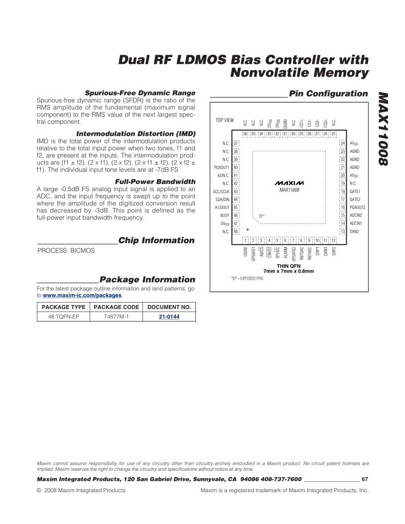
MA
X1
10
08
Dual RF LDMOS Bias Controller withNonvolatile Memory
Maxim cannot assume responsibility for use of any circuitry other than circuitry entirely embodied in a Maxim product. No circuit patent licenses areimplied. Maxim reserves the right to change the circuitry and specifications without notice at any time.
Maxim Integrated Products, 120 San Gabriel Drive, Sunnyvale, CA 94086 408-737-7600 ____________________ 67
© 2008 Maxim Integrated Products Maxim is a registered trademark of Maxim Integrated Products, Inc.
Spurious-Free Dynamic RangeSpurious-free dynamic range (SFDR) is the ratio of theRMS amplitude of the fundamental (maximum signalcomponent) to the RMS value of the next largest spec-tral component.
Intermodulation Distortion (IMD)IMD is the total power of the intermodulation productsrelative to the total input power when two tones, f1 andf2, are present at the inputs. The intermodulation prod-ucts are (f1 ± f2), (2 x f1), (2 x f2), (2 x f1 ± f2), (2 x f2 ±f1). The individual input tone levels are at -7dB FS.
Full-Power BandwidthA large -0.5dB FS analog input signal is applied to anADC, and the input frequency is swept up to the pointwhere the amplitude of the digitized conversion resulthas decreased by -3dB. This point is defined as thefull-power input bandwidth frequency.
Chip InformationPROCESS: BiCMOS
Package InformationFor the latest package outline information and land patterns, goto www.maxim-ic.com/packages.
PACKAGE TYPE PACKAGE CODE DOCUMENT NO.
48 TQFN-EP T4877M-1 21-0144
TOP VIEW
MAX11008
THIN QFN7mm x 7mm x 0.8mm
13
14
15
16
17
18
19
20
21
22
23
24
DXN2
ADCIN1
ADCIN2
PGAOUT2
GATE2
GATE1
N.C.
AVDD
AGND
AGND
AGND
AVDD
48
47
46
45
44
43
42
41
40
39
38
37
1 2 3 4 5 6 7 8 9 10 11 12
N.C.
DVDD
BUSY
A1/DOUT
SDA/DIN
SCL/SCLK
N.C.
A2/N.C.
PGAOUT1
N.C.
N.C.
N.C.
DXP2
DXN1
DXP1
REFA
DC
REFD
AC
OPSA
FE2
ALAR
M
SPI/I
2C
CNVS
T
A0/C
S
OPSA
FE1
DGND
36 35 34 33 32 31 30 29 28 27 26 25
N.C.
CS2+
CS2-
CS1-
CS1+
N.C.
DGND
DVDD
DVDD
N.C.
N.C.
N.C.
EP*
*EP = EXPOSED PAD.
+
Pin Configuration