
Development of a Nanoelectronic 3-D (NEMO 3-D ) Simulator for ...
35
Development of a Nanoelectronic 3-D (NEMO 3-D ) Simulator for Multimillion Atom Simulations and Its Application to Alloyed Quantum Dots Gerhard Klimeck, 1, * Fabiano Oyafuso, 1 Timothy B. Boykin, 2 R. Chris Bowen, 1 and Paul von Allmen 3 1 Jet Propulsion Laboratory, California Institute of Technology, Pasadena, CA 91109 2 Department of Electrical and Computer Engineering and LICOS, The University of Alabama in Huntsville, Huntsville, AL 35899 3 Motorola Labs, Solid State Research Center, 7700 S. River Pkwy., Tempe, AZ 85284 (Dated: May 2, 2002) Material layers with a thickness of a few nanometers are common-place in today’s semiconductor devices. Before long, device fabrication methods will reach a point at which the other two device dimensions are scaled down to few tens of nanometers. The total atom count in such deca-nano devices is reduced to a few million. Only a small finite number of “free” electrons will operate such nano-scale devices due to quantized electron energies and electron charge. This work demonstrates that the simulation of electronic structure and electron transport on these length scales must not only be fundamentally quantum mechanical, but it must also include the atomic granularity of the device. Various elements of the theoretical, numerical, and software foundation of the prototype development of a Nanoelectronic Modeling tool (NEMO 3-D ) which enables this class of device simulation on Beowulf cluster computers are presented. The electronic system is represented in a sparse complex Hamiltonian matrix of the order of hundreds of millions. A custom parallel matrix vector multiply algorithm that is coupled to a Lanczos and/or Rayleigh-Ritz eigenvalue solver has been developed. Benchmarks of the parallel electronic structure and the parallel strain calculation performed on various Beowulf cluster computers and a SGI Origin 2000 are presented. The Beowulf cluster benchmarks show that the competition for memory access on dual CPU PC boards renders the utility of one of the CPUs useless, if the memory usage per node is about 1-2 GB. A new strain treatment for the sp 3 s * and sp 3 d 5 s * tight-binding models is developed and parameterized for bulk material properties of GaAs and InAs. The utility of the new tool is demonstrated by an atomistic analysis of the effects of disorder in alloys. In particular bulk InxGa1-xAs and In0.6Ga0.4 As quantum dots are examined. The quantum dot simulations show that the random atom configurations in the alloy, without any size or shape variations can lead to optical transition energy variations of several meV. The electron and hole wave functions show significant spatial variations due to spatial disorder indicating variations in electron and hole localization. Keywords: quantum dot, alloy, nanoelectronic, sparse matrix-vector multiplication, tight-binding, optical transition, simulation. I. INTRODUCTION Ongoing miniaturization of semiconductor devices has given rise to a multitude of applications unfathomed a few decades ago. Although the reduction in minimum feature size of semiconductor devices has thus far ex- ceeded every expectation and overcome every predicted technological obstacle, it will nevertheless be ultimately limited by the atomic granularity of the underlying crys- talline lattice and the small number of “free” electrons. Before long, device fabrication methods will reach a point at which both quantum mechanical effects and effects induced by the atomistic granularity of the underlying medium (Fig. 1) need to be considered in the device de- sign. Quantum dots represent one incarnation of semicon- ductor devices at the end of the roadmap. Quantum dots can be characterized roughly as well-conducting, low energy regions surrounded on a nanometer scale by ”in- sulating” materials. The self-capacitance of the spatial confinement region is reduced with decreasing sizes. A situation can arise, in which the capacitive energy as- sociated with adding a single electron to the system is larger than the thermal energy, and charge quantiza- tion occurs. State quantization can occur if the cen- tral region is “clean” enough 103 and if the region’s di- mensions are roughly on the length scale of an electron wavelength. Quantum dot implementations in various material systems (including silicon) have been examined since the late 1980’s (Fig. 1b), and several designs have succeeded at room temperature operation. In particular pyramidal self-assembled quantum dot arrays appear to be promising candidates for use in quantum well lasers and detectors 1 within a few years. Although simulation has proven, especially in recent years, to be an important (and cost-effective) component of device design 4 , existing commercial device simulators typically ignore or “patch in” the quantum mechanical and atomistic effects that must be included in the next generation of electronic devices. This document describes the development of an atomistic simulation tool, NEMO- 3D, that incorporates quantum mechanical and atomistic effects by expanding the valence electron wave function in terms of a set of localized orbitals for each atom in
Transcript of Development of a Nanoelectronic 3-D (NEMO 3-D ) Simulator for ...

Development of a Nanoelectronic 3-D (NEMO 3-D ) Simulatorfor Multimillion Atom Simulations
and Its Application to Alloyed Quantum Dots
Gerhard Klimeck,1, ∗ Fabiano Oyafuso,1 Timothy B. Boykin,2 R. Chris Bowen,1 and Paul von Allmen3
1Jet Propulsion Laboratory, California Institute of Technology, Pasadena, CA 911092Department of Electrical and Computer Engineering and LICOS,The University of Alabama in Huntsville, Huntsville, AL 35899
3Motorola Labs, Solid State Research Center, 7700 S. River Pkwy., Tempe, AZ 85284(Dated: May 2, 2002)
Material layers with a thickness of a few nanometers are common-place in today’s semiconductordevices. Before long, device fabrication methods will reach a point at which the other two devicedimensions are scaled down to few tens of nanometers. The total atom count in such deca-nanodevices is reduced to a few million. Only a small finite number of “free” electrons will operate suchnano-scale devices due to quantized electron energies and electron charge. This work demonstratesthat the simulation of electronic structure and electron transport on these length scales must notonly be fundamentally quantum mechanical, but it must also include the atomic granularity of thedevice. Various elements of the theoretical, numerical, and software foundation of the prototypedevelopment of a Nanoelectronic Modeling tool (NEMO 3-D) which enables this class of devicesimulation on Beowulf cluster computers are presented. The electronic system is represented in asparse complex Hamiltonian matrix of the order of hundreds of millions. A custom parallel matrixvector multiply algorithm that is coupled to a Lanczos and/or Rayleigh-Ritz eigenvalue solver hasbeen developed. Benchmarks of the parallel electronic structure and the parallel strain calculationperformed on various Beowulf cluster computers and a SGI Origin 2000 are presented. The Beowulfcluster benchmarks show that the competition for memory access on dual CPU PC boards rendersthe utility of one of the CPUs useless, if the memory usage per node is about 1-2 GB. A newstrain treatment for the sp3s∗ and sp3d5s∗ tight-binding models is developed and parameterizedfor bulk material properties of GaAs and InAs. The utility of the new tool is demonstrated byan atomistic analysis of the effects of disorder in alloys. In particular bulk InxGa1−xAs andIn0.6Ga0.4As quantum dots are examined. The quantum dot simulations show that the randomatom configurations in the alloy, without any size or shape variations can lead to optical transitionenergy variations of several meV. The electron and hole wave functions show significant spatialvariations due to spatial disorder indicating variations in electron and hole localization.Keywords: quantum dot, alloy, nanoelectronic, sparse matrix-vector multiplication, tight-binding,optical transition, simulation.
I. INTRODUCTION
Ongoing miniaturization of semiconductor devices hasgiven rise to a multitude of applications unfathomed afew decades ago. Although the reduction in minimumfeature size of semiconductor devices has thus far ex-ceeded every expectation and overcome every predictedtechnological obstacle, it will nevertheless be ultimatelylimited by the atomic granularity of the underlying crys-talline lattice and the small number of “free” electrons.Before long, device fabrication methods will reach a pointat which both quantum mechanical effects and effectsinduced by the atomistic granularity of the underlyingmedium (Fig. 1) need to be considered in the device de-sign.
Quantum dots represent one incarnation of semicon-ductor devices at the end of the roadmap. Quantumdots can be characterized roughly as well-conducting, lowenergy regions surrounded on a nanometer scale by ”in-sulating” materials. The self-capacitance of the spatialconfinement region is reduced with decreasing sizes. Asituation can arise, in which the capacitive energy as-
sociated with adding a single electron to the system islarger than the thermal energy, and charge quantiza-tion occurs. State quantization can occur if the cen-tral region is “clean” enough103 and if the region’s di-mensions are roughly on the length scale of an electronwavelength. Quantum dot implementations in variousmaterial systems (including silicon) have been examinedsince the late 1980’s (Fig. 1b), and several designs havesucceeded at room temperature operation. In particularpyramidal self-assembled quantum dot arrays appear tobe promising candidates for use in quantum well lasersand detectors1 within a few years.
Although simulation has proven, especially in recentyears, to be an important (and cost-effective) componentof device design4, existing commercial device simulatorstypically ignore or “patch in” the quantum mechanicaland atomistic effects that must be included in the nextgeneration of electronic devices. This document describesthe development of an atomistic simulation tool, NEMO-3D, that incorporates quantum mechanical and atomisticeffects by expanding the valence electron wave functionin terms of a set of localized orbitals for each atom in
2
����� �
����� �
����� �
�����
����� ����������������������������� ��� ��� ��� ���� � �! "�#
$&%�'&(
)+* ,.-0/ '�1&23'&4
576983:
;=<&>�?�@A<�BC5ED�F�G H�D�IJKI�G ?�L�M DND�M D�HO@AP QR?�G H�I�JJKI�S�G ?�@ P Q�?�G HI�J
TU:=VXW5ED�F�G H�DRI
TU:=VYWZ5[D�F�G HD�I\ G @ ]^;=<�>R?�@ <�B._�` ` D�HO@ I
���Ra
���0b
���Rc
���Rd
����e
�����f����g������g�����h�g������
i ��j ��kl mn �o� �k�p
$&%�'&(
qEr sut&v wyx z&{O| } wR~� w�vRq��0s7�
�[��2X�O%�( /O�U��� %��h� ( /&�O�
���0�������R��� ������������� �0��������A��� ��� �N���0� �������K����� �R ¡�
¢¤£ ¥§¦h¨ ©¤ª¤«¬��« ¯® ª¤°K« ® ±�²A« ¨
³ '�´ ³ �´
hµ ¯²A« ® ¶ ²K·hµ µ ¸¹ ·�« º©�¦h¨ ©¤ª¤« °
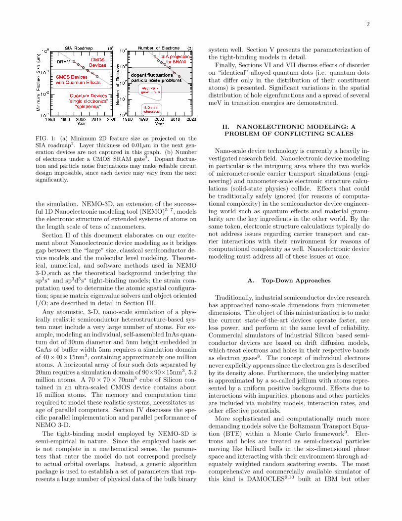
FIG. 1: (a) Minimum 2D feature size as projected on theSIA roadmap2. Layer thickness od 0.01µm in the next gen-eration devices are not captured in this graph. (b) Numberof electrons under a CMOS SRAM gate3. Dopant fluctua-tion and particle noise fluctuations may make reliable circuitdesign impossible, since each device may vary from the nextsignificantly.
the simulation. NEMO-3D, an extension of the success-ful 1D Nanoelectronic modeling tool (NEMO)5–7, modelsthe electronic structure of extended systems of atoms onthe length scale of tens of nanometers.
Section II of this document elaborates on our excite-ment about Nanoelectronic device modeling as it bridgesgap between the “large” size, classical semiconductor de-vice models and the molecular level modeling. Theoret-ical, numerical, and software methods used in NEMO3-D ,such as the theoretical background underlying thesp3s∗ and sp3d5s∗ tight-binding models; the strain com-putation used to determine the atomic spatial configura-tion; sparse matrix eigenvalue solvers and object orientedI/O; are described in detail in Section III.
Any atomistic, 3-D, nano-scale simulation of a phys-ically realistic semiconductor heterostructure-based sys-tem must include a very large number of atoms. For ex-ample, modeling an individual, self-assembled InAs quan-tum dot of 30nm diameter and 5nm height embedded inGaAs of buffer width 5nm requires a simulation domainof 40×40×15nm3, containing approximately one millionatoms. A horizontal array of four such dots separated by20nm requires a simulation domain of 90×90×15nm3, 5.2million atoms. A 70 × 70 × 70nm3 cube of Silicon con-tained in an ultra-scaled CMOS device contains about15 million atoms. The memory and computation timerequired to model these realistic systems, necessitates us-age of parallel computers. Section IV discusses the spe-cific parallel implementation and parallel performance ofNEMO 3-D.
The tight-binding model employed by NEMO-3D issemi-empirical in nature. Since the employed basis setis not complete in a mathematical sense, the parame-ters that enter the model do not correspond preciselyto actual orbital overlaps. Instead, a genetic algorithmpackage is used to establish a set of parameters that rep-resents a large number of physical data of the bulk binary
system well. Section V presents the parameterization ofthe tight-binding models in detail.
Finally, Sections VI and VII discuss effects of disorderon “identical” alloyed quantum dots (i.e. quantum dotsthat differ only in the distribution of their constituentatoms) is presented. Significant variations in the spatialdistribution of hole eigenfunctions and a spread of severalmeV in transition energies are demonstrated.
II. NANOELECTRONIC MODELING: A
PROBLEM OF CONFLICTING SCALES
Nano-scale device technology is currently a heavily in-vestigated research field. Nanoelectronic device modelingin particular is the intriguing area where the two worldsof micrometer-scale carrier transport simulations (engi-neering) and nanometer-scale electronic structure calcu-lations (solid-state physics) collide. Effects that couldbe traditionally safely ignored (for reasons of computa-tional complexity) in the semiconductor device engineer-ing world such as quantum effects and material granu-larity are the key ingredients in the other world. By thesame token, electronic structure calculations typically donot address issues regarding carrier transport and car-rier interactions with their environment for reasons ofcomputational complexity as well. Nanoelectronic devicemodeling must address all of these issues at once.
A. Top-Down Approaches
Traditionally, industrial semiconductor device researchhas approached nano-scale dimensions from micrometerdimensions. The object of this miniaturization is to makethe current state-of-the-art devices operate faster, useless power, and perform at the same level of reliability.Commercial simulators of industrial Silicon based semi-conductor devices are based on drift diffusion models,which treat electrons and holes in their respective bandsas electron gases8. The concept of individual electronsnever explicitly appears since the electron gas is describedby its density alone. Furthermore, the underlying matteris approximated by a so-called jellium with atoms repre-sented by a uniform positive background. Effects due tointeractions with impurities, phonons and other particlesare included via mobility models, interaction rates, andother effective potentials.
More sophisticated and computationally much moredemanding models solve the Boltzmann Transport Equa-tion (BTE) within a Monte Carlo framework9. Elec-trons and holes are treated as semi-classical particlesmoving like billiard balls in the six-dimensional phasespace and interacting with their environment through ad-equately weighted random scattering events. The mostcomprehensive and commercially available simulator ofthis kind is DAMOCLES9,10 built at IBM but other

3
BTE based simulators have also recently appeared onthe market11,12.
The hydrodynamic approximation to the BTE has re-cently given rise to a class of models that is a step be-tween the drift diffusion approach and the full-fledgedBTE solver. Whereas the drift diffusion approach es-sentially only considers the zeroth order moment of theBTE, the hydrodynamic model extends the approxima-tion to the first and second order moments. This treat-ment of higher order moments yields familiar momentumand energy conservation equations for an ideal fluid withadditional terms for the electric and possibly the mag-netic field. The hydrodynamic method enjoys consider-able popularity since it describes hot carrier transportbetter than drift diffusion models yet it is significantlyfaster than the Monte Carlo BTE method.
An industry has evolved dedicated to the develop-ment and maintenance of such semiconductor devicesimulators8,12,13. However, quantum mechanical effectssuch as tunneling and state quantization are not explic-itly included in these models. Current efforts in the tra-ditional device simulation community mainly focus onincluding these quantum mechanical effects into exist-ing device simulation models incurring the least possiblecomputational expense and with the overriding require-ment of preserving the overall framework of the existingsimulation tools. However, the problem with such simu-lator extensions is that they depend heavily on empiricalparameterization to operate well on existing devices. Theuse of these tools and its parameterizations is generallynot accurate for the next generation of devices.
B. Bottom-up Approaches
While the industry oriented semiconductor device re-search community approaches nano-scale transport fromthe top down, the physics oriented solid state researchcommunity approaches the same regime from the bottomup. The models in the latter approach are fully quantummechanical and can only be applied to relatively smallsystems with emphasis on high accuracy. The systemsare often periodic with unit cells containing a few hun-dred to a few thousand atoms, and the main output is theelectronic structure and the equilibrium atomic configu-ration with emphasis on surface and interface reconstruc-tion and on impurity and defect levels. Charge transportis usually not included at the fundamental level, althoughsome attempts are mentioned below.
In contrast to the methods discussed in Section II A,electronic structure calculations explicitly include thegranularity of condensed matter and describe the atomsat various levels of sophistication. At a fundamen-tal level, the electrons are described by a many bodySchrodinger equation in which the Hamiltonian containsinteraction potentials with the atoms as well as electron-electron interaction terms. In this approach, it has al-
ready been assumed that the electrons adiabatically fol-low the motion of the atoms. Effects beyond this approx-imation lead to electron-phonon interaction terms thatare evaluated in subsequent steps. In most cases, eventhe full electron problem is intractable, and calculationsinvolving more than a handful of atoms rely on the so-called single electron approximation. The single electronapproximation circumvents the difficulties raised by theinteraction between the electrons by introducing a localor sometimes a non-local potential into a one particleSchrodinger equation. Familiar implementations of thisidea are the Hartree-Fock approximation14 and densityfunctional theory15–17. Alternate approaches using thefull Hamiltonian that explicitly includes electron-electroninteraction are based on methods such as quantum MonteCarlo18.
Within the one-electron picture, it is in some casespossible to solve the all-electron problem, which meansthat all the electrons in the atoms are explicitly includedin the self-consistent solution of the density dependentSchrodinger equation. The atom is then simply describedby a Coulomb potential with the appropriate charge forthe nucleus. However, in most situations only a restrictednumber of electrons in the atom participate in the chemi-cal bonding and transport properties (valence electrons).Several methods have emerged where the core electronsare taken into account by modifying the Coulomb poten-tial of the nucleus with an additional repulsive potential,which describes the interaction of the core electrons withthe valence electrons. The resulting potential is termed“pseudopotential”. A number of approaches that havebeen explored to build these crucial components of elec-tronic structure calculations are described below.
Pseudopotentials are divided into several classes. Em-pirical pseudopotentials are fitted so that a set of calcu-lated properties match experimental results. Such em-pirical pseudopotentials can be defined in real space by aparameterized function or directly in reciprocal space,which offers advantages for periodic systems and wasone of the first avenues explored19. The real spacepseudopotentials20,21 offer the advantage that non-bulksystems such as interfaces and surfaces can be describedmore realistically.
First principles pseudopotentials do not require any fit-ting procedure, but they do require the knowledge of theeigenstates and eigenenergies for isolated atoms. A num-ber of schemes have been devised, most of which strive toeliminate the nodes in the valence band electronic wavefunctions within the core region, to reduce the computa-tional cost of the numerical solutions. These schemes, inturn, can be divided into two categories.
Norm conserving pseudopotentials are derived(through inversion of the Schrodinger equation) frompseudo-wave functions with the reassuring propertythat the associated integrated charge inside the coreregion is identical to the charge obtained with the exacteigenfunctions. The most famous example and the most

4
widely used for benchmarks is the method by Bachelet,Hamann and Schluter22. Another method that hasgained considerable popularity in conjunction with aplane wave expansion for the numerical solution waslater developed by Troullier and Martins23. Troullierand Martins method differs by the prescription used tobuild the pseudo wave functions
Norm-conserving pseudopotentials require a largeplane wave cutoff for elements of the first row, oxygen,and a number of other elements because the pseudo-wavefunction cannot be made sufficiently smooth in thecore region. Conversely, a real space method wouldrequire a very fine mesh. Vanderbilt24 recently intro-duced a successful ultra-soft pseudopotential for whichthe norm-conserving constraint is relaxed. The disadvan-tages of Vanderbilt’s method are more complex codingand the need to solve a generalized eigenvalue problem,rather than a standard eigenvalue problem.
While this document has reviewed the description ofatoms with pseudopotentials it should be mentioned thata number of important issues related to improvements tothe density functional theory and to the development ofefficient numerical methods, which both lay at the core ofother current investigations in the field, have been omit-ted.
Finally, as already mentioned, although earlier mostelectronic structure calculations using pseudopotentialsare restricted to systems much smaller than the quantumdots of interest in this work, it is worthwhile noting that,with a number of approximations, Zunger25 et al. haverecently managed to extend some of their pseudopoten-tial work to systems containing up to one million atoms.Zunger’s method has been applied extensively (see forexample [26,27]) to model quantum dot structures, how-ever, without yet including transport calculations.
C. An Intermediary Approach
Whereas traditional semiconductor device simulatorsare insufficiently equipped to describe quantum effectsat atomic dimensions, most ab-initio methods from con-densed matter physics are still computationally too de-manding for application to practical devices, even assmall as quantum dots. A number of intermediary meth-ods have therefore been developed in recent years. Themethods can be divided into two major theory categories:atomistic and non-atomistic.
The non-atomistic approaches do not attempt to modeleach individual atom in the structure, but introduce a va-riety of different approximations that are usually basedon a continuous, jellium-type description of matter. Atthe lowest order approximation, such approaches only re-tain effective masses and band edges from the full elec-tronic band structure, and they have given rise to thewell-known effective mass approximation, in which onthe scale of atomic distances a slowly varying envelope
function describes the carriers. That envelope function isthe solution to a one-particle effective mass Schrodingerequation. The general k ·p method leads to a straight-forward extension of that approximation by includingthe coupling between multiple bands. The k ·p methodhas given rise to the popular multi-band effective massapproximation28,29, in which an envelope function is as-sociated with each band explicitly included in the calcu-lation, and a set of coupled Schrodinger-like equationsis solved. It should be noted that the limitation toslowly varying perturbations remains in the multi-bandversion30. The different materials are described by space-dependent parameters which are separately determinedfor each of the materials in the device.
One strength of the effective mass approximation is thecapability to discretize realistically-sized systems with-out the tremendous computational expense of previouslymentioned ab-initio methods. However, the approxima-tion inherently does not contain any direct atomic levelinformation, and is, therefore, not well suited for therepresentation of nano-scale features such as interfacesand disorder from a fundamental perspective. This lim-itation has sparked lively discussions concerning the va-lidity of the near-zone center plane wave expansion k ·pbasis and the need to include each atom in the simula-tion31–33. Despite its limitations the effective mass ap-proximation has provided excellent agreement with mea-surements for a large number of experiments. Anotherinteresting issue34,35 of particular relevance to quantumdots relates to the most appropriate treatment of strain:should continuum or atomistic models be preferred? Thiswork uses the atomistic valence force field method byKeating34.
Atomistic approaches attempt to work directly withthe electronic wave function of each individual atom. Ab-initio methods overcome the shortcomings of the effectivemass approximation, however, additional approximationsmust be introduced to reduce computational costs. Asdescribed briefly in the previous section, one of the criti-cal questions is the choice of a basis set for the represen-tation of the electronic wave function. Many approacheshave been considered, ranging from traditional numericalmethods, such as finite difference and finite elements, aswell as plane wave expansions25, to methods that exploitthe natural properties of chemical bonding in condensedmatter. Among these latter approaches, local orbitalmethods are particularly attractive. While the method ofusing atomic orbitals as a basis set has a long history insolid state physics, new basis sets with compact supporthave recently been developed36, and, together with spe-cific energy minimization schemes, these new basis setsresult in computational costs which increase linearly withthe number of atoms in the system without much accu-racy degradation37,38. However, even with such methods,only a few thousand atoms can be described with presentday computational resources. NEMO 3-D uses an empiri-cal tight-binding method39,40 that is conceptually related

5
to the local orbital method and that combines the ad-vantages of an atomic level description with the intrinsicaccuracy of empirical methods. It has already demon-strated considerable success5–7 in quantum mechanicalmodeling of electron transport as well as the electronicstructure modeling of small quantum dots41.
The underlying idea of the empirical tight-bindingmethod is the selection of a basis consisting of atomicorbitals (such as s, p, and d) which create a sin-gle electron Hamiltonian that represents the bulk elec-tronic properties of the material. Interactions be-tween different orbitals within an atom and betweennearest neighbor atoms are treated as empirical fittingparameters. A variety of parameterizations of near-est neighbor and second-nearest neighbor tight-bindingmodels have been published, including different orbitalconfigurations39,40,42–46. NEMO 3-D typically uses ansp3s∗ or sp3d5s∗ model that consists of five or ten spindegenerate basis states, respectively.
For the modeling of quantum dots, three mainmethods have been used in recent years: k · p47,48,pseudopotentials25, and empirical tight-binding41. It isfair to note that each of these methods grapples with thesame intrinsic difficulty: the full description of about amillion interacting atoms and all of their electrons. Itshould also be emphasized that for most semiconductorcompounds, only fragmentary experimental data existsfor the band gaps and effective masses and their depen-dence on stress and strain. While ab-initio pseudopo-tential calculations beyond density functional theory doin principle predict such properties, the computationalcost is high for even simple properties such as the elec-tronic band gap49. It should also be noted that effectivemasses, which are a crucial element in the determina-tion of correct electronic state quantization, are rarelylisted as a result of first principles calculations. On theother hand, more empirical approaches such as k ·p andtight-binding use “quality” bulk parameterizations andcan achieve good experimental comparisons in quantumdot simulations. The question, however, remains whetherthese parameterizations are valid in presence of varia-tions at the atomic scale. These on-going efforts can beviewed as complementary rather than mutually exclusivecompetitors, and each method can greatly benefit frominsightful cross-fertilization.
The perspective taken in this work is that empiricaltight-binding models link the physical content of theatomic level wave functions of the pseudopotential cal-culations to the jellium approach of k · p, and are themethod of choice for realistic modeling of transport inquantum dot structures. Finally, as will be discussed infurther detail, it should be emphasized that the qualityof the empirical tight-binding results depends strongly ona good parameterization of the bulk material properties.
D. Nanoelectronics with Transport
Nanoelectronic device simulation must ultimately in-clude both, the sophisticated physics oriented electronicstructure calculations and the engineering oriented trans-port simulations. Extensive scientific arguments have re-cently ensued regarding transport theory, basis represen-tation, and practical implementation of a simulator ca-pable describing a realistic device.
Starting from the field of molecular chemistry, Rat-ner et al applied50 tight-binding based approaches to themodeling of transport in molecular wires. Later, Derosaand Seminario51 modeled molecular charge transport us-ing density functional theory and Green functions. Fur-ther significant advances in the understanding of the elec-tronic structure in technologically relevant devices wererecently achieved through ab initio simulation of MOSdevices by Demkov and Sankey52. Ballistic transportthrough a thin dielectric barrier was evaluated using stan-dard Green function techniques53,54 without scatteringmechanisms.
Conversely, starting from the field of semiconductor de-vice simulation, various efforts have been undertaken overthe past eight years to develop quantum mechanics-baseddevice simulators that incorporate scattering mechanismsat a fundamental level. The Nanoelectronic Modelingtool (NEMO 1-D ) built at Texas Instruments / Raytheonfrom 1993-1997 is possibly the first large-scale device sim-ulator based on the non-equilibrium Green function tech-nique (NEGF) to meet the challenge. Its initial objectivewas to achieve a comprehensive simulation of the electrontransport in resonant tunneling diodes (RTDs). NEGF isa powerful formalism capable of combining tight-bindingband structure, self-consistent charging effects, electron-phonon interactions, and disorder effects with the impor-tant concept of charge transport from one electron reser-voir to another. The concept of electron transport be-tween reservoirs was pioneered in a simpler approach byLandauer and Buttiker55,56, and later expanded for theNEGF formalism by Caroli57 et al. Tunneling throughsilicon dioxide barriers, which is a classical problem ofgreat technological interest for the development of thindielectrics, was studied using tight-binding models withinNEMO7 as well as in a large 3-D cell model by Stadele58.Other research groups59–62 have since then started to de-velop NEGF-based simulators to model MOSFET de-vices in a 2-D simulation domain. These simulationsare computationally extremely intensive, and fully ex-ploit the computing power of realistically available par-allel supercomputers and cluster computers.
Quantum mechanical simulations of electron transportthrough 3-D confined structures such as quantum dotshave not yet reached the maturity of the 1-D and 2-D sim-ulation capabilities mentioned above. Early efforts wererate equation based63–65, where a simplified electronicstructure was assumed. In the related area of molecu-lar structures, detailed studies of charge transport have

6
recently become a hot research topic where simulationsare providing an improved understanding of experimen-tal data66,67.
NEMO 3-D focuses on the atomistic electronic struc-ture calculation of realistically sized quantum dots at thisdevelopment stage. This work is a complement to quan-tum dot simulations26,27,47,48,68,69 performed with othermethods discussed in this section. NEMO 3-D currentlydoes not include carrier transport. However, the Lanczosalgorithm (see Section III F) has been tested successfullyalready for non-Hermitian matrices, introduced by openboundary conditions (see Section III C) and the code isstructured such that transport simulations can be incor-porated in the future without major re-writes of the soft-ware.
III. THEORETICAL, NUMERICAL, AND
SOFTWARE METHODS
A. Tight Binding Formulation Without Strain
Quantum dots are characterized by confinement inall three spatial dimensions so that the Hamiltonian nolonger commutes with any of the discrete translation op-erators. The wave vector is hence not a good quantumnumber in any direction. The most natural basis for rep-resenting such a highly confined wave function is, there-fore, one consisting of atomic-like orbitals centered oneach atom of the crystal. Solving for the electronic struc-ture of a quantum dot requires detailed modeling of thelocal environment on an atomic scale, and, therefore, in-troduces material considerations into the calculation.
While quantum dots may be fabricated in any num-ber of materials systems, from an electronic struc-ture point of view, the treatment employed mainlydepends on whether the bulk lattice constants of allmaterials are the same. When the bulk lattice con-stants are the same the system is said to be lattice-
matched; when they are not, the system is said tobe lattice-mismatched. Lattice-matched examples in-clude GaAs/AlAs and its alloys GaxAl1−xAs, as wellas In0.53Ga0.47As/In0.52Al0.47As. An InAs quantum dotsurrounded by AlxGa1−xAs and an InAs or AlAs layerin a high performance In0.53Ga0.47As/InP resonant tun-neling diode are examples of lattice-mismatched devices.The treatment of the two cases is necessarily somewhatdifferent, since a matrix element of the Hamiltonian be-tween two orbitals centered on different atoms depends,in general, on the position of the atoms. In this workthe two-center approximation is made, so that only therelative position of neighboring atoms is important. Ina lattice-matched system, the atoms constitute a perfectcrystal with uniform unit cells; in a lattice-mismatchedsystem, the atomic positions vary and are only semi regu-lar. In other words, in such a system one can roughly dis-cern unit cells, but these cells vary somewhat in size, andthe atomic positions within them vary. The Keating34
valence force field model described later is employed inNEMO 3-D to determine the atomic positions.
For both types of materials systems, the atomic-likeorbitals are assumed to be orthonormal, following Slaterand Koster70. Bravais lattice points can describe a crys-tal in a lattice-matched system:
Rn1,n2,n3 = n1a1 + n2a2 + n3a3 (1)
where ai are primitive direct lattice translation vectorsand ni are integers. If there is more than one atom percell, as is the case with, for example, GaAs or Si, theatoms within a cell are indexed by µ, and the locationof the µth atom within the cell located at Eq.(1) is givenby Rn1,n2,n3 + vµ, where vµ is the displacement relativeto the cell origin. The wavefunction is normalized over avolume consisting of Ni cells in the ai (i = 1, 2, 3) direc-tion, and the state is represented as a general expansionin terms of localized atomic-like orbitals:
|Ψ> =1√
N1N2N3
N1∑
n1=1
N2∑
n2=1
N3∑
n3=1
∑
α
∑
µ
C(αµ)n1n2n3
|αµ;Rn1,n2,n3 + vµ> (2)
In Eq.(2), α indexes the atomic-like orbitals centered on the µ atoms within each cell (n1, n2, n3). The Schrodingerequation thus appears as a system of simultaneous equations given by:
<αµ;Rn1,n2,n3 + vµ|H −E|Ψ> = 0 (3)
In Eq.(3) the matrix elements between localized orbitalsare expressed as tight-binding parameters with the addi-tional limitation of interactions to nearest neighbors. Thesp3s∗ model of Vogl39 et al, as well as the sp3d5s∗ model
of Jancu et. al.40, are employed within the two-center ap-proximation, in which the matrix elements depend onlyupon the relative positions of the orbitals. The expres-sions for the matrix elements between these types of or-

7
bitals in the two-center approximation are given by Slaterand Koster70 as functions of the relative atomic positions.
B. Tight Binding Formulation With Strain
In a lattice-mismatched system several additional com-plications arise. First, the “cells” are no longer regularlyplaced so that the Rn1,n2,n3 are no longer representablein a form given by Eq.(1). In a lattice-mismatched quan-tum dot fabricated from zincblende crystal materials, theRn1,n2,n3 are best considered as giving the location of ananion-cation pair. Likewise, in Eq.(3), the displacementsnow depend on both the specific “cell” and atom type,and are more correctly written as vn1n2n3
µ . These com-plications, though important, are rather minor and areautomatically accommodated since there is no assump-tion of a wave-vector in any dimension in Eq.(2).
The second complication affects the nearest neighborparameters. As mentioned above, in the two-center ap-proximation these nearest neighbor parameters dependupon the relative atomic positions. For example, theHamiltonian matrix element between an s-orbital cen-tered about an atom at the origin and a px-orbital cen-tered about an atom located at d = `x+my+nz, whered is the distance between the atoms and `, m, and n arethe direction cosines is:
Esx = `Vspσ (4)
Since the bond angle between atoms is no longer uniformin a lattice-mismatched system, the direction cosinesvary in magnitude for different pairs of nearest neighboratoms, even in nominally zincblende or diamond struc-ture materials. Furthermore, the two-center parameterssuch as Vspσ no longer take on their ideal values as dis-tance d between the atoms in each pair is in general dif-ferent from its ideal (bulk crystal) value. The two-centerparameters are assumed to scale as:
Vαβγ =(d0
d
)ηαβγ
V(0)αβγ (5)
where for the given pair of atoms d0 is the ideal sepa-
ration, d is the actual separation, and V(0)αβγ is the ideal
parameter for the orbitals involved. The exponents arechosen to reproduce known bulk behavior under condi-tions such as hydrostatic pressure. From the work ofHarrison71, it is expected that most of these exponentsshould be approximately 2.
Also the same-site parameters are, generally, changedfrom their bulk values. In a lattice-matched system, how-ever, the changes are usually small. In the sp3d5s∗ model,there may be no change at all, since in this model it isoften possible to use a single set of onsite parameters fora given atom type, independent of the material. For ex-ample, As has the same parameters in GaAs, AlAs, andInAs (see Table III).
In a lattice-mismatched system, atom displacementsaffect the same-site parameters more strongly. To un-derstand the reason for this shift, recall that the atomic-like orbitals are assumed to be orthogonal. They are,thus, not true atomic orbitals, but are more properlyLowdin functions72, which are orthogonal yet transformunder symmetry operations of the crystal, as would theatomic orbital whose label they bear. When atoms aredisplaced in a lattice-mismatched system, not only do thetight-binding parameters of Eq.(4) change, so, too, dothe overlaps of the true atomic orbitals from which theLowdin functions are constructed. While the overlapsdo not appear in an orthogonal, empirical tight-bindingapproach such as the one employed here, a reasonable ap-proximation is to assume that the overlap between twonearest neighbor orbitals is proportional to their Hamil-tonian matrix element divided by the sum of the vacuum-referenced onsite energies of the orbitals71. With this ap-proximation Lowdin’s formula is used to first order in theorbital overlaps to obtain an onsite Hamiltonian matrixelement, which includes the effect of the displacement ofthe nearest neighbor atoms:
Eiα ≈ E(0)iα +
∑
jβ
Ciα,jβ
(
E(0)(iα,jβ)
)2
−(
E(iα,jβ)
)2
E(0)iα + E
(0)jβ
(6)
where E(0)iα is the vacuum-referenced ideal same-site
Lowdin orbital parameter for an α-orbital on theith atom, Eiα is the shifted vacuum-referenced corre-
sponding same-site Lowdin orbital parameter, E(0)(iα,jβ)
(
E(iα,jβ)
)
the ideal (lattice-mismatched) nearest neigh-
bor parameter between an α-orbital on the ith atom anda β-orbital on the j th atom, and Ci,α,jβ is a propor-tionality constant fit to properly reproduce bulk strainbehavior. The sum covers all orbitals β and atoms j thatare nearest neighbors of the atom i. The difference insquared matrix elements effectively removes the onsiteshift implicit in the ideal onsite parameter, and replacesit with the lattice-mismatched shift. Parameterizationsof InAs and GaAs, including the strain-induced shift ofthe on-site elements, are discussed in Section V B.
C. Electronic Structure Boundary Conditions
The finite simulation domain that is represented in theelectronic structure calculation as a sparse matrix mustbe terminated by physically meaningful boundary condi-tions. There are currently 2 kinds of boundary conditionsimplemented in NEMO 3-D: periodic and closed system.Periodic boundary conditions which satisfy Bloch’s the-orem allow for a study of the bulk properties of alloysas long as the periodicity of the domain is much largerthan the largest feature size within the domain. Closedsystem boundary conditions terminate the bonds of the
8
surface atoms abruptly. The dangling bonds are “pas-sivated” with fixed potentials to avoid the inclusion ofsurface states in the energy range of interest. The thick-ness of an isolating GaAs buffer around a InAs quantumdot does influence the energy of the confined states, andthe buffer size must be chosen adequately large.
Another desirable boundary condition developed in theNEMO 1-D code is the open boundary through whichparticles can be injected from reservoirs and throughwhich particles can escape to reservoirs. The bound-ary conditions developed73,74 for NEMO 1-D were thekey to the success in the transport simulations throughrealistically sized resonant tunneling diodes5,6 and MOSdevices7. These boundary conditions change the charac-ter of the Hamiltonian matrix from Hermitian to non-Hermitian, and the imaginary part of the quasi-boundstate eigen-energies now corresponds to the lifetime ofthe state in the confinement. To enable the simulation
of charge transport in NEMO 3-D , an open boundarycondition for the 3-D system is currently under develop-ment.
D. Atomistic Strain Calculation
An accurate calculation of the electronic structurewithin the tight-binding model necessitates an accuraterepresentation of the positions of each atom. The atompositions in strained materials are shifted from the idealbulk positions to minimize the overall strain energy ofthe system. NEMO 3-D uses a valence force field (VFF)model34,35 in which the total strain energy, expressed asa local nearest neighbor functional of atomic positions,is minimized. The local strain energy at atom i is givenby:
Ei =3
16
∑
j
[ αij
2d2ij
·(
R2ij − d2
ij
)2
+n
∑
k>j
√
βijβik
dijdik
(
Rij ·Rik − dij · dik
)2]
(7)
where the sum is over neighbors j of atom i. Here, dij
and Rij are the equilibrium and actual distances betweenatoms i and j, respectively. Eq. 7 is included as Eq. 14in reference [35] except for some corrected coefficients.The local parameters αij and βij represent the force con-stants for bond-length and bond-angle distortions in bulkzinc-blende materials, respectively, and, in the absence ofCoulomb corrections, are related to the bulk elastic mod-uli by:
C11 + 2C12 =
√3
4dij
(
3αij + βij
)
(8)
C11 − C12 =
√3
dijβij
C44 =
√3
4dij
4αijβij
αij + βij
In zinc-blende materials, however, these relations aremodified by the inclusion of Coulomb effects due to theunequal charge distribution between the anion and cationsublattices. In this paper, α’s and β’s obtained by Martinto account for the Coulomb correction75 are used. Thetotal strain energy is computed as the sum of the localstrain energies over all atoms.
E. Atomistic Strain Boundary Conditions
Several boundary conditions for the strain calculationare currently implemented in NEMO 3-D . To model
systems of finite extent, three boundary conditions areavailable: 1) the hard wall condition in which all outershell atoms are fixed to user determined lattice constants,2) the soft wall condition in which no atom position isfixed, and 3) the softwall boundary condition in whichone atom position in the system is fixed.
To enable the simulation of bulk systems, periodicboundary conditions have been implemented. In thiscase the dimensions of the fundamental domain and,therefore, the separations between neighboring bound-ary atoms are not known a priori. Thus, the crystal isallowed to “breathe” such that the strain energy is alsominimized with respect to the period in each direction inwhich periodic boundary conditions are applied.
F. Eigenvalue Solution
One simulation objective is to solve the eigenvalueproblem for low lying electron and hole states near thebandedge. The nearest neighbor tight-binding Hamil-tonian can be represented in a sparse matrix. A onemillion atom system represented in the sp3d5s∗ basis es-tablishes a matrix size of 20 million× 20 million. A “di-rect solver”, in which the entire column space is workedon is completely unfeasible for a variety of reasons, es-pecially due to the full matrix storage requirement of(20×106)2×16 bytes=6400TB. A variety of sparse ma-trix eigenvalue and eigenvector algorithms have been de-veloped, some of which are available publicly76. Most

9
of these eigenvalue/vector algorithms are some form ofa Krylov/Lanczos/Arnoldi subspace approach77. Thesemethods approximate the solution on a small subspacewhich is increased until a desired tolerance is achieved.One the major advantage is that only require memory ofthe order of the length of several eigenvectors is required.At the lowest level of the algorithm, trial vectors are re-peatedly multiplied by the matrix of interest. Storageof the matrix is not mandatory if the matrix can be re-constructed on the fly during the matrix-vector multiplyprocess. The performance of these algorithms operat-ing on large systems, therefore, strongly depends on theefficient implementation of a matrix-vector multiply al-gorithm for the problem at hand.
The Lanczos-based solver technology78 of non-Hermitian matrices developed78 for NEMO 1-D was ap-plied for NEMO 3-D as well. Early in the developmentof NEMO 3-D, the Lanczos-eigenvalue solver prototypewith was compared ARPACK76. For a system of about100,000 atoms it was found that our custom solver wassignificantly faster104 than ARPACK. Therefore, paral-lelization of our custom solver was implemented to attacklarge-scale problems.
The folded-spectrum method79, which is based on aminimization of the squared target matrix, has been pro-posed, implemented, and heavily used by Zunger et al.Before the matrix is squared it is shifted to the energyrange of interest, i.e. close to the expected eigenenergies.The overall algorithm is then based on a conjugate gra-dient minimization of a trial vector. This method alsorelies heavily on a matrix-vector multiply algorithm andit has been implemented in NEMO 3-D.
G. Software Methods
The NEMO 3-D project leverages some of the soft-ware technology developed in the original NEMO 1-D project80,81 as well as improvements of NEMO 1-Dundertaken at JPL82,83. NEMO 1-D contains roughly250,000 lines of C, FORTRAN and F90 code. Data man-agement is performed in an object oriented fashion in C,without using C++. On the lowest level, FORTRAN andF90 are used to perform small matrix operations such asmatrix inversions and matrix-vector multiplication. Thelanguage hybrid structure was introduced to utilize fastFORTRAN and F90 compilers that were available on theSGI, HP, and Sun development machines in the earlystages of NEMO 1-D. At that time identical algorithmswritten in FORTRAN and C showed that FORTRANcould outperform C by about a factor of 4. On today’sIntel cluster based computers such a speed discrepancymay not really exist anymore in part due to the advance-ments in C compilers and the lack of competition for fastFORTRAN compilers.
One major software component in NEMO 1-D is therepresentation of materials in a tight-binding basis in-
cluding various orbitals and nearest neighbor counts.Adding a new tight-binding model amounts to adding anew Hamiltonian constructor. Bulk band structure andcharge transport calculations are almost independent ofthe underlying Hamiltonian details and form a higherlevel building block by themselves. This modular designenables the introduction of more advanced tight-bindingmodels as they become available, without interfering withhigher level algorithms. The sp3d5s∗ model has beenadded at JPL recently within this architecture.
A hierarchically higher software block in NEMO 1-D accesses the bulk bandstructure routines through ascript-based database module. The ASCII database canbe modified outside the NEMO 1-D core to contain ar-bitrary tight-binding input parameters as well as a va-riety of different database entries. The relatively sim-ple database access to bulk bandstructure has enableda straight-forward integration of NEMO into a geneticalgorithm based optimization tool. This tool is usedfor tight-binding parameter optimization as discussed onSection V A. The material parameter database is alsoaccessed in the new NEMO 3-D code.
Most research oriented simulators must be fed a washlist of parameters, some of which are dependent on oth-ers, some of which may be superfluous, or some of whichmay cause crashes unless some other options have beenset. Often these dependencies require an expert userincreasing the initial barrier to simulator usage. TheNEMO 1-D input has been structured hierarchically suchthat the user can provide information in automated de-pendent blocks. Information is, therefore, requested fromthe user as a progressively dependent input. Such inputpresentation is customary in a properly implemented ina graphical user interface (GUI).
Such well organized user input presentation is rela-tively simply incorporated with a static GUI in softwarewhose input is well specified. Research software underrapid development, however, tends to change its require-ments frequently. Rapid changes force a static GUI toalways lag behind the actual theory software that it op-erates. Such static design also creates a maintenancenightmare, since new options must be added at two placesindependently, in the theory code and the GUI. Such is-sues are addressed in NEMO 1-D and NEMO 3-D in away that is at least novel in the electronic device simu-lator and electronic structure simulator field. The inputgroups are formulated as hierarchical C data structuresthat are used by the theory code as well as the GUI. Theinput structures are formatted by translator functionsinto user-friendly and storage-friendly representations,such as windows and html-like text, respectively. Withthe translators in place GUI options are generated dy-namically from the data structures that are determinedby the requirements of the theory code. The theory pro-grammer can add more options and data structures asneeded, without concern for the representation of thatinformation to the user or the transfer of it in and out

10
the simulator. With the design of the data structuretranslators the development of the GUI and the theorycode are essentially decoupled, and GUI, theory, and nu-merical developers can work on their respective blocks ofcode independently.
The input/output design has been presented in somedetail in reference [81]. In NEMO 3-D this approach hasbeen generalized significantly. The architecture of thethreading of the various input/output options and datastructures has been implemented in NEMO 3-D as anobject oriented, table-based inheritance. Options thatrequire more input are associated with the creation func-tion of that child data structure. As the user input istranslated into the content of the data structure, newcreation functions are put on the stack of non-entereduser input. User input is requested until the stack of re-quired user input is empty. This object-oriented inputcompletely precludes “if ... then ... else” input parsingin NEMO 3-D.
To tackle the data management on the various clustercomputers in the High Performance Computing (HPC)group at JPL a Tcl/Tk client-server based interfacewas built. This interface works with NEMO 3-D andother completely independent simulators such as ge-netic algorithm-based optimization tools entitled GENES(Genetically Engineered Nanostructured Devices)84 andEHWPack (Evolvable Hardware Package)85. To improvethe generality of this approach and to enable a web-basedtreatment of the overall device simulation on a remotecomputing cluster a JAVA / XML based approach86 iscurrently developed.
IV. NUMERICAL IMPLEMENTATIONS AND
PARALLEL PERFORMANCE
A. Hardware and Software Specifications
The performance of the parallelized eigenvalue solverand strain minimization algorithm implemented in
NEMO 3-D is benchmarked on four different parallelcomputers. Three of these computers are commodity PCclusters (Beowulf) of various generations, and the fourthone is a shared memory SGI Origin 2000. The three Be-owulf clusters (P450, P800, and P933) are based on IntelPentium III processors running at 450MHz, 800MHz, and933 MHz in various memory, CPU, and network configu-rations. Details are shown in Table I. The P800 has twonetworking systems that can operate simultaneously: 1)the standard 100Mbps Ethernet, and 2) the advanced,low latency, high bandwidth (and high breakdown expe-rience) 1.8Gbps Myricom87 network. Most of the bench-marks discussed here are based on the P800 performance.The other machines are used to analyze issues of mem-ory latency and speed increase with increased clock andcommunication speed. Hyglac, the grandfather of Be-owulf clusters was built in the High Performance Com-puting (HPC) Group at JPL by Thomas Sterling et al.in 1997 and it won the the Gordon Bell prize for lowestCost/Performance at Supercomputing 1997. Hyglac isbased on a cluster of 16 200MHz Pentium Pro processorswith 128MB RAM each. JPL’s HPC group continuedto push on Beowulf computers and is currently focusedon the use of high-speed networks with real world MPIapplications and large memory usage.
TABLE I: Specifications of the parallel computers used in thiswork.
Name CPU Clock
MHz
RAM
node GB
Bus
MHz
CPUs
nodeNodes CPUs RAM
GBNetwork Purchase Motherboard
SGI R12000 300 2 4 32 128 64 1998 SGI Origin 2000
P450 PIII 450 0.512 100 1 32 32 16 100Mbps 1999 Shuttle Intel 440BX chipset
P800 PIII 800 2 133 2 32 64 64 100Mbps, 1.8Gbps 2000 Supermicro 370DLE, Intel LE chipset
P933 PIII 933 1 133 2 32 64 32 100Mbps 2001 Supermicro 370DL3, Intel LE chipset
All of the parallel algorithms discussed in this pa-per are implemented with the message passing interface
(MPI)88,89. The SGI has its own proprietary implemen-tation of MPI which utilizes the fast SGI interconnect as

11
well as the shared memory within one 4-CPU board.
Various MPI/MPICH88,89 releases have been installedon the hardware in Table I throughout the last threeyears. On the dual CPU Beowulf, the shared mem-ory versus distributed memory configurations of MPICHhave been examined for their relative performance. Smallperformance increases due to the shared memory / re-duced communication cost have been found in the elec-tronic structure calculation. Even if the shared memoryoption is turned off, the communication from one CPUto the other on the same board is faster than to a CPUoff-board. Apparently the network card relays the com-munication back to the on-board CPU without actuallysending the message to the switch. A disadvantage of theshared memory implementation is the a priori determina-tion of a maximum message buffer size as an environmentvariable before the software is executed. The simulationwill fail if the simulation exceeds that maximum commu-nication buffer size. Due to this static handicap and theminimal performance increase, the non-shared memorymodel is typically chosen.
Parallelization efficiency using OpenMP has been ex-plored in the early stages of the development process asan enhancement to MPI. The objective is to communi-cate from CPU board to CPU board with MPI and withina board with OpenMP and shared memory. In the ex-ample algorithms that have been explored the creationand destruction of threads using OpenMP were found tocause a significantly large overhead such that the par-allel efficiency was unsatisfactory. For that reason thecombined MPI and OpenMP approach was abandoned.OpenMP was not pursued as an overall parallel com-munication scheme across the cluster, since no reliablecluster-based OpenMP compilers were available.
B. Parallel Implementation of Sparse
Matrix-Vector Multiplication
The numerically most intensive step in the iterativeeigenvalue solution discussed in Section III F is the sparsematrix-vector multiplication of the matrixH and the trialvector |Ψn>. For example, the matrix-vector multiplica-tion of the tight-binding Hamiltonian in a 1 million atomsystem with 4 neighbors per atom in a 10 orbital, explicitspin basis (sp3d5s∗ ) requires roughly 5 million full 20×20complex matrix-vector multiplications. This correspondsto 5×106×400=2×10⁹ complex multiplications or roughly8×109 double precision multiplications and 4×10⁹ addi-tions. The single matrix-vector multiplication step can,therefore, be estimated as 8×10⁹+4×109=12 Gflop. In thesp3s∗ basis used in the benchmarks shown in Section IV Dthe operation count is reduced by a factor of 4 to about3 Gflop. These estimates exclude overhead for the sparsematrix reconstruction, memory alignment, and construc-tion of the fully assembled target vector |Ψn+1>. Withan expected iteration count in the Lanczos algorithm of
2×5000, a total number of operations of 30 Tflop and 120Tflop are anticipated for the sp3s∗ and sp3d5s∗ model, re-spectively. With a single CPU operating at 0.5 Gflops,such computations continue through 0.7 and 2.8 days,respectively. Actually, 0.5 Gflops appears to be a highestimate for sustained computational throughput on thelatest 2 GHz Pentium 4 chips. Three years ago, whenthis project was initiated, peak performance was abouta factor of 5 slower. The reduction in wall clock timefor the completion of such a computation is highly de-sirable. This is particularly true for systems in excess often million atoms.
The 3 to 12 Gflop needed to perform a single matrix-vector multiplication correspond to 3 or 12 seconds ona single 0.5 Gflop machine. This load is large enough towarrant parallelization on multiple CPUs. For implemen-tation on a distributed memory platform, data must bepartitioned across processors to facilitate this fundamen-tal operation. For good load balance, the device is par-titioned into approximately equally sized sets of atoms,which are mapped to individual processors. Because onlynearest neighbor interactions are modeled, a naive par-tition of the device by parallel slices creates a mappingsuch that any atom must communicate with neighborsthat are, at most, one processor away.
�
��� ����
��������0
0�
��� ��������������������������������� � ���!�
�
"�� � � �
... ...i-1processors
i i+1
# $&% # '&%
"��� �
"�����
FIG. 2: (a) The device is decomposed into slabs (layers ofatoms) which are directly mapped to individual processors.The gray blocks in the corner indicate the optional fillingdue to periodic boundary conditions. (b) Example matrix-vector multiplication on 5 processors performed in a column-wise fashion, so that the jth block column and section xj arestored on processor j. The nearest neighbor model with non-periodic boundary conditions guarantees that the Hamilto-nian is block-tridiagonal, so that communication is performedonly with nearest neighbor processors.
This scheme, shown in Figure 2a), lends itself to a 1Dchain network topology, and results in a block-tridiagonalHamiltonian for non-periodic boundary conditions inwhich where each block corresponds to a pair of pro-cessors, and each processor holds the column of blocksassociated with its atoms (Figure 2b). The gray squaresin the corners symbolize fill-in regions due to periodicboundary conditions. Communication cost, roughly pro-portional to the boundary separating these sets, scalesonly with surface area (O(n2/3)) rather than with volume

12
(O(n)), where n is the number of atoms. In a matrix-vector multiplication, both the sparse Hamiltonian andthe dense vector are partitioned among processors in anintuitive way; each processor p, holds unique copies ofboth the nonzero matrix elements of the sparse Hamil-tonian associated with the orbitals of the atoms mappedto processor p and also the components of the dense vec-tor associated with atomic orbitals mapped to p. Thematrix-vector multiplication is performed in a column-wise fashion as shown in Fig. 2b). That is, processor jcomputes:
yi,j = Hi,jxj (i = j, j ± 1) (9)
where Hi,j is the block of the Hamiltonian associatedwith nodes i and j, and xj are the components of xstored locally on node j. There are three results gen-erated by the multiplication on processor j: the diagonalcomponents yj,j , which are needed locally by processor j;and two off-diagonal components yj−1,j and yj+1,j , whichneed to be communicated to processors j−1 and j+1,respectively. Within the same scheme processors j−1 andj+1 share one of their off-diagonal results with processorj. This scheme lends itself to a two-step communicationprocess.
In the first step or the two-step process all even num-bered CPUs, 2n, communicate to the CPU “to the right”,2n+1. All odd numbered CPUs, 2n+1, issue a commu-nication command to CPUs, 2n. This communication isissued with the MPI command MPI_SendReceive, whichcan be implemented in the underlying MPI library asa full duplexing operation. That means that once thecommunication channel is established, which can take asignificant time on a standard 100 Mbps Ethernet, theinformation packages can be exchanged in both direc-tions simultaneously. In the second communication stepall even numbered CPUs, 2n, communicate to the “left”,2n−1. Simultaneously all odd CPUs 2n−1 communicateto the even CPUs 2n. Within this communication schemecollisions between messages do not occur and messagesdo not accumulate on one CPU while other CPUs waitfor the completion of the communication105.
The message size can be reduced by a compressionscheme, since most of the off-diagonal blocks are zero.The sparse structure of the blocks depends on the par-ticular crystal structure in question. In practice a suf-ficient fraction of zero rows exists such that compress-ing the matrix-vector multiplication by removing struc-turally guaranteed zeros is worthwhile despite the addi-tional level of indirection required to track the non-zerostructure.
The 1-D decomposition scheme performs well when theratio of the number of atoms on the surface of the slabto the total number of atoms in the slab is small. As thenumber of CPUs in the parallel computation increases,for a given problem size, the surface to volume atom ra-tio increases to a limit of one, and the communication
to computation ratio increases as well. Spatial decom-position schemes more elaborate than the 1-D schemepresented here can be implemented. One example is the3-D decomposition in small cubes. Such schemes wouldprobably enable the efficient participation of more CPUsin the computation; however such schemes come withimmediately increased communication overhead, as six,since each CPU must exchange data with six rather thentwo ”surrounding” CPUs. Sections IV D-IV H explorethe scaling of the simple 1-D topology parallel algorithmsand show reasonable scaling for the mid-size clusters thatare available at the High Performance Computing Groupat JPL.
C. Hamiltonian Storage and Memory Usage
Reduction
The first NEMO 3-D prototypes were focused on thegenerality of the tight-binding orbitals and exploredthe reduction of the memory requirements to simulaterealistically sized structures of several million atoms.The memory requirement for storing the sparse ma-trix tight-binding Hamiltonian for a 1 million atom sys-tem in a 10 spin-degenerate orbital basis can be esti-mated as 106 atoms × 5 diagonals × (20 × 20 basis) ×16bytes/2(forHermiticity) = 16 GB. Additional mem-ory storage is needed for atom positions, eigenvectors,etc; therefore the 16 GB available in the P450 is inade-quate.
If the system of interest is unstrained, as is the case forfree standing quantum dots41, the memory requirementis reduced dramatically, since only a few uniquely differ-ent neighbor interactions need to be stored. The overallHamiltonian can be generated from the replication of thefew unique elements. Since immediate interest was fo-cused on solid-state implementations on a bulk substrate,such simplifications were not in the immediate develop-ment path and they have not yet been implemented inNEMO 3-D. However, such a scheme was pursued in theNEMO 1-D transport code where the memory storagewas arranged such that the Hamiltonian matrix elementsfit completely into cache memory. This scheme allowedthe rapid computation of the transport kernel5 using therecursive Green function algorithm which scales linearlywith the order N of lattice sites. The resulting compu-tation time for a single energy pass through the wholeHamiltonian is so small, that the parallelization of thecomputation of a single transport kernel element cannotbe parallelized efficiently82,83.
The individual tight-binding Hamiltonian constructioncan be formulated as a table look-up operation, which isnot, in principle, time consuming, except for the scalingof the nearest neighbor coupling elements due to strain(Eqs. 5 and 6). Therefore, the first implementation of thematrix-vector multiplication does not store the Hamilto-nian, but re-computes the Hamiltonian on the fly in each

13
multiplication step.
Hamiltonian storage became more feasible for millionatom size systems when P800 with its 64 GB of totalmemory came on-line in the year 2000. The first Hamil-tonian storage implementation stores the entire block ofsize basis× basis for each atom and its neighbor interac-tions. This storage scheme preserves the generality of thecode and the independent choice of number of orbitals.Timing experiments similar to those presented in Sec-tion IV D show that the speed increase due to Hamilto-nian storage is surprisingly small on the Beowulf systems,but is significant on the SGI. The low speed increase onthe Beowulf may be associated with memory latency is-sues of the Pentium architecture. A further reduction inmemory usage is, therefore, desirable.
A more detailed analysis of the sp3s∗ andsp3d5s∗ Hamiltonian blocks provides insight intothe memory allocation actually needed to store theHamiltonian. The diagonal blocks are only filled ontheir diagonal and on a small number of off-diagonalsites. These off-diagonals are in general complex anddescribe the spin-orbit coupling of the spin-up and thespin-down Hamiltonian blocks. The off-diagonal blocksof the Hamiltonian can be separated into a smallerspin-up and spin-down components which are identicaland real. This symmetry can be exploited to reducethe Hamiltonian storage requirement by a factor of 8for both the sp3s∗ and the sp3d5s∗ models. A prioriknowledge on which matrix elements are real and whichare complex can be utilized to increase the speed ofthe custom matrix-vector multiplication. A speedincrease due to the compact storage scheme of slightlyover 5 compared to the original storage scheme hasbeen observed. This custom storage and matrix-vectormultiplication scheme is used in the benchmarks in thispaper when the Hamiltonian is stored. The utilizationof C data management and the simple explicit accessto real and imaginary elements of complex numbersleads to significantly faster small matrix-vector multiplyalgorithms in C compared to FROTRAN or F90.
D. Lanczos Scaling with CPU Number
This section describes the performance analysis of 30Lanczos iterations on P800 in a variety of load distri-bution and memory storage schemes as a function ofutilized CPUs. The execution time for seven differ-ent systems consisting of 1/4 to 16 million atoms for aHamiltonian matrix that is reconstructed at each matrix-vector-multiplication step is shown in Figure 3a). Thesp3s∗ model is used in these simulations, resulting in10×10 Hamiltonian matrix sub-blocks. In the 1 millionatom system case, the problem is equivalent to a ma-trix of 107×107, and the myricom communication path isutilized. The nearest neighbor CPU communication lim-itation (discussed in Section IV B) limits the 1/4, 1/2,
1, and 2 million atom systems to a maximum numberof parallel processes to 32, 40, 51, and 63, respectively.The 4, 8, and 16 million atom systems cannot run ona single CPU, because the single CPU RAM on P800would be exceeded. Even without Hamiltonian storage,these larger systems require at least 2, 10, and 16 CPUs,respectively, to avoid swapping.
1 10Number of Processors
64
102
103
Wal
l Tim
e (s
)10
1
102
Wal
l Tim
e (s
)
1 10Number of Processors
64
10 20 30 40 50
0.4
0.6
0.8
1
Number of Processors
Effi
cien
cy
10 20 30 40 50
0.6
0.7
0.8
0.9
1
Number of Processors
Effi
cien
cy
(a) (b)
(c)
(d)
20 40 602
3
4
5
Number of Processors
Spe
d in
crea
se b
y st
orag
e
(e)
1/4
1/2
1
24
8
1616
1/4
1/2
1
24 8
24
8
1proc/node2proc/node
1
4
14
2 4 6 8
200
400
600
800
1000
Number of Atoms in MillionsW
all T
ime
(s)
2Pr ~N^1.36611Pr ~N^0.99821
2Ps ~N^1.02641Ps ~N^1.1898
(f)
FIG. 3: (a) Execution time of 30 Lanczos iterations P800.The green dashed lines illustrate ideal scaling. Solid line:2 processes per node (2Px), dashed line 1 process per node(1Px). First row: recomputed Hamiltonian (x=r), Secondrow: stored Hamiltonian (x=s). (b) Efficiency as defined asthe ratio of actual compute time to ideal compute time. (c)and (d) similar to (a) and (b) except the Hamiltonian in notrecomputed in each step, but stored in the first step. (e)Speed-up due to Hamiltonian storage for 1 and 4 million atomsystems. (f) Execution time on 24 processors as a function ofsystem size.
Since P800 consists of 32 dual CPU nodes, a variety ofloading schemes are possible in the distribution of MPIprocesses to the various CPUs. Figure 3a) explores twoschemes: 1) dashed lines with crosses - one process pernode (1 CPU idle), and 2) solid lines with circles - twoprocesses per node (both CPUs active). Although thesingle process per node distribution incurs an increasedcost in communication off the node, the overall computa-tion time is slightly less when compared to the 2 processesper node case, for system sizes 1/4 - 4 million atoms.Larger systems (8 and 16 million atoms) produce a sig-nificantly better performance with the 1 process per node

14
configuration. It appears more efficient to leave one CPUidle and utilize all the memory on board, rather than useall the CPUs and share the memory between two CPUson the same board. This behavior can be associated witha memory latency / competition problem, and it is ex-amined further below.
The green dashed lines in Figure 3a) indicate perfectscaling for the 1 and 4 million atom system sizes. Anincreasing deviation from ideal scaling is observed withan increased number of CPUs. However, the computa-tion time is still reduced when the number of CPUs isincreased. Figure 3b) shows the efficiency computed asthe ratio of ideal time and actual time (1 and 4 millionatom systems in red and blue, respectively). A serialto parallel code ratio of 1.6% can be extracted if the 1million atom, two processes per node efficiency curve isfitted to Amdahl’s law. This ratio indicates a high degreeof parallelism in the code.
The reconstruction of the Hamiltonian matrix ateach matrix-vector-multiplication step saves memory,but does require additional computation time. The per-formance of the matrix-vector-multiplication step can beimproved through Hamiltonian matrix storage and theutilization of the sp3s∗ and sp3d5s∗ Hamiltonian sub-matrix symmetries (see Section IV C). Analogous to Fig-ure 3a), Figure 3c) shows the parallel performance in thecase of Hamiltonian storage similar.
With the increased storage requirements, the minimumnumber of CPUs required for the swap-free matrix-vectormultiplication for systems containing 1, 2, 4, and 8 mil-lion atoms increases to 2, 4, 6, and 16 CPUs from 1, 1, 2,and 10 CPUs. The 16 million atom system no longer fitsonto P800. With the increased memory requirement, thedistribution of processes onto different compute nodesbecomes much more critical, even for smaller problemsizes. This result indicates clearly that the 2 CPUs oneach motherboard compete for memory access at a signif-icant performance cost. It appears to be more efficient toplace a single process on each node for system sizes thatare larger than about 4 million atoms when the Hamil-tonian is stored, compared to 8 million atoms when theHamiltonian is reconstructed. The 8 million atom sim-ulation incurs dramatic performance losses if run on 2processes per node, similar to the 16 million atom casewithout Hamiltonian storage shown in Figure 3a).
Figure 3d) shows a greater parallel efficiency of thestored Hamiltonian algorithm versus the recomputedHamiltonian algorithm of Figure 3b). However, the pointof ideal performance increases from 1 CPU since theproblems no longer fit onto a single CPU. Comparingthe ideal scaling indicated by the green lines in Fig-ure 3a) and (c) shows that the stored Hamiltonian algo-rithm scales better with an increasing number of CPUs.This observation contradicts the expectation that a moreCPU intensive calculation such as the slower recomputedHamiltonian algorithm should scale better than a lowerintensity job such as the faster stored Hamiltonian al-
gorithm. At this time an explanation why the storedHamiltonian algorithm scales better than the recomputedHamiltonian algorithm is not available.
Figure 3e) shows the speed increase due to Hamilto-nian storage for a system of 1 and 4 million atoms de-rived from the data shown in Figure 3a) and (c). Bothsystem sizes show a greater speed increase when one pro-cess rather than two resides on a node. The speed in-crease due to storage is not constant, but increases withan increasing number of CPUs. The total memory usedper CPU decreases with an increasing number of partic-ipating CPUs. This memory reduction reduces the com-petition for memory access and the speed increase curvesincrease with increasing number of CPUs. Competitionfor memory between the 2 processes on a single node with2 CPUs is again visible.
With an estimate of 3 Gflop for a single matrix-vector multiplication in a 1 million atom system (seeSection IV B), the execution time of about 1247 secondsfor 30 iterations in Figure 3a) on a single CPU, a op-eration rate of 0.07 Gflops is obtained. Using 24 CPUsand 81 seconds the operation count is 1.1 Gflops. Forthe largest achievable 16 million atom system runningon 20 CPUs for 2355 seconds a 0.61 Gflops rating canbe achieved. These operation counts exclude the opera-tions needed to reconstruct the Hamiltonian on the fly.Hamiltonian storage roughly triples or quadruples theseGflops ratings. Figure 3 shows that the Lanczos algo-rithm performs well enough to enable the simulation of 8and 16 million atom systems on reasonably sized Beowulfclusters. The sustained Gflop results are well within theexpectations of a realistic application.
E. Lanczos Scaling With System Size
The preceding Section IV D presented the scaling ofthe Lanczos algorithm as a function of employed numberof CPUs for different system sizes on the P800 cluster.This section discusses a subset of the same data as afunction of system size for a fixed number of 24 CPUs.Four different data sets are considered based on the cross-product combination of 1 or 2 processes per node (symbol1Px and 2Px, respectively) and stored or recomputedHamiltonian (x=s and x=r, respectively).
Figure 3f) shows a plot of wall clock time as a functionof the number of atoms in the simulation domain, N .The curves appear to be almost linear in N . Throughlinear regression the curves can be fitted to:
T (2Pr) = 18.568 + 59.825N 1.3661, R = 0.99976
T (1Pr) = 1.064 + 20.342N 0.99821, R = 0.99997
T (2Ps) = 1.5484 + 26.139N 1.0264, R = 0.99997
T (1Ps) = 5.8046 + 73.154N 1.1898, R = 0.99999
The fitted exponentials range from N 0.998 to N1.366 witha high regression value R>0.999.

15
The total computation time not only depends onthe time consumed on matrix-vector multiplication, butalso on the number of iterations needed for convergencewithin the Lanczos algorithm. Experience shows that thenumber of iteration needed to obtain a certain numberof bound eigen-states in a quantum dot system dependsweakly on the system size. Typical iteration counts are ofthe order of 1000 to 5000. The Lanczos solver presentedin this work, therefore, scales roughly linearly with thesystem size.
F. Lanczos Performance with different Network
Speeds
The Myricom 1.8 Gbps networking system isutilizedin the simulations shown in Figure 3. The Myricom net-work can be directly compared to a standard 100 MbpsEthernet on P800, since both networks are installed in-dependently. For the benchmarks shown in Figure 3 vir-tually identical results are obtained, if the simulation isperformed on the significantly slower Ethernet network.This result indicates that the algorithm is not communi-cation limited.
G. Examination of Memory Latency by
Comparison of Different Machines
Section IV D showed that the dual CPU P800 machinesuffers from performance degradation due to memory ac-
cess in the computation of large systems or a storedHamiltonian. This section examines this performancebottleneck further by comparing the Pentium-based clus-ter machines with the SGI machine (see Table I for themachine specifications). Figure 4a) compares executiontimes of 30 Lanczos iterations on P800 (red), P450 (blue),and SGI (black) with (dashed line) and without (solidline) storage of a 2 million atom Hamiltonian. The P450outperforms the SGI without Hamiltonian storage by afactor of 1.6 to 1.9. The fast, yet expensive memory of theSGI produces a more dramatic speed increase comparedto P450 and the two machines have roughly the sameperformance on this problem. Figure 4b) shows that thespeed increase for SGI reaches a factor of about 9 while itreaches a factor of 5.5 on P450. P800 only achieves speedincrease factors of about 3 to 4 due to Hamiltonian stor-age, depending on the node load configuration; however,P800 still outperforms the significantly more expensive(and 2 years older) SGI by a factor of approximately 2.
20 40 60
4
6
8
Number of Processors
Spe
ed in
crea
se b
y st
orag
e
1 10 64Number of Processors
102
103
104
Wal
l Tim
e (s
)
recomputedstored
SGIP450P800P800 1p/n
SGIP450P800
(a) (b)
1 10
105
106
Number of Processors
CP
U C
ycle
s (s
MH
z) P933P800P450
recomputedstored
64
(c)
FIG. 4: (a) Execution time of 30 Lanczos iterations on threedifferent machines: P800 (red), P450 (blue), and SGI (black)with (dashed line) and without (solid line) storage of a 2 mil-lion atom Hamiltonian. (b) Corresponding speed increase dueto Hamiltonian storage (solid lines). Dashed line correspondsto P800 with 1 process per node. (c) Number of CPU cycles(wall time times CPU frequency) for the P450, P800, andP933 machine with and without stored Hamiltonian.
The memory latency problem can also be examined bycomparison of execution times of the same executable and
the same communication network type (100Mbps) on the
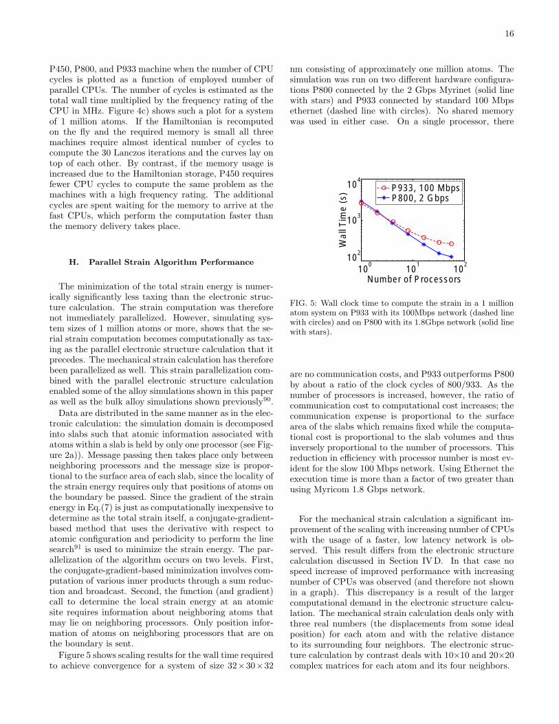
16
P450, P800, and P933 machine when the number of CPUcycles is plotted as a function of employed number ofparallel CPUs. The number of cycles is estimated as thetotal wall time multiplied by the frequency rating of theCPU in MHz. Figure 4c) shows such a plot for a systemof 1 million atoms. If the Hamiltonian is recomputedon the fly and the required memory is small all threemachines require almost identical number of cycles tocompute the 30 Lanczos iterations and the curves lay ontop of each other. By contrast, if the memory usage isincreased due to the Hamiltonian storage, P450 requiresfewer CPU cycles to compute the same problem as themachines with a high frequency rating. The additionalcycles are spent waiting for the memory to arrive at thefast CPUs, which perform the computation faster thanthe memory delivery takes place.
H. Parallel Strain Algorithm Performance
The minimization of the total strain energy is numer-ically significantly less taxing than the electronic struc-ture calculation. The strain computation was thereforenot immediately parallelized. However, simulating sys-tem sizes of 1 million atoms or more, shows that the se-rial strain computation becomes computationally as tax-ing as the parallel electronic structure calculation that itprecedes. The mechanical strain calculation has thereforebeen parallelized as well. This strain parallelization com-bined with the parallel electronic structure calculationenabled some of the alloy simulations shown in this paperas well as the bulk alloy simulations shown previously90.
Data are distributed in the same manner as in the elec-tronic calculation: the simulation domain is decomposedinto slabs such that atomic information associated withatoms within a slab is held by only one processor (see Fig-ure 2a)). Message passing then takes place only betweenneighboring processors and the message size is propor-tional to the surface area of each slab, since the locality ofthe strain energy requires only that positions of atoms onthe boundary be passed. Since the gradient of the strainenergy in Eq.(7) is just as computationally inexpensive todetermine as the total strain itself, a conjugate-gradient-based method that uses the derivative with respect toatomic configuration and periodicity to perform the linesearch91 is used to minimize the strain energy. The par-allelization of the algorithm occurs on two levels. First,the conjugate-gradient-based minimization involves com-putation of various inner products through a sum reduc-tion and broadcast. Second, the function (and gradient)call to determine the local strain energy at an atomicsite requires information about neighboring atoms thatmay lie on neighboring processors. Only position infor-mation of atoms on neighboring processors that are onthe boundary is sent.
Figure 5 shows scaling results for the wall time requiredto achieve convergence for a system of size 32×30×32
nm consisting of approximately one million atoms. Thesimulation was run on two different hardware configura-tions P800 connected by the 2 Gbps Myrinet (solid linewith stars) and P933 connected by standard 100 Mbpsethernet (dashed line with circles). No shared memorywas used in either case. On a single processor, there
100
101
102
102
103
104
Number of Processors
Wal
l Tim
e (s
)
P800, 2 GbpsP933, 100 Mbps
FIG. 5: Wall clock time to compute the strain in a 1 millionatom system on P933 with its 100Mbps network (dashed linewith circles) and on P800 with its 1.8Gbps network (solid linewith stars).
are no communication costs, and P933 outperforms P800by about a ratio of the clock cycles of 800/933. As thenumber of processors is increased, however, the ratio ofcommunication cost to computational cost increases; thecommunication expense is proportional to the surfacearea of the slabs which remains fixed while the computa-tional cost is proportional to the slab volumes and thusinversely proportional to the number of processors. Thisreduction in efficiency with processor number is most ev-ident for the slow 100 Mbps network. Using Ethernet theexecution time is more than a factor of two greater thanusing Myricom 1.8 Gbps network.
For the mechanical strain calculation a significant im-provement of the scaling with increasing number of CPUswith the usage of a faster, low latency network is ob-served. This result differs from the electronic structurecalculation discussed in Section IV D. In that case nospeed increase of improved performance with increasingnumber of CPUs was observed (and therefore not shownin a graph). This discrepancy is a result of the largercomputational demand in the electronic structure calcu-lation. The mechanical strain calculation deals only withthree real numbers (the displacements from some idealposition) for each atom and with the relative distanceto its surrounding four neighbors. The electronic struc-ture calculation by contrast deals with 10×10 and 20×20complex matrices for each atom and its four neighbors.

17
V. BULK MATERIAL PARAMETERIZATIONS
AND PROPERTIES
A. Genetic Algorithm-Based Fitting
Electronic structure calculations in the lowest conduc-tion and the highest valence band require a good param-eterization of the band gaps, effective masses and band-anisotropies (for the holes). One of the drawbacks of theempirical tight-binding models is that there is no simplerelation between these physical observables and the or-bital energies. The analytical formulas that have beendeveloped in the past42–44 serve as a guide for the gen-eral capability of a particular model and show that theoptimization space is not smooth. The fitting of the pa-rameters using these formulas has led to dramatic im-provements in the simulation capabilities of high perfor-mance resonant tunneling diodes5,6, although the processremained tedious at best.
A very nice and diligent parameterization of thesp3d5s∗ model has been published by Jancu et al.40. Alarge number of the technically relevant III-V materialsas well as elemental semiconductors have been parame-terized in their work. They have also optimized orbital-dependent distance scaling exponents η to fit strain-dependent quantities such as deformation potentials. Toenhance the performance of the model with strain in alayered superlattice configuration Jancu et al. have de-veloped a method where the d orbital on-site energy isshifted as a function of strain. For the general 3-D elec-tronic structure case that is subject to this work, a moregeneral treatment of the on-site energies as a function ofstrain must be included. In the NEMO 3-D implementa-tion of the tight-binding model, all on-site energies canbe shifted due to strain in an arbitrary 3-D configuration.
To automate the fitting of the orbital tight-binding pa-rameters to the desired bulk material properties40,92,93
a genetic algorithm (GA) based software package. Thedetails of this algorithm and several improved materialparameterizations are described elsewhere45,46 was devel-oped. The general idea of the GA is the stochastic explo-ration of a parameter space with a large set of individuals,which represent different parameter configurations. Theindividuals are measured against a certain desired fitnessfunction and ranked. Some of the individuals (for exam-ple 10% of the worst performers) are thrown out of thegene pool and replaced by new individuals that are de-rived from better performers by cross-over and mutationoperations. The parameterizations used in this work havebeen obtained using this GA approach, starting from ear-lier parameterizations40,42–44.
The following sections present the parameterizationdata, and the resulting unstrained and strained bulk-properties.
TABLE II: sp3s∗ tight-binding parameters for GaAs and InAs.All energies are in units of eV and the lattice constant isin units of nm. For this parameterization all relevant off-diagonal stain scaling parameters are set to η = 2 and alldiagonal strain scaling parameters are set to C =0.
Parameter GaAs InAs
lattice/(nm) 0.56660 0.60583
E(sa) -8.51070 -9.60889
E(pa) 0.954046 0.739114
E(sc) -2.77475 -2.55269
E(pc) 3.43405 3.71931
E(s∗a) 8.45405 7.40911
E(s∗c) 6.58405 6.73931
V (s, s) -6.45130 -5.40520
V (x, x) 1.95460 1.83980
V (x, y) 4.77000 4.46930
V (sa, pc) 4.68000 3.03540
V (sc, pa) 7.70000 6.33890
V (s∗a, pc) 4.85000 3.37440
V (pa, s∗c) 7.01000 3.90970
∆a 0.42000 0.42000
∆c 0.17400 0.39300
Eoffsetv 0.00000 0.22795
B. Parameter Tables and Bulk Properties
Table II lists the parameters that enter the sp3s∗ modelused in this paper. The parameterization for InAs wasobtained from a GA, while the GaAs data was originallydelivered by Boykin to the NEMO 1-D project. No ef-fort has been made in this parameterization to fit theoff-diagonal or the diagonal matrix element strain cor-rections. All off-diagonal matrix elements are scaled withthe ideal exponent71 of η=2 and the diagonal correctionis set to zero.
An explicit InAs valence band offset vs. GaAsof 0.22795 is used in this parameterization. Thesp3d5s∗ parameterization in contrast is based on commonatom potentials and has the valence band offset built intothe parameter set.
Table III shows the complete parameterization of GaAsand InAs in our sp3d5s∗ tight-binding model includingthe off-diagonal and diagonal strain scaling parameters.In this model a good fit based on common atomic po-tentials of the As in the GaAs and InAs has been ob-tained. A valence band offset of the unstrained mate-rials of 0.2259eV is built into the parameter set. Thesp3d5s∗ model is rich enough in its physical content toenable the fitting of GaAs, InAs, and AlAs with comonAs potentials and built-in valence band offsets. Commonatom potentials and built-in valence band offsets cannotbe achieved in the sp3s∗ model, unless some of the fittingrequirements are severely relaxed.
Table IV summarizes the major unstrained bulk mate-

18
rial properties that have been targeted in the sp3s∗ andsp3d5s∗ parameterization for GaAs and InAs. The tar-get parameters are taken from various experimental andtheoretical references40,92,93. The major parameters ofinterest are associated with the lowest conduction andthe two highest valence bands. In Table IV these prop-erties are separated by a horizontal line from parametersthat are outside these central bands of interest. The up-per and lower band edges as well as the minimum pointin the [111] direction kL are included in the optimizationtarget with a relatively small weight. These propertiesare included in the optimization to preserve an ”overall”good shape of the bands outside the major interest. Ifthey are not included, upper and lower bands will dis-tort significantly to aid the desired perfect properties ofthe central bands. This distortion can lead to undesiredband crossings on and off the zone center.
Also included (yet not shown in the table) is anotherrestriction on the GaAs and InAs parameters to alloy“well” within the virtual crystal approximation (VCA).It has been found that parameter sets that representthe individual GaAs and InAs quite well can result ina InxGa1−xAs alloy representation that has completelywrong behavior of the bands as a function of x (dramaticnon-linear bowing). Typically a target that linearly in-terpolates the central conduction and valence band edgesfor InxGa1−xAs from GaAs and InAs as a function of xis included. Bowing is not built into these VCA param-eters, but establishes itself in the 3-D disordered system(see reference [90] for an AlxGa1−xAs example and Sec-tion VI B for a discussion on InxGa1−xAs).
Compared to the sp3s∗ model, the sp3d5s∗ model gen-erally provides better fits to the hole effective masses andthe electron effective masses at Γ and L. The failure of thesp3s∗ model to properly reproduce the transverse effec-tive mass on the ∆ line towards X is well understood45.The sp3d5s∗ model does allow the proper modeling of theeffective masses in that part of the Brillouin zone.
Figure 6 shows the bulk dispersion of GaAs (left col-umn) and InAs (right column) computed from the tight-binding parameters listed in Tables II and III withoutstrain. The dispersion corresponding to the sp3s∗ modelis plotted in a dashed line and compared to the resultsfrom the sp3d5s∗ model in a solid line. The first rowin Figure 6 shows the bands in a relatively large energyrange including the lowest valence band in the modelsas well as several excited conduction bands. The secondrow in Figure 6 zooms in on the central bands of interest.The sp3s∗ and sp3d5s∗ model agree reasonably well witheach other at the Gamma point in their energies as wellas their curvatures of the central bands of interest. Offthe zone center the deviation between the two modelsbecome significant. Some of the band energies are hardto probe experimentally and are only known from othertheoretical models40,92,93. However the conduction bandenergies at X and L and their corresponding masses arewell known, and the sp3s∗ model does fail to deliver a
-10
-5
0
5
Ene
rgy
(eV
)
-10
-5
0
5
-2
0
2
Ene
rgy
(eV
)
spdssps
-2
0
2
4
L Γ XMomentum
L Γ XMomentum
GaAs
GaAsInAs
InAs
(a) (b)
(c) (d)
FIG. 6: E(k) dispersion for GaAs (left column) and InAs(right column) computed with the sp3s∗ (dashed line) andsp3d5s∗ (solid line model).
good fit. The sp3s∗ model generally appears to deviatestrongly from the sp3d5s∗ model in the [111] directioneven for the central bands of interest.
C. Band Edges as a Function of Strain
The deformation of atomic positions from their idealvalues in a relaxed semiconductor crystal modifies theinteraction between atomic neighbors and therefore theelectronic bandstructure. The ability to form strainedstructures without defects opens a new design space ex-ploited by many commercially relevant devices, includ-ing, for example, InGaAsP-based laser diodes operatingat 1.55µm. Although good qualitative results have beenobtained for the strain-dependence of the effects of inter-est in these devices94, very precise measurements of allthe empirical parameters that influence strain are stilllacking. The baseline strain parameterization to whichthe calculation is compared and fitted to has been pre-sented by Van de Walle95. Van de Walle’s parameteri-zation is not purely empirically based, but partially de-pendent on a k ·p expansion following Pollak and Car-dona96. For this work, Van de Walle’s parameters havebeen slightly modified to represent room temperaturebandgaps.
Figure 7 shows the conduction and valence band edgesfor GaAs (left column) and InAs (right column) as a func-tion of hydrostatic strain (top row) and bi-axial strain(bottom row). Three parameterizations are compared ineach graph: 1) reference data by Van de Walle (dashedline), 2) data computed from the sp3d5s∗ model (cir-cles), and 3) data computed from the sp3s∗ model (solidline). The test application in this paper is the mod-eling of a strained InGaAs system grown on top of a

19
GaAs substrate. Since InAs has a larger lattice constantthan GaAs one needs to model effects on InAs as it iscompressed towards the GaAs lattice constant (7% neg-ative strain). GaAs bonds, by contrast, are expectedto be stretched towards the InAs bondlength at inter-faces (positive strain). Since the InGaAs quantum dotsgrown on GaAs which are considered in the next twosectins VI and VII are significantly larger in their widththan their height, one can expect the strain in the dotto be mostly bi-axial. However some hydrostatic straindistributions can be expected as well, due to the finiteextent of the InAs quantum dots inside the GaAs buffer.The z-directional strain component in the bi-axial straincase is computed as εzz =2 c12
c11
εxx and εyy =εxx.Both tight-binding models follow the trends set by
the Van de Walle reference reasonably well. Generallyspeaking the sp3d5s∗ model performs better than thesp3s∗ model (which actually was not optimized for itsstrain performance). It has been particularly hard toimprove the under-prediction of the InAs band gap (Fig-ure 7d)) for large compressive bi-axial strain. The rea-sonably good fit has been obtained by compromising thefit of the conduction band under hydrostatic compressivestrain. In contrast, the InAs valence bands has not notposed any problem at all to be fit to the Van de Walledata.
-0.02 0 0.02 0.04
0.0
1.0
2.0
Hydrostatic Strain εxx
=εyy
=εzz
GaA
s E
nerg
y (e
V)
-0.06 -0.04 -0.02 0-0.5
0.0
0.5
1.0
1.5
2.0
Hydrostatic Strain εxx
=εyy
=εzz
InA
s E
nerg
y (e
V)
spdsspsWalle
-0.02 0 0.02 0.04 0.06-0.5
0.0
0.5
1.0
1.5
Biaxial Strain εxx
=εyy
GaA
s E
nerg
y (e
V)
-0.06 -0.04 -0.02 0 0.02
-0.5
0.0
0.5
1.0
Biaxial Strain εxx
=εyy
InA
s E
nerg
y (e
V)
(a) (b)
(c)
(d)
GaAs
GaAs
InAs
InAs
EcEc
E =E HH LHE =E HH LH
Eso
Eso
Eso
Ec
Ec
E HH
E LH
E HH
E LH
Eso
FIG. 7: GaAs and InAs conduction band, heavy-hole, light-hole and split-off band edges as a function of hydrostatic andbi-axial strain. Dashed line from parameterization of Vande Walle95. Circles from sp3d5s∗ model and solid line fromsp3s∗ model.
D. Effective Masses as a Function of Strain
Previous nanoelectronic transport simulations haveshown that it is essential5–7 to properly model the band
edges and effective masses in the heterostructure. In asingle band model the dependence of eigen-energy of aconfined state is inversely proportional to the effectivemass. With the strong dependence of the band-edgeson the strain shown in Figure 7 one can also expect astrong dependence of the effective masses on the strain.Figure 8 shows the electron (first row), light hole (sec-ond row), and heavy hole (third row) effective masses forGaAs (first column) and InAs (second column) as a func-tion of hydrostatic strain (lines with circles) and bi-axialstrain (lines without symbols) for the sp3s∗ (dashed line)and the sp3d5s∗ model (solid line) computed in the [001]direction. Negative strain values correspond to compres-sive strain. For the electron mass the sp3s∗ and the
0
0.05
0.10spsspds
0
0.05
0.1
m*(
el) hydro
bi-ax
-0.02 0 0.02 0.04 0.060.35
0.40
0.45
0.50
Strain
m*(
HH
)
-0.06 -0.04 -0.02 0 0.02
0.35
0.40
0.45
Strain
0
0.10
0.20
0.30
0
0.10
0.20m
*(LH
)
no sym
(a) (b)
(f)
(d)(c)
(e)GaAs
GaAs InAs
InAs
GaAs InAs
FIG. 8: Electron, heavy hole (HH) and light-hole (LH) effec-tive masses in the [001] direction as a function of hydrostatic(circles) and bi-axial (no symbols) strain for the sp3s∗ andthe sp3d5s∗ model. Left column GaAs, right column InAs.Negative strain numbers correspond to compressive strain.
sp3d5s∗ model show roughly the same trends for GaAs aswell as InAs. The GaAs mass drops towards the smallerInAs mass as GaAs is stretched towards InAs. In InAsthe electron mass is increased towards the heavier GaAsmass as the material is compressed towards GaAs. Thesp3d5s∗ model shows a larger difference between the effectof hydrostatic and bi-axial strain than the sp3s∗ model.
The change in the effective mass in InAs under com-pressive bi-axial strain is quite important. Under 7%bi-axial strain the effective mass approximately doubles.This increase in the effective mass lowers the confinementenergies in the the quantum dots, effectively increasingthe confinement. The spacing between the confined elec-
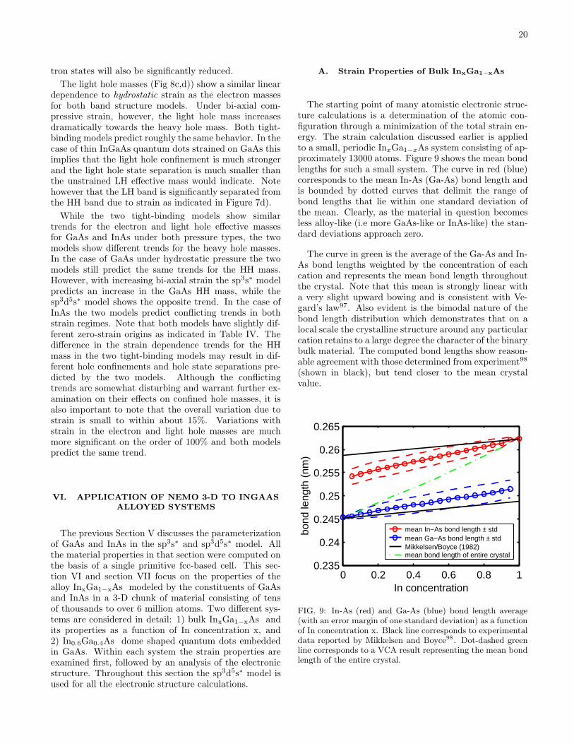
20
tron states will also be significantly reduced.
The light hole masses (Fig 8c,d)) show a similar lineardependence to hydrostatic strain as the electron massesfor both band structure models. Under bi-axial com-pressive strain, however, the light hole mass increasesdramatically towards the heavy hole mass. Both tight-binding models predict roughly the same behavior. In thecase of thin InGaAs quantum dots strained on GaAs thisimplies that the light hole confinement is much strongerand the light hole state separation is much smaller thanthe unstrained LH effective mass would indicate. Notehowever that the LH band is significantly separated fromthe HH band due to strain as indicated in Figure 7d).
While the two tight-binding models show similartrends for the electron and light hole effective massesfor GaAs and InAs under both pressure types, the twomodels show different trends for the heavy hole masses.In the case of GaAs under hydrostatic pressure the twomodels still predict the same trends for the HH mass.However, with increasing bi-axial strain the sp3s∗ modelpredicts an increase in the GaAs HH mass, while thesp3d5s∗ model shows the opposite trend. In the case ofInAs the two models predict conflicting trends in bothstrain regimes. Note that both models have slightly dif-ferent zero-strain origins as indicated in Table IV. Thedifference in the strain dependence trends for the HHmass in the two tight-binding models may result in dif-ferent hole confinements and hole state separations pre-dicted by the two models. Although the conflictingtrends are somewhat disturbing and warrant further ex-amination on their effects on confined hole masses, it isalso important to note that the overall variation due tostrain is small to within about 15%. Variations withstrain in the electron and light hole masses are muchmore significant on the order of 100% and both modelspredict the same trend.
VI. APPLICATION OF NEMO 3-D TO INGAAS
ALLOYED SYSTEMS
The previous Section V discusses the parameterizationof GaAs and InAs in the sp3s∗ and sp3d5s∗ model. Allthe material properties in that section were computed onthe basis of a single primitive fcc-based cell. This sec-tion VI and section VII focus on the properties of thealloy InxGa1−xAs modeled by the constituents of GaAsand InAs in a 3-D chunk of material consisting of tensof thousands to over 6 million atoms. Two different sys-tems are considered in detail: 1) bulk InxGa1−xAs andits properties as a function of In concentration x, and2) In0.6Ga0.4As dome shaped quantum dots embeddedin GaAs. Within each system the strain properties areexamined first, followed by an analysis of the electronicstructure. Throughout this section the sp3d5s∗ model isused for all the electronic structure calculations.
A. Strain Properties of Bulk InxGa1−xAs
The starting point of many atomistic electronic struc-ture calculations is a determination of the atomic con-figuration through a minimization of the total strain en-ergy. The strain calculation discussed earlier is appliedto a small, periodic InxGa1−xAs system consisting of ap-proximately 13000 atoms. Figure 9 shows the mean bondlengths for such a small system. The curve in red (blue)corresponds to the mean In-As (Ga-As) bond length andis bounded by dotted curves that delimit the range ofbond lengths that lie within one standard deviation ofthe mean. Clearly, as the material in question becomesless alloy-like (i.e more GaAs-like or InAs-like) the stan-dard deviations approach zero.
The curve in green is the average of the Ga-As and In-As bond lengths weighted by the concentration of eachcation and represents the mean bond length throughoutthe crystal. Note that this mean is strongly linear witha very slight upward bowing and is consistent with Ve-gard’s law97. Also evident is the bimodal nature of thebond length distribution which demonstrates that on alocal scale the crystalline structure around any particularcation retains to a large degree the character of the binarybulk material. The computed bond lengths show reason-able agreement with those determined from experiment98
(shown in black), but tend closer to the mean crystalvalue.
0 0.2 0.4 0.6 0.8 10.235
0.24
0.245
0.25
0.255
0.26
0.265
In concentration
bond
leng
th (
nm)
mean In−As bond length ± std mean Ga−As bond length ± std Mikkelsen/Boyce (1982)mean bond length of entire crystal
FIG. 9: In-As (red) and Ga-As (blue) bond length average(with an error margin of one standard deviation) as a functionof In concentration x. Black line corresponds to experimentaldata reported by Mikkelsen and Boyce98. Dot-dashed greenline corresponds to a VCA result representing the mean bondlength of the entire crystal.

21
B. Electronic Properties of Bulk InxGa1−xAs
With the atomic configurations the electronic proper-ties of the In0.6Ga0.4As system can be obtained. Fig-ure 10 compares the experimentally measured93 energygap (shown in green) of InxGa1−xAs as a function of Inconcentration x with numerical results, obtained in twodifferent ways. The red curve is the VCA result, obtainedby diagonalizing the tight-binding Hamiltonian on a sin-gle unit cell with periodic boundary conditions, in whichthe cation-anion coupling potentials are determined bya strict average of the In-As and Ga-As coupling poten-tials. The lattice constant of the single cubic unit cell isdetermined by Vegard’s law97. The resulting energy gapis mostly linear, but displays a very slight upward bow-ing. The blue curve is obtained by diagonalizing the fullHamiltonian of the alloyed system. The system size issufficiently large that variations of the energy gap due toconfigurational noise (see analysis in Section VII) is notvisible on the energy scale shown in the figure. The deter-mined energy gap differs from the VCA result by a max-imum of 60 meV and displays a slight downward bowing,although significantly less than that of the experimen-tal result93. The linear behavior in the VCA computedbandgap is included in the tight-binding parameter fit-ting as discussed in Section V B. The random cation dis-order in the 3-D bulk system can, therefore, be attributedwith the bowing. In similar AlxGa1−xAs simulations90
much better agreement between the 3-D simulation andthe experimental results has been achieved. Some bowingmight have to be built into the VCA based parameteriza-tion of GaAs and InAs to accommodate the larger bowingin the InxGa1−xAs system compare to the AlxGa1−xAs.
0 0.2 0.4 0.6 0.8 1
0.4
0.6
0.8
1
1.2
1.4
In concentration (x)
Ene
rgy
gap
(eV
)
experimentalloyvca
FIG. 10: Experimentally measured93 energy gap (solid line)of InxGa1−xAs as a function of In concentration x comparedwith results based on the 3-D random alloy simulation (cir-cles) and a virtual crystal approximation (stars).
C. Strain in an Alloyed Quantum Dot
This section demonstrates an example of the straincalculation in an alloyed quantum dot using NEMO 3-D. The model problem is a dome-shaped In0.6Ga0.4AsQD of diameter 30 nm and height 5 nm enclosed in aGaAs box of size 74× 74× 28nm3. The entire structure,which contains roughly 6.3 million atoms, is allowed toexpand freely to minimize the total strain energy (nofixed boundary conditions). The diagonal part of the lo-cal strain tensor is examined along the x-axis, which lieshalfway between the top and bottom of the dome andparallel to its base. Figures 11a) and 11b) show thecomponents εxx (blue), εyy (green), εzz (red), and Tr(ε)(black) of the local strain tensor of the primitive cell cen-tered about the Ga and In cations respectively. Withinthe QD, the In-As bonds (see Figure 11b) are compres-sively strained roughly equally in the x and y directions(approximately 4.69% and 4.99% respectively). Thereis a very slight tensile strain in the z direction (∼ 0.02%). There are three competing effects that determine thesign and magnitude of this strain. First, there is a neg-ative hydrostatic component due to the smaller latticeconstant of the buffer. Second, the flatness of the domemeans that close to the center of the QD, the strain fieldshould approach that of quantum well in which the cu-bic cell is compressively strained laterally (i.e. in x andy) and stretched in z. Finally, the presence of nearbyGa cations provides an additional negative hydrostaticcomponent to the strain. The combination of these threeeffects gives rise to a large biaxial compressive strain anda nearly vanishing strain component normal to the flatdome.
The Ga cations within the dome (see Figure 11a) aresubject to only one of these effects, that of the biax-ial strain of nearby In-As bonds. Interestingly, the Ga-As bond lengths are reduced laterally (-1.98% (x) and-1.90% (y)) from their bulk values. This reduction islikely an effort to match the very large z-component ofthe In-As bondlengths. The resulting average tension inthe z direction is 2.14%.
Just outside the dome, along x, the Ga atoms suffertensile strain in y and in z (although more so in z) tomatch the effective lattice constant on the boundary ofthe dome. This stretching results in compressive strainalong x as indicated in Figure 11(a) by the negative valueof εxx outside the QD.
D. Local Band Structure in an Alloyed Quantum
Dot
Figure 12 shows the effect of the deformation of theprimitive cells under strain on the local electron and holeband structure. Each point represents a “local” eigen-energy obtained by constructing a bulk solid from theprimitive cell formed from the four As anions enclosing

22
-20 0 20-0.06
-0.04
-0.02
0
0.02
0.04
0.06
Position along x (nm)
Str
ain
ε xx
ε yy
ε zz
Tr{ε}
(a) Ga-As bonds
-10 -5 0 5 10-0.15
-0.10
-0.05
0
0.05
Position along x (nm)
Str
ain
εxx εyy εzz Tr{ }ε(b) In-As bonds
FIG. 11: Components of strain tensor for primitive cells cen-tered around (a) Ga and (b) In cations along an axis midwayfrom the top and bottom of the dome and parallel to its base.
each cation. One sees that outside the QD, the tensilestrain the GaAs cells experience reduces the conductionband edge slightly from its bulk value and splits the de-generate valence band (shown in black) into heavy hole(HH) and light hole (LH) bands.
Within the QD, both GaAs and InAs cells are squeezedlaterally resulting in a increase in local electron eigen-energies. The resulting mean electron band edge alongthe x-axis and within the QD is indicated by the thinsolid line. Biaxial compressive strain also raises (low-ers) the local HH (LH) eigen-energies within the QD forboth InAs and GaAs cells, and, again, the average HHQD band edge is indicated by a thin solid line. Clearly,the random distribution induces a large variation in localpotentials, which will shortly be seen to strongly affectshallow hole states.
-20 0 201.0
1.1
1.2
1.3
1.4
1.5
1.6
Ene
rgy
(eV
)
Position along x (nm)
InAs (EL)GaAs (EL)
(a)
-20 0 20-0.2
-0.1
0
0.1
0.2
0.3
0.4
Ene
rgy
(eV
)
Position along x (nm)
InAs (HH)InAs (LH)GaAs (HH)GaAs (LH)
(b)
FIG. 12: “Local” conduction (a) and valence (b) band edgesdetermined by imposing periodic boundary conditions on aprimitive cell constructed from the four anions surrounding agiven cation.
E. Wave Functions in an Alloyed Quantum Dot
This section examines the effect of disorder on electronand hole eigenfunctions. Three different alloy configura-tions are examined for the same quantum dot size, shape,and number of included atoms – two different random al-loy configurations that differ only by the random place-ment of the In and Ga atoms in the In0.6Ga0.4As, anda VCA-based configuration without spatial disorder. Inthe VCA representation all cations within the QD are ofa fictitious type “In0.6Ga0.4” in which all tight-bindingparameters (and the strain parameters) are linearly aver-aged between InAs and GaAs parameters106. This casecorresponds most closely to a jellium description and isused as our baseline reference. The disordered wave func-tions are shown to be significantly different from each

23
other as well as from the homogeneous VCA system wave-functions. A detailed statistical analysis of the computedeigen energies as a result of the wave function variationsis deferred to Section VII. The quantum dot and com-position is identical to the discussion above. However,to reduce the computational expense, the GaAs buffer isreduced to a size of 74×74×15 nm3 and contains roughly3.6 million atoms.
Figure 13 shows four different representations of theground state electron wave function obtained for threedifferent configurations. The first column shows resultsfor a VCA implementation. The other two columns dis-play results for two separate random distributions of Inand Ga atoms within the QD. The first row depicts scat-ter plots of the probability density, where the red pointsmark atomic sites where the probability density exceedsone-third of the maximum value, and green and bluepoints mark higher values. Clearly there is not much dif-ference between the three plots except that the VCA re-sult is somewhat smoother. Also, the VCA plot is slightlylarger indicating a slower decay as one moves away fromthe central axis of the QD. The next two rows are con-tour plots of a slice parallel to the base of the dome andmid-way up in height. Here, the impact of the disorderon the wave function is quite evident, although the s-likecharacter of the wave function still closely resembles thatof the homogeneous QD. Also, the difference between thetwo disordered QDs is not significant. The eigenenergiesdiffer by about 1.38meV. The last row depicts a surfaceplot of the wave function (normalized to unity over theentire simulation domain) and shows that the homoge-nous result is a smoothed version of the disordered wavefunction with a lower maximum.
Figure 14 shows a set of hole wave functions analogousto the those shown in Figure 13 for the electron groundstate. First note that the VCA scatter plot looks similarto the ground state VCA electron wavefunction, exceptthat it is flatter. The stronger localization in the z di-rection reflects the greater confinement due to the largerhole mass relative to that of the electron. The larger holemass also makes the wave function more susceptible toperturbations in the local potential. This effect is demon-strated in the three hole scatter plots, where the disorderstrongly changes the appearance of the wave function.Note, also, that different placements of cations can pro-duce noticeably different results as seen in the contourplots where the location of the wave function peaks varyby several nm. The greater localization in systems withdisorder also manifests itself by the much larger peaks inthe surface plots, where the probability density is, again,normalized to unity over the entire simulation domainin each of the three cases. The hole eigenvalues differby -3.44meV compared to a difference of +1.38meV forthe electrons. A more detailed statistical analysis of thedistribution of eigenvalues is the topic of the followingsection VII.
Figure 15 shows the six lowest electron (rows 1 and 2)
and hole (rows 3 and 4) states for a similar system withthe same dome dimensions, but enclosed in a buffer ofsize 56×56×24 nm3. First, note that the electron statesmore closely resemble the states one would expect from ahomogeneous QD. Also, the three lowest hole states cor-respond well to their electron counterparts, but higherenergy states differ. There are two possible explana-tions. First, the Lanczos algorithm might not have yetconverged on an intermediate eigenvalue. Second, thedisorder in the system may rearrange the ordering of theeigenstates. Note that there exist several pairs of states(electron 2 and 3; electron 5 and 6; and hole 2 and 3) thatstem from degenerate states in the homogeneous system,yet the disorder splits their eigenenergies by up to 1.4meV. Since this splitting due to disorder is roughly thesame order of magnitude as the separation of the excitedstates, it is conceivable that the disorder can rearrangethe ordering of the eigenstates.
VII. STATISTICAL ANALYSIS OF RANDOM
DISORDER IN ALLOYED QUANTUM DOTS
A. Set-up of the Numerical Experiment
This section considers the same dome shapedIn0.6Ga0.4As quantum dot as the previous sections.Since the In and Ga ions inside the alloyed dot are ran-domly distributed, different alloy configurations exist andoptical transition energies from one dot to the next mayvary, even if the size and the shape of the dot are as-sumed to be fixed. This section seeks to answer thequestion: What is the minimal optical line width thatcan be expected for such an alloyed dot neglecting anyexperimental size variations? To enable the simulationof about 1000 different configurations the required simu-lation time was reduced by three additional approxima-tions / simplifications: 1) the surrounding GaAs bufferis reduced to 5nm in each direction around the quantumdot. This results in a total simulation domain of approxi-mately 1,000,000 atoms with about 718,000 atoms in thequantum dot itself, 2) the use of sp3s∗ model instead ofthe sp3d5s∗ model (a reduction of the required computetime by about 4×), and 3) the computation of the eigen-values without the corresponding eigenvectors (resultingin a reduction of compute time by exactly a factor of two).With these approximations and simplifications the wallclock time to obtain one set of eigenvalues for one par-ticular alloy configuration took about 25 minutes on 31processors of P933. 1000 different alloy samples thereforerequired approximately 420 hours or 17.4 days wall clocktime or about 13,000 hours or 538 days single processorcomputing time. The mechanical strain is minimized us-ing a valence force field method34,35 as discussed in Sec-tion III D for each alloy configuration. Changing the ran-dom seed of the random number generator generates therandom alloy configurations. The reduced GaAs buffer

24
size tends to increase the optical band-to-band transitionenergy by simultaneously raising the electron energy andlowering the hole energy. The use of the sp3s∗ mode com-promises some of the accuracy of the electronic structuredue to strain (see discussions in Section V). In particularone can expect that the optical band gap will be under-predicted since the bi-axially strained InAs band gap isunder predicted in bulk (see Figure 7d). While the ab-solute energies are shifted from the experimental data,one can, however, still expect that the distribution andextent of the variations in the eigenvalues generated bythe alloy disorder around the mean energies are indepen-dent of the mean, and therefore independent of the buffersize99
NEMO 3-D currently supports two disorder models.The first makes the simplifying assumption that neigh-boring cations are completely uncorrelated so that thespecies at a particular cation site is determined randomlyaccording to the expected concentration x and indepen-dently of the configuration of the remainder of the su-percell. This disorder is referred to as atomic granularity(AG) in this paper. The second model of compositionaldisorder, increases the granularity of the disorder fromthe atomic level to that of the cubic cell, so that all fourcations within a unit cell are of the same species resultingin cell granularity (CG). Within the AG model the cationconcentrations can be allowed to vary statistically or theycan be pinned to a single value, enabling the simulationof pure configuration noise.
Previous work90 on an unstrained AlxGa1−xAs bulksystem showed that concentrational noise (concentrationx varies statistically) dominates over the configurationalnoise (fixed concentration x) by at least one order ofmagnitude in the standard deviations in the conductionand valence band edge. The pure configurational noiseis therefore not considered here anymore, since there isexperimentally no exact control over the concentration xanyhow. Instead the two granularity models are exam-ined in more detail.
B. Statistical Analysis of State Distributions
560 and 490 samples were evaluated for the atomicgranularity (AG) and cell granularity (CG), respectively.Figure 16 provides a graphical analysis of some of thedata obtained. The first row of Figure 16 shows his-tograms of the valence band, conduction band, and band-gap energies for the 560 atomic granularity samples using30 samples per bin. The standard deviation of the va-lence band states (σAG
v = 0.9meV ) is smaller than thatof the conduction band states (σAG
c =1.4meV ). This dif-ference arises from the heavier hole mass and the higherdensity of states as observed in bulk alloy simulations90.The second row of Figure 16 compares the histogramsof the first row (atomic granularity) to the correspond-ing histograms obtained in the model of cell granularity.
Similar to the pure bulk alloy results90 the cell granu-larity results in standard deviations of the energies thatare larger than the atomic granularity deviations(σAG
c =2.8meV ,σAG
v =1.9meV ). For this particular dot size thedifference between AG and CG is about a factor of two.Similar to the bulk simulations90 a change in the valenceband state state energy average that is larger than theshift in the conduction band energy average can be ob-served (∆Ev = ECG
v −EAGv = 0.1938eV − 0.1862eV =
7.7meV ,∆Ec = ECGc −EAG
c = 1.2291eV − 1.2298eV =−0.8meV ). Again an overall reduction in the opti-cal band gap is the result of the increased granularity(∆EG =ECG
G −EAGG =1.0352eV −1.0436eV =−8.4meV ).
The band-gap deviation is roughly additive from thevalence and conduction band deviations. This additivebehavior indicates a correlation between the conductionand valence state energies. This correlation can be ex-plored with a scatter plot of Ec versus Ec for all sam-ples as shown in Figure 16g). A linear regression of thetwo scatter plots result in Ec = 1.4685 − 1.2823Ev andEc =1.405− 1.1939Ev, for the AG and CG distributions,respectively, with a good regression quality of R≈0.8. Arelation between these strongly correlated energy valuesand the bulk band structure is discussed in the followingSection VII C.
The data can also be analyzed with respect to itsdependence of the actual In concentration x in theInxGa1−xAs alloy. Figure 16i) shows a histogram of theIn distribution in the CG model. The expectation valueis the desired 0.6, the standard deviation of 0.0016. Thisdeviation is purely determined by the statistical variationas a function of systems size90 (about 718,000 atoms inthe dot in this case) and the random selection with expec-tation of 0.6. The statistical variation is certainly smallerthan the experimental control on the alloy concentrationand one can expect the experimental uncertainty in thealloy concentration to be significantly larger.
Figure 16h) shows a scatter plot of the conductionband state energies computed in the CG model as afunction of their corresponding In concentration. Thescatter plot appears more like a round blob, indicat-ing a weak correlation, and indeed the linear regres-sion to Ec = 1.4871 − 0.43015x is characterized by asmall regression quality R = 0.24. A similarly weakcorrelation can be found for the valence band states:Ev = 0.04574 + 0.24682x with R = 0.21. This weak cor-relation of Ec and Ev with x is in contrast to a strongcorrelation we have seen in our bulk simulations90.
C. Quantized Energy Comparison Against Bulk
Data
The quantized single particle energies in the quantumdot are determined by a multitude of influences. The firstorder effects are based on the underlying semiconductorband structure, the confinement by the heterostructure

25
interfaces, the composition of the material and the sizeof the dots. Effects due to disorder and electron-electroninteractions have to be considered second order effects.The discussion in this section examines the correlationbetween the quantized Ec and Ev energies shown in Fig-ure 16g) and verifies that the quantized eigen-energiesshown in Figure 16 fit within the underlying semiconduc-tor band structure. This comparison serves as an overallsanity check and as a characterization of the relative im-portance of hydrostatic and bi-axial strain contributionsto the quantized states in the quantum dot.
Figure 17a) shows the bulk conduction and valenceband edge of InxGa1−xAs as a function of In concen-tration x in a VCA approximation of a single unit cell.The graphs are computed using the same GaAs and InAssp3s∗ parameter set that was used for the statistical quan-tum dot analysis in the section above. Three differ-ent strain conditions are evaluated: 1) unstrained bulk(dashed line), 2) hydrostatically compressed (εxx =εyy =εzz) to the GaAs lattice constant (dotted line), and 3) bi-axially compressed (εxx = εyy 6= εzz) to a GaAs substratein the x-y plane (solid line). It is interesting to see thatthe hydrostatically compressed InGaAs has a very smalldependence on the In concentration. The same graphalso shows the scatter plot of the quantized conductionand valence band energies as a function of actual alloycomposition.
The single cross symbols indicate the average bottomof the conduction and the average top of the valence bandin a small region of the center of the quantum dot (see thediscussion of the spatially varying local band structurein section VI D). The electron and valence band statesshow confinement energies of roughly 96meV and 50meV,respectively. The difference in the confinement energiesie of course expected due to the difference in the heavy-hole and electron masses. The placement in energy ofthe local conduction and valence band edge as well as thequantized state energies in the quantum dot indicate thatthe states inside the quantum dot are influenced by bi-axial as well as hydrostatic strain components combined.
Similar to to Figure 16h) the linear regression is shownas a red line running roughly parallel to the bulk bi-axialstrain line. Little trust can be given to the linear regres-sion lines due to their small quality values of R ≈ 0.21.However, the slopes do not conflict with the hypothe-sis that the electronic state is dominated by the bi-axialstrain shifts with some hydro-static strain shift contribu-tions.
Figure 17b) plots the data of (a) on a Ec vs. Ev coor-dinate system. Within this reference frame Figure 16g)already show a strong correlation between the quantizedEv and Ec energies with a trustworthy linear regressionof slope -1.1939. The unstrained, hydrostatically strainedand bi-axially strained bulk slopes are: -10.747, -3.5726,and -1.3186, respectively. Again one can infer a stronginfluence on the confined states by the bi-axial strain.The individual square symbols indicate the alloy compo-
sition of 60% In and the cross indicates the average localband structure value in the middle of the dot.
D. Comparison Against Experimental Data
The numerical experiment shows a mean optical tran-sition energy of about 1.04eV and a standard deviation,or associated linewidth of approximately 2 to 5meV as-suming a fixed quantum dot size and a narrow In con-centration distribution99. This corresponds to an exper-imentally reported100 linewidth of 34.6meV at an opticaltransition energy of about 1.09eV. The optical bandgapis underpredicted by about 50meV in the sp3s∗ modelused in the alloy disorder study of Section VII. Thesp3d5s∗ model used in Section VI predicts an opticalband gap of about 1.151eV, about 60meV too large com-pared to the experiment. Excitonic interactions will re-duce the optical bandgap by about 10 to 30meV. Withan experimentally observed optical line width of 34.6meVthe sp3d5s∗ model is well within the experimental andtheoretical errors. The experimental data do of courseinclude quantum dot size variations, and the actual alloyconcentration and alloy distribution are unknown. Weplan to simulate larger sample space that does includequantum dot size variations and different alloy profiles69
in the future. The major result of this simulation is theobservation that there will be a significant99 optical linewidth variation due to alloy disorder alone, even if allthe quantum dots were perfectly identical in size with awell-known alloy concentration.
VIII. CONCLUSION AND FUTURE OUTLOOK
A. Summary
This paper presents the major theoretical, numerical,and software elements that have entered into the NEMO3-D development over the past three years. The atom-istic valence-force field method is used for the determina-tion of atom positions in conjunction with the atomisticsp3s∗ and sp3d5s∗ tight-binding models to compute elec-tronic structure in systems containing up to 16 millionatoms. An eigenvalue solver that scales linearly with thenumber of atoms in the system has been demonstrated.Beowulf cluster computers are shown to be efficient com-puting engines for such electronic structure calculations.The electronic structure calculations require a signifi-cant RAM access by the CPU, and the Intel Pentium IIIbenchmarks presented in this work show that dual CPUmotherboards suffer from severe memory access prob-lems. Faster computation completion can be obtained byleaving one of the CPUs on each board idle. This sug-gests that high memory use applications do not benefit atall from a dual Pentium III motherboard. Genetic algo-rithms are used to determine the empirical parameteriza-

26
tion of the atomistic tight-binding models. The details ofthe new tight-binding model parameterizations for GaAsand InAs are discussed with respect to their unstrainedand strained bulk properties. NEMO 3-D is used to studythe effects of disorder in InxGa1−xAs bulk material andin In0.6Ga0.4As quantum dots. The bulk properties areshown to be represented well within NEMO 3-D . Thequantum dot simulations show significant distortions inthe confined electron and hole wavefunctions introducedby random cation disorder. The distortion is more pro-nounced for the hole states than the electron states andit is not visible within a smooth virtual crystal approx-imation, which resembles non-atomistic methods. Overa thousand different alloy distributed quantum dots aresimulated and a variation of the optical transition energyof several meV is observed.
B. Future Simulations
The strong variations in the electron and hole wave-functions introduced by the alloy disorder beg for theevaluation of these effects on the optical matrix elementson these transitions. This is an issue that is plannedfor examination in the near future. The computationof the optical matrix elements in the incomplete tight-binding basis will follow the prescription given in refer-ences [101,102].
Other possible studies include the comparison of thealloy disorder effects with a constant quantum dot sizeand shape with effects due to variations in size and shape.Also effects of strain fields due to neighboring quantumdots can now be simulated, since enough atoms can beincluded in the simulation domain.
A needed extension to NEMO 3-D is the inclusionof charge interactions in order to compute single elec-tron charging energies and exciton binding energies. Thetypical way to calculate charge interaction matrix ele-ments is based on the explicit usage of the wavefunctionof the interacting states. However this is not as simplein the empirical tight-binding approach, since the actualorbital wavefunctions are unknown. However the compu-tation of charging energies can be performed within twodifferent frameworks: 1) projection of the tight-bindingorbitals onto an explicit spatial orbital basis41, and 2)a modification to the operator representation in refer-ences [101,102].
C. Extension to Spintronic Simulations
In addition to charge transport and orbital wavefunc-tion related relaxation times spin dependent transport
and spin related relaxation times have recently receivedconsiderable attention. While important applicationssuch as MRAM memory modules have reached the levelof commercialization others such as spin based quantumcomputing have achieved outstanding visibility in the re-search community. It is therefore highly desirable to ex-tend a nanoelectronic simulation tool such as NEMO 3-Dto systems where spin effects are important.
Part of the spin related effects are already included inthe tight-binding method described above through thespin-orbit coupling term in the Hamiltonian. A furtherstep will be to include the direct coupling of the electronspin with an external magnetic field, which can originatedirectly from a source external to the device or from mag-netic impurities embedded in the semiconductor. Thisinteraction contributes a S · H term to the Hamilto-nian and in a first approximation can be taken as anon-site diagonal term in the tight-binding Hamiltonian,where each spin band is now treated explicitly. Togetherwith the vector potential contribution to the kinetic en-ergy this addition should yield a Lande factor in goodagreement with experiment and give a good descriptionof charge transport for example in MRAMs.
The other spin-induced contribution to the Hamilto-nian is the spin-spin interaction term proportional to∑
Si ·Sj. Since a scattering event mediated by this inter-action can change the spin of the electron, the self-energyand hence the single particle Green’s function becomenon-diagonal. Despite this complication the general for-malism of non-equilibrium Green’s function still appliesand transport properties including finite spin relaxationtime can be obtained. This extension is particularly rele-vant for the simulation of devices probing the solid stateimplementation of quantum computing logic gates.
IX. ACKNOWLEDGEMENTS
The work described in this publication was carried outat the Jet Propulsion Laboratory, California Institute ofTechnology under a contract with the National Aeronau-tics and Space Administration. The supercomputer usedin this investigation was provided by funding from theNASA Offices of Earth Science, Aeronautics, and SpaceScience. We also would like to acknowledge very use-ful discussions and collaborations during the course ofhis project with Edith Huang, Edward S. Vinyard, Dr.Thomas A. Cwik, Dr. Charles Norton, Dr. Victor De-cyk, and Dr. Dan Katz. T. Wack is acknowledged forthe review of the manuscript. We would also like to ac-knowledge the project support by Dr. Robert Ferraro,Dr. Benny Toomarian, and Dr. Leon Alkalai.
∗ Email of primary contact:[email protected]; Furtherinformation on this project:http://hpc.jpl.nasa.gov/
PEP/gekco

27
1 H.C. Liu et al., Appl. Phys. Lett. 78, 79 (2001).2 Data taken from The National Technology Roadmap
for Semiconductors, Semiconductor Industry Association,San Jose, California, USA, 1998. Classifications suchas CMOS Devices with Quantum effects and QuantumDevices taken from private communication with AlanSeabaugh, Texas Instruments (1997).
3 R. Chris Bowen, best case estimates for number of elec-trons under an SRAM cell, personal communication 1998,Texas Instruments.
4 Physics-based device simulation tools have typically onlybeen used to improve individual device performance aftercareful calibration of the simulation parameters.
5 R. Chris Bowen et al., J. Appl. Phys 81, 3207 (1997).6 G. Klimeck et al. in the 1997 55th Annual Device Research
Conference Digest, (IEEE, NJ, 1997), p. 92.7 C. Bowen et al., in IEDM 1997 (IEEE, New York, 1997),
pp. 869–872.8 See Medici at http://www.avanticorp.com/ Avant!/ So-
lutionsProducts/ Products/ Item/ 1,1500,192,00.htmlor search for Medici on the Avant! website, inhttp://www.avanticorp.com .
9 S. E. Laux, M. V. Fischetti, and D. J. Frank, preprint .10 See Damocles at http://www.research.ibm.com/ DAMO-
CLES or search for Damocles on IBM web-site, inhttp://www.ibm.com .
11 See MocaSim at http://www.silvaco.com/ products/ vwf/mocasim/ mocasim br.html or search for MocaSim on Sil-vaco web-site, in http://www.silvaco.com .
12 Search for DESSIS on the ISE, Integrated Systems Engi-neering web-site at http://www.ise.com .
13 See Atlas at http://www.silvaco.com/ products/ vwf/ at-las/ atlas.html or search for Atlas on Silvaco web-site, inhttp://www.silvaco.com .
14 R. McWeeny, Methods of Molecular Quantum Mechanics(Academic Press, San Diego, 1992), p. 159.
15 P. Hohenberg and W. Kohn, Phys. Rev. 136, 864 (1964).16 W. Kohn and L.J. Sham, Phys. Rev. 140, 1133 (1965).17 R.O. Jones and O. Gunnarsson, Rev. Mod. Phys. 61, 689
(1989).18 R.J. Needs W.M.C. Foulkes, L. Mitas and G. Rajagopal,
Rev. Mod. Phys. 73, 33 (2001).19 M.L. Cohen and T.K. Bergstresser, Physical Review 141,
789 (1966).20 J.A. Appelbaum and D.R.. Hamann, Phys. Rev. B 8, 1777
(1973).21 M.V. RamanaMurty and H.A. Atwater, Phys. Rev. B 51,
4889 (1995).22 G.B. Bachelet, D.R. Hamann, and M. Schluter, Phys.
Rev. B 26, 4199 (1982).23 N. Troullier and J.L. Martins, Phys. Rev. B 43, 1993
(1991).24 D. Vanderbilt, Phys. Rev. B 41, 7892 (1990).25 A. Canning, L.W. Wang, A. Williamson, and A. Zunger,
J of Comp. Physics 160, 29 (2000).26 A.J. Williamson, L.W. Wang, and A. Zunger, Phys. Rev.
B 62, 12963 (2000).27 L.W. Wang, J.N. Kim, and A. Zunger, Phys. Rev. B 59,
5678 (1999).28 M.F.H. Schuurmans and G.W. ’t Hooft, Phys. Rev. B 31,
8041 (1985).29 P. von Allmen, Phys. Rev. B 46, 15382 (1992).30 P. von Allmen, Phys. Rev. B 46, 15377 (1992).
31 H.X. Fu, L.W. Wang, and A. Zunger, Phys. Rev. B 57,9971 (1998).
32 H.X. Fu, L.W. Wang, and A. Zunger, Appl. Phys. Lett.73, 1157 (1998).
33 A.L. Efros and M. Rosen, Appl. Phys. Lett. 73, 1155(1998).
34 P. Keating, Phys. Rev. 145, 637 (1966).35 C. Pryor et al., J. of Appl. Phys. 83, 2548 (1998).36 O. Sankey and D.J. Niklewski, Phys. Rev. B 40, 3979
(1989).37 P. Ordejon, D.A. Drabold, M.P. Grumbach, and R.M.
Martin, Phys. Rev. B 48, 14646 (1993).38 F. Ordejon, G. Galli, and R. Car, Phys. Rev. B 47, 9973
(1993).39 P. Vogl, H. P. Hjalmarson, and J. D. Dow, J. Phys. Chem.
Solids 44, 365 (1983).40 J.M. Jancu, R. Scholz, F. Beltram, and F. Bassani, Phys.
Rev. B 57, 6493 (1998).41 Seungwon Lee et al., Phys. Rev. B 63, 195318 (2001).42 Timothy B. Boykin, Gerhard Klimeck, R. Chris Bowen,
and Roger Lake, Phys. Rev. B 56, 4102 (1997).43 Timothy B. Boykin, Phys. Rev. B 56, 9613 (1997).44 Timothy B. Boykin, L. J. Gamble, G. Klimeck, and R. C.
Bowen, Phys. Rev. B 59, 7301 (1999).45 Gerhard Klimeck et al., Superl. and Microstr. 27, 77
(2000).46 Gerhard Klimeck, R. Chris Bowen, Timothy B. Boykin,
and Thomas A. Cwik, Superl. and Microstr. 27, 519(2000).
47 C. Pryor, Phys. Rev. B 57, 7190 (1998).48 O. Stier, M. Grundmann, and D. Bimberg, Phys. Rev. B
59, 5688 (1999).49 M.S. Hybertsen and G. Louie, Phys. Rev. B 47, 9973
(1993).50 V. Mujica, M. Kemp, A. Roitberg, and M. Ratner, J. of
Chem. Physics 104, 7296 (1996).51 P.A. Derosa and J.M. Seminario, J. of Phys. Chemistry
B 105, 471 (2001).52 A.A. Demkov and O.F. Sankey, Phys. Rev. Lett. 83, 2038
(1999).53 A.A. Demkov, R. Liu, X.D. Zhang, and H. Loechelt, J. of
Vac. Sci. and Techn. B 18, 2388 (2000).54 A.A. Demkov, X.D. Zhang, and D.A. Drabold, Phys. Rev.
B 6412, 5306 (2001).55 R. Landauer, Philos. Mag. 21, 863 (1970).56 M. Buttiker, Phys. Rev. Lett. 57, 1761 (1986).57 C. Caroli, R. Combescot, P. Nozieres, and D. Saint-James,
J. Phys. C 4, 916 (1971).58 M. Stadele, B.R. Tuttle, and K. Hess, J of Appl. Phys.
89, 348 (2001).59 A. Svizhenko et al., accepted in J. of Appl. Phys. (2002).60 Zhibin Ren, Ph.D. thesis, Purdue University, School of
Electrical and Computer Engineering, 2001.61 Z. Ren et al., in IEDM 2000 (IEEE, New York, 2000), pp.
715–718.62 Z. Ren, R. Venugopal, S. Datta, and M.S. Lundstrom, in
IEDM 2001 (IEEE, New York, 2001).63 Gerhard Klimeck, Roger K. Lake, Supriyo Datta, and
Garnett W. Bryant, Phys. Rev. B. 50, 5484 (1994).64 Gerhard Klimeck, Guanlong Chen, and Supriyo Datta,
Phys. Rev. B. 50, 2316 (1994).65 Guanlong Chen et al., Phys. Rev. B 50, 8035 (1994).66 P.S. Damle, A.W. Ghosh, and S. Datta, Phys. Rev. B

28
6420, 1403 (2001).67 M. P. Anantram and T. R. Govindan, Phys. Rev. B 58,
4882 (1998).68 M. Stopa, Phys. Rev. B 54, 13767 (1996).69 W.D. Sheng and J.P. Leburton, Phys. Rev. B 6316, 1301
(2001).70 J.C. Slater and G.F. Koster, Physical Review 94, 1498
(1954).71 Walter A. Harrison, Elementary electronic structure
(World Scientific, Singapore ; River Edge, NJ, 1999).72 P. O. Lowdin, J. Chem. 3, 365 (1950).73 G. Klimeck et al., Appl. Phys. Lett. 67, 2539 (1995).74 Roger Lake, Gerhard Klimeck, R. Chris Bowen, and Dejan
Jovanovic, J. Appl. Phys. 81, 7845 (1997).75 R. M. Martin, Phys. Rev. B 1, 4005 ((1970)).76 See ARPACK at http://www.caam.rice.edu/ software/
ARPACK/ index.html.77 Gene H. Golub and Charles F. Van Loan, Matrix Com-
putations (The Johns Hopkins Press, London, 1989).78 R. Chris Bowen, William R. Frensley, Gerhard Klimeck,
and Roger K. Lake, Phys. Rev. B 52, 2754 (1995).79 L.W. Wang and A. Zunger, J. of Chem. Physics 100, 2394
(1994).80 Dan Blanks et al., in NEMO: General Release of a New
Comprehensive Quantum Device Simulator (IEEE, NewYork, 1997).
81 Gerhard Klimeck et al., VLSI Design 8, 79 (1997).82 Gerhard Klimeck, JPL Technical Report, ”NEMO Bench-
marks on SUN, HP, SGI, and Intel Pentium II”.http://hpc.jpl.nasa.gov/ PEP/ gekco/ parallel/ bench-mark.html .
83 Gerhard Klimeck, Journal of Computational Electronicsin print (2002).
84 Gerhard Klimeck, Carlos H. Salazar-Lazaro, Adrian Sto-ica, and Tom Cwik, in Materials in Space Science, Tech-nology, and Exploration (Material Research Society, MRSSymposium Proceedings, Boston, 1999), Vol. 551, p. 149.
85 Didier Keymeulen et al., in Proceedings of the Genetic andEvolutionary Computation Conference (GECCO-2000),July 8-12, 2000, Las Vegas, Nevada USA, edited by Whit-ley Darrell (PUBLISHER, San Francisco, 2000).
86 See WIGLAF at http://ess.jpl.nasa.gov/ subpages/ re-ports/ 01report/ WIGLAF/ WIGLAF-01.htm .
87 See Myricom, in http://www.myricom.com .88 William Gropp, Ewing Lusk, and Anthony Skjellum,
Using MPI: Portable Parallel Programming with theMessage-Passing Interface (Maasachusetts InstituteofTechnology, Boston, 1997).
89 W. Gropp and E. Lusk, International Journal of Super-computer Applications and High Performance Computing11, 103 (1997).
90 Fabiano Oyafuso, Gerhard Klimeck, R. Chris Bowen, andTimothy B. Boykin, Journal of Computational Electron-ics in print (2002).
91 See the for example macopt inhttp://wol.ra.phy.cam.ac.uk/ mackay/c/ macopt.html.
92 Otfried Madelung, Semiconductors - Basic Data (SpringerVerlag, Berlin, 1996), p. 317.
93 L. Landolt-Bornstein, in Numerical Data and Func-tions in Science and Technology, edited by O. Madelung(Springer, Berlin, 1982), Vol. 22a.
94 M. Silver and E.P. Oreilly, IEEE J. of Quant. Elec. 31,1193 (1995).
95 Chris G. Van de Walle, Phys. Rev. B 39, 1871 (1989).96 F.H. Pollak and Manuel Cardona, Phys. Rev. 172, 816
(1968).97 A-B Chen and A. Sher, Semiconductor Alloys (Plenum
Press, New York, 1995).98 J.C. Mikkelsen and J.B. Boyce, Phys. Rev. Lett. 49, 1412
(1982).99 During the review process we have started to examine a
possible GaAs buffer size dependence on the distributionfunction of the eigenenergies and have found that the de-pendence is not negligible. An increase in the GaAs buffersize decreases the spread in energy due. We are still in theprocess of exploring these data more carefully and plan topublish details of that study at a later time.
100 R. Leon et al., Phys. Rev. B 58, R4262 (1998).101 Timothy B. Boykin, R. Chris Bowen, , and Gerhard
Klimeck, Phys. Rev. B 23, 15810 (1999).102 Timothy B. Boykin, R. Chris Bowen, , and Gerhard
Klimeck, Phys. Rev. B 63, 245314 (2001).103 Clean refers to a small number of unintentional impurities
and crystal defects.104 We speculate that this is in part due to our utilization of
the Hermiticity of H.105 Only if periodic boundary conditions are applied with an
odd number of CPUs in the MPI run one needs threecommunication cycles due to a conflict at the first andthe last CPU communication.
106 The anion As parameters are in general averagedas well in the VCA approximation. However in thesp3d5s∗ parameterization discussed in Section V B all Asparameters are already identical.

29
TABLE III: sp3d5s∗ tight-binding model parameters for GaAsand InAs. All energies are in units of eV, the lattice constantis in units of nm and the strain parameters η and C are unit-less.
TB Parameter GaAs InAs ηstrain GaAs InAs Cstrain GaAs InAs
lattice 0.56532 0.60583
E(sa) -5.50042 -5.50042
E(pa) 4.15107 4.15107
E(sc) -0.24119 -0.58193
E(pc) 6.70776 6.97163
E(s∗a) 19.71059 19.71059
E(s∗c) 22.66352 19.94138
E(da) 13.03169 13.03169
E(dc) 12.74846 13.30709
∆a/3.0 0.17234 0.17234
∆c/3.0 0.02179 0.13120 Eshift 27.0000 27.0000
V (s, s) -1.64508 -1.69435 ss∗σ 0.00000 0.06080 C(s, s) 0.58696 0.53699
V (s∗, s∗) -3.67720 -4.21045 s∗s∗σ 0.21266 0.00081 C(s∗, s∗) 0.48609 1.05899
V (s∗a, sc) -2.20777 -2.42674 ssσ 2.06001 1.92494 C(s∗a, sc) 0.88921 0.46356
V (sa, s∗c) -1.31491 -1.15987 spσ 1.38498 1.57003 C(sa, s∗c) 0.77095 1.94509
V (sa, pc) 2.66493 2.59823 ppσ 2.68497 2.06151 C(sa, pc) 0.75979 1.86392
V (sc, pa) 2.96032 2.80936 ppπ 1.31405 1.60247 C(sc, pa) 1.45891 3.00000
V (s∗a, pc) 1.97650 2.06766 sdσ 1.89889 1.76566 C(s∗a, pc) 0.81079 0.40772
V (s∗c , pa) 1.02755 0.93734 s∗pσ 1.39930 1.79877 C(s∗c , pa) 1.21202 2.99993
V (sa, dc) -2.58357 -2.26837 pdσ 1.81235 2.38382 C(sa, dc) 1.07015 0.00000
V (sc, da) -2.32059 -2.29309 pdπ 2.37964 2.45560 C(sc, da) 0.38053 0.07982
V (s∗a, dc) -0.62820 -0.89937 Cdiag 2.93686 2.34322 C(s∗a, dc) 1.03256 0.00000
V (s∗c , da) 0.13324 -0.48899 ddσ 1.72443 2.32291 C(s∗c , da) 1.31726 0.75515
V (p, p, σ) 4.15080 4.31064 ddπ 1.97253 1.61589 C(p, p) 0.00000 1.97354
V (p, p, π) -1.42744 -1.28895 ddδ 1.89672 2.34131
V (pa, dc, σ) -1.87428 -1.73141 s∗dσ 1.78540 2.02387 C(pa, dc) 1.61350 0.00000
V (pc, da, σ) -1.88964 -1.97842 C(pc, da) 0.00000 0.00000
V (pa, dc, π) 2.52926 2.18886
V (pc, da, π) 2.54913 2.45602
V (d, d, σ) -1.26996 -1.58461 C(d, d) 1.26262 0.10541
V (d, d, π) 2.50536 2.71793
V (d, d, δ) -0.85174 -0.50509
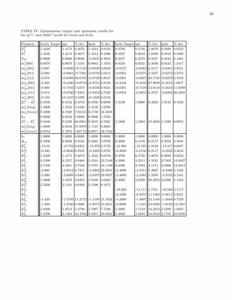
30
TABLE IV: Optimization targets and optimized results forthe sp3s∗ and s3d5s* model for GaAs and InAs.
Property GaAs Target sps % dev spds % dev InAs Target sps % dev spds % dev
EΓg 1.4240 1.4173 0.4676 1.4242 0.0150 0.3700 0.3740 1.0679 0.3699 0.0232
EΓc 1.4240 1.4173 0.4675 1.4212 0.1996 0.5957 0.6019 1.0406 0.5942 0.2496
Vhh 0.0000 0.0000 0.0000 -0.0031 0.3055 0.2257 0.2279 0.2247 0.2243 0.1401
m∗
c [001] 0.0670 0.0679 1.3195 0.0662 1.1353 0.0239 0.0245 2.3030 0.0235 1.5417
m∗
lh[001] -0.087 -0.0699 19.7125 -0.0830 4.6849 -0.0273 -0.0282 3.2117 -0.0281 2.9541
m∗
lh[011] -0.080 -0.0661 17.7381 -0.0759 5.6414 -0.0264 -0.0275 4.3227 -0.0273 3.3575
m∗
lh[111] -0.078 -0.0498 36.6755 -0.0740 5.8547 -0.0261 -0.0207 20.7535 -0.0270 3.5783
m∗
hh[001] -0.403 -0.4436 10.0710 -0.3751 6.9198 -0.3448 -0.4410 27.9049 -0.3516 1.9617
m∗
hh[011] -0.660 -0.7103 7.6270 -0.6538 0.9421 -0.6391 -0.7159 12.0144 -0.5634 11.8389
m∗
hh[111] -0.813 -0.8726 7.3332 -0.8352 2.7329 -0.8764 -0.8972 2.3757 -0.6982 20.3385
m∗
so[001] -0.150 -0.1447 3.5239 -0.1629 8.6134
EXc −EΓ
c 0.4760 0.4742 0.3753 0.4760 0.0099 1.9100 1.9008 0.4829 1.9131 0.1626
m∗
X [long] 1.3000 1.2552 3.4436 1.3138 1.0596
m∗
X [trans] 0.2300 4.1920 1722.61 0.1740 24.3358
kX 0.9000 0.8550 5.0000 0.8860 1.5556
ELc −EΓ
c 0.2840 0.5339 88.0001 0.2825 0.5201 1.1600 1.3394 15.4628 1.1589 0.0915
m∗
L[long] 1.9000 2.9849 57.0979 1.7125 9.8685
m∗
L[trans] 0.0754 1.1972 1487.74 0.0971 28.7342
kL 1.0000 1.0000 0.0000 1.0000 0.0000 1.0000 1.0000 0.0000 1.0000 0.0000
∆so 0.3400 0.3636 6.9545 0.3265 3.9792 0.3800 0.4150 9.2117 0.3932 3.4644
EΓ6v -13.10 -12.703 3.0321 -12.370 5.5723 -12.300 -12.535 1.9149 -13.417 9.0847
E∆so -0.340 -0.3636 6.9545 -0.3265 3.9792 -0.3800 -0.4150 9.2117 -0.3932 3.4644
EΓ
6c 1.4240 1.4173 0.4676 1.4242 0.0150 0.3700 0.3740 1.0679 0.3699 0.0232
EΓ7c 4.5300 4.3557 3.8468 3.4544 23.7449 4.3900 4.3314 1.3342 3.7402 14.8027
EΓ
8c 4.7160 4.5861 2.7546 3.5785 24.1198 4.6300 4.7294 2.1474 4.0466 12.6013
EX6v -2.880 -2.8013 2.7321 -2.2302 22.5631 -2.4000 -2.5311 5.4607 -2.3486 2.1434
EX7v -2.800 -2.6699 4.6481 -2.0470 26.8927 -2.4000 -2.4383 1.5958 -2.2525 6.1441
EX6c 1.9800 1.9278 2.6376 1.9199 3.0363 2.5000 3.2599 30.3955 2.6286 5.1458
EX7c 2.3200 2.1101 9.0469 2.1298 8.1972
EL4v -10.920 -11.111 1.7551 -10.580 3.1117
EL5v -6.2300 -6.9272 11.1903 -5.8611 5.9221
EL6v -1.420 -1.5793 11.2172 -1.1169 21.3432 -1.2000 -1.4897 24.1448 -1.3048 8.7339
EL7v -1.200 -1.2766 6.3866 -0.8975 25.2051 -0.9000 -1.1221 24.6830 -1.0129 12.5407
EL6c 1.8500 1.9513 5.4736 1.7067 7.7440 1.5000 1.7133 14.2213 1.5289 1.9235
EL7c 5.4700 3.1464 42.4786 3.9357 28.0501 5.4000 4.3284 19.8452 4.1758 22.6708

31
-10
-5
0
5
10
y (
nm
)
-10 10x (nm)
-10
-5
0
5
10
y (
nm
)
-10
0
10
y (nm)-10
100
x (nm)
0
5
10
15 x 10-3
|Y(r
)|2
-10
0
10
-10
100
x (nm)
0
5
10
15 x 10-3
-10 10x (nm)
-10
0
10
-10
100
x (nm)
0
5
10
15 x 10-3
-10 10x (nm)
-50
5
-5
0
5
-2
0
2
x (nm)y (nm)
z (
nm
)
-50
5
-5
0
5
-2
0
2
x (nm)y (nm)-5
05
-5
0
5
-2
0
2
x (nm)y (nm)
(a) (b) (c)
(d) (e) (f)
(g) (h) (i)
(j) (k) (l)
E=1.3155eV
∆E=+0.00meVE=1.3169eV
∆E=+1.38meV
FIG. 13: Electron ground state wave functions without dis-order - VCA (first column), and two different random alloyconfigurations (middle and right column). First row: scat-ter plot of wave function in 3-D. Second, third, and fourthrow: colored contour plot, outlined contour and surface plotsliced through the middle of the quantum dot at a constantz, respectively.

32
-50
5
-50
5-2
0
2
x (nm)y (nm)
z (n
m)
-10
-5
0
5
10
y (n
m)
-10 10x (nm)
-10
-5
0
5
10
y (n
m)
-100
10
y (nm)-10
100
x (nm)
0
5
10
15 x 10-3
|Ψ(r
)|2
-100
10
-1010
0x (nm)
0
5
10
15 x 10-3
-10 10x (nm)
-100
10
-1010
0x (nm)
0
5
10
15 x 10-3
-10 10x (nm)
-50
5
-50
5-2
0
2
x (nm)y (nm) -50
5
-50
5-2
0
2
x (nm)y (nm)
(a) (b) (c)
(d) (e) (f)
(g) (h) (i)
(j) (k) (l)
E=0.2208eV∆E=+0.00meV
E=0.2174eV∆E=-3.44meV
FIG. 14: Hole ground state wave functions without disorder -VCA (first column), and two different random alloy configu-rations (middle and right column). First row: scatter plot ofwave function in 3-D. Second, third, and fourth row: coloredcontour plot, outlined contour and surface plot sliced throughthe middle of the quantum dot at a constant z, respectively.

33
-10
-5
0
5
10
y (n
m)
-10 10x (nm)
-10
-5
0
5
10
y (n
m)
-10 10x (nm) -10 10x (nm)
-10
-5
0
5
10
y (n
m)
-10
-5
0
5
10
y (n
m)
(a) electron 1 (b) electron 2 (c) electron 3
(d) electron 4 (e) electron 5 (f) electron 6
(g) hole 1 (h) hole 2 (i) hole 3
(j) hole 4 (k) hole 5 (l) hole 6
E=1.3601eV∆E=0.000meV
E=1.3832eV∆E=+23.1meV
E=1.3843eV∆E=+24.2meV
E=1.4038eV∆E=+43.7meV
E=1.4059eV∆E=+45.8meV
E=1.4063eV∆E=+46.1meV
E=0.2089eV∆E=-0.00meV
E=0.1942eV∆E=-14.7meV
E=0.1928eV∆E=-16.0meV
E=0.1811eV∆E=-27.8meV
E=0.1780eV∆E=-30.9meV
E=0.1765eV∆E=-32.4meV
FIG. 15: Electron and hole wave functions with disorder.

34
1.22 1.225 1.23 1.235 1.240
10
20
30
40
50
Conduction band state (eV)0.18 0.185 0.19 0.195 0.2
0
10
20
30
40
50
60
Valence band state(eV)
Sam
ples
1.02 1.03 1.04 1.050
10
20
30
40
50
Energy gap (eV)
0.595 0.6 0.6050
10
20
30
40
50
In concentration (x)
1.226 1.228 1.23 1.232 1.2340
10
20
30
40
50
Conduction band state (eV)0.184 0.186 0.188 0.19
0
10
20
30
40
50
60
Valence band state (eV)
Sam
ples
1.035 1.04 1.045 1.050
10
20
30
40
50
Energy gap (eV)
E =0.1862eVσ =0.9meVv
v
N=490h=30
E =1.2298eVσ =1.4meVc
c E =1.0436eVσ =2.3meVG
G
E =0.1938eVσ =1.9meVv
v E =1.2291eVσ =2.8meVc
c E =1.0352eVσ =4.5meVG
G
(a)
N=560h=30
(b) (c)
(d) (e) (f)
x =0.6σ =0.0016
0.18 0.19 0.21.22
1.23
1.24
Ev (eV)
Ec
(eV
)
0.595 0.6 0.6051.22
1.23
1.24
In concentration (x)
(g) (h) (i)
Ev (eV)
Ev (eV) Ec (eV)
Ec (eV)
Sam
ples
FIG. 16: First row: histogram distributions of 560 sampleswith 30 samples per bin for the valence band edge (a), conduc-tion band edge (b), and band gap (c) using atomic granularity(AG). Second row: comparison of cell granularity (CG) dis-order results to results in the first row based on 490 samples.(g) scatter plots of Ec versus Ev for all the samples shownin (a-b) and (d-e). Red solid lines indicate least mean squarefit. (h) scatter plot of Ec as a function of actual In concen-tration for cell granularity. (i) histogram on actual In alloyconcentration in the cell granularity.

35
0 0.5 10
0.5
1
1.5
In Concentration
Ene
rgy
(eV
)
0 0.2 0.40.6
0.8
1
1.2
1.4
Ev (eV)
Ec (
eV)
Ec1Ec
Ev
no strainbi-axhydrolocalq-dot
no strainbi-axhydrolocalq-dot
(a) (b)
In=0.6
Ev1
FIG. 17: (a) three sets of conduction and valence bands ofInxGa1−xAs as a function of In concentration x. Dashed line:no strain, solid line: bi-axially strained to GaAs, dotted line:hydrostatically strained to GaAs. Ec1 and Ev1 quantum dotenergy distributions (circles) similar to Figure 16h) with theirlinear regression fits (red lines). Locally averaged conductionand valence band edge inside a quantum dot is indicated witha plus sign. (b) conduction band energies plotted versus cor-responding valence band edges from (a). Squares indicate anIn concentration of 0.6.