Designs for Ultra-Tiny, Special-Purpose Nanoelectronic ...Designs for Ultra-Tiny, Special-Purpose...
13
2528 IEEE TRANSACTIONS ON CIRCUITS AND SYSTEMS—I: REGULAR PAPERS, VOL. 54, NO. 11, NOVEMBER 2007 Designs for Ultra-Tiny, Special-Purpose Nanoelectronic Circuits Shamik Das, Member, IEEE, Alexander J. Gates, Hassen A. Abdu, Student Member, IEEE, Garrett S. Rose, Member, IEEE, Carl A. Picconatto, and James C. Ellenbogen, Member, IEEE Abstract—Designs and simulation results are given for two small, special-purpose nanoelectronic circuits. The area of special-purpose nanoelectronics has not been given much con- sideration previously, though much effort has been devoted to the development of general-purpose nanoelectronic systems, i.e., nanocomputers. This paper demonstrates via simulation that the nanodevices and nanofabrication techniques developed re- cently for general-purpose nanocomputers also might be applied with substantial benefit to implement less complex nanocircuits targeted at specific applications. Nanocircuits considered here are a digital controller for the leg motion on an autonomous millimeter-scale robot and an analog nanocircuit for amplification of signals in a tiny optoelectronic sensor or receiver. Simulations of both nanocircuit designs show significant improvement over microelectronic designs in metrics such as footprint area and power consumption. These improvements are obtained from de- signs employing nanodevices and nanofabrication techniques that already have been demonstrated experimentally. Thus, the results presented here suggest that such improvements might be realized in the near term for important, special-purpose applications. Index Terms—Design methodology, nanocircuit, nanocom- puting, nano-electronics, nanotechnology, simulation. I. INTRODUCTION T HE great progress toward building electronic circuits inte- grated on the nanometer scale [1]–[42] has opened the pos- sibility for shrinking drastically the size and power consump- tion of large-scale, general-purpose electronic memories and pro- cessors. These recent advances in nanofabrication and nanoelec- tronics could have conspicuous, pervasive impacts for general- purpose computing in several years’ time. However, these ad- vances also make it possible to shrink the form factor and power requirements for a wide class of much simpler circuits. Such cir- cuits often are dedicated to specialized applications in the control and monitoring of other systems. They are less conspicuous than the larger general-purpose processors and memories, but even more pervasive. Moreover, the simplicity of these special-pur- pose nanocircuits is such that they might be realized industrially in only a few years, and they might find great use immediately thereafter in shrinking the larger systems in which they are em- Manuscript received February 18, 2007; revised July 4, 2007. This work was supported by the MITRE Technology Program. This paper was recommended by Guest Editor C. Lau. S. Das, A. J. Gates, H. A. Abdu, C. A. Picconatto, and J. C. Ellenbogen are with the Nanosystems Group at The MITRE Corporation, McLean, VA 22102 USA (e-mail: [email protected]). G. Rose is with the Nanosystems Group at The MITRE Corporation, McLean, VA 22102, USA, and also with Polytechnic University, Brooklyn, NY 11201 USA. Digital Object Identifier 10.1109/TCSI.2007.907864 bedded. Thus, it is the design of these simple, special-purpose nanoelectronic circuits that we begin to consider here. Special-purpose nanoelectronic circuits might be employed in a number of applications. For example, one class of these ap- plications is control processing. Nanocircuits for digital control might be used to miniaturize existing applications or enable new ones, such as autonomous microsensors (“smart dust”) [43], medical microrobotics [44]–[46], or other micro/nano electro- mechanical systems. Another class of applications that might benefit from special-purpose nanoelectronics is communica- tions. For example, novel, tiny optical or radio data transceivers might be implemented using analog or mixed-signal nano- electronic circuits. Also, field-programmable nanocircuits could be utilized to implement or store codecs for a compact, flexible software-defined radio system [47], [48]. Finally, as an example bridging these two classes, radio-frequency identification (RFID) systems [49] might be miniaturized or augmented using nanoelectronic information storage, control, or communications. To begin to explore the utility of special-purpose nanoelec- tronic circuits for applications such as these, the authors have designed and simulated two such circuits for use in two ex- ample applications. The first circuit we consider is for digital control of a six-legged, millimeter-scale robot. This nanocircuit is derived from architectures proposed for large-scale nanopro- cessors [27], [51]. As presently designed, this special-purpose nanocircuit will coordinate the motion of the legs of the robot. However, the circuit design is adaptable or extensible to control other functions on the robot. The second nanocircuit design considered here is for an analog nanoelectronic amplifier for use in an optoelectronic communications system. This circuit could be used to imple- ment very-wide-bandwidth optical communications. It also could be embedded in the individual pixels of an optical sensor array, enabling “smart pixel” capabilities [52]. The development of ultra-tiny, ultra-dense circuits such as these will entail overcoming significant challenges. Many of these challenges are inherited from the more complex problem of developing extended, general-purpose nanoelectronic systems. The advanced techniques that have been devised to address those larger challenges likely will be even more effective in over- coming the lower hurdles presented by simpler, special-purpose nanoelectronic circuits. Section II discusses the techniques and devices that have been selected for the designs presented here. Following this discussion, Sections III and IV detail the de- sign and the likely performance of the specific special-purpose digital and analog nanocircuits mentioned above. Section V pro- vides our conclusions based upon these design efforts. 1549-8328/$25.00 © 2007 IEEE
Transcript of Designs for Ultra-Tiny, Special-Purpose Nanoelectronic ...Designs for Ultra-Tiny, Special-Purpose...
2528 IEEE TRANSACTIONS ON CIRCUITS AND SYSTEMS—I: REGULAR PAPERS, VOL. 54, NO. 11, NOVEMBER 2007
Designs for Ultra-Tiny, Special-PurposeNanoelectronic Circuits
Shamik Das, Member, IEEE, Alexander J. Gates, Hassen A. Abdu, Student Member, IEEE,Garrett S. Rose, Member, IEEE, Carl A. Picconatto, and James C. Ellenbogen, Member, IEEE
Abstract—Designs and simulation results are given for twosmall, special-purpose nanoelectronic circuits. The area ofspecial-purpose nanoelectronics has not been given much con-sideration previously, though much effort has been devoted tothe development of general-purpose nanoelectronic systems, i.e.,nanocomputers. This paper demonstrates via simulation thatthe nanodevices and nanofabrication techniques developed re-cently for general-purpose nanocomputers also might be appliedwith substantial benefit to implement less complex nanocircuitstargeted at specific applications. Nanocircuits considered hereare a digital controller for the leg motion on an autonomousmillimeter-scale robot and an analog nanocircuit for amplificationof signals in a tiny optoelectronic sensor or receiver. Simulationsof both nanocircuit designs show significant improvement overmicroelectronic designs in metrics such as footprint area andpower consumption. These improvements are obtained from de-signs employing nanodevices and nanofabrication techniques thatalready have been demonstrated experimentally. Thus, the resultspresented here suggest that such improvements might be realizedin the near term for important, special-purpose applications.
Index Terms—Design methodology, nanocircuit, nanocom-puting, nano-electronics, nanotechnology, simulation.
I. INTRODUCTION
THE great progress toward building electronic circuits inte-grated on the nanometer scale [1]–[42] has opened the pos-
sibility for shrinking drastically the size and power consump-tionof large-scale,general-purposeelectronicmemoriesandpro-cessors. These recent advances in nanofabrication and nanoelec-tronics could have conspicuous, pervasive impacts for general-purpose computing in several years’ time. However, these ad-vances also make it possible to shrink the form factor and powerrequirements for a wide class of much simpler circuits. Such cir-cuits often are dedicated to specialized applications in the controland monitoring of other systems. They are less conspicuous thanthe larger general-purpose processors and memories, but evenmore pervasive. Moreover, the simplicity of these special-pur-pose nanocircuits is such that they might be realized industriallyin only a few years, and they might find great use immediatelythereafter in shrinking the larger systems in which they are em-
Manuscript received February 18, 2007; revised July 4, 2007. This work wassupported by the MITRE Technology Program. This paper was recommendedby Guest Editor C. Lau.
S. Das, A. J. Gates, H. A. Abdu, C. A. Picconatto, and J. C. Ellenbogen arewith the Nanosystems Group at The MITRE Corporation, McLean, VA 22102USA (e-mail: [email protected]).
G. Rose is with the Nanosystems Group at The MITRE Corporation, McLean,VA 22102, USA, and also with Polytechnic University, Brooklyn, NY 11201USA.
Digital Object Identifier 10.1109/TCSI.2007.907864
bedded. Thus, it is the design of these simple, special-purposenanoelectronic circuits that we begin to consider here.
Special-purpose nanoelectronic circuits might be employedin a number of applications. For example, one class of these ap-plications is control processing. Nanocircuits for digital controlmight be used to miniaturize existing applications or enable newones, such as autonomous microsensors (“smart dust”) [43],medical microrobotics [44]–[46], or other micro/nano electro-mechanical systems. Another class of applications that mightbenefit from special-purpose nanoelectronics is communica-tions. For example, novel, tiny optical or radio data transceiversmight be implemented using analog or mixed-signal nano-electronic circuits. Also, field-programmable nanocircuitscould be utilized to implement or store codecs for a compact,flexible software-defined radio system [47], [48]. Finally,as an example bridging these two classes, radio-frequencyidentification (RFID) systems [49] might be miniaturized oraugmented using nanoelectronic information storage, control,or communications.
To begin to explore the utility of special-purpose nanoelec-tronic circuits for applications such as these, the authors havedesigned and simulated two such circuits for use in two ex-ample applications. The first circuit we consider is for digitalcontrol of a six-legged, millimeter-scale robot. This nanocircuitis derived from architectures proposed for large-scale nanopro-cessors [27], [51]. As presently designed, this special-purposenanocircuit will coordinate the motion of the legs of the robot.However, the circuit design is adaptable or extensible to controlother functions on the robot.
The second nanocircuit design considered here is for ananalog nanoelectronic amplifier for use in an optoelectroniccommunications system. This circuit could be used to imple-ment very-wide-bandwidth optical communications. It alsocould be embedded in the individual pixels of an optical sensorarray, enabling “smart pixel” capabilities [52].
The development of ultra-tiny, ultra-dense circuits such asthese will entail overcoming significant challenges. Many ofthese challenges are inherited from the more complex problem ofdeveloping extended, general-purpose nanoelectronic systems.The advanced techniques that have been devised to address thoselarger challenges likely will be even more effective in over-coming the lower hurdles presented by simpler, special-purposenanoelectronic circuits. Section II discusses the techniques anddevices that have been selected for the designs presented here.
Following this discussion, Sections III and IV detail the de-sign and the likely performance of the specific special-purposedigital and analog nanocircuits mentioned above. Section V pro-vides our conclusions based upon these design efforts.
1549-8328/$25.00 © 2007 IEEE
mastro
Text Box
Approved for Public Release; Distribution Unlimited Case # 07-1029
DAS et al.: DESIGNS FOR ULTRA-TINY, SPECIAL-PURPOSE NANOELECTRONIC CIRCUITS 2529
II. NANODEVICES AND NANOFABRICATION FOR
SPECIAL-PURPOSE NANOELECTRONIC CIRCUITS
A number of novel nanoelectronic devices have been devel-oped in the pursuit of extended nanocomputer systems. Suchnanodevices exhibit a wide variety of electronic behaviors.These include classical behaviors such as Ohmic resistanceat low voltage [8] and rectification [53]–[55]. Less commonbehaviors also have been demonstrated, such as negative differ-ential resistance [13], Coulomb blockade [56], and hystereticswitching [54].
Furthermore, devices such as nanotransistors [10], [11], [14],[57] and molecular switches [5]–[8], [12], [58] have been incor-porated into prototypes of small circuits, such as individual logicgates, as well as extended systems. In particular, effective use ofsuch devices has been demonstrated in prototypes of extendednanomemory systems integrated on the molecular scale [34],[38], [40], [41]. As a result, methods now exist for fabricatingsystems composed of hundreds of thousands of nanodevices.Successful refinement of these methods should permit the fab-rication of systems containing the many billions of devices thatwill be required in a nanocomputer system. In the interim, thefabrication of smaller, simpler circuits consisting of only tens orhundreds of devices should be feasible.
In addition to the demonstrated prototype systems citedabove, a large number of proposals have been put forth forsystem architectures that would integrate one or more of thevarious molecular-scale devices demonstrated to date [24],[27], [28], [30]–[33], [35]–[37], [39]. All of these proposalsand demonstrations are based upon a nanoelectronic systemarchitecture termed the crossbar array [25], [29], which callsfor the homogeneous distribution of nanodevices within tiledarrays of crossed nanowires.
The primary reason for making this design decision is thatthe fabrication of arbitrary, heterogeneous extended structuresat the nanoscale remains a significant unsolved problem [59].At larger length scales with lower densities, this capability istaken for granted, because at such scales, optical lithography iscapable of precise patterning. At the molecular scale, of the sev-eral methods of integration that have been devised, the majorityproduce homogeneous nanowire crossbar arrays [60]–[64].
Just using such simple crossbar structures, however, it shouldbe feasible to develop small, special-purpose nanoelectronic cir-cuits. Thus, the circuits presented in the following sections aresuitable for nanofabrication using established methods, such asnanoimprinting, and using demonstrated nanodevices, such assemiconducting nanowire transistors. The circuits also are suf-ficiently simple to avoid many of the challenges [59] faced inthe development of extended nanoelectronic systems. The fol-lowing sections of this paper will elucidate how nanocircuitssimple enough to ease fabrication also can be sufficiently com-plex to carry out useful functions.
III. DESIGN AND ANALYSIS OF A SPECIAL-PURPOSE
DIGITAL NANOCIRCUIT: CONTROL NANOCIRCUIT FOR A
MILLIMETER-SCALE AUTONOMOUS ROBOT
A. Overview
Using the nanowire-based structures discussed in the pre-vious section, we consider here the design of a portion of a dig-
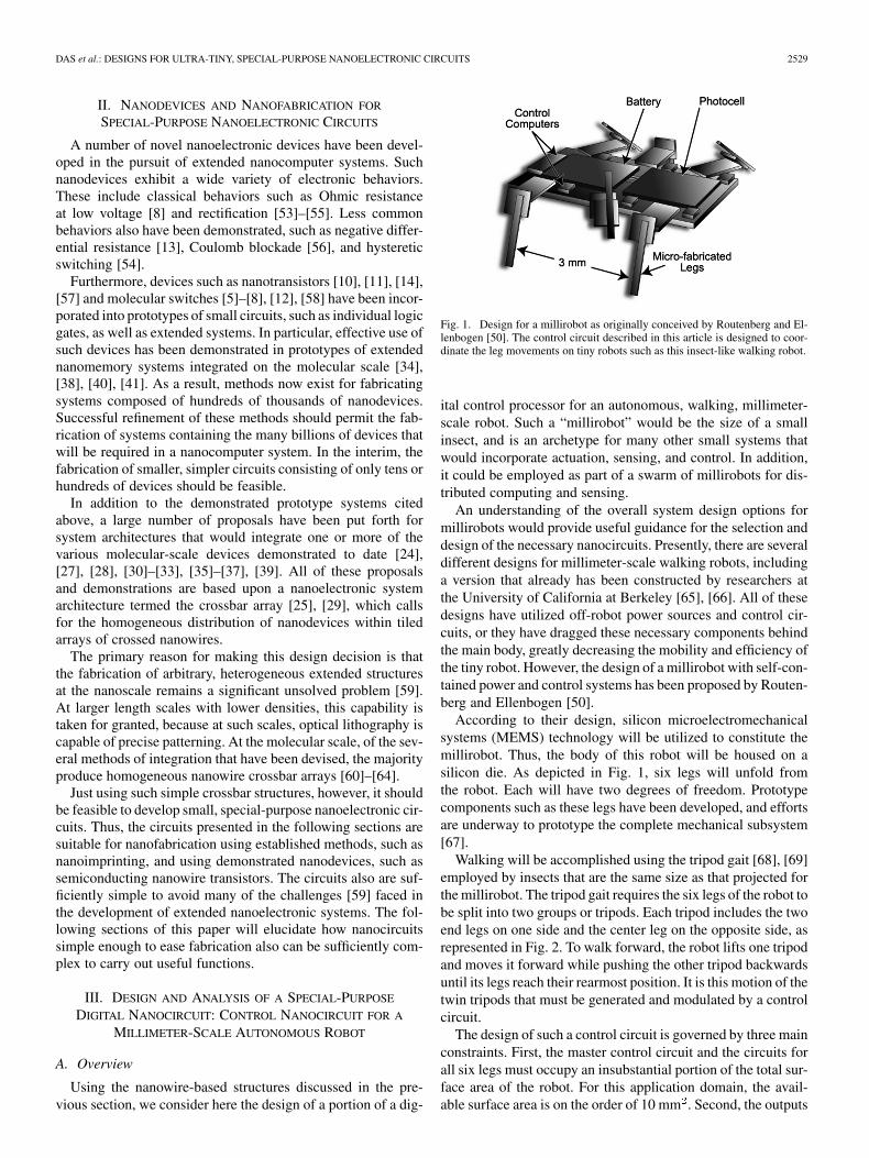
Fig. 1. Design for a millirobot as originally conceived by Routenberg and El-lenbogen [50]. The control circuit described in this article is designed to coor-dinate the leg movements on tiny robots such as this insect-like walking robot.
ital control processor for an autonomous, walking, millimeter-scale robot. Such a “millirobot” would be the size of a smallinsect, and is an archetype for many other small systems thatwould incorporate actuation, sensing, and control. In addition,it could be employed as part of a swarm of millirobots for dis-tributed computing and sensing.
An understanding of the overall system design options formillirobots would provide useful guidance for the selection anddesign of the necessary nanocircuits. Presently, there are severaldifferent designs for millimeter-scale walking robots, includinga version that already has been constructed by researchers atthe University of California at Berkeley [65], [66]. All of thesedesigns have utilized off-robot power sources and control cir-cuits, or they have dragged these necessary components behindthe main body, greatly decreasing the mobility and efficiency ofthe tiny robot. However, the design of a millirobot with self-con-tained power and control systems has been proposed by Routen-berg and Ellenbogen [50].
According to their design, silicon microelectromechanicalsystems (MEMS) technology will be utilized to constitute themillirobot. Thus, the body of this robot will be housed on asilicon die. As depicted in Fig. 1, six legs will unfold fromthe robot. Each will have two degrees of freedom. Prototypecomponents such as these legs have been developed, and effortsare underway to prototype the complete mechanical subsystem[67].
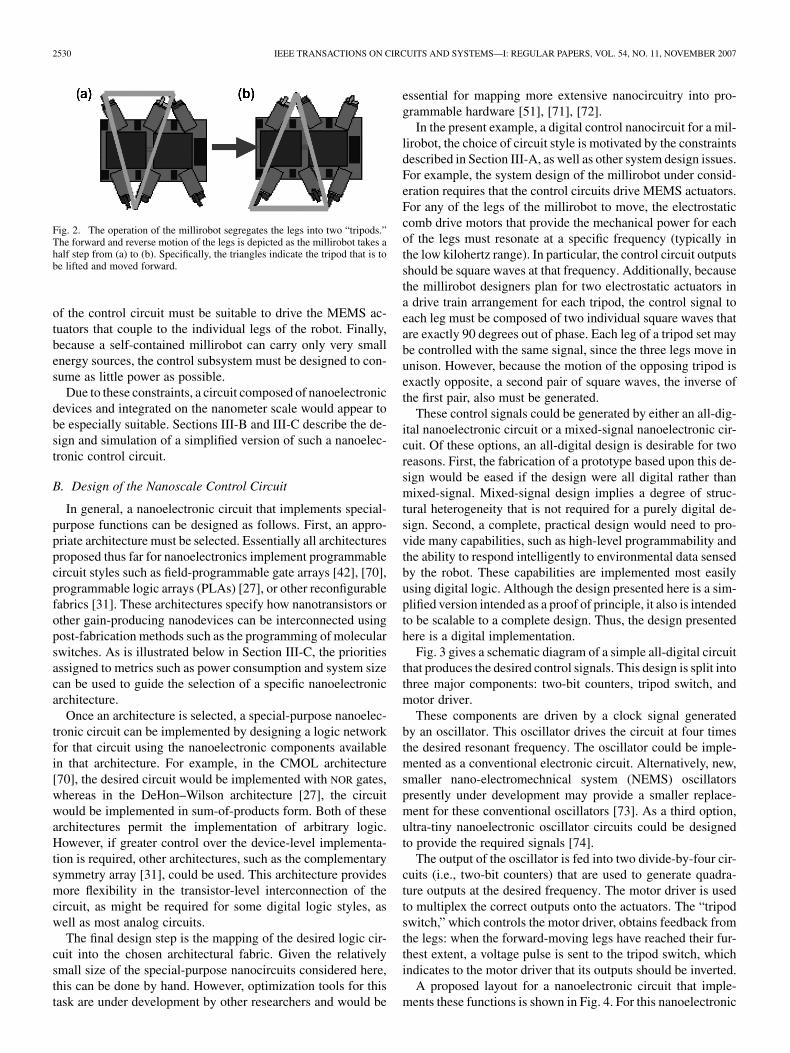
Walking will be accomplished using the tripod gait [68], [69]employed by insects that are the same size as that projected forthe millirobot. The tripod gait requires the six legs of the robot tobe split into two groups or tripods. Each tripod includes the twoend legs on one side and the center leg on the opposite side, asrepresented in Fig. 2. To walk forward, the robot lifts one tripodand moves it forward while pushing the other tripod backwardsuntil its legs reach their rearmost position. It is this motion of thetwin tripods that must be generated and modulated by a controlcircuit.
The design of such a control circuit is governed by three mainconstraints. First, the master control circuit and the circuits forall six legs must occupy an insubstantial portion of the total sur-face area of the robot. For this application domain, the avail-able surface area is on the order of 10 mm . Second, the outputs
2530 IEEE TRANSACTIONS ON CIRCUITS AND SYSTEMS—I: REGULAR PAPERS, VOL. 54, NO. 11, NOVEMBER 2007
Fig. 2. The operation of the millirobot segregates the legs into two “tripods.”The forward and reverse motion of the legs is depicted as the millirobot takes ahalf step from (a) to (b). Specifically, the triangles indicate the tripod that is tobe lifted and moved forward.
of the control circuit must be suitable to drive the MEMS ac-tuators that couple to the individual legs of the robot. Finally,because a self-contained millirobot can carry only very smallenergy sources, the control subsystem must be designed to con-sume as little power as possible.
Due to these constraints, a circuit composed of nanoelectronicdevices and integrated on the nanometer scale would appear tobe especially suitable. Sections III-B and III-C describe the de-sign and simulation of a simplified version of such a nanoelec-tronic control circuit.
B. Design of the Nanoscale Control Circuit
In general, a nanoelectronic circuit that implements special-purpose functions can be designed as follows. First, an appro-priate architecture must be selected. Essentially all architecturesproposed thus far for nanoelectronics implement programmablecircuit styles such as field-programmable gate arrays [42], [70],programmable logic arrays (PLAs) [27], or other reconfigurablefabrics [31]. These architectures specify how nanotransistors orother gain-producing nanodevices can be interconnected usingpost-fabrication methods such as the programming of molecularswitches. As is illustrated below in Section III-C, the prioritiesassigned to metrics such as power consumption and system sizecan be used to guide the selection of a specific nanoelectronicarchitecture.
Once an architecture is selected, a special-purpose nanoelec-tronic circuit can be implemented by designing a logic networkfor that circuit using the nanoelectronic components availablein that architecture. For example, in the CMOL architecture[70], the desired circuit would be implemented with NOR gates,whereas in the DeHon–Wilson architecture [27], the circuitwould be implemented in sum-of-products form. Both of thesearchitectures permit the implementation of arbitrary logic.However, if greater control over the device-level implementa-tion is required, other architectures, such as the complementarysymmetry array [31], could be used. This architecture providesmore flexibility in the transistor-level interconnection of thecircuit, as might be required for some digital logic styles, aswell as most analog circuits.
The final design step is the mapping of the desired logic cir-cuit into the chosen architectural fabric. Given the relativelysmall size of the special-purpose nanocircuits considered here,this can be done by hand. However, optimization tools for thistask are under development by other researchers and would be
essential for mapping more extensive nanocircuitry into pro-grammable hardware [51], [71], [72].
In the present example, a digital control nanocircuit for a mil-lirobot, the choice of circuit style is motivated by the constraintsdescribed in Section III-A, as well as other system design issues.For example, the system design of the millirobot under consid-eration requires that the control circuits drive MEMS actuators.For any of the legs of the millirobot to move, the electrostaticcomb drive motors that provide the mechanical power for eachof the legs must resonate at a specific frequency (typically inthe low kilohertz range). In particular, the control circuit outputsshould be square waves at that frequency. Additionally, becausethe millirobot designers plan for two electrostatic actuators ina drive train arrangement for each tripod, the control signal toeach leg must be composed of two individual square waves thatare exactly 90 degrees out of phase. Each leg of a tripod set maybe controlled with the same signal, since the three legs move inunison. However, because the motion of the opposing tripod isexactly opposite, a second pair of square waves, the inverse ofthe first pair, also must be generated.
These control signals could be generated by either an all-dig-ital nanoelectronic circuit or a mixed-signal nanoelectronic cir-cuit. Of these options, an all-digital design is desirable for tworeasons. First, the fabrication of a prototype based upon this de-sign would be eased if the design were all digital rather thanmixed-signal. Mixed-signal design implies a degree of struc-tural heterogeneity that is not required for a purely digital de-sign. Second, a complete, practical design would need to pro-vide many capabilities, such as high-level programmability andthe ability to respond intelligently to environmental data sensedby the robot. These capabilities are implemented most easilyusing digital logic. Although the design presented here is a sim-plified version intended as a proof of principle, it also is intendedto be scalable to a complete design. Thus, the design presentedhere is a digital implementation.
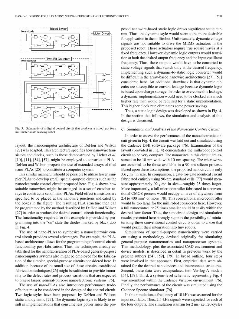
Fig. 3 gives a schematic diagram of a simple all-digital circuitthat produces the desired control signals. This design is split intothree major components: two-bit counters, tripod switch, andmotor driver.
These components are driven by a clock signal generatedby an oscillator. This oscillator drives the circuit at four timesthe desired resonant frequency. The oscillator could be imple-mented as a conventional electronic circuit. Alternatively, new,smaller nano-electromechnical system (NEMS) oscillatorspresently under development may provide a smaller replace-ment for these conventional oscillators [73]. As a third option,ultra-tiny nanoelectronic oscillator circuits could be designedto provide the required signals [74].
The output of the oscillator is fed into two divide-by-four cir-cuits (i.e., two-bit counters) that are used to generate quadra-ture outputs at the desired frequency. The motor driver is usedto multiplex the correct outputs onto the actuators. The “tripodswitch,” which controls the motor driver, obtains feedback fromthe legs: when the forward-moving legs have reached their fur-thest extent, a voltage pulse is sent to the tripod switch, whichindicates to the motor driver that its outputs should be inverted.
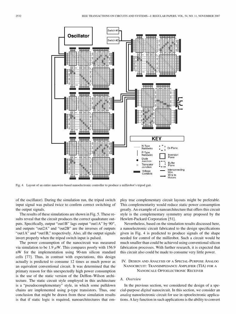
A proposed layout for a nanoelectronic circuit that imple-ments these functions is shown in Fig. 4. For this nanoelectronic
DAS et al.: DESIGNS FOR ULTRA-TINY, SPECIAL-PURPOSE NANOELECTRONIC CIRCUITS 2531
Fig. 3. Schematic of a digital control circuit that produces a tripod gait for amillimeter-scale walking robot.
layout, the nanocomputer architecture of DeHon and Wilson[27] was adapted. This architecture specifies how nanowire tran-sistors and diodes, such as those demonstrated by Lieber et al.[10], [11], [54], [57], might be employed to construct a PLA .DeHon and Wilson propose the use of extended arrays of tilednano-PLAs [25] to constitute a computer system.
In a similar manner, it should be possible to utilize fewer, sim-pler PLAs to develop small, special-purpose circuits such as thenanoelectronic control circuit proposed here. Fig. 4 shows howsuitable nanowires might be arranged in a set of crossbar ar-rays to construct a set of nano-PLAs. Field-effect transistors arespecified to be placed at the nanowire junctions indicated bythe boxes in the figure. The resulting PLA structure then canbe programmed by the method described by DeHon and Wilson[27] in order to produce the desired control-circuit functionality.The functionality required for this example is provided by pro-gramming into the “on” state the diodes marked by black dotsin Fig. 4.
The use of nano-PLAs to synthesize a nanoelectronic con-trol circuit provides several advantages. For example, the PLA-based architecture allows for the programming of control-circuitfunctionality post-fabrication. Thus, the techniques already es-tablished for the nanofabrication of PLA-based general-purposenanocomputer systems also might be employed for the fabrica-tion of the simpler, special-purpose circuits considered here. Inaddition, because of the small size of these circuits, establishedfabrication techniques [26] might be sufficient to provide immu-nity to the defect rates and process variations that are expectedto plague larger, general-purpose nanoelectronic systems [75].
The use of nano-PLAs also introduces performance trade-offs that must be considered in the design of the control circuit.Two logic styles have been proposed by DeHon and Wilson:static and dynamic [27]. The dynamic logic style is likely to re-sult in implementations that consume less power since the pro-
posed nanowire-based static logic draws significant static cur-rent. Thus, the dynamic style would seem to be more desirablefor application in the millirobot. Unfortunately, dynamic voltagesignals are not suitable to drive the MEMS actuators in theproposed robot. These actuators require true square waves at afixed frequency. However, dynamic logic outputs would transi-tion at both the desired output frequency and the input oscillatorfrequency. Thus, these outputs would have to be converted tostatic voltage signals that switch only at the desired frequency.Implementing such a dynamic-to-static logic converter wouldbe difficult in the array-based nanowire architectures [27], [51]considered here. An additional drawback is that dynamic cir-cuits are susceptible to current leakage because dynamic logicis based upon charge storage. In order to overcome this leakage,a dynamic implementation would need to be clocked at a muchhigher rate than would be required for a static implementation.This higher clock rate eliminates some power savings.
Thus, a static logic design was developed as shown in Fig. 4.In the section that follows, the simulation and analysis of thisdesign is discussed.
C. Simulation and Analysis of the Nanoscale Control Circuit
In order to assess the performance of the nanoelectronic cir-cuit given in Fig. 4, the circuit was laid out and simulated usingthe Cadence DFII software package [76]. Examination of thelayout (provided in Fig. 4) demonstrates the millirobot controlcircuit to be very compact. The nanowires in this circuit are as-sumed to be 10-nm wide with 10-nm spacing. The microwiresare assumed to be those available in a 90-nm silicon process.Based upon these assumptions, the proposed nanocircuit is only3.6 m in size. In comparison, a gate-for-gate identical circuitfabricated entirely using 90-nm standard cells [77] would mea-sure approximately 92 m in size—roughly 25 times larger.More importantly, a full microcontroller fabricated in a conven-tional CMOS process would occupy an area of anywhere from2.4 to 400 mm or more [78]. This conventional microcontrollerwould be too large for the millirobot considered here. However,a full nanocontroller 25 times smaller could fit easily within thedesired form factor. Thus, the nanocircuit design and simulationresults presented here strongly support the possibility of minia-turizing these conventional control circuits down to a size thatwould permit their integration into tiny robots.
Simulations of special-purpose nanocircuitry were carriedout using a methodology devised originally for simulatinggeneral-purpose nanomemories and nanoprocessor systems.This methodology, plus the associated CAD environment anddevice models, is described in detail in previous work by thepresent authors [54], [59], [79]. In broad outline, four stepswere involved in that approach. First, empirical data were ob-tained for the desired nanodevices and interconnect structures.Second, these data were encapsulated into Verilog-A models[54], [59]. Third, a system-level schematic representing Fig. 4was assembled within the Cadence Virtuoso environment [76].Finally, the performance of the circuit was simulated using theCadence Spectre simulator [76].
In this simulation, a frequency of 10 kHz was assumed for theinput oscillator. Thus, 2.5-kHz signals were expected for each ofthe four outputs. The simulation was run for 2 ms (i.e., 20 cycles
2532 IEEE TRANSACTIONS ON CIRCUITS AND SYSTEMS—I: REGULAR PAPERS, VOL. 54, NO. 11, NOVEMBER 2007
Fig. 4. Layout of an entire nanowire-based nanoelectronic controller to produce a millirobot’s tripod gait.
of the oscillator). During the simulation run, the tripod switchinput signal was pulsed twice to confirm correct switching ofthe output signals.
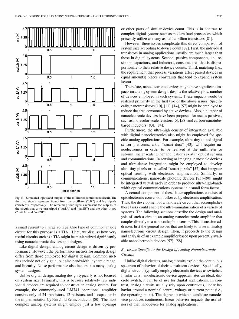
The results of these simulations are shown in Fig. 5. These re-sults reveal that the circuit produces the correct quadrature out-puts. Specifically, output “out1B” lags output “out1A” by 90 ,and outputs “out2A” and “out2B” are the inverses of outputs“out1A” and “out1B,” respectively. Also, all the output signalsinvert properly when the tripod switch input is pulsed.
The power consumption of the nanocircuit was measuredvia simulation to be 1.9 W. This compares poorly with 156.9nW for the implementation using 90-nm silicon standardcells [77]. Thus, in contrast with expectations, this designactually is predicted to consume 12 times as much power asan equivalent conventional circuit. It was determined that theprimary reason for this unexpectedly high power consumptionis the use of the static version of the DeHon–Wilson archi-tecture. The static circuit style employed in this architectureis a “pseudocomplementary” style, in which some pulldownchains are implemented using p-type transistors. Thus, oneconclusion that might be drawn from these simulation resultsis that if static logic is required, nanoarchitectures that em-
ploy true complementary circuit layouts might be preferable.This complementarity would reduce static power consumptiongreatly. An example of a nanoarchitecture that offers this circuitstyle is the complementary symmetry array proposed by theHewlett-Packard Corporation [51].
Nevertheless, based on the simulation results discussed here,a nanoelectronic circuit fabricated to the design specificationsgiven in Fig. 4 is predicted to produce signals of the shapeneeded for control of the millirobot. Such a circuit would bemuch smaller than could be achieved using conventional siliconfabrication processes. With further research, it is expected thatthis circuit also could be made to consume very little power.
IV. DESIGN AND ANALYSIS OF A SPECIAL-PURPOSE ANALOG
NANOCIRCUIT: TRANSIMPEDANCE AMPLIFIER (TIA) FOR A
NANOSCALE OPTOELECTRONIC RECEIVER
A. Overview
In the previous section, we considered the design of a spe-cial-purpose digital nanocircuit. In this section, we consider ananalog nanoelectronic circuit for use in optoelectronic applica-tions. A key function in such applications is the ability to convert
DAS et al.: DESIGNS FOR ULTRA-TINY, SPECIAL-PURPOSE NANOELECTRONIC CIRCUITS 2533
Fig. 5. Simulated inputs and outputs of the millirobot control nanocircuit. Thefirst two signals represent inputs from the oscillator (“clk”) and leg tripods(“switch”), respectively. The remaining four signals represent the outputs ofthe circuit that drive one tripod (“out1A” and “out1B”) and the other tripod(“out2A” and “out2B”).
a small current to a large voltage. One type of common analogcircuit for this purpose is a TIA . Here, we discuss how veryuseful circuits such as a TIA might be miniaturized significantlyusing nanoelectronic devices and designs.
Like digital design, analog circuit design is driven by per-formance. However, the performance metrics for analog designdiffer from those employed for digital design. Common met-rics include not only gain, but also bandwidth, dynamic range,and linearity. Noise performance also factors into many analogsystem designs.
Unlike digital design, analog design typically is not focusedon system size. Primarily, this is because relatively few indi-vidual devices are required to construct an analog system. Forexample, the commonly-used LM741 operational amplifierconsists only of 24 transistors, 12 resistors, and 1 capacitor inthe implementation by Fairchild Semiconductor [80]. The mostcomplex analog systems might employ just a few op-amps
or other parts of similar device count. This is in contrast tocomplex digital systems such as modern Intel processors, whichpresently utilize as many as half a billion transistors [81].
However, three issues complicate this direct comparison ofsystem size according to device count [82]. First, the individualtransistors in analog applications usually are much larger thanthose in digital systems. Second, passive components, i.e., re-sistors, capacitors, and inductors, consume area that is dispro-portionate to their relative device counts. Third, matching (i.e.,the requirement that process variations affect paired devices inequal amounts) places constraints that tend to expand systemlayout.
Therefore, nanoelectronic devices might have significant im-pacts on analog system design, despite the relatively low numberof devices employed in such systems. These impacts would berealized primarily in the first two of the above issues. Specifi-cally, nanotransistors [10], [11], [14], [57] might be employed toreduce the area consumed by active devices. Also, a number ofnanoelectronic devices have been proposed for use as passives,such as molecular-scale resistors [5], [58] and carbon-nanotube-based inductors [83], [84].
Furthermore, the ultra-high density of integration availablewith digital nanoelectronics also might be employed for spe-cific analog applications. For example, ultra-tiny mixed-signalsensor platforms, a.k.a. “smart dust” [43], will require na-noelectronics in order to be realized at the millimeter orsub-millimeter scale. Other applications exist in optical sensingand communications. In sensing or imaging, nanoscale devicesand ultra-dense integration might be employed to developultra-tiny pixels or so-called “smart pixels” [52] that integrateoptical sensing with electronic amplification. Similarly, incommunications, nanoscale photonic devices [85]–[90] mightbe integrated very densely in order to produce ultra-high-band-width optical communications systems in a small form factor.
A central component of these latter applications consists ofoptoelectronic conversion followed by electronic amplification.Thus, the development of a nanoscale circuit that accomplishesthese tasks could enable the ultra-miniaturization of a variety ofsystems. The following sections describe the design and anal-ysis of such a circuit, an analog nanoelectronic amplifier thatcouples directly to a nanoscale photosensor. This discussion ad-dresses first the general issues that are likely to arise in analognanoelectronic circuit design. Then, it proceeds to the designand analysis of an example amplifier based upon presently avail-able nanoelectronic devices [57], [58].
B. Issues Specific to the Design of Analog NanoelectronicCircuits
Unlike digital circuits, analog circuits exploit the continuousspectrum of behavior of their constituent devices. Specifically,digital circuits typically employ electronic devices as switches.Insofar as a nanoelectronic device approximates an ideal, dis-crete switch, it can be of use for digital applications. In con-trast, analog circuits usually rely upon continuous, linear be-havior around a nominal central voltage or current point (i.e.,the operating point). The degree to which a candidate nanode-vice produces continuous, linear behavior impacts the useful-ness of that nanodevice for analog applications.
2534 IEEE TRANSACTIONS ON CIRCUITS AND SYSTEMS—I: REGULAR PAPERS, VOL. 54, NO. 11, NOVEMBER 2007
Thus, while a variety of devices have been proposed foruse in digital nanoelectronic applications, only a subset ofthese devices is appropriate for analog circuits. For example,Coulomb blockade devices such as single-electron transistors[56] or quantum-dot cellular automata [91], [92] are unlikely tobe suitable, due to their characteristic stair-step current-voltagebehavior. On the other hand, nanotransistors [10], [11], [14],[57] are highly suitable since their behavior is essentially thatof conventional transistors.
However, the behavior of presently-available nanotransistorsdoes depart in some ways from that of conventional transistors.It is expected [11] that as development of such nanodevices ma-tures, these present limitations will be overcome. In the interim,it is useful to consider how these limitations might affect the de-sign and performance of analog nanoelectronic systems.
Present limitations to nanotransistor behavior occur in twoareas, gain and bandwidth. Both of these limitations arise fromthe transistor transconductance, . In presently availablenanodevices, the transconductance may be orders of magni-tude lower than is achievable with conventional transistors[11], [93]. This directly limits the gain that can be producedby nanoelectronic devices and small analog nanoelectroniccircuits. The bandwidth of individual transistors is dictated bythe transition frequency, . For field-effect transistors, this isgiven approximately by
(1)
where and are the coupling capacitances from the tran-sistor gate to the source and drain respectively [94]. In nanotran-sistors, the lower results in a reduced transition frequency,despite the reduced and . As a result, the bandwidth ofanalog nanoelectronic systems is impacted adversely, as well.
In addition to limitations in nanotransistor performance,there exist challenges arising from the use of nanoscale pas-sives. For example, due to the impedance scaling that occurs asdevice dimensions shrink, moderately sized resistors, e.g., lessthan 1 M , would be difficult to fabricate using known nanode-vices or nanoscale interconnects. Similarly, large capacitances,e.g., more than 1 fF, also would be difficult to obtain withoutundermining the intent to ultra-miniaturize. For these reasons,nanocircuit frequency compensation is made difficult, since theprimary methods of compensating integrated circuits involvethe use of resistors and capacitors with specifically tailoredvalues.
Beyond the performance of the active and passive devicesthat constitute analog circuits, the impact of parasitic elementsalso presents a challenge for analog nanoelectronic circuit de-sign. For example, the parasitic resistance of interconnects isaffected adversely by the shrinking of the wire cross-sectionalareas. Thus, as is the case with state-of-the-art microelectronicanalog design, the first-pass design of analog nanoelectronic cir-cuits also must consider parasitic elements together with the in-tended devices.
Finally, as indicated in Section II, it will be difficult tofabricate arbitrary circuit topologies at the nanometer scale.Instead, nanoelectronic circuits must be designed so that they
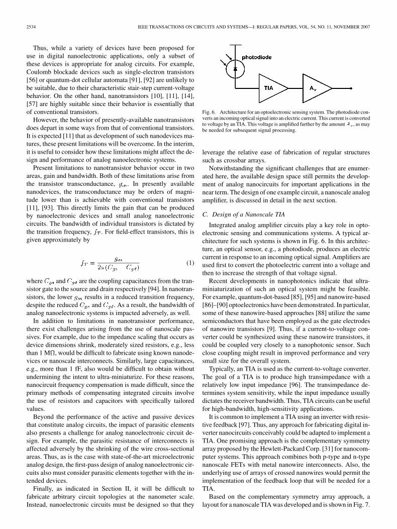
Fig. 6. Architecture for an optoelectronic sensing system. The photodiode con-verts an incoming optical signal into an electric current. This current is convertedto voltage by an TIA. This voltage is amplified further by the amountA , as maybe needed for subsequent signal processing.
leverage the relative ease of fabrication of regular structuressuch as crossbar arrays.
Notwithstanding the significant challenges that are enumer-ated here, the available design space still permits the develop-ment of analog nanocircuits for important applications in thenear term. The design of one example circuit, a nanoscale analogamplifier, is discussed in detail in the next section.
C. Design of a Nanoscale TIA
Integrated analog amplifier circuits play a key role in opto-electronic sensing and communications systems. A typical ar-chitecture for such systems is shown in Fig. 6. In this architec-ture, an optical sensor, e.g., a photodiode, produces an electriccurrent in response to an incoming optical signal. Amplifiers areused first to convert the photoelectric current into a voltage andthen to increase the strength of that voltage signal.
Recent developments in nanophotonics indicate that ultra-miniaturization of such an optical system might be feasible.For example, quantum-dot-based [85], [95] and nanowire-based[86]–[90] optoelectronics have been demonstrated. In particular,some of these nanowire-based approaches [88] utilize the samesemiconductors that have been employed as the gate electrodesof nanowire transistors [9]. Thus, if a current-to-voltage con-verter could be synthesized using these nanowire transistors, itcould be coupled very closely to a nanophotonic sensor. Suchclose coupling might result in improved performance and verysmall size for the overall system.
Typically, an TIA is used as the current-to-voltage converter.The goal of a TIA is to produce high transimpedance with arelatively low input impedance [96]. The transimpedance de-termines system sensitivity, while the input impedance usuallydictates the receiver bandwidth. Thus, TIA circuits can be usefulfor high-bandwidth, high-sensitivity applications.
It is common to implement a TIA using an inverter with resis-tive feedback [97]. Thus, any approach for fabricating digital in-verter nanocircuits conceivably could be adapted to implement aTIA. One promising approach is the complementary symmetryarray proposed by the Hewlett-Packard Corp. [31] for nanocom-puter systems. This approach combines both p-type and n-typenanoscale FETs with metal nanowire interconnects. Also, theunderlying use of arrays of crossed nanowires would permit theimplementation of the feedback loop that will be needed for aTIA.
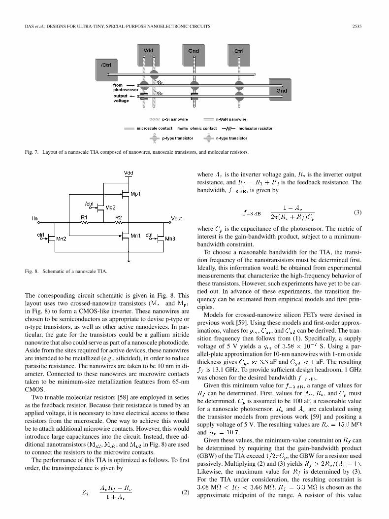
Based on the complementary symmetry array approach, alayout for a nanoscale TIA was developed and is shown in Fig. 7.
DAS et al.: DESIGNS FOR ULTRA-TINY, SPECIAL-PURPOSE NANOELECTRONIC CIRCUITS 2535
Fig. 7. Layout of a nanoscale TIA composed of nanowires, nanoscale transistors, and molecular resistors.
Fig. 8. Schematic of a nanoscale TIA.
The corresponding circuit schematic is given in Fig. 8. Thislayout uses two crossed-nanowire transistors ( andin Fig. 8) to form a CMOS-like inverter. These nanowires arechosen to be semiconductors as appropriate to devise p-type orn-type transistors, as well as other active nanodevices. In par-ticular, the gate for the transistors could be a gallium nitridenanowire that also could serve as part of a nanoscale photodiode.Aside from the sites required for active devices, these nanowiresare intended to be metallized (e.g., silicided), in order to reduceparasitic resistance. The nanowires are taken to be 10 nm in di-ameter. Connected to these nanowires are microwire contactstaken to be minimum-size metallization features from 65-nmCMOS.
Two tunable molecular resistors [58] are employed in seriesas the feedback resistor. Because their resistance is tuned by anapplied voltage, it is necessary to have electrical access to theseresistors from the microscale. One way to achieve this wouldbe to attach additional microwire contacts. However, this wouldintroduce large capacitances into the circuit. Instead, three ad-ditional nanotransistors ( , , and in Fig. 8) are usedto connect the resistors to the microwire contacts.
The performance of this TIA is optimized as follows. To firstorder, the transimpedance is given by
(2)
where is the inverter voltage gain, is the inverter outputresistance, and is the feedback resistance. Thebandwidth, , is given by
(3)
where is the capacitance of the photosensor. The metric ofinterest is the gain-bandwidth product, subject to a minimum-bandwidth constraint.
To choose a reasonable bandwidth for the TIA, the transi-tion frequency of the nanotransistors must be determined first.Ideally, this information would be obtained from experimentalmeasurements that characterize the high-frequency behavior ofthese transistors. However, such experiments have yet to be car-ried out. In advance of these experiments, the transition fre-quency can be estimated from empirical models and first prin-ciples.
Models for crossed-nanowire silicon FETs were devised inprevious work [59]. Using these models and first-order approx-imations, values for , , and can be derived. The tran-sition frequency then follows from (1). Specifically, a supplyvoltage of 5 V yields a of S. Using a par-allel-plate approximation for 10-nm nanowires with 1-nm oxidethickness gives aF and aF. The resulting
is 13.1 GHz. To provide sufficient design headroom, 1 GHzwas chosen for the desired bandwidth .
Given this minimum value for , a range of values forcan be determined. First, values for , , and must
be determined. is assumed to be 100 aF, a reasonable valuefor a nanoscale photosensor. and are calculated usingthe transistor models from previous work [59] and positing asupply voltage of 5 V. The resulting values are Mand .
Given these values, the minimum-value constraint on canbe determined by requiring that the gain-bandwidth product(GBW) of the TIA exceed , the GBW for a resistor usedpassively. Multiplying (2) and (3) yields .Likewise, the maximum value for is determined by (3).For the TIA under consideration, the resulting constraint is
M M . M is chosen as theapproximate midpoint of the range. A resistor of this value
2536 IEEE TRANSACTIONS ON CIRCUITS AND SYSTEMS—I: REGULAR PAPERS, VOL. 54, NO. 11, NOVEMBER 2007
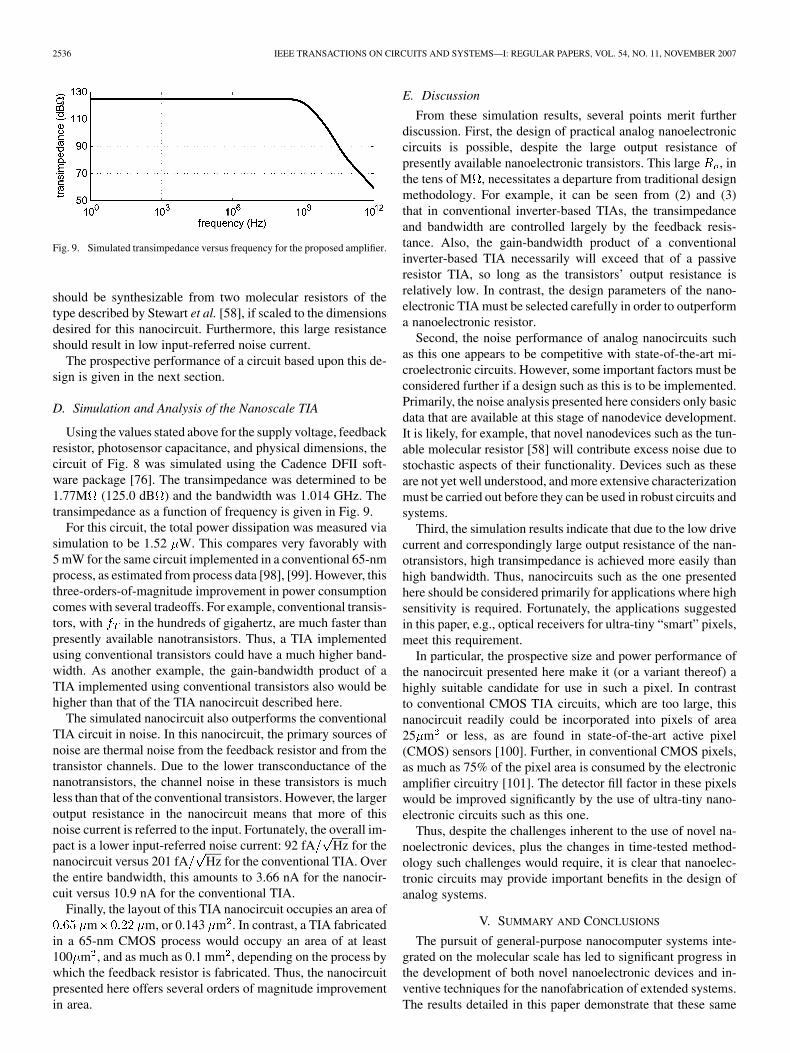
Fig. 9. Simulated transimpedance versus frequency for the proposed amplifier.
should be synthesizable from two molecular resistors of thetype described by Stewart et al. [58], if scaled to the dimensionsdesired for this nanocircuit. Furthermore, this large resistanceshould result in low input-referred noise current.
The prospective performance of a circuit based upon this de-sign is given in the next section.
D. Simulation and Analysis of the Nanoscale TIA
Using the values stated above for the supply voltage, feedbackresistor, photosensor capacitance, and physical dimensions, thecircuit of Fig. 8 was simulated using the Cadence DFII soft-ware package [76]. The transimpedance was determined to be1.77M (125.0 dB ) and the bandwidth was 1.014 GHz. Thetransimpedance as a function of frequency is given in Fig. 9.
For this circuit, the total power dissipation was measured viasimulation to be 1.52 W. This compares very favorably with5 mW for the same circuit implemented in a conventional 65-nmprocess, as estimated from process data [98], [99]. However, thisthree-orders-of-magnitude improvement in power consumptioncomes with several tradeoffs. For example, conventional transis-tors, with in the hundreds of gigahertz, are much faster thanpresently available nanotransistors. Thus, a TIA implementedusing conventional transistors could have a much higher band-width. As another example, the gain-bandwidth product of aTIA implemented using conventional transistors also would behigher than that of the TIA nanocircuit described here.
The simulated nanocircuit also outperforms the conventionalTIA circuit in noise. In this nanocircuit, the primary sources ofnoise are thermal noise from the feedback resistor and from thetransistor channels. Due to the lower transconductance of thenanotransistors, the channel noise in these transistors is muchless than that of the conventional transistors. However, the largeroutput resistance in the nanocircuit means that more of thisnoise current is referred to the input. Fortunately, the overall im-pact is a lower input-referred noise current: 92 fA Hz for thenanocircuit versus 201 fA Hz for the conventional TIA. Overthe entire bandwidth, this amounts to 3.66 nA for the nanocir-cuit versus 10.9 nA for the conventional TIA.
Finally, the layout of this TIA nanocircuit occupies an area ofm m, or 0.143 m . In contrast, a TIA fabricated
in a 65-nm CMOS process would occupy an area of at least100 m , and as much as 0.1 mm , depending on the process bywhich the feedback resistor is fabricated. Thus, the nanocircuitpresented here offers several orders of magnitude improvementin area.
E. Discussion
From these simulation results, several points merit furtherdiscussion. First, the design of practical analog nanoelectroniccircuits is possible, despite the large output resistance ofpresently available nanoelectronic transistors. This large , inthe tens of M , necessitates a departure from traditional designmethodology. For example, it can be seen from (2) and (3)that in conventional inverter-based TIAs, the transimpedanceand bandwidth are controlled largely by the feedback resis-tance. Also, the gain-bandwidth product of a conventionalinverter-based TIA necessarily will exceed that of a passiveresistor TIA, so long as the transistors’ output resistance isrelatively low. In contrast, the design parameters of the nano-electronic TIA must be selected carefully in order to outperforma nanoelectronic resistor.
Second, the noise performance of analog nanocircuits suchas this one appears to be competitive with state-of-the-art mi-croelectronic circuits. However, some important factors must beconsidered further if a design such as this is to be implemented.Primarily, the noise analysis presented here considers only basicdata that are available at this stage of nanodevice development.It is likely, for example, that novel nanodevices such as the tun-able molecular resistor [58] will contribute excess noise due tostochastic aspects of their functionality. Devices such as theseare not yet well understood, and more extensive characterizationmust be carried out before they can be used in robust circuits andsystems.
Third, the simulation results indicate that due to the low drivecurrent and correspondingly large output resistance of the nan-otransistors, high transimpedance is achieved more easily thanhigh bandwidth. Thus, nanocircuits such as the one presentedhere should be considered primarily for applications where highsensitivity is required. Fortunately, the applications suggestedin this paper, e.g., optical receivers for ultra-tiny “smart” pixels,meet this requirement.
In particular, the prospective size and power performance ofthe nanocircuit presented here make it (or a variant thereof) ahighly suitable candidate for use in such a pixel. In contrastto conventional CMOS TIA circuits, which are too large, thisnanocircuit readily could be incorporated into pixels of area25 m or less, as are found in state-of-the-art active pixel(CMOS) sensors [100]. Further, in conventional CMOS pixels,as much as 75% of the pixel area is consumed by the electronicamplifier circuitry [101]. The detector fill factor in these pixelswould be improved significantly by the use of ultra-tiny nano-electronic circuits such as this one.
Thus, despite the challenges inherent to the use of novel na-noelectronic devices, plus the changes in time-tested method-ology such challenges would require, it is clear that nanoelec-tronic circuits may provide important benefits in the design ofanalog systems.
V. SUMMARY AND CONCLUSIONS
The pursuit of general-purpose nanocomputer systems inte-grated on the molecular scale has led to significant progress inthe development of both novel nanoelectronic devices and in-ventive techniques for the nanofabrication of extended systems.The results detailed in this paper demonstrate that these same
DAS et al.: DESIGNS FOR ULTRA-TINY, SPECIAL-PURPOSE NANOELECTRONIC CIRCUITS 2537
devices and techniques also might be applied to an applicationspace that is relatively unexplored for nanoelectronics, that ofsmaller, special-purpose nanoelectronic circuits. Furthermore,these results indicate that substantial benefits might be obtainedfor applications if such nanocircuits can be utilized.
To illustrate these points, two example nanocircuits have beenexamined above, one digital and one analog. The digital circuit,a control nanocircuit for an autonomous millirobot, would bean enabling technology for such a robot. The design and sim-ulations considered here demonstrate that with presently avail-able nanotechnologies, the necessary control circuitry could bemade to fit within the desired form factor for the robot. Thus, it islikely that a nanoelectronic circuit designed using the principlesdescribed here could be useful in addressing the broader issue offurther miniaturizing micromachine systems. Utilizing nanocir-cuitry such as that described here, it is hoped that such circuit-machine systems might integrate both the control circuit andthe MEMS mechanisms in one very small package. These verymuch smaller, “smart” mechanisms could have many potentialapplications wherever MEMS devices presently are being inves-tigated for use: from communication networks, to biomedicaltherapeutics, to the millirobot addressed in this research.
Likewise, the analog nanocircuit described in this paper, aTIA for an optoelectronic sensor or receiver, could enable highbandwidth optical communications in a very small form factor.Designs such as the one presented for this amplifier also couldenable “smart pixel” sensor arrays to be realized. The anal-ysis presented for this amplifier demonstrates that analog na-noelectronics can provide more complex functionality for sucha sensor system, while simultaneously increasing the area avail-able for optical detection.
Example nanocircuits such as these provide strong motivationfor further investigation and development of application-spe-cific, special-purpose nanoelectronic circuits and systems. Thedesigns and simulations presented in this paper bear out in de-tail the premise that via the use of nanoelectronics, substantialimprovements in size and power may be obtained over existingsystems. Further, new applications may be enabled by the de-velopment of such nanocircuits. Thus, significant opportunitiesexist in the near future for fabrication and prototyping experi-ments to realize these benefits for important applications.
ACKNOWLEDGMENT
The authors thank Prof. A. DeHon of the University ofPennsylvania, Prof. J. Heath of the California Institute ofTechnology, Prof. C. Lieber of Harvard University, plus R.S. Williams, P. Kuekes, D. Stewart, and G. Snider of theHewlett-Packard Corporation for their many generous discus-sions and for providing information regarding their nanoscaledevices and system designs.
REFERENCES
[1] A. Bachtold, P. Hadley, T. Nakanishi, and C. Dekker, “Logic cir-cuits with carbon nanotube transistors,” Sci, vol. 294, no. 5545, pp.1317–1320, Nov. 9, 2001.
[2] C. P. Husband, S. M. Husband, J. S. Daniels, and J. M. Tour, “Logic andmemory with nanocell circuits,” IEEE Trans. Electron Devices, vol. 50,no. 9, pp. 1865–1875, Sep. 2003.
[3] R. K. Kummamuru, J. Timler, G. Toth, C. S. Lent, R. Ramasubrama-niam, A. O. Orlov, G. H. Bernstein, and G. L. Snider, “Power gain in aquantum-dot cellular automata latch,” Appl. Phys. Lett., vol. 81, no. 7,pp. 1332–1334, Aug. 12, 2002.
[4] C. P. Collier, E. W. Wong, M. Belohradsky, F. M. Raymo, J. F. Stod-dart, P. J. Kuekes, R. S. Williams, and J. R. Heath, “Electronicallyconfigurable molecular-based logic gates,” Sci, vol. 285, no. 5426, pp.391–394, Jul. 1999.
[5] C. P. Collier, G. Mattersteig, E. W. Wong, Y. Luo, K. Beverly, J. Sam-paio, F. M. Raymo, J. F. Stoddart, and J. R. Heath, “A [2]catenane-based solid state electronically reconfigurable switch,” Sci, vol. 289,pp. 1172–1175, 2000.
[6] Y. Luo, C. P. Collier, J. O. Jeppesen, K. A. Nielson, E. Delonno, G.Ho, J. Perkins, H. Tseng, T. Yamamoto, J. F. Stoddart, and J. R. Heath,“Two-Dimensional molecular electronics circuits,” ChemPhysChem,vol. 3, no. 6, pp. 519–525, Jun. 17, 2002.
[7] Y. Chen, D. A. A. Ohlberg, X. Li, D. R. Stewart, J. O. Jeppesen, K. A.Nielsen, J. F. Stoddart, D. L. Olynick, and E. Anderson, “Nanoscalemolecular-switch devices fabricated by imprint lithography,” Appl.Phys. Lett., vol. 82, no. 10, pp. 1610–1612, Mar. 2003.
[8] Y. Chen, G. Y. Jung, D. A. A. Ohlberg, X. M. Li, D. R. Stewart,J. O. Jeppesen, K. A. Nielsen, J. F. Stoddart, and R. S. Williams,“Nanoscale molecular-switch crossbar circuits,” Nanotechnology, vol.14, pp. 462–468, 2003.
[9] Y. Huang, X. F. Duan, Y. Cui, L. J. Lauhon, K. H. Kim, and C.M. Lieber, “Logic gates and computation from assembled nanowirebuilding blocks,” Sci, vol. 294, no. 5545, pp. 1313–1317, 2001.
[10] A. B. Greytak, L. J. Lauhon, M. S. Gudiksen, and C. M. Lieber,“Growth and transport properties of complementary germaniumnanowire field-effect transistors,” Appl. Phys. Lett., vol. 84, no. 21, pp.4176–4178, May 2004.
[11] Y. Cui, Z. Zhong, D. Wang, W. U. Wang, and C. M. Lieber, “Highperformance silicon nanowire field effect transistors,” Nano Lett., vol.3, pp. 149–152, 2003.
[12] P. J. Kuekes, D. R. Stewart, and R. S. Williams, “The crossbar latch:Logic value storage, restoration, and inversion in crossbar circuits,” J.Appl. Phys., vol. 97, pp. 034 301-1–034 301-5, 2005.
[13] J. Chen, M. A. Reed, A. M. Rawlett, and J. M. Tour, “Large on–off ratioand negative differential resistance in a molecular electronic device,”Sci, vol. 286, pp. 1550–1552, 1999.
[14] S. J. Tans, A. Verschueren, and C. Dekker, “Room-temperature tran-sistor based on a single carbon nanotube,” Nature, vol. 393, no. 6680,pp. 49–52, May 1998.
[15] S. J. Wind, J. Appenzeller, R. Martel, V. Derycke, and P. Avouris, “Ver-tical scaling of carbon nanotube field-effect transistors using top gateelectrodes,” Appl. Phys. Lett., vol. 80, no. 20, pp. 3817–3819, May 20,2002.
[16] G. Stix, “Nanotubes in the clean room,” Sci. Amer., pp. 82–85, Feb.2005.
[17] A. Javey et al., “High performance n-type carbon nanotube field-effecttransistors with chemically doped contacts,” Nano Lett., vol. 5, no. 2,pp. 345–348, 2005.
[18] G. S. Snider and P. J. Kuekes, “Nano state machines using hystereticresistors and diode crossbars,” IEEE Trans. Nano., vol. 5, pp. 129–137,2006.
[19] W. Wang, T. Lee, and M. A. Reed, “Electrical characterization of self-assembled monolayers,” in CRC Handbook on Molecular and NanoElectronics, S. E. Lyshevski, Ed. Boca Raton, FL: CRC, 2007.
[20] R. Metzger, “Unimolecular electronics: Results and prospects,” in CRCHandbook on Molecular and Nano Electronics, S. E. Lyshevski, Ed.Boca Raton, FL: CRC, 2007.
[21] K. S. Kwok and J. C. Ellenbogen, “Moletronics: Future electronics,”Mater. Today, vol. 5, no. 2, pp. 28–37, Feb. 1, 2002.
[22] J. C. Ellenbogen and J. C. Love, “Architectures for molecularelectronic computers. I. logic structures and an adder designedfrom molecular electronic diodes,” Proc. IEEE, vol. 88, no. 3,pp. 386–426, Mar. 2000.
[23] J. R. Heath, “Wires, switches, and wiring. A route toward a chemicallyassembled electronic nanocomputer,” Pure Appl. Chem., vol. 72, no.1–2, pp. 11–20, 2000.
[24] P. Beckett and A. Jennings, “Towards nanocomputer architecture,” inProc. Asia-Pacific Comp. Syst. Arch. Conf., 2002, pp. 141–150.
[25] A. DeHon, “Array-based architecture for fet-based, nanoscale elec-tronics,” IEEE Trans. Nanotechnol., vol. 2, no. 1, pp. 23–32, Mar. 2003.
[26] A. DeHon, P. Lincoln, and J. E. Savage, “Stochastic assembly of sub-lithographic nanoscale interfaces,” IEEE Trans. Nanotechnol., vol. 2,no. 3, pp. 165–174, Sep. 2003.
2538 IEEE TRANSACTIONS ON CIRCUITS AND SYSTEMS—I: REGULAR PAPERS, VOL. 54, NO. 11, NOVEMBER 2007
[27] A. DeHon and M. J. Wilson, “Nanowire-based sublithographic pro-grammable logic arrays,” in Proc. ACM/SIGDA FPGA, Monterey, CA,2004, pp. 123–132.
[28] M. Forshaw, R. Stadler, D. Crawley, and K. Nikolic, “A short reviewof nanoelectronic architectures,” Nanotechnology, vol. 15, no. 4, pp.S220–S223, 2004.
[29] J. R. Heath, P. J. Kuekes, G. S. Snider, and R. S. Williams, “A defect-tolerant computer architecture: Opportunities for nanotechnology,” Sci,vol. 280, no. 5370, pp. 1716–1721, Jun. 12, 1998.
[30] S. C. Goldstein and M. Budiu, “Nanofabrics: Spatial computing usingmolecular electronics,” in Proc. Int. Symp. Comp. Arch., Jun. 2001, pp.178–191.
[31] G. Snider, P. Kuekes, and R. S. Williams, “CMOS-like logic indefective, nanoscale crossbars,” Nanotechnology, vol. 15, no. 8, pp.881–891, Aug. 1, 2004.
[32] G. S. Rose and M. R. Stan, “Memory arrays based on molecular RTDdevices,” in Proc. IEEE-NANO, 2003, pp. 453–456.
[33] M. R. Stan, G. S. Rose, and M. M. Ziegler, “Hybrid cmos/molecularelectronic circuits,” in Proc. 19th Int. Conf. VLSI Design Held Jointly5th Int. Conf. Embedded Syst. Design, Hyderabad, India, Jan. 2006, pp.703–708.
[34] Z. Zhong, D. Wang, Y. Cui, M. W. Bockrath, and C. M. Lieber,“Nanowire crossbar arrays as address decoders for integrated nanosys-tems,” Sci, vol. 302, no. 5649, pp. 1377–1379, Nov. 21, 2003.
[35] K. K. Likharev and D. B. Strukov, “CMOL: Devices, circuits, and ar-chitectures,” Lect. Notes Phys., vol. 680, pp. 447–478, 2005.
[36] D. B. Strukov and K. K. Likharev, “Defect-tolerant architectures fornanoelectronic crossbar memories,” J. Nanosci. Nanotech., vol. 7, no.1, pp. 151–167, Aug. 2006.
[37] D. B. Strukov and K. K. Likharev, “A reconfigurable architecture forhybrid cmos/nanodevice circuits,” in Proc. ACM/SIGDA FPGA, Mon-terey, CA, 2006.
[38] W. Wu, G. Y. Jung, D. L. Olynick, J. Straznicky, Z. Li, X. Li, D. A.A. Ohlberg, Y. Chen, S. Y. Wang, J. A. Liddle, W. M. Tong, and R. S.Williams, “One-kilobit cross-bar molecular memory circuits at 30-nmhalf-pitch fabricated by nanoimprint lithography,” Appl. Phys., vol. 80,pp. 1173–1178, 2005.
[39] P. J. Kuekes, G. S. Snider, and R. S. Williams, “Crossbar nanocom-puters,” Sci. Amer., pp. 72–80, Nov. 2005.
[40] D. K. Brock, J. W. Ward, C. Bertin, B. M. Segal, and T. Rueckes, “Fab-rication and applications of single-walled carbon nanotube fabrics,” inCRC Nanomanufacturing Handbook, A. Busnaina, Ed. Boca Raton,FL: CRC, 2006, pp. 41–64.
[41] J. E. Green, J. W. Choi, A. Boukai, Y. Bunimovich, E. John-ston-Halperin, E. DeIonno, Y. Luo, B. A. Sheriff, K. Xu, Y. S. Shin,H.-R. Tseng, J. F. Stoddart, and J. R. Heath, “A 160-kilobit molecularelectronic memory patterned at 10 bits per square centimetre,”Nature, vol. 445, pp. 414–417, 2007.
[42] G. S. Snider and R. S. Williams, “Nano/CMOS architectures using afield-programmable nanowire interconnect,” Nanotechnology, vol. 18,no. 035204, pp. 178–191, 2007.
[43] K. S. J. Pister, J. M. Kahn, and B. E. Boser, “Smart dust: Wirelessnetworks of millimeter-scale sensor nodes,” in Electron. Res. Lab. Res.Summary, 1999.
[44] R. A. Freitas, Jr., Nanomedicine. Austin, TX: Landes Bioscience,1999, vol. I.
[45] A. Cavalcanti and R. A. Freitas, Jr., “Nanorobotics control design: Acollective behavior approach for medicine,” IEEE Trans. Nanobiosci.,vol. 4, no. 2, pp. 133–140, Jun. 2005.
[46] T. Hogg, “Coordinating microscopic robots for nanomedicine,” pre-sented at the 1st Very Small Robots Workshop, McLean, VA, Feb.2005, unpublished.
[47] SDR Forum, SDR Forum, Denver, CO [Online]. Available:http://www.sdrforum.org
[48] M. Cummings and S. Haruyama, “FPGA in the software radio,” IEEECommun. Mag., pp. 108–112, Feb. 1999.
[49] RFID Journal, RFID Journal, Melville, NY [Online]. Available: http://www.rfidjournal.com
[50] D. Routenberg and J. C. Ellenbogen, Design for a millimeter-scalewalking robot The MITRE Corporation, McLean, VA, report MP0W00000010, 2000.
[51] G. Snider, P. Kuekes, T. Hogg, and R. S. Williams, “Nanoelectronicarchitectures,” Appl. Phys., vol. 80, no. 6, pp. 1183–1195, Mar. 2005.
[52] S. R. Forrest and H. S. Hinton, Eds., IEEE J. Quantum Elect., Spec.Iss. Smart Pixels, vol. 29, no. 2, 1993.
[53] R. M. Metzger, “All about ( n-hexadecylquinolin-4-ium-1-yl) methyli-denetricyanoquinodimethanide, a unimolecular rectifier of electricalcurrent,” J. Mater. Chem., vol. 10, pp. 55–62, 2000.
[54] M. M. Ziegler, C. A. Picconatto, J. C. Ellenbogen, A. DeHon, D.Wang, Z. H. Zhong, and C. M. Lieber, “Scalability simulations fornanomemory systems integrated on the molecular scale,” in MolecularElectronics III. New York: Ann. N.Y. Acad. Sci., 2003, vol. 1006,pp. 312–330.
[55] R. M. Metzger, “Six unimolecular rectifiers and what lies ahead,” Lect.Notes Phys., vol. 680, pp. 313–350, 2005.
[56] K. K. Likharev, “SET: Coulomb blockade devices,” Nano Et MicroTechnol., vol. 3, pp. 71–114, 2003.
[57] Y. Cui and C. M. Lieber, “Functional nanoscale electronics devicesassembled using silicon nanowire building blocks,” Sci, vol. 291, pp.851–853, 2001.
[58] D. R. Stewart, D. A. A. Ohlberg, P. A. Beck, Y. Chen, R. S. Williams, J.O. Jeppesen, K. A. Nielsen, and J. F. Stoddart, “Molecule-independentelectrical switching in pt/organic monolayer/ti devices,” Nano Lett.,vol. 4, no. 1, pp. 133–136, 2004.
[59] S. Das, G. S. Rose, M. M. Ziegler, C. A. Picconatto, and J. C. El-lenbogen, “Architectures and simulations for nanoprocessor systemsintegrated on the molecular scale,” Lect. Notes Phys., vol. 680, pp.479–512, 2005.
[60] N. A. Melosh, A. Boukai, F. Diana, B. Gerardot, A. Badolato, P. M.Petroff, and J. R. Heath, “Ultrahigh-Density nanowire lattices and cir-cuits,” Sci, vol. 300, no. 5616, pp. 112–115, Apr. 4, 2003.
[61] G. Y. Jung, S. Ganapathiappan, X. Li, D. A. A. Ohlberg, D. L. Olynick,Y. Chen, W. M. Tong, and R. S. Williams, “Fabrication of molecular-electronic circuits by nanoimprint lithography at low temperatures andpressures,” Appl. Phys. Mater. Sci. & Process., vol. 78, no. 8, pp.1169–1173, May 1, 2004.
[62] G. Y. Jung, S. Ganapathiappan, D. A. A. Ohlberg, D. L. Olynick, Y.Chen, W. M. Tong, and R. S. Williams, “Fabrication of a 34 � 34crossbar structure at 50-nm half-pitch by uv-based nanoimprint lithog-raphy,” Nano Lett., vol. 4, no. 7, pp. 1225–1229, 2004.
[63] M. D. Austin, H. Ge, W. Wu, M. Li, Z. Yu, D. Wasserman, S. A. Lyon,and S. Y. Chou, “Fabrication of 5 nm linewidth and 14 nm pitch fea-tures by nanoimprint lithography,” Appl. Phys. Lett., vol. 84, no. 26,pp. 5299–5301, Jun. 2004.
[64] D. Whang, S. Jin, Y. Wu, and C. M. Lieber, “Large-scale hierarchicalorganization of nanowire arrays for integrated nanosystems,” NanoLett., vol. 3, no. 9, pp. 1255–1259, Sep. 2003.
[65] S. Hollar, A. Flynn, C. Bellew, and K. S. J. Pister, “Solar powered 10mg silicon robot,” in Proc. 16th Annu. Intl. IEEE Conf. MEMS, 2003,pp. 706–711.
[66] R. Yeh, S. Hollar, and K. S. J. Pister, “Design of low-power siliconarticulated microrobots,” J. Micromechatronics, vol. 1, no. 3, pp.191–203, 2001.
[67] M. Taczak, J. Ludwig, A. Gates, and J. C. Ellenbogen, “Mil-limeter-scale robotics at the MITRE corporation,” presented at the1st Very Small Robots Workshop, McLean, VA, Feb. 2005 [Online].Available: http://www.mitre.org/tech/nanotech/ourwork/pdf/Mil-limeter-scale_Robotics_at_MITRE.pdf, unpublished
[68] R. D. Beer, R. D. Quinn, H. J. Chiel, and R. E. Ritzmann, “Biologicallyinspired approaches to robotics: What can we learn from insects?,”Commun. ACM, vol. 40, no. 3, pp. 30–38, Mar. 1, 1997.
[69] B. Lee and I. Lee, “The implementation of the gaits and body structurefor hexapod robot,” in Proc. 2001 IEEE Intl. Symp. Indus. Elect., 2001,vol. 3, pp. 1959–1964.
[70] D. B. Strukov and K. K. Likharev, “CMOL FPGA: A reconfigurablearchitecture for hybrid digital circuits with two-terminal nanodevices,”Nanotechnology, vol. 16, pp. 888–900, 2005.
[71] D. B. Strukov, “Digital architectures for hybrid cmos/nanodevice cir-cuits,” Ph.D. thesis, Stony Brook University, Stony Brook, NY, 2006.
[72] D. Hammerstrom, “Defect tolerant CMOL cell assignment via satisfia-bility,” in Symp. Nanoelectronic Devices For Defense Security, CrystalCity, VA, Jun. 2007.
[73] X. M. H. Huang, C. A. Zorman, M. Mehregany, and M. L. Roukes,“Quality factor issues in silicon carbide nanomechnical resonators,” in12th Intl. Conf. Sol. St. Sens., Act. Microsys., 2003, pp. 722–725.
[74] S. Das and M. F. Bauwens, “Clocking nanocircuits for nanocomputersand other nanoelectronic systems ,” in Proc. IEEE/ACM Int. Symp.Nanoscale Architectures, to be published.
[75] M. R. Stan, P. D. Franzon, S. C. Goldstein, J. C. Lach, and M. M.Ziegler, “Molecular electronics: From devices and interconnect to cir-cuits and architecture,” Proc. IEEE, vol. 91, no. 11, pp. 1940–1957,Nov. 2003.
[76] Cadence Design Framework II, Version IC 5.0.33, Cadence DesignSystems, Inc., San Jose, CA, 2004.
[77] TSMC Standard Cell Library Datasheet, Cadence Design Systems,Inc., San Jose, CA, Nov. 2006 [Online]. Available: http://www.ca-dence.com
DAS et al.: DESIGNS FOR ULTRA-TINY, SPECIAL-PURPOSE NANOELECTRONIC CIRCUITS 2539
[78] Chip watch: Microprocessor Report, In-Stat, Waltham, MA, Sep. 2006[Online]. Available: http://www.mdronline.com/mpr/chip_watch/index.html
[79] The Integrated Nanosystems Site, MITRE, McLean, VA, Sep. 2006[Online]. Available: http://www.mitre.org/tech/nanotech/
[80] LM741 Datasheet, Rev. 5.0, Fairchild Semiconductor , South Portland,ME, 2000 [Online]. Available: http://www.fairchildsemi.com
[81] Intel Microprocessor Quick Reference Guide, Intel , Hillsboro, OR,Dec. 2006 [Online]. Available: http://www.intel.com/pressroom/kits/quickreffam.htm
[82] D. A. Johns and K. Martin, Analog Integrated Circuit Design. NewYork: Wiley, 1997.
[83] L. Pan, M. Zhang, and Y. Nakayama, “Growth mechanism of carbonnanocoils,” J. Appl. Phys., vol. 91, no. 12, 2002.
[84] P. C. P. Watts and W. K. Hsu, “Verification of electromagnetic induc-tion from fe-filled carbon nanotubes,” Appl. Phys., vol. 78, pp. 79–83,2004.
[85] D. C. Oertel, M. G. Bawendi, A. C. Arango, and V. Bulovic, “Photode-tectors based on treated cdse quantum-dot films,” Appl. Phys. Lett., vol.87, pp. 213 505-1–213 505-3, 2005.
[86] M. S. Gudiksen, L. J. Lauhon, J. Wang, D. C. Smith, and C. M. Lieber,“Growth of nanowire superlattice structures for nanoscale photonicsand electronics,” Nature, vol. 415, pp. 617–620, 2002.
[87] H. Kind, H. Yan, B. Messer, M. Law, and P. Yang, “Nanowire ultravi-olet photodetectors and optical switches,” Adv. Mat., vol. 14, no. 2, pp.158–160, 2002.
[88] F. Qian, Y. Li, S. Gradecak, D. Wang, C. J. Barrelet, and C. M. Lieber,“Gallium nitride-based nanowire radial heterostructures for nanopho-tonics,” Nano Lett., vol. 4, no. 10, pp. 1975–1979, 2004.
[89] T. Kuykendall, P. J. Pauzauskie, Y. Zhang, J. Goldberger, D. Sirbuly,J. Denlinger, and P. Yang, “Crystallographic alignment of high-densitygalium nitride nanowire arrays,” Nature Mater., vol. 3, pp. 524–528,2004.
[90] R. Agarwal and C. M. Lieber, “Semiconductor nanowires: Optics andoptoelectronics,” Appl. Phys., vol. 85, no. 3, pp. 209–215, 2006.
[91] J. Timler and C. S. Lent, “Power gain and dissipation in quantum-dotcellular automata,” J. Appl. Phys., vol. 91, no. 2, pp. 823–831, Jan. 15,2002.
[92] C. S. Lent, B. Isaksen, and M. Lieberman, “Molecular quantum-dot cel-lular automata,” J. Amer. Chem. Soc., vol. 125, no. 4, pp. 1056–1063,2003.
[93] Y. Huang, X. Duan, Q. Wei, and C. M. Lieber, “Directed assemblyof one-dimensional nanostructures into functional networks,” Sci, vol.291, pp. 630–633, Jan. 2001.
[94] R. T. Howe and C. G. Sodini, Microelectronics: An Integrated Ap-proach. Upper Saddle River, NJ: Prentice-Hal, 1997.
[95] M. A. Reed, “Quantum dots,” Sci. Amer., pp. 118–123, Jan. 1993.[96] R. A. Pease, “What’s all this transimpedance amplifier stuff, anyhow?,”
Electron. Design, Jan. 8, 2001.[97] I. O’Connor and F. Gaffiot, “Advanced research in on-chip optical in-
terconnects,” in Low-Power Electronics Design, C. Piguet, Ed. BocaRaton, FL: CRC , 2005.
[98] P. Bai et al., “A 65-nm logic technology featuring 35-nm gate lengths,enhanced channel strain, 8 cu interconnect layers, low-k ILD and0.57-�m SRAM cell,” in Proc. IEDM, Dec. 2004, pp. 657–660.
[99] W.-H. Lee et al., “High-performance 65-nm SOI technology with en-hanced transistor strain and advanced-low-k BEOL,” in Proc. IEDM,Dec. 2005.
[100] R. Turchetta, “Monolithic active pixel sensors: Design for science atCCLRC,” in PPARC Ind. Active Pixel Sensors Ind. Workshop, London,U.K., Mar. 2004.
[101] S. Mullen, “CMOS technology primer,” Digital Content Pro-ducer Oct. 2006 [Online]. Available: http://www.digitalcontentpro-ducer.com/hdhdv/depth/cmos_tech_hdv_10092006/
Shamik Das (M’03) received the S.B. degreein mathematics, the S.B. and M.Eng. degrees inelectrical engineering, and the Ph.D. degree inelectrical engineering and computer science fromthe Massachusetts Institute of Technology (MIT),Cambridge, in 2000 and 2004, respectively.
He joined The MITRE Corporation, McLean, VA,in 2004. He leads the effort to design, simulate, andanalyze nanoelectronic systems in the NanosystemsGroup at MITRE. In that role, he has made impor-tant contributions to the development of prototypes
for extended nanomemory systems, as well as to the design and analysis of cir-cuits for nanoprocessors. He has written and lectured broadly on the topic ofnanoelectronic system design and simulation. In addition, he has been engagedin a number of other projects at MITRE, such as the design of novel techniquesfor hyperspectral imaging, analysis of bio-inspired electronics, and multi-scalemodeling of physical systems. His technical interests include electronics aboveand beyond silicon, future computing systems, and systems engineering on thenanometer scale, as well as theoretical physics, acoustics, and pure mathematics.
In addition to the IEEE, Dr. Das is a member of Sigma Xi and Phi Beta Kappa.
Alexander J. Gates is presently working towardB.A. degrees in physics and mathematics at CornellUniversity, Ithaca, NY.
His research interests include nanoelectronic sys-tems and materials. Since June 2004, Mr. Gates alsohas been employed as a Research Investigator in theNanosystems Group, The MITRE Corporation, McL-lean, VA, where he has worked on projects in nano-electronic design and quantum molecular simulation.
Hassen A. Abdu (S’06) received the S.B. degree inelectrical engineering from the Massachusetts Insti-tute of Technology (MIT), Cambridge, in 2006. Hecurrently is pursuing the M.Eng. degree in electricalengineering at MIT, where he is working on organicand quantum dot memory devices.
Since June 2004, Mr. Abdu also has been em-ployed as a research investigator in the NanosystemsGroup, The MITRE Corporation, McLean, VA,where he has worked on projects in nanoelectronicdesign and simulation.
Mr. Abdu is a member of Eta Kappa Nu and Sigma Xi.
Garrett S. Rose (S’98–M’06) received the B.S.degree in computer engineering from VirginiaPolytechnic Institute and State University (VirginiaTech), Blacksburg, in 2001 and the M.S. and Ph.D.degrees in electrical engineering from the Universityof Virginia, Charlottesville, in 2003 and 2006,respectively.
He is currently an Assistant Professor in the De-partment of Electrical and Computer Engineering atPolytechnic University, Brooklyn, NY. Since 2004,he also has worked part time with The MITRE Cor-
poration, McLean, VA, where he is involved in the simulation of nanoscalesystems. His current research interests include VLSI circuit design and devel-oping VLSI design methodologies for nanoelectronics, with a specific interestin molecular electronics.
Carl A. Picconatto received the B.S. degree inchemistry from the University of Notre Dame, NotreDame, IN, and the Ph.D. degree in chemistry fromColumbia University, New York, in 1993 and 2000,respectively.
He is the Lead Scientist in the NanosystemsGroup, The MITRE Corporation, McLean, VA, andPrincipal Investigator of MITRE’s Nano-EnabledEnergy Storage Research Project. In addition, heserves as the nanotechnology laboratory directorfor the MITRE Biotechnology-Nanotechnology
Experimental Laboratory. His present research efforts include the use ofnanotechnology for energy and power systems, materials research with carbonnanotubes, and theoretical investigations into the electrical characteristics ofmolecules. Previously, he led MITRE’s effort to develop methods for the designand simulation of novel nanoelectronic memories and processors, which con-tributed greatly to the realization of the first prototype nanoelectronic systems.
2540 IEEE TRANSACTIONS ON CIRCUITS AND SYSTEMS—I: REGULAR PAPERS, VOL. 54, NO. 11, NOVEMBER 2007
Prior to joining MITRE, he served in the United States Congress as the ChiefScience Advisor to Congresswoman Constance A. Morella, a senior memberof the House Committee on Science. He also has worked for the Committee onScience, Engineering, and Public Policy at the National Academy of Sciences.
Dr. Picconatto is a member of the American Association for the Advance-ment of Science, American Chemical Society, and Phi Beta Kappa.
James C. Ellenbogen (M’03) received the B.A. de-gree in chemistry from the State University of NewYork, Buffalo, the M.S. degree in chemical physicsfrom the University of Wisconsin, Madison, and thePh.D. degree in chemical physics from the Universityof Georgia, Athens, in 1970, 1972 and 1977, respec-tively.
He is Senior Principal Scientist in the Nanosys-tems Group, The MITRE Corporation, McLean, VA,and Principal Investigator of MITRE’s NanosystemsModeling and Nanoelectronic Computers Research
Project. During the past 15 years, he has devoted his energies to furtheringthe science and technology for designing and developing nanosystems, such aselectronic computers integrated on the nanometer scale. He has collaborated inthe development of unique designs for molecular-scale electronic devices andco-authored several widely cited technical articles on nanoelectronics and nan-otechnology. He has been instrumental in the realization of the first prototypenanoelectronic systems. His efforts in the design and simulation of nanoelec-tronic systems also have led to the discovery of new principles of physics thatgovern the electrical properties of molecular devices. He taught at several uni-versities before joining The MITRE Corporation in 1984.
Dr. Ellenbogen is the recipient of the 1984 Barchi Prize of the Military Op-erations Research Society, the DARPA Ultra Electronics Program OutstandingService Award in 1998, and the 2005 Washington Academy of Sciences Awardfor Work of Merit and Distinction in the Engineering Sciences.