Charge Collection Analysis and SEU Modeling of SiGe HBTs for … · 2004-01-23 · 1 Charge...
15
1 Charge Collection Analysis and SEU Modeling of SiGe HBTs for High-Speed Digital Logic 2002 Single Event Effects Symposium, Manhattan Beach, CA, April 2002 Guofu Niu, John D. Cressler , Ramkumar Krithivasan, Pamela Riggs 1 , Barbara Randall 1 , Paul Marshall 2 , Robert Reed 3 , and Barry Gilbert 1 Alabama Microelectronics Science and Technology Center Electrical and Computer Engineering Department 200 Broun Hall, Auburn University, Auburn, AL 36849, USA 1 Mayo Foundation, Rochester, MN 55905 USA 2 Consultant to NASA-GSFC 3 NASA-GSFC, Code 562, Greenbelt, MD 20771, USA This work was supported by DTRA, NASA-GSFC, and the Auburn University CSPAE.
Transcript of Charge Collection Analysis and SEU Modeling of SiGe HBTs for … · 2004-01-23 · 1 Charge...

1
Charge Collection Analysis and SEU Modeling of SiGe HBTs
for High-Speed Digital Logic
2002 Single Event Effects Symposium, Manhattan Beach, CA, April 2002
Guofu Niu, John D. Cressler, Ramkumar Krithivasan, Pamela Riggs 1, Barbara Randall 1, Paul Marshall 2, Robert Reed 3, and Barry Gilbert 1
Alabama Microelectronics Science and Technology CenterElectrical and Computer Engineering Department
200 Broun Hall, Auburn University, Auburn, AL 36849, USA
1 Mayo Foundation, Rochester, MN 55905 USA 2 Consultant to NASA-GSFC3 NASA-GSFC, Code 562, Greenbelt, MD 20771, USA
This work was supported by DTRA, NASA-GSFC, and the Auburn University CSPAE.

2
• Motivation• SiGe HBT Technology• Total Dose and SEU Data• Quasi-3D Charge Collection Analysis• Circuit-level Modeling of SEU• Preliminary Full-3D Simulations• Summary
Outline

3
• The Holy Grail of the Space Community:- IC technology space-qualified without additional hardening
• SiGe HBT BiCMOS Technology:- bandgap engineering in Si (high yield + low cost)- III-V device performance (> 70 GHz fmax)- system-on-a-chip integration (SiGe HBT + Si CMOS)
• Radiation Tolerance:- robust to total dose and displacement (gamma, neutron, proton) - But … sensitive to SEU
Question:
Can We Use TCAD to Understand the SEU Charge Collection and Aid in Circuit-level SEU Mitigation?
Motivation

4
• IBM’s First-Generation SiGe HBT BiCMOS Technology (5HP) - UHV/CVD epitaxial SiGe base- deep and shallow trench isolation- 5 layers of metal
• No intentional radiation hardening
SiGe HBT Parameters Device Cross-section
SiGe HBT Technology
Drawn Emitter Width (?m) 0.50Actual Emitter Width (?m) 0.42peak ? 115VA (V) 60peak fT (GHz) 50peak fmax (GHz) 70BVCEO (V) 3.3
5
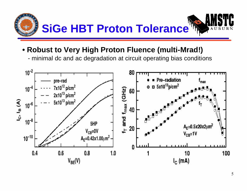
• Robust to Very High Proton Fluence (multi-Mrad!)- minimal dc and ac degradation at circuit operating bias conditions
SiGe HBT Proton Tolerance

6
• Low LET Threshold• Conventional III-V Hardening (CSH) Doesn’t Work!
Preliminary SEU Data
P. Marshall et al., IEEE Transactions on Nuclear Science, vol. 47, pp. 2669-2674, 2000.
7
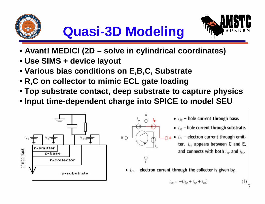
• Avant! MEDICI (2D – solve in cylindrical coordinates)• Use SIMS + device layout• Various bias conditions on E,B,C, Substrate• R,C on collector to mimic ECL gate loading • Top substrate contact, deep substrate to capture physics• Input time-dependent charge into SPICE to model SEU
Quasi-3D Modeling

8
• R and C load conditions matter!• Decrease in charge collection gives worse SEU!
Loading Effects
9
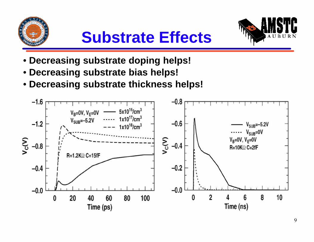
• Decreasing substrate doping helps!• Decreasing substrate bias helps!• Decreasing substrate thickness helps!
Substrate Effects

10
• Use ECL D-Flip flop as high-speed logic metric• Compare various architectures for same charge profile
Circuit-level SEU
Circuit A:Standard ECL
Circuit B:UnhardenedCSH
Circuit C:HardenedCSH
11
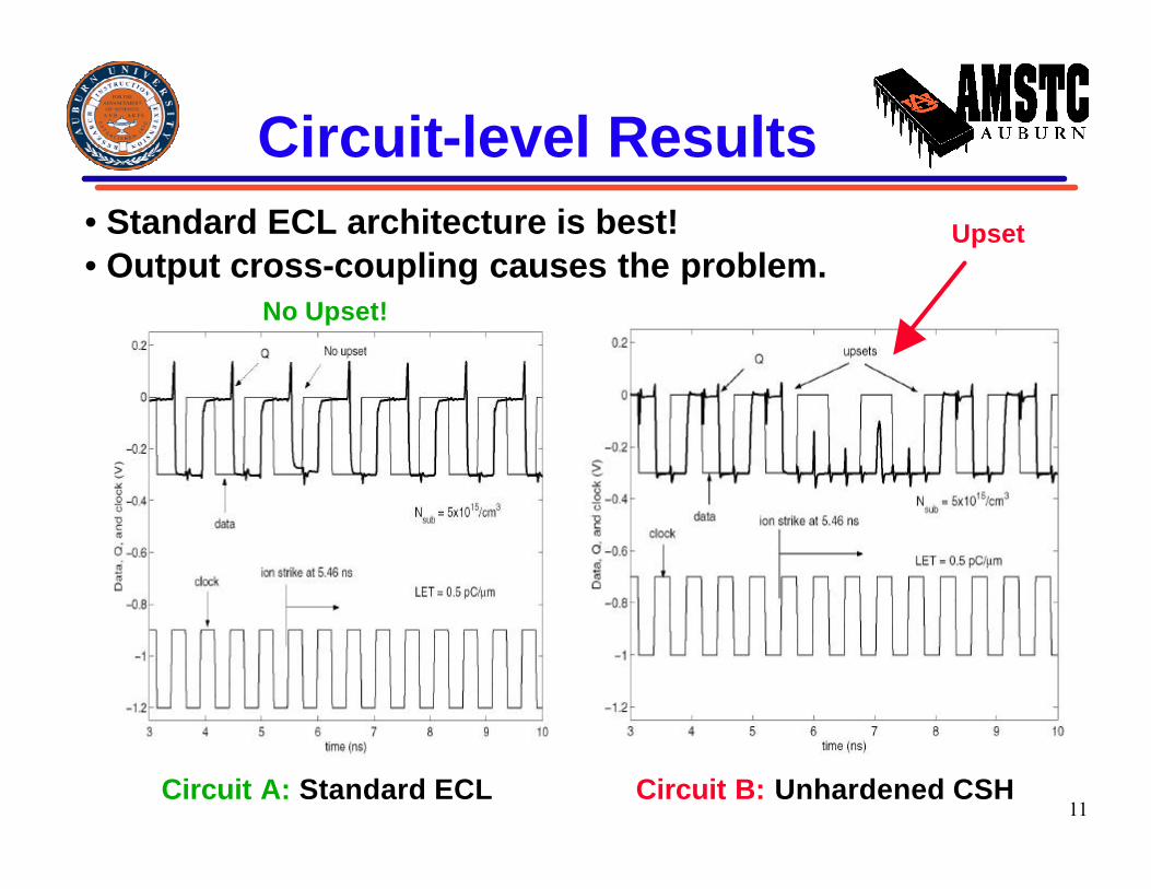
• Standard ECL architecture is best!• Output cross-coupling causes the problem.
Circuit-level Results
Circuit A: Standard ECL Circuit B: Unhardened CSH
Upset
No Upset!

12
• Full 3D Device Simulation- better physics- off-center strikes- tough problem!
• Tool: ISE (DESSIS)- SiGe capability- SEU capability
• Typical Run:- 15,572 nodes- 208 min per timestep!
Full 3D SEU Modeling
Substrate
Oxide
Emitter
Collector
Top Substrate
Base

13
• Ion Strike: LET = 10 (0.1 pC/um), 10 um depth, center of emitter• E=B=C=0V, Sx = -5V, RC = 1.2 k ohms, CC = 15 fF
Time Evolution
Initial Strike After 6.0 psec
B E C Sx B E C Sx

14
Time Evolution
After 50 psec After 200 psec
B E C SxB E C Sx

15
• SiGe HBT BiCMOS Technology- bandgap engineering in Si (high speed + low cost)- inherent dose tolerance, but SEU sensitivity exists
• TCAD Can Be Used To Understand SEU in SiGe HBTs- R,C loading and bias effects- substrate effects- circuit architecture matters! (standard design best – area penalty)- adequate SEU immunity appears possible for SiGe HBT logic
To Be Done:• Full 3D simulations• 3D versus quasi-3D comparison• True mixed-mode SEU simulation (not Q(t) + SPICE)• Microbeam experiment (data versus model)
Summary