BSI Technology with Bulk Si Wafer - Image Sensor S Workshops/2009 Workshop... · 1 Security C –...
53
1 Security C – TSMC Secret BSI Technology with Bulk Si Wafer S.G. Wuu RD; TSMC June 25 2009
Transcript of BSI Technology with Bulk Si Wafer - Image Sensor S Workshops/2009 Workshop... · 1 Security C –...

1
Security C –TSMC Secret
BSI Technology with Bulk Si Wafer
S.G. WuuRD; TSMC
June 25 2009
2
Security C –TSMC Secret
AcknowledgementS.G. Wuu1, C.C. Wang1, D.N. Yaung1, Y.L. Tu1, J.C. Liu1, T.H. Hsu1,
F.J. Shiu1, C.Y. Yu1, G.Y. Shiau1, R.J. Lin, C.S.Tsai1, L. Tran1,S.S. Chen1, C.C. Wang1, S.Y. Huang1,
H. Rhodes2, D. Tai2, Y. Qian2, D. Mao2, S. Manabe2, A. Shah2, R. Yang2,
J.C. Hsieh3, Calvin Chang3, C.W. Lu3, Shawn Tseng3,
Nick Wen4, C.Y. Ni4, C.A. Lin4
1Taiwan Semiconductor Manufacturing Company, Hsin-Chu, Taiwan, R.O.C.2OmniVision Technologies, Inc., 4275 Burton Drive, Santa Clara, CA 95054
3VisEra Technologies Company, Hsin-Chu, Taiwan, R.O.C.4Xintec, Inc., Chung-Li, Taiwan, R.O.C.

3
Security C –TSMC SecretOutline
OverviewSi Technology Color filter & Microlens Manufacturability Device Performance BSI Package Summary & Future TrendReference
4
Security C –TSMC Secret
BSI Overview
5
Security C –TSMC Secret
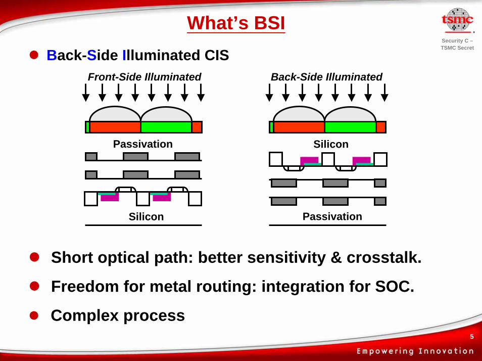
What’s BSIBack-Side Illuminated CIS
Short optical path: better sensitivity & crosstalk.
Freedom for metal routing: integration for SOC.
Complex process
Back-Side Illuminated
Silicon
Passivation
Front-Side Illuminated
Silicon
Passivation

6
Security C –TSMC Secret
CMOS Sensor Application & Technology
ToysToys
Surveillance Surveillance
Cellular Phone Cellular Phone
Res
olut
ion
PC CamPC CamAutomobileAutomobile
SurveillanceSurveillance(High End)(High End)
Digital CamDigital Cam(High End DSLR)(High End DSLR)
DigitalDigitalCam Cam
CIF
16M+
12M
8M
5M
3M
2M
1M
VGA
N90 N65
FSI BSI0.5µm 0.35µm 0.25µm 0.18µm 0.13µm 0.11µm N45
¼” Camera Module 2MP 3MP 5MP 8MP 12MP
Pixel Size 2.2um 1.75um 1.4um 1.1um 0.9um
7
Security C –TSMC Secret
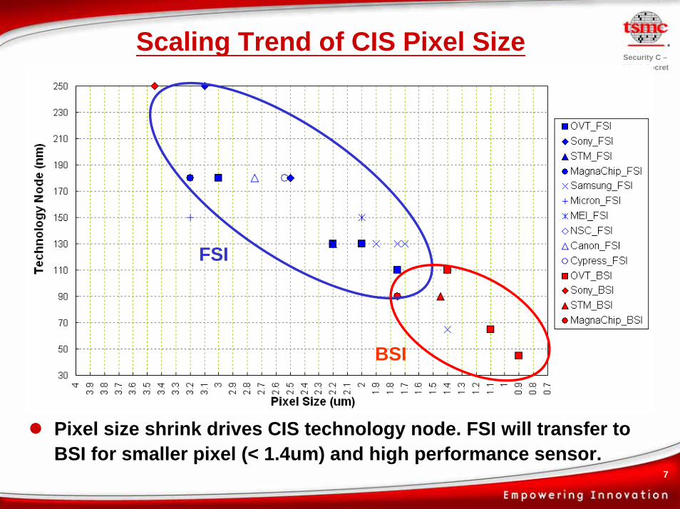
FSI
BSI
Scaling Trend of CIS Pixel Size
Pixel size shrink drives CIS technology node. FSI will transfer to BSI for smaller pixel (< 1.4um) and high performance sensor.

8
Security C –TSMC Secret
FSI/BSI Structure Comparison
Sensing area at 1.4um node: BSI gets double sensing area compare to FSI.Optical path: BSI get short optical path. FSI need to thin-down backend THK and saturate to 1.75um.
Sensing Area / Optical Path vs. Pixel Size
00.10.20.30.40.50.60.70.80.9
1
0.9 1.1 1.4 1.75 2.2 3
Pixel Size (um)
Nor
mal
ized
Sen
sing
Are
a
00.10.20.30.40.50.60.70.80.91
Nor
mal
ized
Opt
ical
Pat
h
FSI sensing area
BSI sensing area
FSI optical path
9
Security C –TSMC Secret
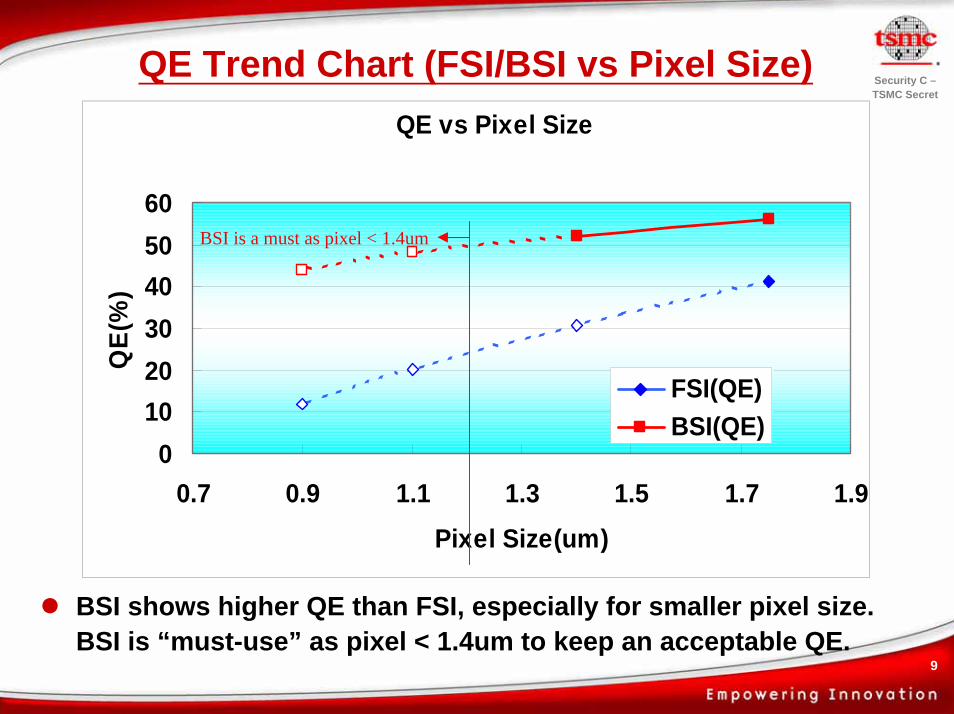
QE Trend Chart (FSI/BSI vs Pixel Size)QE vs Pixel Size
0102030405060
0.7 0.9 1.1 1.3 1.5 1.7 1.9Pixel Size(um)
QE(
%)
FSI(QE)BSI(QE)
BSI is a must as pixel < 1.4um
BSI shows higher QE than FSI, especially for smaller pixel size.BSI is “must-use” as pixel < 1.4um to keep an acceptable QE.
10
Security C –TSMC Secret
Si Technology in Module & Integration
11
Security C –TSMC Secret
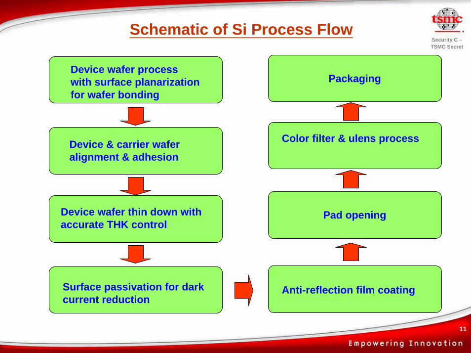
Schematic of Si Process Flow
PackagingDevice wafer process with surface planarization for wafer bonding
Device & carrier wafer alignment & adhesion
Color filter & ulens process
Pad openingDevice wafer thin down with accurate THK control
Anti-reflection film coatingSurface passivation for dark current reduction

12
Security C –TSMC Secret
BSI Bonding ProgressBubble free achievedBubble monitor methodology establishedGood planarization before bondParticle reduction @ bonding interfaceWafer bonder optimization
Bubble-freeBubble

13
Security C –TSMC Secret
Grinding PerformanceTTW (Total Thickness Variation) within Wafer: 2~3 um
No visible stripe pattern viewed by OM as demonstrated from small step height < 0.025um within 1.5mm scan range from Alpha-stepper
Wafer Center step height ~250A
Post Grinding THK Profile
4 1 . 0 0
4 2 . 0 0
4 3 . 0 0
4 4 . 0 0
4 5 . 0 0
4 6 . 0 0
4 7 . 0 0
-150 -100 -50 0 50 100 150Radius(mm)
THK
(um
)
Mean
+1
+2
+3
-1
-2
-3
Wafer Middle step height ~200A
Grinder artificial profile compensation for wet etch thin down process
Wafer Edge step height ~230A

14
Security C –TSMC Secret
BSI Thin Down Process
Non-SOI approach (TSMC IP chemicals for etch stop on Epi layer)
Mechanical & Wet chemical thin downWTW THK uniformity controlled @ ≤ +/- 0.025um by establishing feed-forward system
Good surface roughness with stripe pattern free
Stripe pattern from
optical image1 . 7
1 . 8
1 . 9
2
2 . 1
0 5 10 15 20 25Wafer number
THK
(um
)
Mean
+0.1
+0.2
-0.1
-0.2

15
Security C –TSMC Secret
Within Wafer Thickness UniformityTTV (Total Thickness Variation) within Wafer < +/- 0.1um Epi wafer requires special thin-down technique to maintain reasonable THK variation across waferSi THK variation causes optical response variation
1 . 6
1 . 7
1 . 8
1 . 9
2 . 0
2 . 1
2 . 2
1 3 5 7 9 11 13 15 17 19Position
THK
(um
)
OldOldNewNewNewNewSOISOI
Mean
+0.1
+0.2
+0.3
-0.1
-0.2
-0.3
16
Security C –TSMC Secret
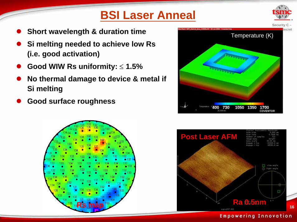
BSI Laser AnnealShort wavelength & duration time Si melting needed to achieve low Rs (i.e. good activation) Good WIW Rs uniformity: ≤ 1.5%No thermal damage to device & metal if Si meltingGood surface roughness
Temperature (K)
730400 1050 1350 1700
Rs map
Post Laser AFM
Ra 0.5nm
17
Security C –TSMC Secret
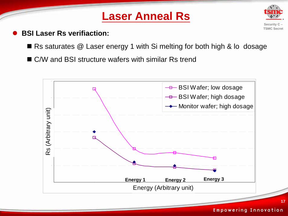
Laser Anneal RsBSI Laser Rs verifiaction:
Rs saturates @ Laser energy 1 with Si melting for both high & lo dosage
C/W and BSI structure wafers with similar Rs trend
0
2 0 0
4 0 0
6 0 0
8 0 0
1 0 0 0
1 2 0 0
1 . 2 1 . 4 1 . 6 1 . 8 2 2 . 2
Energy (Arbitrary unit)
Rs
(Arb
itrar
y un
it)
BSI Wafer; low dosageBSI Wafer; high dosageMonitor wafer; high dosage
Energy 1 Energy 2 Energy 3
18
Security C –TSMC Secret
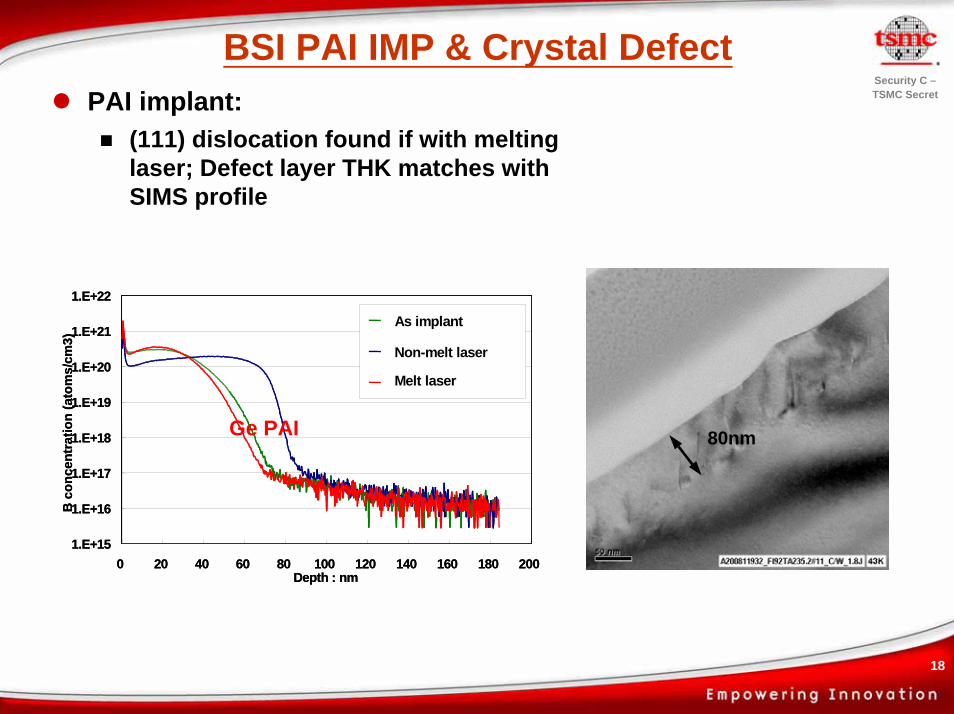
BSI PAI IMP & Crystal DefectPAI implant:
(111) dislocation found if with melting laser; Defect layer THK matches with SIMS profile
80nm
1.E+15
1.E+16
1.E+17
1.E+18
1.E+19
1.E+20
1.E+21
1.E+22
0 20 40 60 80 100 120 140 160 180 200Depth : nm
B c
once
ntra
tion
(ato
ms/
cm3)
2_1222_085230_FI9235_1.6J
2_1222_085230_FI9235_1.8J
2_1222_085230_FI9235_No_LA_W1
As implant
Non-melt laser
Melt laser
1.E+15
1.E+16
1.E+17
1.E+18
1.E+19
1.E+20
1.E+21
1.E+22
0 20 40 60 80 100 120 140 160 180 200Depth : nm
B c
once
ntra
tion
(ato
ms/
cm3)
2_1222_085230_FI9235_1.6J
2_1222_085230_FI9235_1.8J
2_1222_085230_FI9235_No_LA_W1
As implant
Non-melt laser
Melt laser
Ge PAI

19
Security C –TSMC Secret
Si TEM for BSI Process Improvement
(020)/(022) Crystal defectsInduced by thin down damage & Si melting/crystallizationSolved by extra thermal to remove thin down damage before laser anneal
TEM photos show original BSI process with specific defect density and defect free condition for improved process
[020]
[022] Plane-view
[020]
[022] Plane-view
Defect density ~0.567/um Defect free
20
Security C –TSMC Secret
BSI Si Technology A cost effective thin down approach by using bulk Si wafers with tight Si THK control by feed forward systemThe robust wafer edge integrity achieved by introducing an edge trimming toolA bonding recipe & setting with bubble free Successfully introduce laser anneal for backside implant activation and crystal defect eliminationImplementation of backside metal shield for black level referenceSmooth backside Si surface achieved to minimize its impact to image quality (e.g. stripe pattern, etc.)
1
Security C –TSMC Secret
Color Filter & Microlens Technology
2
Security C –TSMC Secret
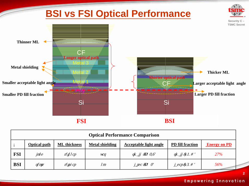
BSI vs FSI Optical Performance
Larger acceptable light angle
Larger PD fill fraction
Si Si
CF
CF
Metal 3
Metal 2
Metal 1
Poly
Thinner ML
Thicker ML
Smaller acceptable light angle
Metal shielding
Longer optical path
Shorter optical path
BSI
Smaller PD fill fraction
FSI
Optical Performance Comparison
Optical path ML thickness Metal shielding Acceptable light angle PD fill fraction Energy on PD
FSI long thinner yes small (F# 2.8) small (~30%) 27%
BSI short thicker no large (F# 2) lager (~50%) 56%

3
Security C –TSMC SecretVariant green color filter material can optimize sensitivity and
color X-talk.Green main peak shifts to 550 nmLower x-talk at green/blueHigher x-talk at green/red
Color Filter in BSI
Green_1Green_2RedBlueGreen_3
Lower x-talk
4
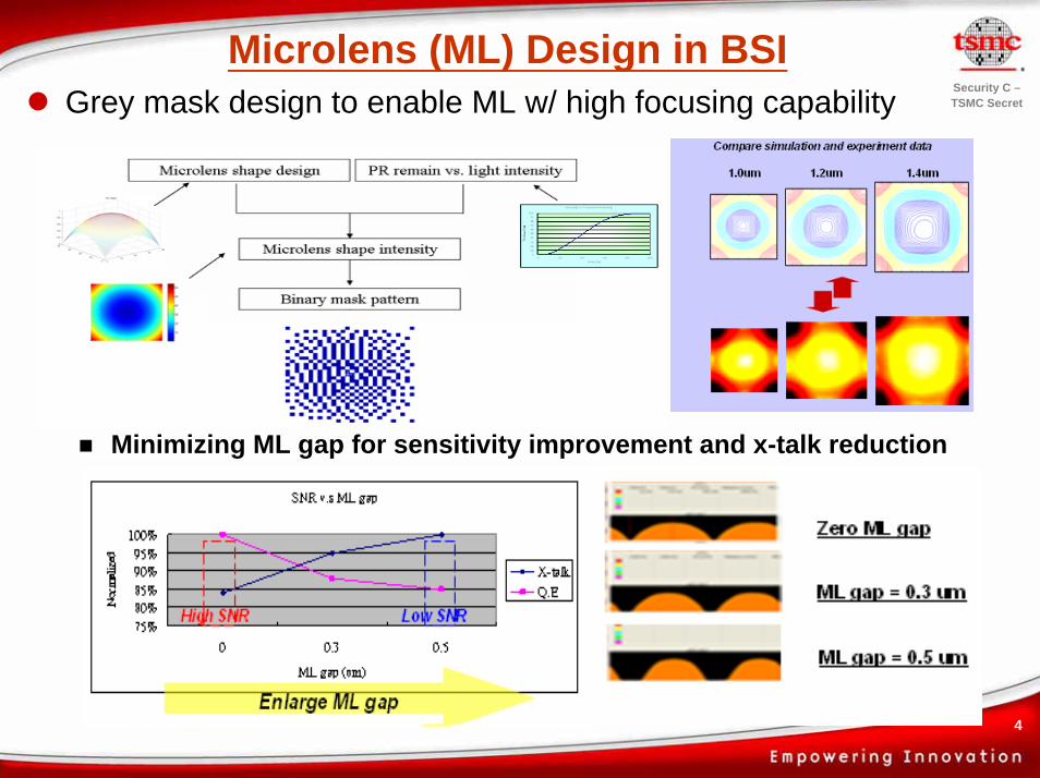
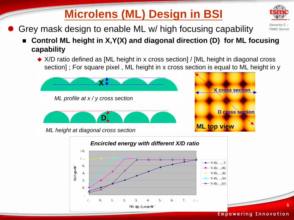
Security C –TSMC SecretGrey mask design to enable ML w/ high focusing capability
Minimizing ML gap for sensitivity improvement and x-talk reduction
Microlens (ML) Design in BSI
5
Security C –TSMC SecretGrey mask design to enable ML w/ high focusing capability
Control ML height in X,Y(X) and diagonal direction (D) for ML focusing capability
X/D ratio defined as [ML height in x cross section] / [ML height in diagonal cross section] ; For square pixel , ML height in x cross section is equal to ML height in y cross section
Microlens (ML) Design in BSI
ML profile at x / y cross section
ML height at diagonal cross section ML top view
X cross section
ML height = 0.6 um for pixel size =1.4 um
0
20
40
60
80
100
120
10 20 30 40 50 60 70 80 90 100
PD fill factor (%)
Intensity (%)
X/D=0.07
X/D=0.28
X/D=0.58
X/D=0.72
X/D=0.85
Encircled energy with different X/D ratio
D
X
D cross section

6
Security C –TSMC Secret
Compared to FSI, the shading effect in BSI can be improved 40% by integrating sensor and lens in 1.4um pixel
Shading Effect Improvement in BSI
Lens
Sensor Improved ~40%

7
Security C –TSMC Secret
Future Trend-Gradient CML Different ML height and shifting arrangement based on CRA
Combined ML shifting and gradient height ML for shading optimization
35
40
45
50
55
60
65
70
-30 -20 -10 0 10 20 30
CRA (degree)
CML (ML height = 0.75)) Gradient ML (ML height =0.75~0.45)
15% improved at edge pixel
Sensitivity of edge pixel with large CRA( Shading Profile Simulation)
8
Security C –TSMC Secret
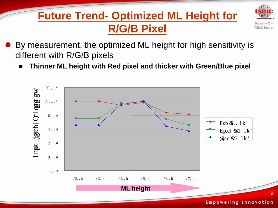
By measurement, the optimized ML height for high sensitivity is different with R/G/B pixels
Thinner ML height with Red pixel and thicker with Green/Blue pixel
Future Trend- Optimized ML Height for R/G/B Pixel
0.00%
20.00%
40.00%
60.00%
80.00%
100.00%
120.00%
1400j 1500j 1600j 1700j 1800j 1900j
dose energy
normalized_Sensitivity
Red (600 nm)
Green (530 nm)
Blue (450 nm)
ML height
9
Security C –TSMC Secret
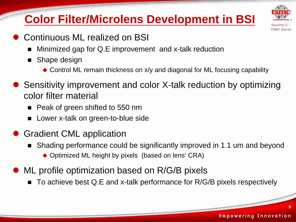
Continuous ML realized on BSI Minimized gap for Q.E improvement and x-talk reduction Shape design
Control ML remain thickness on x/y and diagonal for ML focusing capability
Sensitivity improvement and color X-talk reduction by optimizing color filter material
Peak of green shifted to 550 nmLower x-talk on green-to-blue side
Gradient CML applicationShading performance could be significantly improved in 1.1 um and beyond
Optimized ML height by pixels (based on lens’ CRA)
ML profile optimization based on R/G/B pixelsTo achieve best Q.E and x-talk performance for R/G/B pixels respectively
Color Filter/Microlens Development in BSI
10
Security C –TSMC Secret
BSI Manufacturability
11
Security C –TSMC Secret
Def
ectiv
e D
ie
0102030405060708090
100110120130140150160170180
Q1 08' Q2 08' Q3 08' Q4 08' Q1 09' Q2 09'Quarter
Type-F
Type-E
Type-D
Type-C
Type-B
Type-A
1.Tool kits lifetime control2.Chamber clean optimization3.Type-C defect from new process for opticalimprovement
1.PM procedure optimization2.Type-E defect from new process foroptical improvement
1.Process simplify2.Process relocation3.Tool H/W retrofit to fixdefect source
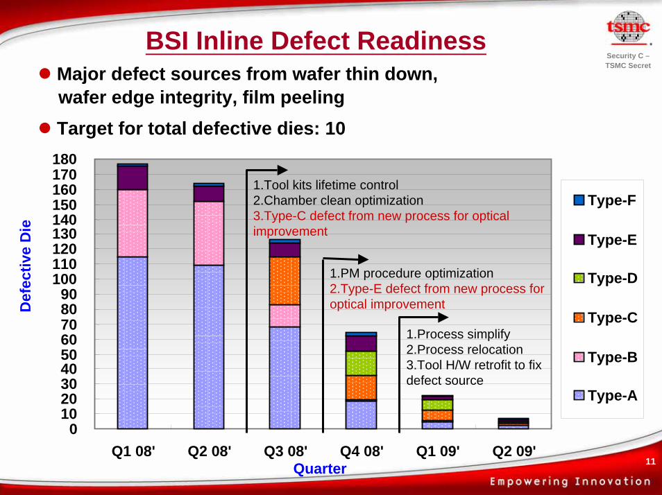
BSI Inline Defect ReadinessMajor defect sources from wafer thin down, wafer edge integrity, film peelingTarget for total defective dies: 10

12
Security C –TSMC Secret
Trimmer Particle ReductionTrimmer Particle Reduction
Background: Trimmer is used for wafer edge trimming before wafer bonding. The trimmer will induce many Si-dust particles in the trimming process. Trimmer Particle Reduction:Optimizing clean recipe with brusher to remove the trimmer particle.
Local map PA
EDX: Si, Al, O
13
Security C –TSMC Secret
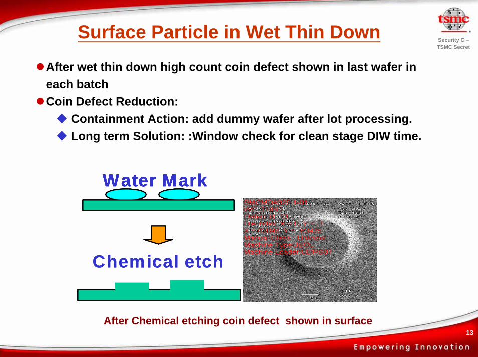
Surface Particle in Wet Thin Down
After wet thin down high count coin defect shown in last wafer in each batch Coin Defect Reduction:
Containment Action: add dummy wafer after lot processing.Long term Solution: :Window check for clean stage DIW time.
After Chemical etching coin defect shown in surface
Chemical etch
Water Mark
Chemical etch
Water MarkWater MarkWater Mark

14
Security C –TSMC Secret
BSI Cycle-time Improvement3.5A days cycle time reduction (4.2A 1.2A)
BSI Cycle Time Roadmap
4.2
3.6
2.8
2.01.7
1.4 1.2
0
1
2
3
4
5
Q1 08' Q2 08' Q3 08' Q4 08' Q1 09' Q2 09' Q3 09'
Cyc
le T
ime*
A d
ays
36% tool automation
100% tool automation
Process simplify Multi chamber tools released
Tool WPH improvement
Tool WPH improvement-2
15
Security C –TSMC Secret
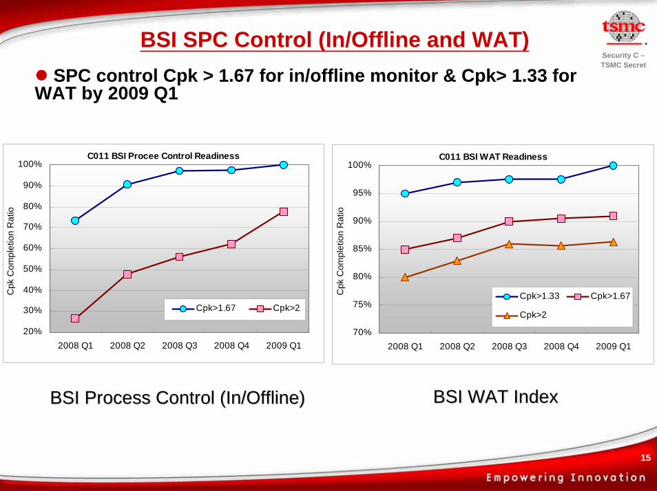
BSI SPC Control (In/Offline and WAT)SPC control Cpk > 1.67 for in/offline monitor & Cpk> 1.33 for
WAT by 2009 Q1
C011 BSI WAT Readiness
70%
75%
80%
85%
90%
95%
100%
2008 Q1 2008 Q2 2008 Q3 2008 Q4 2009 Q1C
pk C
ompl
etio
n R
atio
Cpk>1.33 Cpk>1.67
Cpk>2
C011 BSI Procee Control Readiness
20%
30%
40%
50%
60%
70%
80%
90%
100%
2008 Q1 2008 Q2 2008 Q3 2008 Q4 2009 Q1
Cpk
Com
plet
ion
Rat
io
Cpk>1.67 Cpk>2
BSI WAT IndexBSI WAT IndexBSI Process Control (In/Offline)BSI Process Control (In/Offline)

16
Security C –TSMC Secret
BSI Manufacturability Defect, particle, contamination are improved by optimizing chamber clean recipe and retrofitting tool hardwareIn line process monitor is performed by suitable Spec and metrology (FTIR, KLA, OP…. ) Cycle time is improved by high WPH(Wafer Per Hour) tool mixing run and automation run.Cost structure is improved by process/recipe simplification and low cost raw materialSPC control Cpk> 1.67 for in/off line monitor & Cpk> 1.33 for WAT are achieved for BSI manufacturing
17
Security C –TSMC Secret
Device and Characterization

18
Security C –TSMC Secret
Device PerformanceMOS Id-Vds behavior w/i & w/o optical illuminationDevice at low current bias condition behaves differently under illumination due to photo carrier generation
10um/0.13um Core NMOS
1.0E-14
1.0E-12
1.0E-10
1.0E-08
1.0E-06
1.0E-04
1.0E-02
-0.5 0 0.5 1 1.5 2
Vg(V)
ID(A
)
w/o optical illumination
w/ optical illumination
10um/0.13um Core PMOS
1.0E-14
1.0E-12
1.0E-10
1.0E-08
1.0E-06
1.0E-04
1.0E-02
-0.5 0 0.5 1 1.5 2
Vg(V)
ID(A
)w/o optical illumination
w/ optical illumination
19
Security C –TSMC Secret
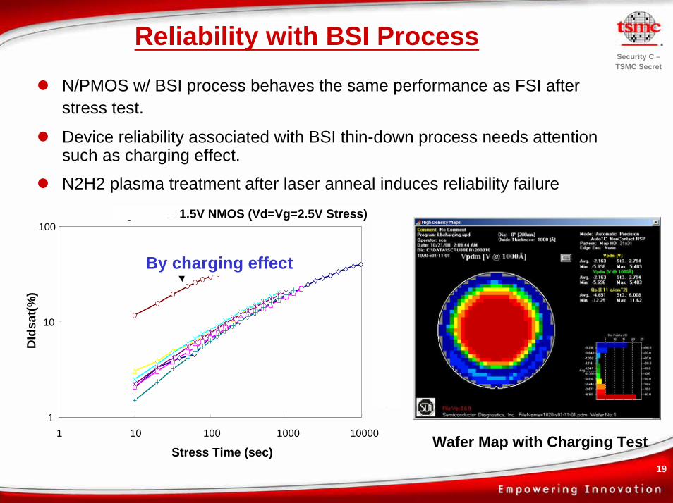
Reliability with BSI Process
N/PMOS w/ BSI process behaves the same performance as FSI after stress test.
Device reliability associated with BSI thin-down process needs attention such as charging effect.
N2H2 plasma treatment after laser anneal induces reliability failure
Q94684.3 1.5V NMOS (Vd=Vg=2.5V Stress)
1
10
100
1 10 100 1000 10000
Stress Time (sec)
DId
sat(%
)
By charging effect
Wafer Map with Charging Test
20
Security C –TSMC Secret
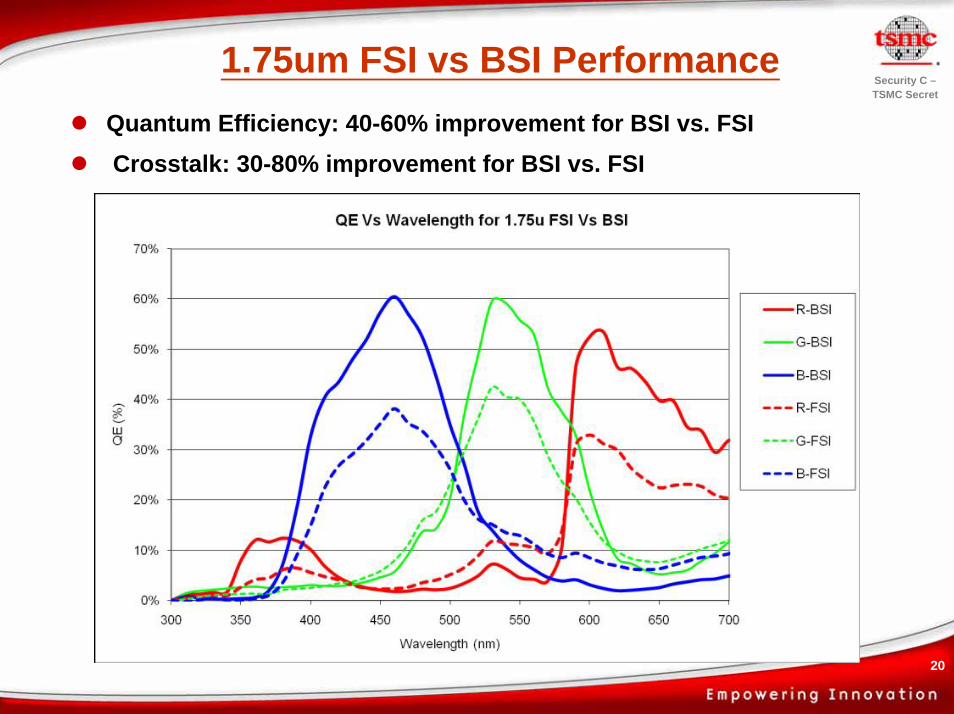
1.75um FSI vs BSI PerformanceQuantum Efficiency: 40-60% improvement for BSI vs. FSICrosstalk: 30-80% improvement for BSI vs. FSI

21
Security C –TSMC Secret
QE versus Si THKOn-target THK achieves optimized QE. Red and blue QE are more sensitive with THK control (~3% degradation with +-0.3um deviation)
Thinner Si degrades red response and thicker Si degrades QE in blue (due to carrier recombination)
40%
42%
44%
46%
48%
50%
52%
54%
56%
STD THK-0.3um STD THK STD THK+0.3um
Si THK
QE 600nm
530nm450nm

22
Security C –TSMC Secret
BSI Device Characterization Summary
MOS transistors at low bias current condition behave differently due to optical illumination.Charging effect by BSI tools detected and improved for reliabilityImplementation of backside P+ imp with laser anneal and backside ARC significantly improves QE 1.75um FSI vs BSI comparison: 20%-30% improvement in QE (R/G/B); xtalk 28%-67% reductionTight Si THK control is needed to avoid QE degradation (~3% QE deviation with +-0.3um Si control)

1
Security C –TSMC Secret
BSI Package Technology

2
Security C –TSMC Secret
3
Security C –TSMC Secret
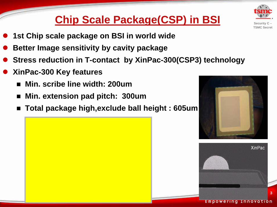
Chip Scale Package(CSP) in BSI 1st Chip scale package on BSI in world wide Better Image sensitivity by cavity package Stress reduction in T-contact by XinPac-300(CSP3) technology XinPac-300 Key features
Min. scribe line width: 200umMin. extension pad pitch: 300umTotal package high,exclude ball height : 605um
4
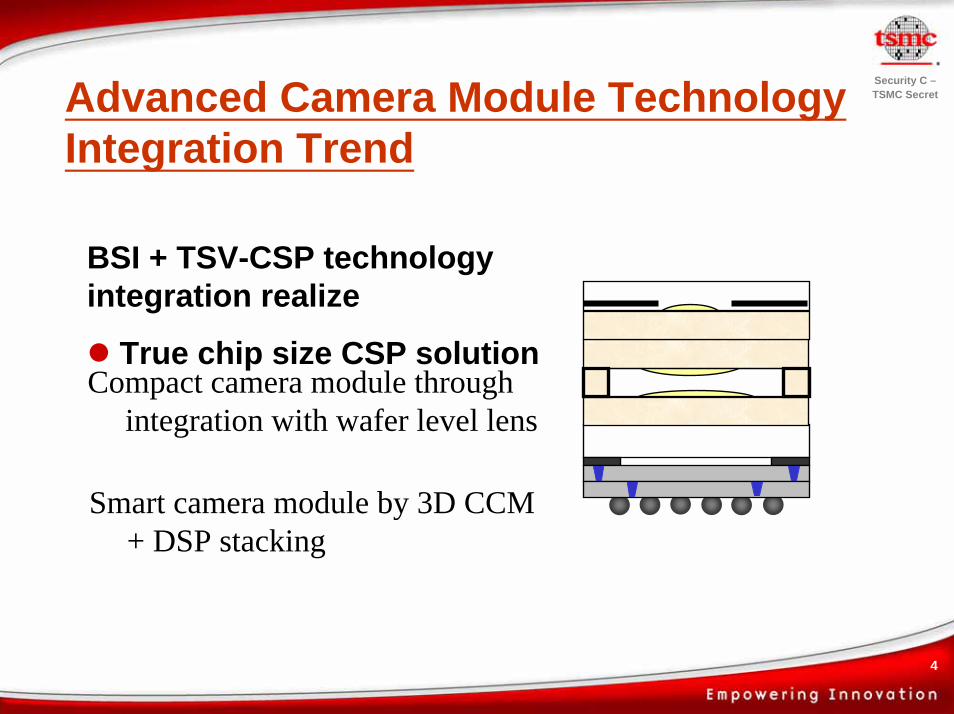
Security C –TSMC SecretAdvanced Camera Module Technology
Integration Trend
BSI + TSV-CSP technology integration realize
True chip size CSP solutionCompact camera module through
integration with wafer level lens
Smart camera module by 3D CCM + DSP stacking

5
Security C –TSMC SecretBSI + TSV CSP Benefits - More Gross Die
Circuit under pad design compatible and zero silicon real estate loss 5%~15% gross die gain compare with conventional sidewall CSP
0%
5%
10%
15%
20%
0 10 20 30 40 50Die size, in mm^2
BS
I+TS
V C
SP
v.s
. FS
I+TS
V C
SP
Gro
ss D
ie G
ain(
8" b
asis
)
Circuit under pad
6
Security C –TSMC Secret
BSI Package Technology Summary 0.11 BSI Achievements (BSI + CSP3) :
Achieve 1st Chip-Scale package on BSI in world wide Good Stress reduction in T- Contact & Competitive stack height by CSP3 technology
Next generation & future trend (BSI + TSV or 3D IC)
Smaller die size compare with COB/CSP3 solution
More gross dies through CUP compatible design
Enable low cost CCM (Compact Camera Module) via integration with wafer level lens module technology
Enhanced CSP reliability compared with conventional sidewall CSP technology
Enable pixel level interconnection through TSV technology

7
Security C –TSMC Secret
Summary & Future Trend
8
Security C –TSMC Secret
SummaryWorld’s first BSI image sensor w/ bulk Si in mass production – 1.75um & 1.4um pixelUtilization of epi wafers for BSI mass production with well Si THK controlAchieve more than 5x QE enhancement in BSI by backside P+ implant and ARC coatingAchieve dark current < 1 e/sec @ RT by surface optimization Achieve record low SNR=10 lux value -- 57 lux for 1.75um pixel and 105 lux for 1.4um pixelN65 BSI for 1.1 um pixel and beyond is under development and demonstrates the convincing manufacturing capability in 12” Cu Fab
9
Security C –TSMC Secret
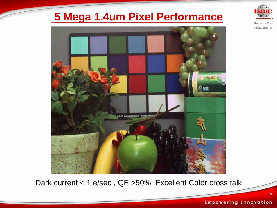
5 Mega 1.4um Pixel Performance
Dark current < 1 e/sec , QE >50%; Excellent Color cross talk

10
Security C –TSMC Secret
BSI Future Work
Tighter Epi-Si thickness control (< ±0.5um → < ±0.1um) on in-coming materials in order to further improve within wafer thickness uniformity (< ±0.1um)
Laser hardware improvement to tighten energy uniformity for Rs uniformity improvement (< 1.5%)
Yield enhancement through tight thickness control, uniform backside P+ activation, defect reduction & robust wafer edge engineering
Process cost down; WPH (Wafer Per Hour) improvement & Process simplification, etc.
CFA optimization to target 1.1um/0.9um pixel sizes and beyond in 300mm manufacturing.
TSV + CSP integration with BSI and wafer level camera module.
11
Security C –TSMC Secret
ReferenceTom Joy et al, “Development of a production-ready, back-illuminated CMOS image sensor with small pixels”, IEDM, p1007, 2007.Bedabrata Pain et al, “Wafer-level thinned CMOS imagers implemented in a bulk-CMOS technology”, IISW, 2007.Jens Primd et al, “A 3mega-pixel back-illuminated image sensor in 1T5 architecture with 1.45um pixel pitch”, IISW, 2007.Shin Iwabuchi et al, “A back-illuminated high-sensitivity small-pixel color CMOS image sensor with flexible layout of metal wiring”, ISSCC, p302, 2006.Jung Chak Ahn et al, “Advanced image sensor technology for pixel scaling down toward 1.0um (Invited)”, IEDM, p275, 2008.