dana holdings 0CA5D6ED-FF04-4642-9D47-81A0CF09F4AB_4Q08_ConfCall
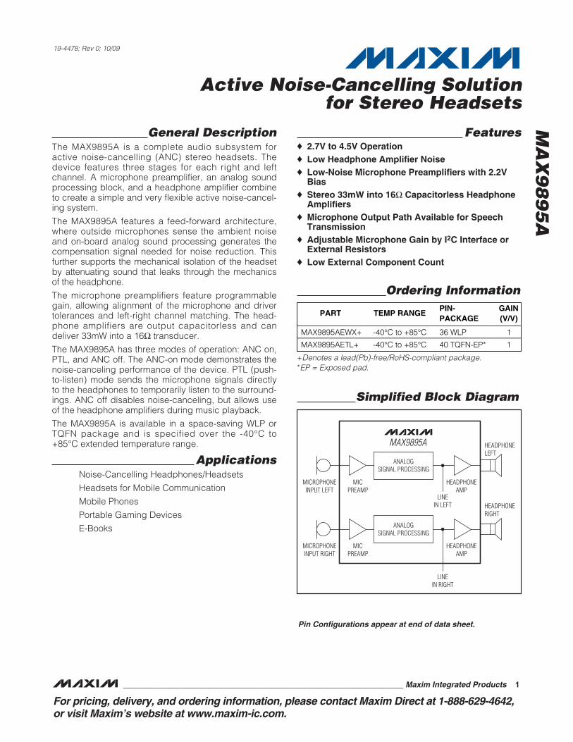
General DescriptionThe MAX9895A is a complete audio subsystem foractive noise-cancelling (ANC) stereo headsets. Thedevice features three stages for each right and leftchannel. A microphone preamplifier, an analog soundprocessing block, and a headphone amplifier combineto create a simple and very flexible active noise-cancel-ing system.
The MAX9895A features a feed-forward architecture,where outside microphones sense the ambient noiseand on-board analog sound processing generates thecompensation signal needed for noise reduction. Thisfurther supports the mechanical isolation of the headsetby attenuating sound that leaks through the mechanicsof the headphone.
The microphone preamplifiers feature programmablegain, allowing alignment of the microphone and drivertolerances and left-right channel matching. The head-phone amplifiers are output capacitorless and candeliver 33mW into a 16Ω transducer.
The MAX9895A has three modes of operation: ANC on,PTL, and ANC off. The ANC-on mode demonstrates thenoise-canceling performance of the device. PTL (push-to-listen) mode sends the microphone signals directlyto the headphones to temporarily listen to the surround-ings. ANC off disables noise-canceling, but allows useof the headphone amplifiers during music playback.
The MAX9895A is available in a space-saving WLP orTQFN package and is specified over the -40°C to+85°C extended temperature range.
ApplicationsNoise-Cancelling Headphones/Headsets
Headsets for Mobile Communication
Mobile Phones
Portable Gaming Devices
E-Books
Features 2.7V to 4.5V Operation Low Headphone Amplifier Noise Low-Noise Microphone Preamplifiers with 2.2V
Bias Stereo 33mW into 16Ω Capacitorless Headphone
Amplifiers Microphone Output Path Available for Speech
Transmission Adjustable Microphone Gain by I2C Interface or
External Resistors Low External Component Count
MA
X9
89
5A
Active Noise-Cancelling Solutionfor Stereo Headsets
________________________________________________________________ Maxim Integrated Products 1
19-4478; Rev 0; 10/09
For pricing, delivery, and ordering information, please contact Maxim Direct at 1-888-629-4642,or visit Maxim’s website at www.maxim-ic.com.
Pin Configurations appear at end of data sheet.
Ordering Information
PART TEMP RANGEPIN-PACKAGE
GAIN(V/V)
MAX9895AEWX+ -40°C to +85°C 36 WLP 1
MAX9895AETL+ -40°C to +85°C 40 TQFN-EP* 1
+Denotes a lead(Pb)-free/RoHS-compliant package.*EP = Exposed pad.
ANALOGSIGNAL PROCESSING
LINEIN LEFT
MICPREAMP
HEADPHONEAMP
HEADPHONELEFT
MICROPHONEINPUT LEFT
MAX9895A
ANALOGSIGNAL PROCESSING
LINEIN RIGHT
MICPREAMP
HEADPHONEAMP
HEADPHONERIGHT
MICROPHONEINPUT RIGHT
Simplified Block Diagram
MA
X9
89
5A
Active Noise-Cancelling Solutionfor Stereo Headsets
2 _______________________________________________________________________________________
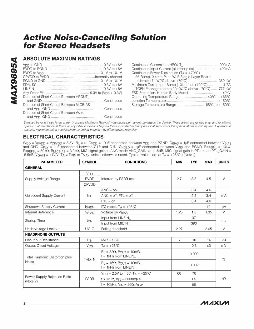
ABSOLUTE MAXIMUM RATINGS
Stresses beyond those listed under “Absolute Maximum Ratings” may cause permanent damage to the device. These are stress ratings only, and functionaloperation of the device at these or any other conditions beyond those indicated in the operational sections of the specifications is not implied. Exposure toabsolute maximum rating conditions for extended periods may affect device reliability.
VDD to GND..............................................................-0.3V to +6VPVDD to PGND.........................................................-0.3V to +6VPVDD to VDD .........................................................-0.1V to +0.1VCPVDD to PVDD...............................................Internally shortedPGND to GND .......................................................-0.1V to +0.1VSDA, SCL..................................................................-0.3V to +6VLINEIN_ ....................................................................-0.3V to +6VAny Other Pin .............................................-0.3V to (VDD + 0.3V)Duration of Short Circuit Between HPOUT_
and GND ................................................................ContinuousDuration of Short Circuit Between MICBIAS
and VDD, GND .......................................................ContinuousDuration of Short Circuit Between VMID
and VDD, GND .......................................................Continuous
Continuous Current into HPOUT_ .....................................200mAContinuous Input Current (all other pins) .........................±20mAContinuous Power Dissipation (TA = +70°C)
36-Bump, 0.4mm-Pitch WLP Single-Layer Board(derate 17mW/°C above +70°C)..............................1360mW
Maximum Current per Bump (10k hrs at +120°C) ................1.7ATQFN Package (derate 22mW/°C above +70°C) ......1777mW
ESD Protection, Human Body Model ...................................±2kVOperating Temperature Range ...........................-40°C to +85°CJunction Temperature ......................................................+150°CStorage Temperature Range .............................-65°C to +150°C
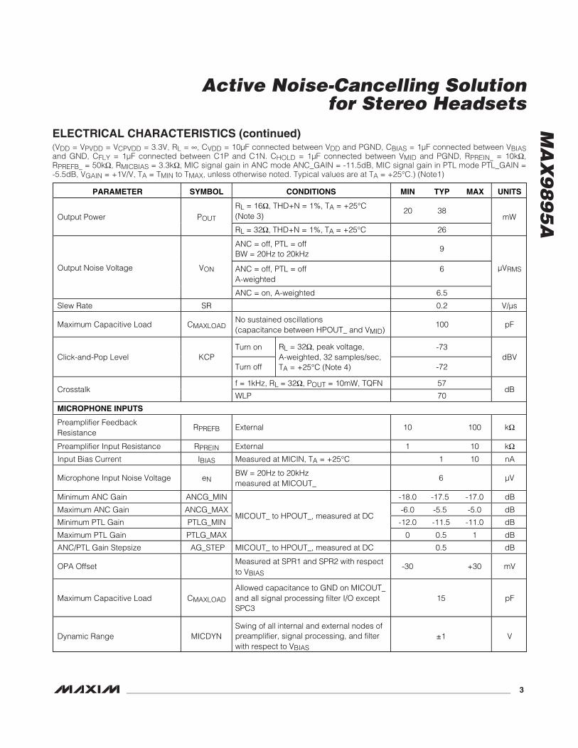
PARAMETER SYMBOL CONDITIONS MIN TYP MAX UNITS
GENERAL
VDD
PVDDSupply Voltage Range
CPVDD
Inferred by PSRR test 2.7 3.3 4.5 V
ANC = on 3.4 4.6
ANC = off, PTL = off 2.5 3.4Quiescent Supply Current IDD
PTL = on 3.4 4.6
mA
Shutdown Supply Current ISHDN I2C mode, TA = +25°C 12 µA
Internal Reference VBIAS Voltage on VBIAS 1.25 1.3 1.35 V
Input from LINEIN_ 37Startup Time tON
Input from MICIN_ 390ms
Undervoltage Lockout UVLO Falling threshold 2.27 2.65 V
HEADPHONE OUTPUTS
Line Input Resistance RIN MAX9895A 7 10 14 kΩOutput Offset Voltage VOS TA = +25°C 0.3 ±3 mV
RL = 32Ω, POUT = 10mW,f = 1kHz from LINEIN_
0.002Total Harmonic Distortion plusNoise
THD+NRL = 16Ω, POUT = 10mW,f = 1kHz from LINEIN_
0.002
%
VDD = 2.5V to 4.5V, TA = +25°C 60 70
f ≤ 1kHz, VIN = 200mVP-P 65Power-Supply Rejection Ratio(Note 2)
PSRR
f = 10kHz, VIN = 200mVP-P 55
dB
ELECTRICAL CHARACTERISTICS(VDD = VPVDD = VCPVDD = 3.3V, RL = ∞, CVDD = 10µF connected between VDD and PGND, CBIAS = 1µF connected between VBIASand GND, CFLY = 1µF connected between C1P and C1N. CHOLD = 1µF connected between VMID and PGND, RPREIN_ = 10kΩ,RPREFB_ = 50kΩ, RMICBIAS = 3.3kΩ, MIC signal gain in ANC mode ANC_GAIN = -11.5dB, MIC signal gain in PTL mode PTL_GAIN =-5.5dB, VGAIN = +1V/V, TA = TMIN to TMAX, unless otherwise noted. Typical values are at TA = +25°C.) (Note1)
MA
X9
89
5A
Active Noise-Cancelling Solutionfor Stereo Headsets
_______________________________________________________________________________________ 3
PARAMETER SYMBOL CONDITIONS MIN TYP MAX UNITS
RL = 16Ω, THD+N = 1%, TA = +25°C(Note 3)
20 38Output Power POUT
RL = 32Ω, THD+N = 1%, TA = +25°C 26
mW
ANC = off, PTL = offBW = 20Hz to 20kHz
9
ANC = off, PTL = offA-weighted
6
Output Noise Voltage VON
ANC = on, A-weighted 6.5
µVRMS
Slew Rate SR 0.2 V/µs
Maximum Capacitive Load CMAXLOADNo sustained oscillations(capacitance between HPOUT_ and VMID)
100 pF
Turn on -73Click-and-Pop Level KCP
Turn off
RL = 32Ω, peak voltage,A-weighted, 32 samples/sec,TA = +25°C (Note 4) -72
dBV
f = 1kHz, RL = 32Ω, POUT = 10mW, TQFN 57Crosstalk
WLP 70dB
MICROPHONE INPUTS
Preamplifier FeedbackResistance
RPREFB External 10 100 kΩ
Preamplifier Input Resistance RPREIN External 1 10 kΩInput Bias Current IBIAS Measured at MICIN, TA = +25°C 1 10 nA
Microphone Input Noise Voltage eNBW = 20Hz to 20kHzmeasured at MICOUT_
6 µV
Minimum ANC Gain ANCG_MIN -18.0 -17.5 -17.0 dB
Maximum ANC Gain ANCG_MAX -6.0 -5.5 -5.0 dB
Minimum PTL Gain PTLG_MIN -12.0 -11.5 -11.0 dB
Maximum PTL Gain PTLG_MAX
MICOUT_ to HPOUT_, measured at DC
0 0.5 1 dB
ANC/PTL Gain Stepsize AG_STEP MICOUT_ to HPOUT_, measured at DC 0.5 dB
OPA OffsetMeasured at SPR1 and SPR2 with respectto VBIAS
-30 +30 mV
Maximum Capacitive Load CMAXLOAD
Allowed capacitance to GND on MICOUT_and all signal processing filter I/O exceptSPC3
15 pF
Dynamic Range MICDYNSwing of all internal and external nodes ofpreamplifier, signal processing, and filterwith respect to VBIAS
±1 V
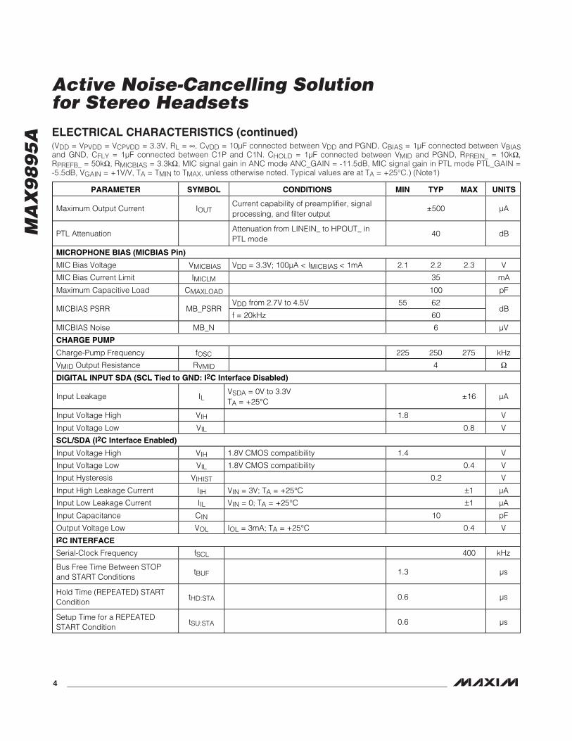
ELECTRICAL CHARACTERISTICS (continued)(VDD = VPVDD = VCPVDD = 3.3V, RL = ∞, CVDD = 10µF connected between VDD and PGND, CBIAS = 1µF connected between VBIASand GND, CFLY = 1µF connected between C1P and C1N. CHOLD = 1µF connected between VMID and PGND, RPREIN_ = 10kΩ,RPREFB_ = 50kΩ, RMICBIAS = 3.3kΩ, MIC signal gain in ANC mode ANC_GAIN = -11.5dB, MIC signal gain in PTL mode PTL_GAIN =-5.5dB, VGAIN = +1V/V, TA = TMIN to TMAX, unless otherwise noted. Typical values are at TA = +25°C.) (Note1)
MA
X9
89
5A
Active Noise-Cancelling Solutionfor Stereo Headsets
4 _______________________________________________________________________________________
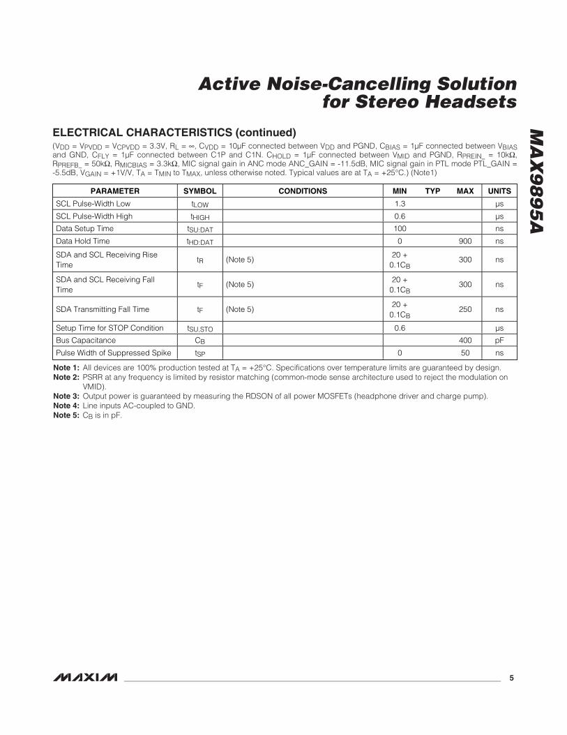
ELECTRICAL CHARACTERISTICS (continued)(VDD = VPVDD = VCPVDD = 3.3V, RL = ∞, CVDD = 10µF connected between VDD and PGND, CBIAS = 1µF connected between VBIASand GND, CFLY = 1µF connected between C1P and C1N. CHOLD = 1µF connected between VMID and PGND, RPREIN_ = 10kΩ,RPREFB_ = 50kΩ, RMICBIAS = 3.3kΩ, MIC signal gain in ANC mode ANC_GAIN = -11.5dB, MIC signal gain in PTL mode PTL_GAIN =-5.5dB, VGAIN = +1V/V, TA = TMIN to TMAX, unless otherwise noted. Typical values are at TA = +25°C.) (Note1)
PARAMETER SYMBOL CONDITIONS MIN TYP MAX UNITS
Maximum Output Current IOUTCurrent capability of preamplifier, signalprocessing, and filter output
±500 µA
PTL AttenuationAttenuation from LINEIN_ to HPOUT_ inPTL mode
40 dB
MICROPHONE BIAS (MICBIAS Pin)
MIC Bias Voltage VMICBIAS VDD = 3.3V; 100µA < IMICBIAS < 1mA 2.1 2.2 2.3 V
MIC Bias Current Limit IMICLM 35 mA
Maximum Capacitive Load CMAXLOAD 100 pF
VDD from 2.7V to 4.5V 55 62MICBIAS PSRR MB_PSRR
f = 20kHz 60dB
MICBIAS Noise MB_N 6 µV
CHARGE PUMP
Charge-Pump Frequency fOSC 225 250 275 kHz
VMID Output Resistance RVMID 4 ΩDIGITAL INPUT SDA (SCL Tied to GND: I2C Interface Disabled)
Input Leakage ILVSDA = 0V to 3.3VTA = +25°C
±16 µA
Input Voltage High VIH 1.8 V
Input Voltage Low VIL 0.8 V
SCL/SDA (I2C Interface Enabled)
Input Voltage High VIH 1.8V CMOS compatibility 1.4 V
Input Voltage Low VIL 1.8V CMOS compatibility 0.4 V
Input Hysteresis VIHIST 0.2 V
Input High Leakage Current IIH VIN = 3V; TA = +25°C ±1 µA
Input Low Leakage Current IIL VIN = 0; TA = +25°C ±1 µA
Input Capacitance CIN 10 pF
Output Voltage Low VOL IOL = 3mA; TA = +25°C 0.4 V
I2C INTERFACE
Serial-Clock Frequency fSCL 400 kHz
Bus Free Time Between STOPand START Conditions
tBUF 1.3 µs
Hold Time (REPEATED) STARTCondition
tHD:STA 0.6 µs
Setup Time for a REPEATEDSTART Condition
tSU:STA 0.6 µs
MA
X9
89
5A
Active Noise-Cancelling Solutionfor Stereo Headsets
_______________________________________________________________________________________ 5
ELECTRICAL CHARACTERISTICS (continued)(VDD = VPVDD = VCPVDD = 3.3V, RL = ∞, CVDD = 10µF connected between VDD and PGND, CBIAS = 1µF connected between VBIASand GND, CFLY = 1µF connected between C1P and C1N. CHOLD = 1µF connected between VMID and PGND, RPREIN_ = 10kΩ,RPREFB_ = 50kΩ, RMICBIAS = 3.3kΩ, MIC signal gain in ANC mode ANC_GAIN = -11.5dB, MIC signal gain in PTL mode PTL_GAIN =-5.5dB, VGAIN = +1V/V, TA = TMIN to TMAX, unless otherwise noted. Typical values are at TA = +25°C.) (Note1)
PARAMETER SYMBOL CONDITIONS MIN TYP MAX UNITS
SCL Pulse-Width Low tLOW 1.3 µs
SCL Pulse-Width High tHIGH 0.6 µs
Data Setup Time tSU:DAT 100 ns
Data Hold Time tHD:DAT 0 900 ns
SDA and SCL Receiving RiseTime
tR (Note 5)20 +
0.1CB300 ns
SDA and SCL Receiving FallTime
tF (Note 5)20 +
0.1CB300 ns
SDA Transmitting Fall Time tF (Note 5)20 +
0.1CB250 ns
Setup Time for STOP Condition tSU,STO 0.6 µs
Bus Capacitance CB 400 pF
Pulse Width of Suppressed Spike tSP 0 50 ns
Note 1: All devices are 100% production tested at TA = +25°C. Specifications over temperature limits are guaranteed by design.Note 2: PSRR at any frequency is limited by resistor matching (common-mode sense architecture used to reject the modulation on
VMID).Note 3: Output power is guaranteed by measuring the RDSON of all power MOSFETs (headphone driver and charge pump). Note 4: Line inputs AC-coupled to GND.Note 5: CB is in pF.
MA
X9
89
5A
Active Noise-Cancelling Solutionfor Stereo Headsets
6 _______________________________________________________________________________________
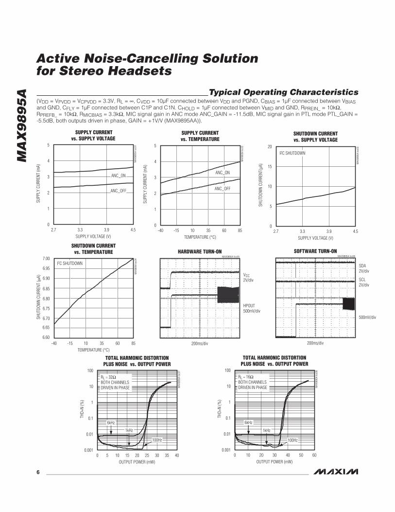
Typical Operating Characteristics(VDD = VPVDD = VCPVDD = 3.3V, RL = ∞, CVDD = 10µF connected between VDD and PGND, CBIAS = 1µF connected between VBIASand GND, CFLY = 1µF connected between C1P and C1N. CHOLD = 1µF connected between VMID and GND, RPREIN_ = 10kΩ,RPREFB_ = 10kΩ, RMICBIAS = 3.3kΩ, MIC signal gain in ANC mode ANC_GAIN = -11.5dB, MIC signal gain in PTL mode PTL_GAIN =-5.5dB, both outputs driven in phase, GAIN = +1V/V (MAX9895AA)).
SUPPLY CURRENTvs. SUPPLY VOLTAGE
MAX
9895
A to
c01
SUPPLY VOLTAGE (V)
SUPP
LY C
URRE
NT (m
A)
3.93.3
1
2
3
4
5
02.7 4.5
ANC_OFF
ANC_ON
SUPPLY CURRENTvs. TEMPERATURE
MAX
9895
A to
c02
TEMPERATURE (°C)
SUPP
LY C
URRE
NT (m
A)
603510-15
1
2
3
4
5
0-40 85
ANC_ON
ANC_OFF
SHUTDOWN CURRENTvs. SUPPLY VOLTAGE
MAX
9895
A to
c03
SHUT
DOW
N CU
RREN
T(µA
)
5
10
15
20
0
SUPPLY VOLTAGE (V)
3.93.32.7 4.5
I2C SHUTDOWN
SHUTDOWN CURRENTvs. TEMPERATURE
MAX
9895
A to
c04
TEMPERATURE (°C)
SHUT
DOW
N CU
RREN
T (µ
A)
603510-15
6.70
6.80
6.90
7.00
6.60
6.75
6.85
6.95
6.65
-40 85
I2C SHUTDOWN
HARDWARE TURN-ONMAX9895A toc05
HPOUT500mV/div
VCC2V/div
200ms/div
SOFTWARE TURN-ONMAX9895A toc06
500mV/div
SDA2V/div
SCL2V/div
200ms/div
TOTAL HARMONIC DISTORTIONPLUS NOISE vs. OUTPUT POWER
MAX
9895
A to
c07
OUTPUT POWER (mW)
THD+
N (%
)
3530252015105
0.01
0.1
1
10
100
0.0010 40
RL = 32IBOTH CHANNELSDRIVEN IN PHASE
6kHz
100Hz
1kHz
OUTPUT POWER (mW)
50403020100 60
TOTAL HARMONIC DISTORTIONPLUS NOISE vs. OUTPUT POWER
MAX
9895
A to
c08
RL = 16IBOTH CHANNELSDRIVEN IN PHASE
THD+
N (%
)
0.01
0.1
1
10
100
0.001
6kHz
100Hz
1kHz
TOTAL HARMONIC DISTORTIONPLUS NOISE vs. FREQUENCY
MAX
9895
A to
c09
FREQUENCY (Hz)
10,0001000100
0.01
0.1
1
0.00110 100,000
RL = 32IBOTH CHANNELSDRIVEN IN PHASE
THD+
N (%
)
5mW
15mW
MA
X9
89
5A
Active Noise-Cancelling Solutionfor Stereo Headsets
_______________________________________________________________________________________ 7
TOTAL HARMONIC DISTORTIONPLUS NOISE vs. FREQUENCY
MAX
9895
A to
c10
FREQUENCY (Hz)
10,0001000100
0.01
0.1
1
0.00110 100,000
RL = 16IBOTH CHANNELSDRIVEN IN PHASE
THD+
N (%
)
15mW
30mW
POWER-SUPPLY REJECTION RATIO
MAX
9895
A to
c11
FREQUENCY (Hz)
PSRR
(dB)
10k1k100
-40
-50
-60
-70
-10
-20
-30
0
-8010 100k
VCC = 3.3V ±100mVP-P
ANC_ON
ANC_OFF
POWER-SUPPLY REJECTION RATIO
MAX
9895
A to
c12
FREQUENCY (Hz)
PSRR
(dB)
1k 10k100
-60
-50
-80
-70
-10
-20
-30
-40
0
-9010 100k
VCC = -3.3V ±100mVP-P
PTL
CROSSTALK vs. FREQUENCY
MAX
9895
A to
c13
CROS
STAL
K (d
B)
-60
-50
-40
-30
-20
-10
0
-70
FREQUENCY (Hz)
10,000100010010 100,000
RL = 32I, POUT = 10mW
OUTPUT SPECTRUM vs. FREQUENCY
MAX
9895
A to
c14
FREQUENCY (Hz)
OUTP
UT S
PECT
RUM
(dBV
)
6k 8k 10k 12k 14k 16k 18k4k2k
-80
-120
-100
-20
-40
-60
0
-1400 20k
VOUT = -60dBV
Typical Operating Characteristics (continued)(VDD = VPVDD = VCPVDD = 3.3V, RL = ∞, CVDD = 10µF connected between VDD and PGND, CBIAS = 1µF connected between VBIASand GND, CFLY = 1µF connected between C1P and C1N. CHOLD = 1µF connected between VMID and GND, RPREIN_ = 10kΩ,RPREFB_ = 10kΩ, RMICBIAS = 3.3kΩ, MIC signal gain in ANC mode ANC_GAIN = -11.5dB, MIC signal gain in PTL mode PTL_GAIN =-5.5dB, both outputs driven in phase, GAIN = +1V/V (MAX9895AA)).
MA
X9
89
5A
Active Noise-Cancelling Solutionfor Stereo Headsets
8 _______________________________________________________________________________________
Typical Operating Characteristics (continued)(VDD = VPVDD = VCPVDD = 3.3V, RL = ∞, CVDD = 10µF connected between VDD and PGND, CBIAS = 1µF connected between VBIASand GND, CFLY = 1µF connected between C1P and C1N. CHOLD = 1µF connected between VMID and GND, RPREIN_ = 10kΩ,RPREFB_ = 10kΩ, RMICBIAS = 3.3kΩ, MIC signal gain in ANC mode ANC_GAIN = -11.5dB, MIC signal gain in PTL mode PTL_GAIN =-5.5dB, both outputs driven in phase, GAIN = +1V/V (MAX9895A)).
MICBIAS POWER-SUPPLYREJECTION RATIO
MAX
9895
A to
c19
FREQUENCY (Hz)
PSRR
(dB)
10,0001000100
-70
-60
-50
-40
-30
-20
-10
0
-8010 100,000
VCC = 3.3V ± 100mVP-PPTL MODEALL BYPASS CAPSREMOVED
MICIN INPUT HEADROOMvs. SUPPLY VOLTAGE
MAX
9895
A to
c20
SUPPLY VOLTAGE (V)
INPU
T HE
ADRO
OM (V
P-P)
3.93.3
100
200
300
400
500
600
02.7 4.5
1%THD, 5V/V EXTERNAL GAIN
TOTAL OUTPUT POWER vs.SUPPLY VOLTAGE
MAX
9895
A to
c17
SUPPLY VOLTAGE (V)
OUTP
UT P
OWER
(mW
)
4.34.12.9 3.1 3.3 3.73.5 3.9
10
20
30
40
50
60
70
80
02.7 4.5
1% THD + N
RL = 32I,BOTH CHANNELSDRIVEN IN PHASE
10% THD + N
OUTPUT POWERvs. SUPPLY VOLTAGE
MAX
9895
A to
c18
SUPPLY VOLTAGE (V)
OUTP
UT P
OWER
(mW
)
4.34.12.9 3.1 3.3 3.73.5 3.9
20
40
60
80
100
120
140
160
02.7 4.5
1% THD + N
RL = 16I,BOTH CHANNELSDRIVEN IN PHASE
10% THD + N
OUTPUT POWERvs. LOAD RESISTANCE
MAX
9895
A to
c16
LOAD RESISTANCE (Ω)
OUTP
UT P
OWER
(mW
)
908060 7020 30 40 5010
10
20
30
40
50
60
70
80
90
100
00 100
1% THD + N
BOTH CHANNELSDRIVEN IN PHASE
10% THD + N
POWER DISSIPATION vs. OUTPUT POWER
MAX
9895
A to
c15
OUTPUT POWER (mW)
POW
ER D
ISSI
PATI
ON (m
W)
908010 20 30 50 6040 70
10
20
30
40
50
60
70
80
00 100
RL = 32I
RL = 16I
BOTH CHANNELSDRIVEN IN PHASE,SIGNAL APPLIED ONLINEIN
MA
X9
89
5A
Active Noise-Cancelling Solutionfor Stereo Headsets
_______________________________________________________________________________________ 9
Pin DescriptionPIN
TQFN WLPNAME FUNCTION
1 A6 SPR1_L Left-Channel Signal Processing
2 C5 MICOUT_LLeft-Channel Microphone Preamplifier Output. Apply feedback resistor to set inputgain. See the Microphone Output section for more details.
3 B6 MICIN_L Left-Channel Microphone Input
4 C6 MICBIAS Microphone Supply Voltage. Use separate left/right MICBIAS resistors.
5 C4 LINEIN_L Left-Channel Audio Line Input
6 D4 LINEIN_R Right-Channel Audio Line Input
7, 8 D6 GND Signal Ground (Reference for VBIAS, MICBIAS, and LINEIN)
9 E6 MICIN_R Right-Channel Microphone Input
10 D5 MICOUT_RRight-Channel Microphone Preamplifier Output. Apply feedback resistor to set inputgain.
11 F6 SPR1_R Right-Channel Signal Processing
12 E5 SPC1_R Right-Channel Signal Processing
13 F5 SPC2_R Right-Channel Signal Processing
14 E4 SPC3_R Right-Channel Signal Processing
15 F4 SPC4_R Right-Channel Signal Processing
16 E3 SPR2_R Right-Channel Signal Processing
17 F3 VBIASInternal Reference. Bypass VBIAS to GND with a 1µF capacitor. Used for MICIN andLINEIN.
18 E2 SPFC2_R Right-Channel Signal Processing
19 F2 SPFC1_R Right-Channel Signal Processing
20 D2 SPFO_R Right-Channel Signal Processing
21 F1 HPOUT_R Right-Channel Headphone Output
22 VDD
23 PVDD
24
E1
CPVDD
Positive Supply Voltage
25 D1 C1P Charge-Pump Flying Capacitor Positive
26 C1 C1N Charge-Pump Flying Capacitor Negative
27 B1 VMIDCharge-Pump Output Voltage. Connect to common return of headphone. BypassVMID with a 1µF capacitor to PGND.
28 — N.C. No Connection
29 A1 PGND Power Ground
30 D3 SDA/NC-MODEI2C Interface Data Line. Also used as MODE select in hardware mode (SCL = GND).See Table 1.
31 C3 SCL I2C Interface Clock Line. Connect to GND for hardware mode.
32 A2 HPOUT_L Left-Channel Headphone Output
MA
X9
89
5A
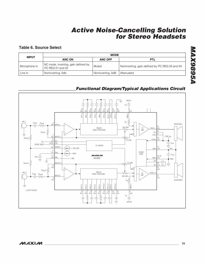
Detailed DescriptionThe MAX9895A is a complete audio subsystem foractive noise-cancelling stereo headsets. The devicefeatures a microphone preamplifier, an analog soundprocessing block, and a headphone amplifier combin-ing to create a simple and very flexible active noise-canceling system. The MAX9895A uses feed-forwardarchitecture, creating a headphone signal that has thesame amplitude, but opposite phase as outside noisethat leaks through the mechanical isolation of the ear-phones. These two signals cancel each other and pro-vide noise suppression at the ear. The device consistsof an ultra-low noise microphone preamplifier to setinput impedance and gain, followed by an analog sig-nal processing block, and a capacitorless headphoneamplifier. The headphone amplifier does not require thelarge output-coupling capacitors used by conventionalsingle-supply headphone amplifiers, and can output33mW into a 16Ω headphone. The product also fea-tures undervoltage lockout and comprehensive click-and-pop suppression circuitry. See the FunctionalDiagram/Typical Applications Circuit for further details.
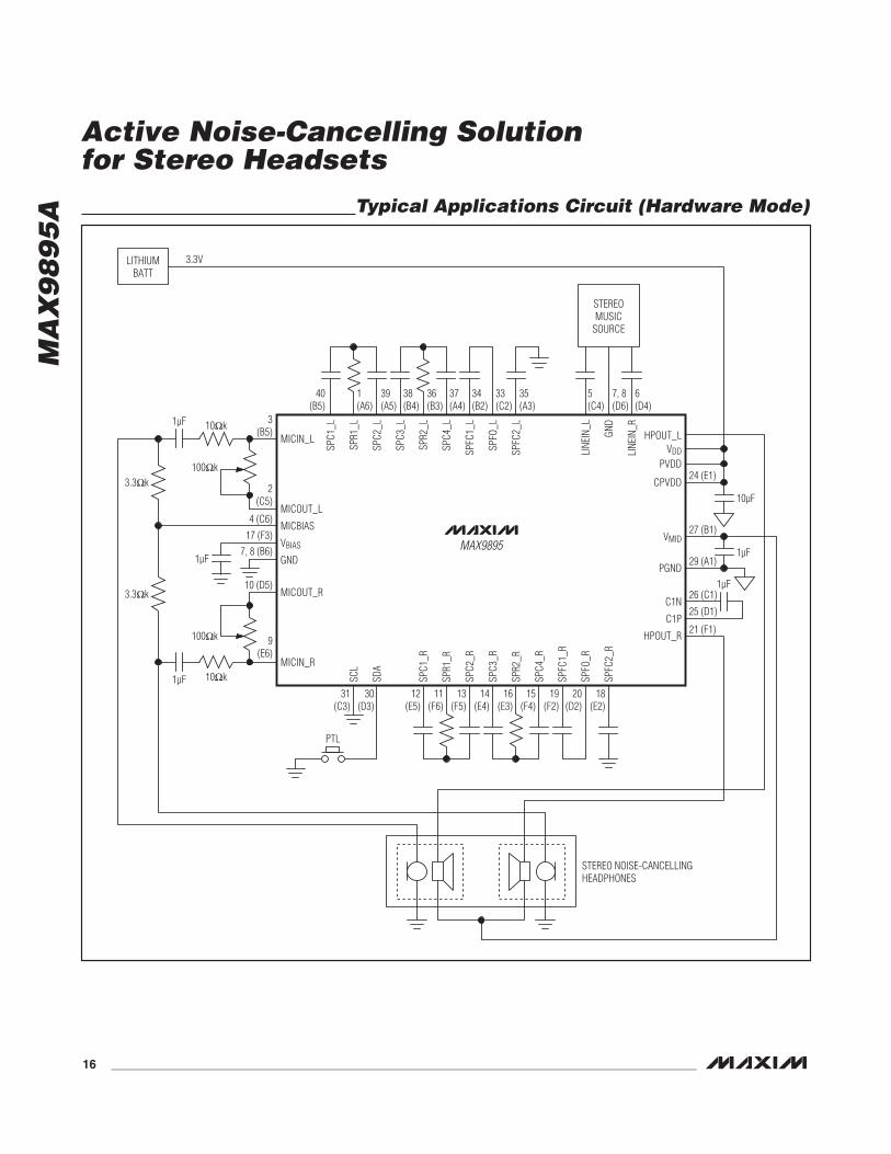
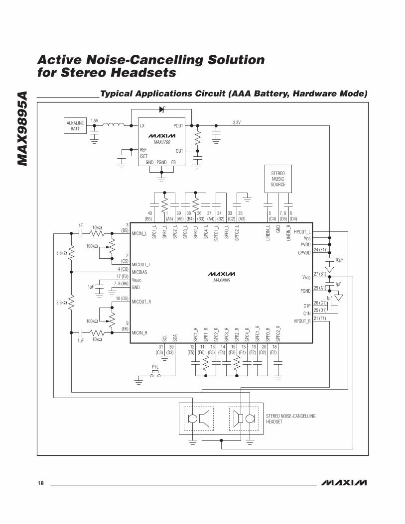
Modes of OperationThe MAX9895A features three modes of operation;active noise canceling (ANC) on or off, and push-to-lis-ten (PTL). The ANC-on mode provides full noise cancel-ing and provides line-input mixing to the headphones.This allows music to be played while noise canceling isoperational. The ANC-off mode disables the micro-phone preamplifiers and noise processing blocks, butallows the line inputs to operate normally. This givesflexibility to the design such that music can still beplayed through the headphones while noise cancelingis inactive.
The PTL mode connects the microphone preamplifierdirectly to the headphone amplifier, bypassing thenoise cancellation, and attenuates the line-input signal.PTL mode gives the user the option of listening to thesurroundings without removing the headphones. SeeTable 1 for hardware mode settings.
Microphone Preamplifier The MAX9895A features an ultra-low noise microphoneinput preamplifier. Using an inverting op amp design withexternal input and feedback resistors allows flexibility insetting input impedance and gain. The microphone gaincan be adjusted in two ways: adjust the feedback resis-tor in the preamplifier stage by use of a potentiometer orsetting I2C registers using a microcontroller to adjust thegain after the analog processing stage.
Microphone Bias SupplyThe MAX9895A provides a low-noise voltage biasdesigned for biasing electret condenser microphones(ECM). The bias output is regulated to 2.5V.
Active Noise-Cancelling Solutionfor Stereo Headsets
10 ______________________________________________________________________________________
Pin DescriptionPIN
TQFN WLPNAME FUNCTION
33 C2 SPFO_L Left-Channel Signal Processing
34 B2 SPFC1_L Left-Channel Signal Processing
35 A3 SPFC2_L Left-Channel Signal Processing
36 B3 SPR2_L Left-Channel Signal Processing
37 A4 SPC4_L Left-Channel Signal Processing
38 B4 SPC3_L Left-Channel Signal Processing
39 A5 SPC2_L Left-Channel Signal Processing
40 B5 SPC1_L Left-Channel Signal Processing
— — EP Exposed Pad. Must be connected to PGND.
SDA LEVEL CONFIGURATION
GND
(PTL Mode) LINEIN_ is attenuated,MICOUT_ signal is passed directly to theheadphone driver without filtering and phasereversal.
Hi-Z ANC on
VDD ANC off (only HP amps are active)
Table 1. Mode Selection (in HardwareMode)
Microphone OutputThe outputs of the microphone preamplifiers are provid-ed to allow for external adjustment of the gain of thepreamplifier and to provide a path for voice transmis-sion (headset) applications.
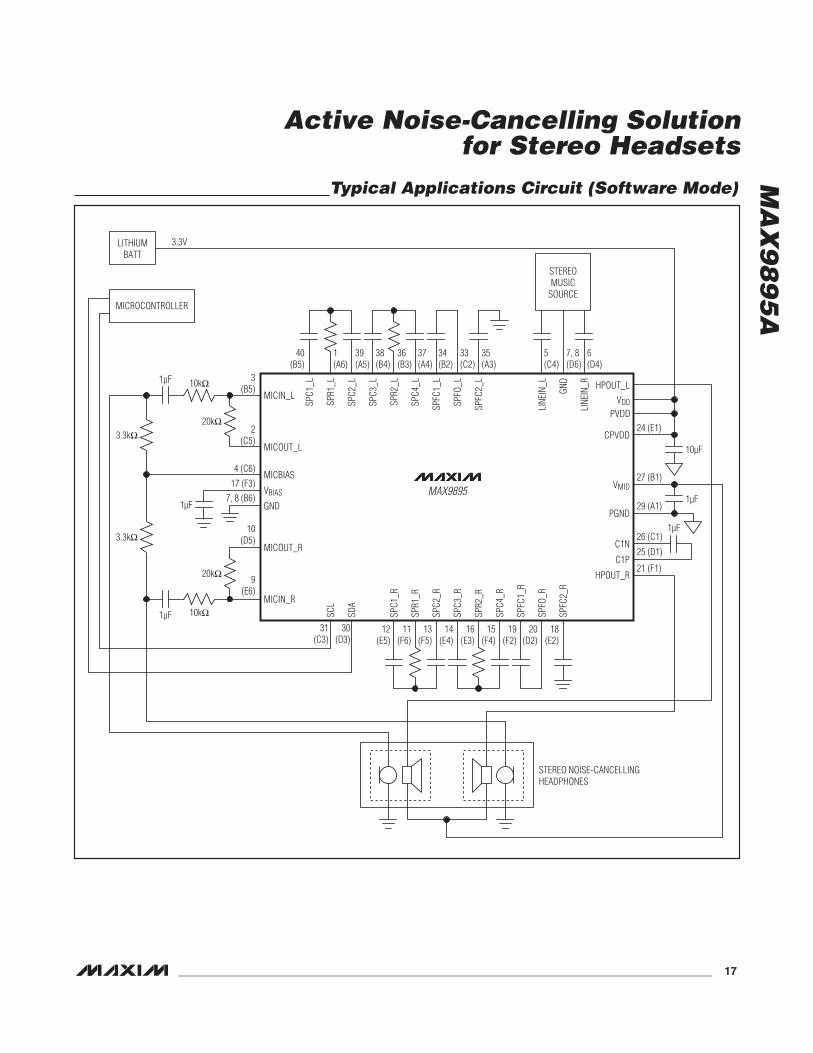
Programmable GainThe second gain stage can be programmed in 0.5dBsteps to compensate for microphone and headphonesensitivity. This requires a microcontroller connected tothe I2C bus, which operates in slave mode. An alternatesolution for gain setting is to add a trim-pot to the feed-back resistor of the microphone preamplifier. See theTypical Application Circuit.
Analog Signal Processing This block creates the noise cancellation signal. Thesignal processing block uses the output of the micro-phone preamp and external components to create aheadphone signal that has the same amplitude, butopposite phase as outside noise that leaks through themechanical isolation of the earphones, so both wavescancel each other. Note: The choice of external com-ponents depends on the headset characteristics.Please contact your local Maxim sales office for moreinformation on determining the proper component val-ues for the Analog Signal Processing section.
Headphone AmplifierThe stereo headphone amplifier is capable of delivering33mW into 16Ω loads and has a gain (line in to head-phone out) of 1V/V for the MAX9895AA. The input to theheadphone amplifier is a linear sum of three signals:line in (external input), mic gain (output of analog signalprocessing block) and PTL gain (ANC bypass).
Unlike conventional single-supply, single-ended ampli-fiers, the MAX9895A headphone amplifier does notneed large DC-blocking caps, as the outputs arereferred to VCC/2, which is the bias output voltage ofthe amplifier. Conventional single-supply headphoneamplifiers require large coupling capacitors to blockthe output DC bias from the headphone. TheMAX9895A architecture uses a high-efficiency chargepump to create an internal midbias supply voltage(VMID). This keeps supply current low and allows theamplifier outputs to be connected directly to the head-phones without the need for these large couplingcapacitors.
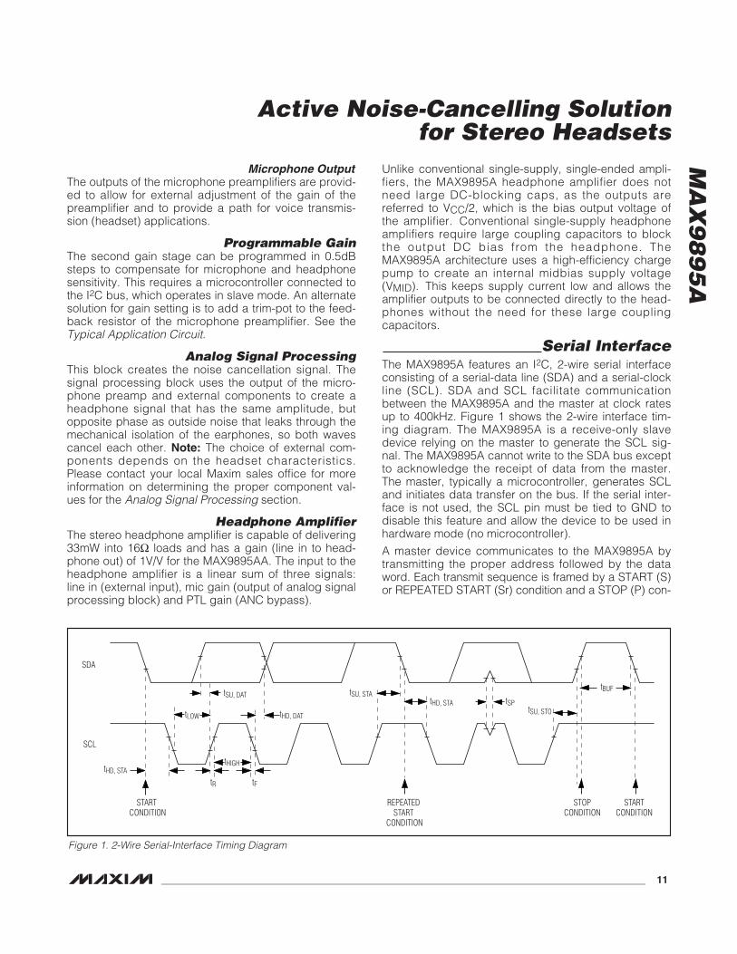
Serial InterfaceThe MAX9895A features an I2C, 2-wire serial interfaceconsisting of a serial-data line (SDA) and a serial-clockline (SCL). SDA and SCL facilitate communicationbetween the MAX9895A and the master at clock ratesup to 400kHz. Figure 1 shows the 2-wire interface tim-ing diagram. The MAX9895A is a receive-only slavedevice relying on the master to generate the SCL sig-nal. The MAX9895A cannot write to the SDA bus exceptto acknowledge the receipt of data from the master.The master, typically a microcontroller, generates SCLand initiates data transfer on the bus. If the serial inter-face is not used, the SCL pin must be tied to GND todisable this feature and allow the device to be used inhardware mode (no microcontroller).
A master device communicates to the MAX9895A bytransmitting the proper address followed by the dataword. Each transmit sequence is framed by a START (S)or REPEATED START (Sr) condition and a STOP (P) con-
MA
X9
89
5A
Active Noise-Cancelling Solutionfor Stereo Headsets
______________________________________________________________________________________ 11
SCL
SDA
STARTCONDITION
STOPCONDITION
REPEATED START
CONDITION
START CONDITION
tHD, STA
tSU, STAtHD, STA tSP
tBUF
tSU, STOtLOW
tSU, DAT
tHD, DAT
tHIGH
tR tF
Figure 1. 2-Wire Serial-Interface Timing Diagram
MA
X9
89
5A
dition. Each word transmitted over the bus is 8 bits longand is always followed by an acknowledge clock pulse.
The MAX9895A SDA line operates as both an input andan open-drain output. A pullup resistor, greater than500Ω, is required on the SDA bus. The MAX9895A SCLline operates as an input only. A pullup resistor, greaterthan 500Ω, is required on SCL if there are multiple mas-ters on the bus, or if the master in a single-master sys-tem has an open-drain SCL output. Series resistors inline with SDA and SCL are optional. Series resistorsprotect the digital inputs of the MAX9895A from high-voltage spikes on the bus lines, and minimize crosstalkand undershoot of the bus signals.
Bit TransferOne data bit is transferred during each SCL cycle. Thedata on SDA must remain stable during the high periodof the SCL pulse. Changes in SDA while SCL is highare control signals (see the START and STOPConditions section). SDA and SCL idle high when theI2C bus is not busy.
START and STOP ConditionsSDA and SCL idle high when the bus is not in use. Amaster device initiates communication by issuing aSTART (S) condition. A START condition is a high-to-lowtransition on SDA with SCL high. A STOP (P) condition isa low-to-high transition on SDA while SCL is high (Figure2). A START condition from the master signals the begin-ning of transmission to the MAX9895A. The master termi-nates transmission and frees the bus by issuing a STOPcondition. The bus remains active if a REPEATED START(Sr) condition is generated instead of a STOP condition.
Early STOP ConditionsThe MAX9895A recognizes a STOP condition at anypoint during data transmission except if the STOP condi-tion occurs in the same high pulse as a START condition.
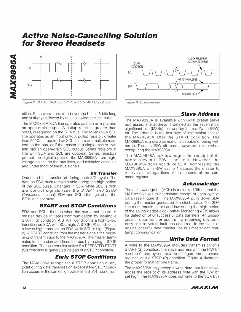
Slave AddressThe MAX9895A is available with 0x40 preset slaveaddresses. The address is defined as the seven mostsignificant bits (MSBs) followed by the read/write (R/W)bit. The address is the first byte of information sent tothe MAX9895A after the START condition. TheMAX9895A is a slave device only capable of being writ-ten to. The sent R/W bit must always be a zero whenconfiguring the MAX9895A.
The MAX9895A acknowledges the receipt of itsaddress even if R/W is set to 1. However, theMAX9895A does not drive SDA. Addressing theMAX9895A with R/W set to 1 causes the master toreceive all 1s regardless of the contents of the com-mand register.
AcknowledgeThe acknowledge bit (ACK) is a clocked 9th bit that theMAX9895A uses to handshake receipt of each byte ofdata (see Figure 3). The MAX9895A pulls down SDAduring the master-generated 9th clock pulse. The SDAline must remain stable and low during the high periodof the acknowledge clock pulse. Monitoring ACK allowsfor detection of unsuccessful data transfers. An unsuc-cessful data transfer occurs if a receiving device isbusy or if a system fault has occurred. In the event ofan unsuccessful data transfer, the bus master can reat-tempt communication.
Write Data FormatA write to the MAX9895A includes transmission of aSTART (S) condition, the slave address with the R/W bitreset to 0, one byte of data to configure the commandregister, and a STOP (P) condition. Figure 4 illustratesthe proper format for one frame.
The MAX9895A only accepts write data, but it acknowl-edges the receipt of its address byte with the R/W bitset high. The MAX9895A does not write to the SDA bus
Active Noise-Cancelling Solutionfor Stereo Headsets
12 ______________________________________________________________________________________
SCL
SDA
S Sr P
Figure 2. START, STOP, and REPEATED START Conditions
1SCL
STARTCONDITION
SDA
2 8 9
CLOCK PULSE FORACKNOWLEDGMENT
ACKNOWLEDGE
NOT ACKNOWLEDGE
Figure 3. Acknowledge
in the event that the R/W bit is set high. Subsequently,the master reads all 1s from the MAX9895A. Alwaysreset the R/W bit to 0 to avoid this situation.
I2C-Enabled Software ModeThe MAX9895A can operate with or without an externalmicrocontroller (µC). When a µC is present, commandsare sent through the I2C protocol (SCL, SDA).
I2C-Disabled Hardware ModeBy tying SCL to ground, the I2C interface is disabledand the device operates in hardware mode. In thiscase, the SDA pin operates as a MODE select. Table 1shows different configurations with the SDA level.
Application InformationInput-Coupling Capacitor
The input capacitor (CIN), in conjunction with the inputresistor (RIN), forms a highpass filter that removes theDC bias from an incoming signal (see the FunctionalDiagram/Typical Applications Circuit). The AC-couplingcapacitor allows the device to bias the signal to an opti-mum DC level. Assuming zero-source impedance, the-3dB point of the highpass filter is given by:
Choose the CIN so that f-3dB is well below the lowestfrequency of interest. Setting f-3dB too high affects the
device’s low-frequency response. Use capacitorswhose dielectrics have low-voltage coefficients, suchas tantalum or aluminum electrolytic. Capacitors withhigh-voltage coefficients, such as ceramics, can resultin increased distortion at low frequencies.
Apply same method for microphone input-coupling capac-itor (CPREIN_). The RIN for microphone input is RPREIN_.
Setting the GainsThe gains of the microphone input preamplifiers are setthrough the feedback using the following equation:
AV (V/V) = -(RF/RIN)
In stand-alone control mode, the internal gain stage forMIC GAIN is fixed at 11.5dB and the PTL GAIN stage isfixed at -5.5dB. In software control mode (I2C mode),the internal gain stage stages, MIC GAIN and PTLGAIN, are programmable through the I2C registers. Seethe Serial Interface section for more information.
The LINE IN and HEADPHONE AMP stages each havefixed voltage gain of 0dB.
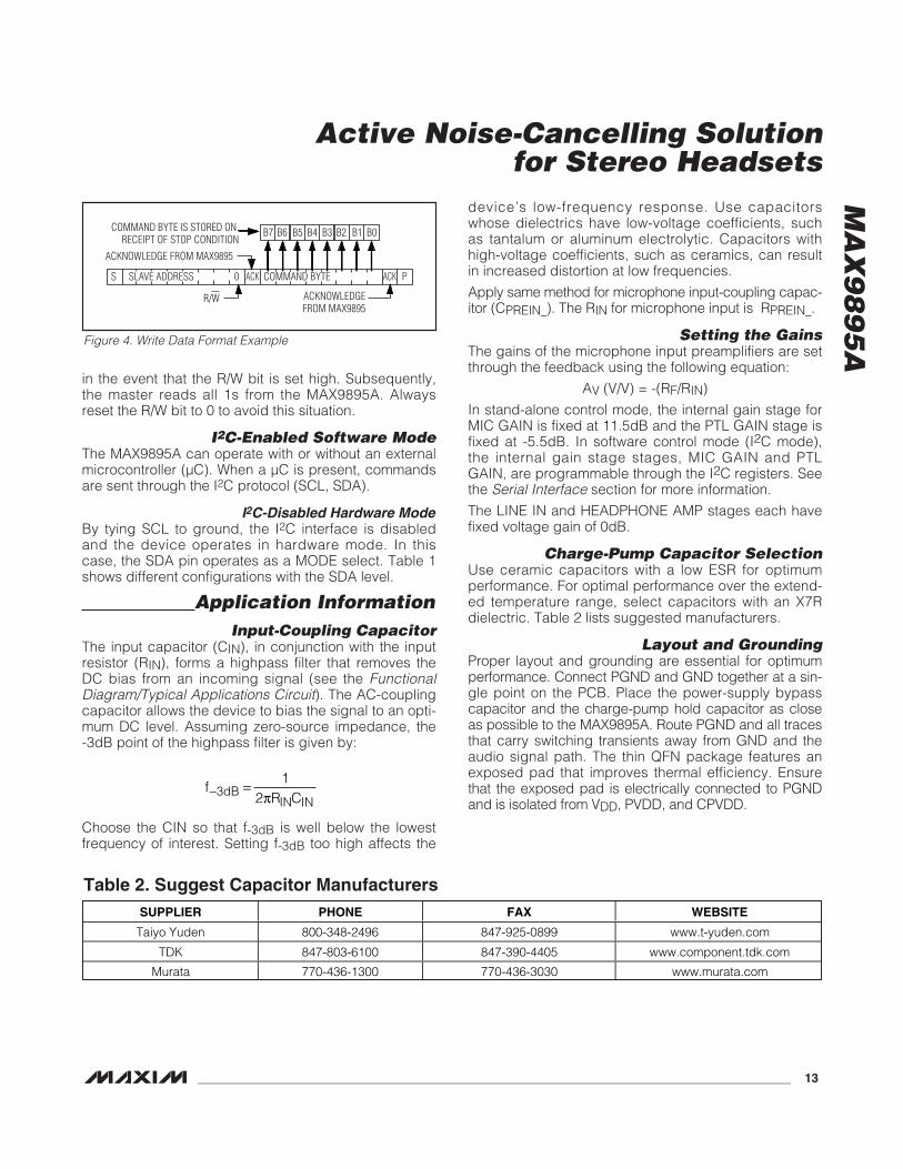
Charge-Pump Capacitor SelectionUse ceramic capacitors with a low ESR for optimumperformance. For optimal performance over the extend-ed temperature range, select capacitors with an X7Rdielectric. Table 2 lists suggested manufacturers.
Layout and GroundingProper layout and grounding are essential for optimumperformance. Connect PGND and GND together at a sin-gle point on the PCB. Place the power-supply bypasscapacitor and the charge-pump hold capacitor as closeas possible to the MAX9895A. Route PGND and all tracesthat carry switching transients away from GND and theaudio signal path. The thin QFN package features anexposed pad that improves thermal efficiency. Ensurethat the exposed pad is electrically connected to PGNDand is isolated from VDD, PVDD, and CPVDD.
fR CdB
IN IN− =3
12π
MA
X9
89
5A
Active Noise-Cancelling Solutionfor Stereo Headsets
______________________________________________________________________________________ 13
S ACK0
ACKNOWLEDGE FROM MAX9895
R/W ACKNOWLEDGEFROM MAX9895
B7 B6 B5 B4 B3 B2COMMAND BYTE IS STORED ON RECEIPT OF STOP CONDITION
ACK P
B1 B0
SLAVE ADDRESS COMMAND BYTE
Figure 4. Write Data Format Example
SUPPLIER PHONE FAX WEBSITE
Taiyo Yuden 800-348-2496 847-925-0899 www.t-yuden.com
TDK 847-803-6100 847-390-4405 www.component.tdk.com
Murata 770-436-1300 770-436-3030 www.murata.com
Table 2. Suggest Capacitor Manufacturers
MA
X9
89
5A
Active Noise-Cancelling Solutionfor Stereo Headsets
14 ______________________________________________________________________________________
ADDRESS TYPE POR NAME 7 6 5 4 3 2 1 0
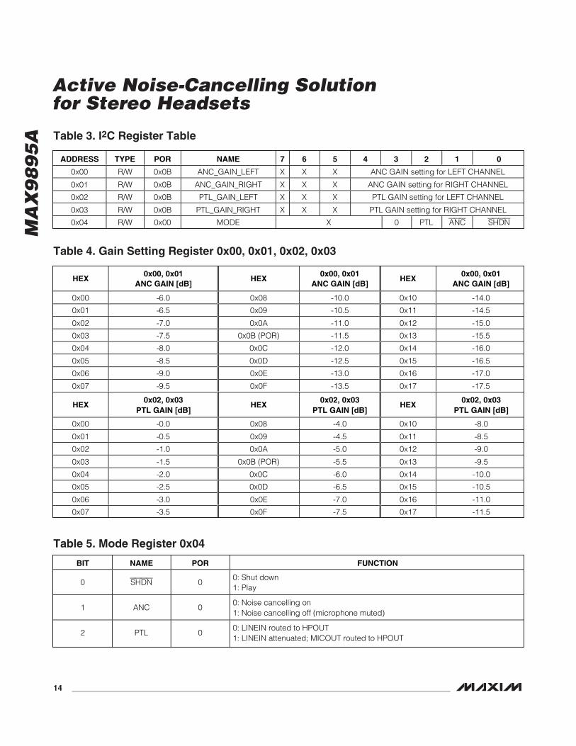
0x00 R/W 0x0B ANC_GAIN_LEFT X X X ANC GAIN setting for LEFT CHANNEL
0x01 R/W 0x0B ANC_GAIN_RIGHT X X X ANC GAIN setting for RIGHT CHANNEL
0x02 R/W 0x0B PTL_GAIN_LEFT X X X PTL GAIN setting for LEFT CHANNEL
0x03 R/W 0x0B PTL_GAIN_RIGHT X X X PTL GAIN setting for RIGHT CHANNEL
0x04 R/W 0x00 MODE X 0 PTL ANC SHDN
Table 3. I2C Register Table
HEX0x00, 0x01
ANC GAIN [dB]HEX
0x00, 0x01ANC GAIN [dB]
HEX0x00, 0x01
ANC GAIN [dB]
0x00 -6.0 0x08 -10.0 0x10 -14.0
0x01 -6.5 0x09 -10.5 0x11 -14.5
0x02 -7.0 0x0A -11.0 0x12 -15.0
0x03 -7.5 0x0B (POR) -11.5 0x13 -15.5
0x04 -8.0 0x0C -12.0 0x14 -16.0
0x05 -8.5 0x0D -12.5 0x15 -16.5
0x06 -9.0 0x0E -13.0 0x16 -17.0
0x07 -9.5 0x0F -13.5 0x17 -17.5
HEX0x02, 0x03
PTL GAIN [dB]HEX
0x02, 0x03PTL GAIN [dB]
HEX0x02, 0x03
PTL GAIN [dB]
0x00 -0.0 0x08 -4.0 0x10 -8.0
0x01 -0.5 0x09 -4.5 0x11 -8.5
0x02 -1.0 0x0A -5.0 0x12 -9.0
0x03 -1.5 0x0B (POR) -5.5 0x13 -9.5
0x04 -2.0 0x0C -6.0 0x14 -10.0
0x05 -2.5 0x0D -6.5 0x15 -10.5
0x06 -3.0 0x0E -7.0 0x16 -11.0
0x07 -3.5 0x0F -7.5 0x17 -11.5
Table 4. Gain Setting Register 0x00, 0x01, 0x02, 0x03
BIT NAME POR FUNCTION
0 SHDN 00: Shut down1: Play
1 ANC 00: Noise cancelling on1: Noise cancelling off (microphone muted)
2 PTL 00: LINEIN routed to HPOUT1: LINEIN attenuated; MICOUT routed to HPOUT
Table 5. Mode Register 0x04
MA
X9
89
5A
Active Noise-Cancelling Solutionfor Stereo Headsets
______________________________________________________________________________________ 15
SDA/NC_MODE
ANALOGSIGNAL PROCESSING
CHARGEPUMP
I2C CONTROL
ANALOGSIGNAL PROCESSING
GND
VBIAS
MIC_BIAS
LINE IN R
HEADPHONE L
HEADPHONE R
PVDD, VDD
VMID
PGND
MIC_L
MIC_R
PTL GAIN
PTL GAIN
ANC GAIN
ANC GAIN
HPAMP
40(B5)
SPC1
_LSP
C1_R
SPC2
_R
SPC3
_R
SPR2
_R
SPR1
_RSP
R1_L
SPC3
_L
SPR2
_L
SPC4
_L
SPFC
1_L
SPFC
2_L
SPFO
_L
SPC2
_L
1(A6)
39(A5)
38(B4)
36(B3)
37(A4)
34(B2)
35(A3)
33(C2)
12(E5)
13(F5)
14(E4)
16(E3)
15(F4)
19(F2)
18(E2)
20(D2)
6(D4)
11(F6)
21(F1)
25(D1)
26(C1)
28, 29(A1)
27(B1)
32(A2)
22
23
3(B6)
2(C5)
31(C3)
30 (D3)4
(C6)
17(F3)
7, 8(D6)
10(D5)
9(E6)
MICIN_R
MICOUT_R
24(E1)
( ) WLPP PACKAGE
CIN
RIN
CPREIN
CPREIN
RPREINL
RPREFBL
RMICBIAS
RMICBIAS
RPREINR
RPREFBR
CBIAS
CFLY
CHOLD
CVDD
HPAMP
SCL
MAX9895
LINE IN L
5(C4)
CIN
RIN
LINE
IN_LHPOUT_L
CPVDD
VMID
PGND
HPOUT_R
CIN
CIP
VDD
PVDD
LINE
IN_R
SPFC
2_R
SPFO
_R
SPFC
1_R
SPFC
4_R
GND
VBIAS
MICBIAS
SDA
SCL
MICOUT_L
MICIN_L
Functional Diagram/Typical Applications Circuit
MODEINPUT
ANC ON ANC OFF PTL
Microphone InNC mode, inverting, gain defined byI2C REG 01 and 02
Muted Noninverting, gain defined by I2C REG 03 and 04
Line In Noninverting, 0db Noninverting, 0dB Attenuated
Table 6. Source Select
MA
X9
89
5A
Active Noise-Cancelling Solutionfor Stereo Headsets
16 ______________________________________________________________________________________
MAX9895
MICIN_L
MICBIAS
MICOUT_L
MICOUT_R
STEREO NOISE-CANCELLINGHEADPHONES
GND
VBIAS
SPFC
2_R
SCL
SDA
1µF 10Ik
MICIN_R
1µF 10Ik
PTL
100Ik
100Ik
3.3Ik
3.3Ik
SPC1
_L
SPR1
_L
SPC2
_L
3.3VLITHIUMBATT
STEREOMUSIC
SOURCE
SPC3
_L
SPR2
_L
SPFC
1_L
SPFO
_L
SPFC
2_L
LINE
IN_L
SPFO
_R
SPFC
1_R
SPC4
_R
GND
LINE
IN_R
SPC4
_L
SPR2
_R
SPC3
_R
HPOUT_L
CPVDD
PVDDVDD
HPOUT_R
C1P
1µF
10µF
VMID
1µF
PGND
C1N
SPC2
_R
SPR1
_R
SPC1
_R
1µF
6(D4)
24 (E1)
27 (B1)
29 (A1)
26 (C1)
25 (D1)
21 (F1)
7, 8(D6)
5(C4)
35(A3)
33(C2)
34(B2)
37(A4)
36(B3)
38(B4)
39(A5)
1(A6)
40(B5)
3(B5)
2(C5)
4 (C6)
17 (F3)
7, 8 (B6)
10 (D5)
9(E6)
31(C3)
30(D3)
12(E5)
11(F6)
13(F5)
14(E4)
16(E3)
15(F4)
19(F2)
20(D2)
18(E2)
Typical Applications Circuit (Hardware Mode)
MA
X9
89
5A
Active Noise-Cancelling Solutionfor Stereo Headsets
______________________________________________________________________________________ 17
MICIN_L
MICBIAS
MICOUT_L
MICOUT_R
STEREO NOISE-CANCELLINGHEADPHONES
GND
VBIAS
SPFC
2_R
SCL
SDA
1µF 10kI
MICIN_R
1µF 10kI
20kI
20kI
3.3kI
3.3kI
SPC1
_L
SPR1
_L
SPC2
_L
3.3VLITHIUMBATT
MICROCONTROLLER
SPC3
_L
SPR2
_L
SPFC
1_L
SPFO
_L
SPFC
2_L
LINE
IN_L
SPFO
_R
SPFC
1_R
SPC4
_R
GND
LINE
IN_R
SPC4
_L
SPR2
_R
SPC3
_R
HPOUT_L
CPVDD
HPOUT_R
C1P
1µF
10µF
VMID
1µFPGND
C1N
SPC2
_R
SPR1
_R
SPC1
_R
31(C3)
30(D3)
12(E5)
11(F6)
13(F5)
14(E4)
16(E3)
15(F4)
19(F2)
20(D2)
18(E2)
1µFMAX9895
STEREOMUSIC
SOURCE
6(D4)
7, 8(D6)
5(C4)
35(A3)
33(C2)
34(B2)
37(A4)
36(B3)
38(B4)
39(A5)
1(A6)
40(B5)
24 (E1)
27 (B1)
29 (A1)
26 (C1)
25 (D1)
21 (F1)
PVDDVDD
3(B5)
2(C5)
4 (C6)
17 (F3)
7, 8 (B6)
10(D5)
9(E6)
Typical Applications Circuit (Software Mode)
MA
X9
89
5A
Active Noise-Cancelling Solutionfor Stereo Headsets
18 ______________________________________________________________________________________
MAX9895
MAX1760
MICIN_L
MICBIAS
MICOUT_L
MICOUT_R
STEREO NOISE-CANCELLINGHEADSET
GND
VBIASSP
FC2_
R
SCL
SDA
GND PGND FB
1F 10kI
MICIN_R
1µF 10kI
100kI
100kI
3.3kI
3.3kI
SPC1
_L
SPR1
_L
SPC2
_L
1.5V 3.3VALKALINEBATT LX
REFISET
POUT
SPC3
_L
SPR2
_L
SPFC
1_L
SPFO
_L
SPFC
2_L
LINE
IN_L
SPFO
_R
SPFC
1_R
SPC4
_R
GND
LINE
IN_R
SPC4
_L
SPR2
_R
SPC3
_R
CPVDD
HPOUT_R
C1N
1µF
24 (E1)
27 (B1)
29 (A1)
26 (C1)
25 (D1)
21 (F1)
10µF
VMID
1µFPGND
C1P
SPC2
_R
SPR1
_R
SPC1
_R
OUT
1µF
STEREOMUSIC
SOURCE
6(D4)
7, 8(D6)
5(C4)
35(A3)
33(C2)
34(B2)
37(A4)
36(B3)
38(B4)
39(A5)
1(A6)
40(B5)
HPOUT_L
PVDDVDD
PTL
31(C3)
30(D3)
12(E5)
11(F6)
13(F5)
14(E4)
16(E3)
15(F4)
19(F2)
20(D2)
18(E2)
3(B5)
2(C5)
4 (C6)
17 (F3)
7, 8 (B6)
10 (D5)
9(E6)
Typical Applications Circuit (AAA Battery, Hardware Mode)
MA
X9
89
5A
Active Noise-Cancelling Solutionfor Stereo Headsets
______________________________________________________________________________________ 19
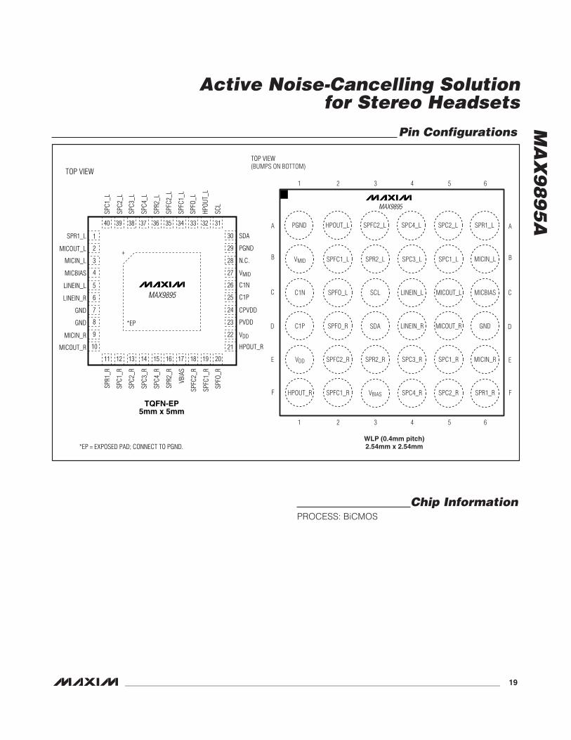
WLP (0.4mm pitch)2.54mm x 2.54mm
A
B
C
MAX9895
D
F
E
TOP VIEW(BUMPS ON BOTTOM)
PGND HPOUT_L SPFC2_L SPC4_L SPC2_L SPR1_L
VMID SPFC1_L SPR2_L SPC3_L SPC1_L MICIN_L
C1N SPFO_L SCL LINEIN_L MICOUT_L MICBIAS
C1P SPFO_R SDA LINEIN_R MICOUT_R GND
VDD SPFC2_R SPR2_R SPC3_R SPC1_R MICIN_R
HPOUT_R SPFC1_R VBIAS SPC4_R SPC2_R SPR1_R
A
B
C
D
F
E
2 3 4 5 61
2 3 4 5 61
TQFN-EP5mm x 5mm
TOP VIEW
3536 34 33
1211 13
SPC1
_R
SPC3
_R
SPC4
_R
SPR2
_R
VBIA
S
14
SPR1
_R
SPC4
_L
SPFC
2_L
SPFC
1_L
SPC3
_L
SPC2
_L
SPC1
_L
SPFO
_L
HPOU
T_L
1
2
MICBIAS 4
5
6
7
27
28
29
30
26
24
23
22
LINEIN_L
LINEIN_R
N.C.
VMID
C1N
C1P
SPC2
_R
SPR2
_L
3
25
37
GND CPVDD
383940
GND
MICIN_R
MICOUT_R
PVDD
VDD
HPOUT_R
MICIN_L
32
15
PGNDMICOUT_L
31
16 17 18 19 20
SDA
SPFC
2_R
SPFC
1_R
SPFO
_RSC
L
8
9
10 21
SPR1_L
*EP = EXPOSED PAD; CONNECT TO PGND.
*EP
+
MAX9895
Pin Configurations
Chip InformationPROCESS: BiCMOS
MA
X9
89
5A
Active Noise-Cancelling Solutionfor Stereo Headsets
20 ______________________________________________________________________________________
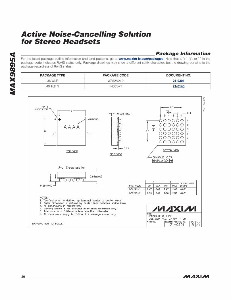
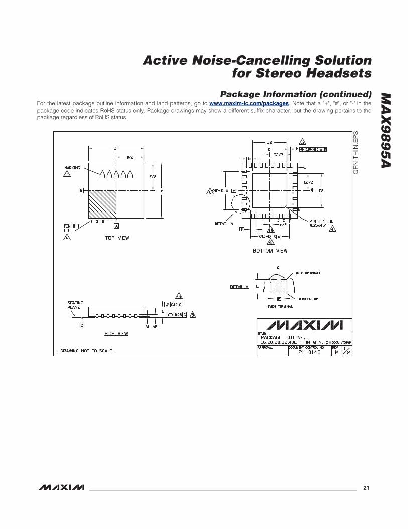
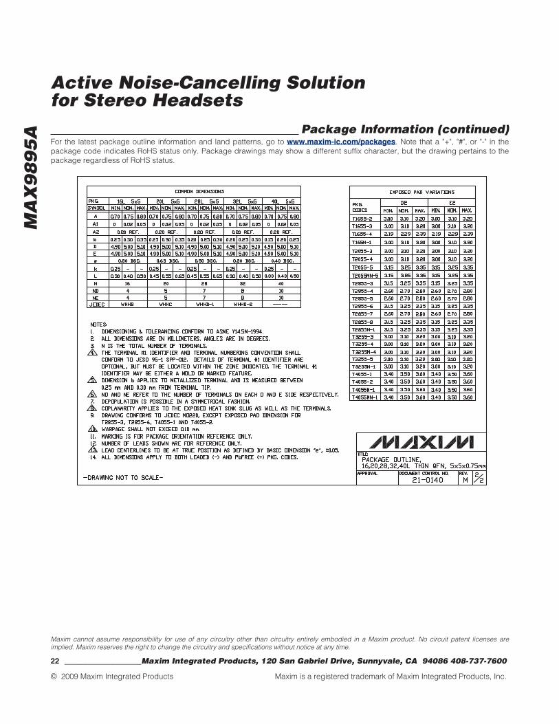
PACKAGE TYPE PACKAGE CODE DOCUMENT NO.
36 WLP W362A2+2 21-0301
40 TQFN T4055+1 21-0140
WLP
PK
G.E
PS
Package InformationFor the latest package outline information and land patterns, go to www.maxim-ic.com/packages. Note that a "+", "#", or "-" in thepackage code indicates RoHS status only. Package drawings may show a different suffix character, but the drawing pertains to thepackage regardless of RoHS status.
MA
X9
89
5A
Active Noise-Cancelling Solutionfor Stereo Headsets
______________________________________________________________________________________ 21
QFN
TH
IN.E
PS
Package Information (continued)For the latest package outline information and land patterns, go to www.maxim-ic.com/packages. Note that a "+", "#", or "-" in thepackage code indicates RoHS status only. Package drawings may show a different suffix character, but the drawing pertains to thepackage regardless of RoHS status.
MA
X9
89
5A
Active Noise-Cancelling Solutionfor Stereo Headsets
Maxim cannot assume responsibility for use of any circuitry other than circuitry entirely embodied in a Maxim product. No circuit patent licenses areimplied. Maxim reserves the right to change the circuitry and specifications without notice at any time.
22 ____________________Maxim Integrated Products, 120 San Gabriel Drive, Sunnyvale, CA 94086 408-737-7600
© 2009 Maxim Integrated Products Maxim is a registered trademark of Maxim Integrated Products, Inc.
Package Information (continued)For the latest package outline information and land patterns, go to www.maxim-ic.com/packages. Note that a "+", "#", or "-" in thepackage code indicates RoHS status only. Package drawings may show a different suffix character, but the drawing pertains to thepackage regardless of RoHS status.