EVALUATION KIT AVAILABLE 500ksps, Low-Power, … · _____ Maxim Integrated Products 1 For pricing,...
28
_______________________________________________________________ Maxim Integrated Products 1 For pricing, delivery, and ordering information, please contact Maxim Direct at 1-888-629-4642, or visit Maxim’s website at www.maxim-ic.com. MAX11661–MAX11666 500ksps, Low-Power, Serial 12-/10-/8-Bit ADCs General Description The MAX11661−MAX11666 are 12-/10-/8-bit, compact, low-power, successive approximation analog-to-digital converters (ADCs). These high-performance ADCs include a high-dynamic range sample-and-hold and a high-speed serial interface. These ADCs accept a full-scale input from 0V to the power supply or to the reference voltage. The MAX11662/MAX11664/MAX11666 feature dual, sin- gle-ended analog inputs connected to the ADC core using a 2:1 MUX. The devices also include a separate supply input for data interface and a dedicated input for reference voltage. In contrast, the single-channel devices generate the reference voltage internally from the power supply. These ADCs operate from a 2.2V to 3.6V supply and consume only 3.3mW. The devices include full power- down mode and fast wake-up for optimal power man- agement and a high-speed 3-wire serial interface. The 3-wire serial interface directly connects to SPI, QSPIK, and MICROWIRE ® devices without external logic. Excellent dynamic performance, low voltage, low power, ease of use, and small package size make these con- verters ideal for portable battery-powered data-acquisi- tion applications, and for other applications that demand low-power consumption and minimal space. These ADCs are available in a 10-pin FMAX ® package, and a 6-pin SOT23 package. These devices operate over the -40NC to +125NC temperature range. Features S 500ksps Conversion Rate, No Pipeline Delay S 12-/10-/8-Bit Resolution S 1-/2-Channel, Single-Ended Analog Inputs S Low-Noise 73dB SNR S Variable I/O: 1.5V to 3.6V (Dual-Channel Only) Allows the Serial Interface to Connect Directly to 1.5V, 1.8V, 2.5V, or 3V Digital Systems S 2.2V to 3.6V Supply Voltage S Low Power 3.3mW Very Low Power Consumption at 8µA/ksps S External Reference Input (Dual-Channel Devices Only) S 1.3µA Power-Down Current S SPI-/QSPI-/MICROWIRE-Compatible Serial Interface S 10-Pin, 3mm x 5mm µMAX Package S 6-Pin, 2.8mm x 2.9mm SOT23 Package S Wide -40NC to +125NC Operation Applications Data Acquisition Portable Data Logging Medical Instrumentation Battery-Operated Systems Communication Systems Automotive Systems 19-5530; Rev 5; 4/12 Note: All devices are specified over the -40°C to +125°C operating temperature range. +Denotes a lead(Pb)-free/RoHS-compliant package. *EP = Exposed pad. /V denotes an automotive qualified part. Ordering Information QSPI is a trademark of Motorola, Inc. MICROWIRE is a registered trademark of National Semiconductor Corp. µMAX is a registered trademark of Maxim Integrated Products, Inc. EVALUATION KIT AVAILABLE PART PIN-PACKAGE BITS NO. OF CHANNELS MAX11661AUT+ 6 SOT23 8 1 MAX11662AUB+ 10 FMAX-EP* 8 2 MAX11663AUT+ 6 SOT23 10 1 MAX11664AUB+ 10 FMAX-EP* 10 2 MAX11665AUT+ 6 SOT23 12 1 MAX11666AUB+ 10 FMAX-EP* 12 2 MAX11666AUB/V+ 10 FMAX-EP* 12 2
Transcript of EVALUATION KIT AVAILABLE 500ksps, Low-Power, … · _____ Maxim Integrated Products 1 For pricing,...

_______________________________________________________________ Maxim Integrated Products 1
For pricing, delivery, and ordering information, please contact Maxim Direct at 1-888-629-4642, or visit Maxim’s website at www.maxim-ic.com.
MA
X1
16
61
–MA
X1
16
66
500ksps, Low-Power, Serial 12-/10-/8-Bit ADCs
General DescriptionThe MAX11661−MAX11666 are 12-/10-/8-bit, compact, low-power, successive approximation analog-to-digital converters (ADCs). These high-performance ADCs include a high-dynamic range sample-and-hold and a high-speed serial interface. These ADCs accept a full-scale input from 0V to the power supply or to the reference voltage.
The MAX11662/MAX11664/MAX11666 feature dual, sin-gle-ended analog inputs connected to the ADC core using a 2:1 MUX. The devices also include a separate supply input for data interface and a dedicated input for reference voltage. In contrast, the single-channel devices generate the reference voltage internally from the power supply.
These ADCs operate from a 2.2V to 3.6V supply and consume only 3.3mW. The devices include full power-down mode and fast wake-up for optimal power man-agement and a high-speed 3-wire serial interface. The 3-wire serial interface directly connects to SPI, QSPIK, and MICROWIRE® devices without external logic.
Excellent dynamic performance, low voltage, low power, ease of use, and small package size make these con-verters ideal for portable battery-powered data-acquisi-tion applications, and for other applications that demand low-power consumption and minimal space.
These ADCs are available in a 10-pin FMAX® package, and a 6-pin SOT23 package. These devices operate over the -40NC to +125NC temperature range.
FeaturesS 500ksps Conversion Rate, No Pipeline Delay
S 12-/10-/8-Bit Resolution
S 1-/2-Channel, Single-Ended Analog Inputs
S Low-Noise 73dB SNR
S Variable I/O: 1.5V to 3.6V (Dual-Channel Only) Allows the Serial Interface to Connect Directly to 1.5V, 1.8V, 2.5V, or 3V Digital Systems
S 2.2V to 3.6V Supply Voltage
S Low Power 3.3mW Very Low Power Consumption at 8µA/ksps
S External Reference Input (Dual-Channel Devices Only)
S 1.3µA Power-Down Current
S SPI-/QSPI-/MICROWIRE-Compatible Serial Interface
S 10-Pin, 3mm x 5mm µMAX Package
S 6-Pin, 2.8mm x 2.9mm SOT23 Package
S Wide -40NC to +125NC Operation
ApplicationsData Acquisition
Portable Data Logging
Medical Instrumentation
Battery-Operated Systems
Communication Systems
Automotive Systems
19-5530; Rev 5; 4/12
Note: All devices are specified over the -40°C to +125°C operating temperature range.+Denotes a lead(Pb)-free/RoHS-compliant package.*EP = Exposed pad./V denotes an automotive qualified part.
Ordering Information
QSPI is a trademark of Motorola, Inc. MICROWIRE is a registered trademark of National Semiconductor Corp. µMAX is a registered trademark of Maxim Integrated Products, Inc.
EVALUATION KIT
AVAILABLE
PART PIN-PACKAGE BITS NO. OF CHANNELS
MAX11661AUT+ 6 SOT23 8 1
MAX11662AUB+ 10 FMAX-EP* 8 2
MAX11663AUT+ 6 SOT23 10 1
MAX11664AUB+ 10 FMAX-EP* 10 2
MAX11665AUT+ 6 SOT23 12 1
MAX11666AUB+ 10 FMAX-EP* 12 2
MAX11666AUB/V+ 10 FMAX-EP* 12 2

2 ______________________________________________________________________________________
MA
X1
16
61
–MA
X1
16
66
500ksps, Low-Power, Serial 12-/10-/8-Bit ADCs
Stresses beyond those listed under “Absolute Maximum Ratings” may cause permanent damage to the device. These are stress ratings only, and functional operation of the device at these or any other conditions beyond those indicated in the operational sections of the specifications is not implied. Exposure to absolute maximum rating conditions for extended periods may affect device reliability.
VDD to GND .............................................................-0.3V to +4VREF, OVDD, AIN1, AIN2, AIN to GND ........-0.3V to the lower of
(VDD + 0.3V) and +4VCS, SCLK, CHSEL, DOUT TO GND ............-0.3V to the lower of
(VOVDD + 0.3V) and +4VAGND to GND ......................................................-0.3V to +0.3VInput/Output Current (all pins) ...........................................50mA
Continuous Power Dissipation (TA = +70NC) 6-Pin SOT23 (derate 8.7mW/NC above +70NC) ...........696mW 10-Pin FMAX (derate 8.8mW/NC above +70NC)........707.3mWOperating Temperature Range ....................... .-40NC to +125NCJunction Temperature .....................................................+150NCStorage Temperature Range ............................ -65NC to +150NCLead Temperature (soldering, 10s) ................................+300NCSoldering Temperature (reflow) ......................................+260NC
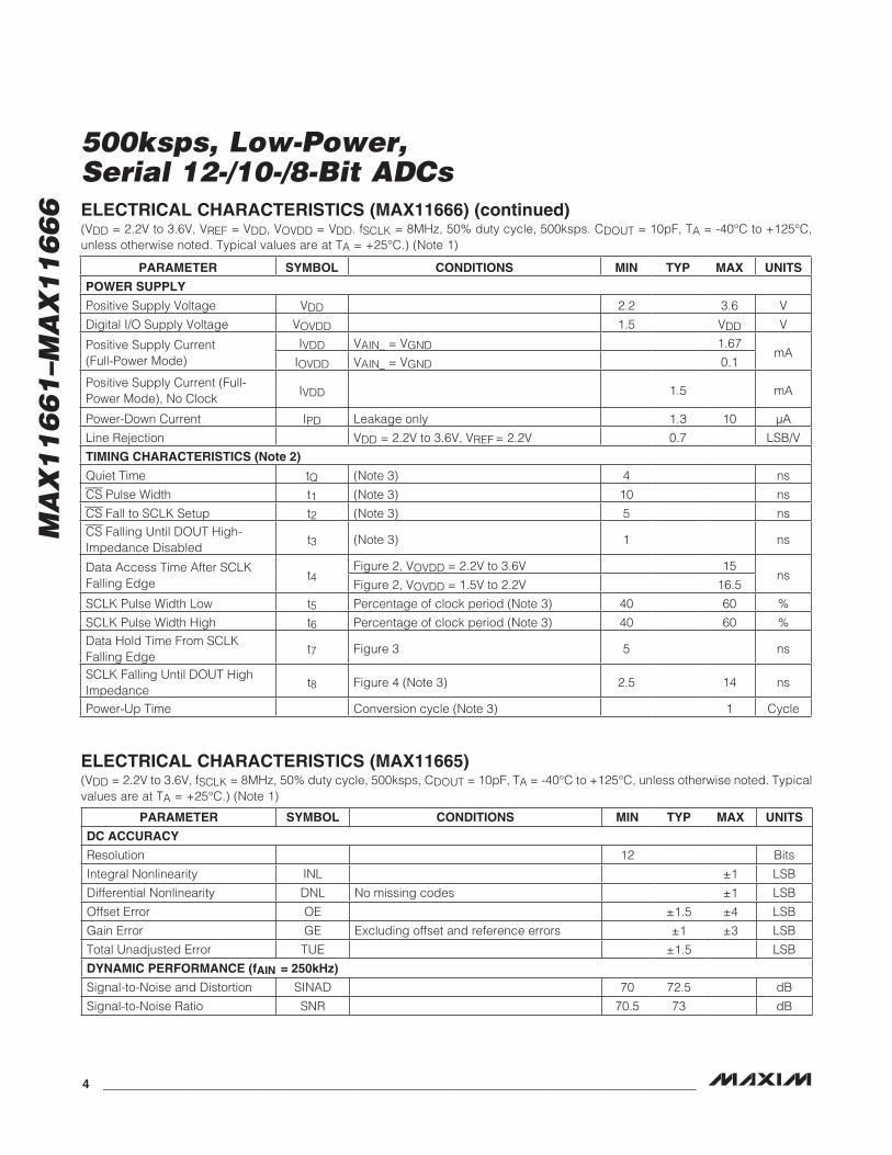
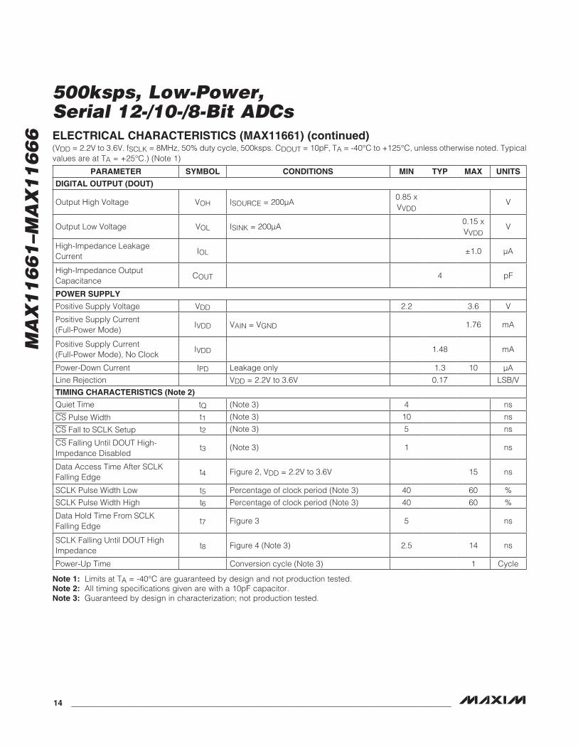
ELECTRICAL CHARACTERISTICS (MAX11666)(VDD = 2.2V to 3.6V, VREF = VDD, VOVDD = VDD. fSCLK = 8MHz, 50% duty cycle, 500ksps. CDOUT = 10pF, TA = -40NC to +125NC, unless otherwise noted. Typical values are at TA = +25NC.) (Note 1)
ABSOLUTE MAXIMUM RATINGS
PARAMETER SYMBOL CONDITIONS MIN TYP MAX UNITS
DC ACCURACY
Resolution 12 Bits
Integral Nonlinearity INL Q1 LSB
Differential Nonlinearity DNL No missing codes Q1 LSB
Offset Error OE Q0.3 Q4 LSB
Gain Error GE Excluding offset and reference errors Q1 Q3 LSB
Total Unadjusted Error TUE Q1 LSB
Channel-to-Channel Offset Matching
Q0.4 LSB
Channel-to-Channel Gain Matching
Q0.05 LSB
DYNAMIC PERFORMANCE (fAIN = 250kHz)
Signal-to-Noise and Distortion SINAD 70 72 dB
Signal-to-Noise Ratio SNR 70.5 72.5 dB
Total Harmonic Distortion THD -85 -74.5 dB
Spurious-Free Dynamic Range SFDR 75.5 85 dB
Intermodulation Distortion IMD f1 = 239.8kHz, f2 = 200.2kHz -84 dB
Full-Power Bandwidth -3dB point 40 MHz
Full-Linear Bandwidth SINAD > 68dB 2.5 MHz
Small-Signal Bandwidth 45 MHz
Crosstalk -90 dB

_______________________________________________________________________________________ 3
MA
X1
16
61
–MA
X1
16
66
500ksps, Low-Power, Serial 12-/10-/8-Bit ADCs
ELECTRICAL CHARACTERISTICS (MAX11666) (continued)(VDD = 2.2V to 3.6V, VREF = VDD, VOVDD = VDD. fSCLK = 8MHz, 50% duty cycle, 500ksps. CDOUT = 10pF, TA = -40NC to +125NC, unless otherwise noted. Typical values are at TA = +25NC.) (Note 1)
PARAMETER SYMBOL CONDITIONS MIN TYP MAX UNITS
CONVERSION RATE
Throughput 5 500 ksps
Conversion Time 1.56 Fs
Acquisition Time tACQ 52 ns
Aperture Delay From CS falling edge 4 ns
Aperture Jitter 15 ps
Serial-Clock Frequency fCLK 0.08 8 MHz
ANALOG INPUT (AIN1, AIN2)
Input Voltage Range VAIN_ 0 VREF V
Input Leakage Current IILA 0.002 Q1 FA
Input Capacitance CAIN_Track 20
pFHold 4
EXTERNAL REFERENCE INPUT (REF)
Reference Input Voltage Range VREF 1VDD + 0.05
V
Reference Input Leakage Current
IILR Conversion stopped 0.005 Q1 FA
Reference Input Capacitance CREF 5 pF
DIGITAL INPUTS (SCLK, CS, CHSEL)
Digital Input High Voltage VIH0.75 x VOVDD
V
Digital Input Low Voltage VIL0.25 x VOVDD
V
Digital Input Hysteresis VHYST0.15 x VOVDD
V
Digital Input Leakage Current IIL Inputs at GND or VDD 0.001 Q1 FA
Digital Input Capacitance CIN 2 pF
DIGITAL OUTPUT (DOUT)
Output High Voltage VOH ISOURCE = 200FA0.85 x VOVDD
V
Output Low Voltage VOL ISINK = 200FA0.15 x VOVDD
V
High-Impedance Leakage Current
IOL Q1.0 FA
High-Impedance Output Capacitance
COUT 4 pF
4 ______________________________________________________________________________________
MA
X1
16
61
–MA
X1
16
66
500ksps, Low-Power, Serial 12-/10-/8-Bit ADCsELECTRICAL CHARACTERISTICS (MAX11666) (continued)(VDD = 2.2V to 3.6V, VREF = VDD, VOVDD = VDD. fSCLK = 8MHz, 50% duty cycle, 500ksps. CDOUT = 10pF, TA = -40NC to +125NC, unless otherwise noted. Typical values are at TA = +25NC.) (Note 1)
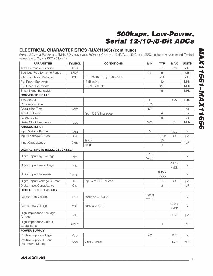
ELECTRICAL CHARACTERISTICS (MAX11665)(VDD = 2.2V to 3.6V, fSCLK = 8MHz, 50% duty cycle, 500ksps, CDOUT = 10pF, TA = -40NC to +125NC, unless otherwise noted. Typical values are at TA = +25NC.) (Note 1)
PARAMETER SYMBOL CONDITIONS MIN TYP MAX UNITS
POWER SUPPLY
Positive Supply Voltage VDD 2.2 3.6 V
Digital I/O Supply Voltage VOVDD 1.5 VDD V
Positive Supply Current (Full-Power Mode)
IVDD VAIN_ = VGND 1.67mA
IOVDD VAIN_ = VGND 0.1
Positive Supply Current (Full-Power Mode), No Clock
IVDD 1.5 mA
Power-Down Current IPD Leakage only 1.3 10 FA
Line Rejection VDD = 2.2V to 3.6V, VREF = 2.2V 0.7 LSB/V
TIMING CHARACTERISTICS (Note 2)
Quiet Time tQ (Note 3) 4 ns
CS Pulse Width t1 (Note 3) 10 ns
CS Fall to SCLK Setup t2 (Note 3) 5 nsCS Falling Until DOUT High-Impedance Disabled
t3 (Note 3) 1 ns
Data Access Time After SCLK Falling Edge
t4Figure 2, VOVDD = 2.2V to 3.6V 15
nsFigure 2, VOVDD = 1.5V to 2.2V 16.5
SCLK Pulse Width Low t5 Percentage of clock period (Note 3) 40 60 %
SCLK Pulse Width High t6 Percentage of clock period (Note 3) 40 60 %Data Hold Time From SCLK Falling Edge
t7 Figure 3 5 ns
SCLK Falling Until DOUT High Impedance
t8 Figure 4 (Note 3) 2.5 14 ns
Power-Up Time Conversion cycle (Note 3) 1 Cycle
PARAMETER SYMBOL CONDITIONS MIN TYP MAX UNITS
DC ACCURACY
Resolution 12 Bits
Integral Nonlinearity INL Q1 LSB
Differential Nonlinearity DNL No missing codes Q1 LSB
Offset Error OE Q1.5 Q4 LSB
Gain Error GE Excluding offset and reference errors Q1 Q3 LSB
Total Unadjusted Error TUE Q1.5 LSB
DYNAMIC PERFORMANCE (fAIN = 250kHz)
Signal-to-Noise and Distortion SINAD 70 72.5 dB
Signal-to-Noise Ratio SNR 70.5 73 dB
_______________________________________________________________________________________ 5
MA
X1
16
61
–MA
X1
16
66
500ksps, Low-Power, Serial 12-/10-/8-Bit ADCs
ELECTRICAL CHARACTERISTICS (MAX11665) (continued)(VDD = 2.2V to 3.6V, fSCLK = 8MHz, 50% duty cycle, 500ksps, CDOUT = 10pF, TA = -40NC to +125NC, unless otherwise noted. Typical values are at TA = +25NC.) (Note 1)
PARAMETER SYMBOL CONDITIONS MIN TYP MAX UNITS
Total Harmonic Distortion THD -85 -76 dB
Spurious-Free Dynamic Range SFDR 77 85 dB
Intermodulation Distortion IMD f1 = 239.8kHz, f2 = 200.2kHz -84 dB
Full-Power Bandwidth -3dB point 40 MHz
Full-Linear Bandwidth SINAD > 68dB 2.5 MHz
Small-Signal Bandwidth 45 MHz
CONVERSION RATE
Throughput 5 500 ksps
Conversion Time 1.56 Fs
Acquisition Time tACQ 52 ns
Aperture Delay From CS falling edge 4 ns
Aperture Jitter 15 ps
Serial Clock Frequency fCLK 0.08 8 MHz
ANALOG INPUT
Input Voltage Range VAIN 0 VDD V
Input Leakage Current IILA 0.002 Q1 FA
Input Capacitance CAINTrack 20
pFHold 4
DIGITAL INPUTS (SCLK, CS, CHSEL)
Digital Input High Voltage VIH0.75 x VVDD
V
Digital Input Low Voltage VIL0.25 x VVDD
V
Digital Input Hysteresis VHYST0.15 x VVDD
V
Digital Input Leakage Current IIL Inputs at GND or VDD 0.001 Q1 FA
Digital Input Capacitance CIN 2 pF
DIGITAL OUTPUT (DOUT)
Output High Voltage VOH ISOURCE = 200FA0.85 x VVDD
V
Output Low Voltage VOL ISINK = 200FA0.15 x VVDD
V
High-Impedance Leakage Current
IOL Q1.0 FA
High-Impedance Output Capacitance
COUT 4 pF
POWER SUPPLY
Positive Supply Voltage VDD 2.2 3.6 V
Positive Supply Current (Full-Power Mode)
IVDD VAIN = VGND 1.76 mA

6 ______________________________________________________________________________________
MA
X1
16
61
–MA
X1
16
66
500ksps, Low-Power, Serial 12-/10-/8-Bit ADCsELECTRICAL CHARACTERISTICS (MAX11665) (continued)(VDD = 2.2V to 3.6V, fSCLK = 8MHz, 50% duty cycle, 500ksps, CDOUT = 10pF, TA = -40NC to +125NC, unless otherwise noted. Typical values are at TA = +25NC.) (Note 1)
ELECTRICAL CHARACTERISTICS (MAX11664)(VDD = 2.2V to 3.6V, VREF = VDD, VOVDD = VDD, fSCLK = 8MHz, 50% duty cycle, 500ksps; CDOUT = 10pF, TA = -40NC to +125NC, unless otherwise noted. Typical values are at TA = +25NC.) (Note 1)
PARAMETER SYMBOL CONDITIONS MIN TYP MAX UNITS
Positive Supply Current (Full-Power Mode), No Clock
IVDD 1.48 mA
Power-Down Current IPD Leakage only 1.3 10 FA
Line Rejection VDD = 2.2V to 3.6V 0.7 LSB/V
TIMING CHARACTERISTICS (Note 2)
Quiet Time tQ (Note 3) 4 ns
CS Pulse Width t1 (Note 3) 10 ns
CS Fall to SCLK Setup t2 (Note 3) 5 ns
CS Falling Until DOUT High-Impedance Disabled
t3 (Note 3) 1 ns
Data Access Time After SCLK Falling Edge
t4 Figure 2, VDD = 2.2V to 3.6V 15 ns
SCLK Pulse Width Low t5 Percentage of clock period (Note 3) 40 60 %
SCLK Pulse Width High t6 Percentage of clock period (Note 3) 40 60 %
Data Hold Time From SCLK Falling Edge
t7 Figure 3 5 ns
SCLK Falling Until DOUT High Impedance
t8 Figure 4 (Note 3) 2.5 14 ns
Power-Up Time Conversion cycle (Note 3) 1 Cycle
PARAMETER SYMBOL CONDITIONS MIN TYP MAX UNITS
DC ACCURACY
Resolution 10 Bits
Integral Nonlinearity INL Q0.5 LSB
Differential Nonlinearity DNL No missing codes Q0.5 LSB
Offset Error OE Q0.5 Q1.3 LSB
Gain Error GE Excluding offset and reference errors 0 Q1.3 LSB
Total Unadjusted Error TUE Q0.5 LSB
Channel-to-Channel Offset Matching
Q0.1 LSB
Channel-to-Channel Gain Matching
Q0.05 LSB
DYNAMIC PERFORMANCE (fAIN = 250kHz)
Signal-to-Noise and Distortion SINAD 60.5 61.6 dB
Signal-to-Noise Ratio SNR 60.5 61.6 dB
Total Harmonic Distortion THD -83 -73 dB
Spurious-Free Dynamic Range SFDR 75 dB

_______________________________________________________________________________________ 7
MA
X1
16
61
–MA
X1
16
66
500ksps, Low-Power, Serial 12-/10-/8-Bit ADCs
ELECTRICAL CHARACTERISTICS (MAX11664) (continued)(VDD = 2.2V to 3.6V, VREF = VDD, VOVDD = VDD, fSCLK = 8MHz, 50% duty cycle, 500ksps; CDOUT = 10pF, TA = -40NC to +125NC, unless otherwise noted. Typical values are at TA = +25NC.) (Note 1)
PARAMETER SYMBOL CONDITIONS MIN TYP MAX UNITS
Intermodulation Distortion IMD f1 = 239.8kHz, f2 = 200.2kHz -82 dB
Full-Power Bandwidth -3dB point 40 MHz
Full-Linear Bandwidth SINAD > 60dB 2.5 MHz
Small-Signal Bandwidth 45 MHz
Crosstalk -90 dB
CONVERSION RATE
Throughput 5 500 ksps
Conversion Time 1.56 Fs
Acquisition Time tACQ 52 ns
Aperture Delay From CS falling edge 4 ns
Aperture Jitter 15 ps
Serial-Clock Frequency fCLK 0.08 8 MHz
ANALOG INPUT (AIN1, AIN2)
Input Voltage Range VAIN_ 0 VREF V
Input Leakage Current IILA 0.002 Q1 FA
Input Capacitance CAIN-_Track 20
pFHold 4
EXTERNAL REFERENCE INPUT (REF)
Reference Input Voltage Range VREF 1VDD + 0.05
V
Reference Input Leakage Current
IILR Conversion stopped 0.005 Q1 FA
Reference Input Capacitance CREF 5 pF
DIGITAL INPUTS (SCLK, CS, CHSEL)
Digital Input High Voltage VIH0.75 x VOVDD
V
Digital Input Low Voltage VIL0.25 x VOVDD
V
Digital Input Hysteresis VHYST0.15 x VOVDD
V
Digital Input Leakage Current IIL Inputs at GND or VDD 0.001 Q1 FA
Digital Input Capacitance CIN 2 pF
DIGITAL OUTPUT (DOUT)
Output High Voltage VOH ISOURCE = 200µA0.85 x VOVDD
V
Output Low Voltage VOL ISINK = 200µA0.15 x VOVDD
V
High-Impedance Leakage Current
IOL Q1.0 FA
High-Impedance Output Capacitance
COUT 4 pF

8 ______________________________________________________________________________________
MA
X1
16
61
–MA
X1
16
66
500ksps, Low-Power, Serial 12-/10-/8-Bit ADCsELECTRICAL CHARACTERISTICS (MAX11664) (continued)(VDD = 2.2V to 3.6V, VREF = VDD, VOVDD = VDD, fSCLK = 8MHz, 50% duty cycle, 500ksps; CDOUT = 10pF, TA = -40NC to +125NC, unless otherwise noted. Typical values are at TA = +25NC.) (Note 1)
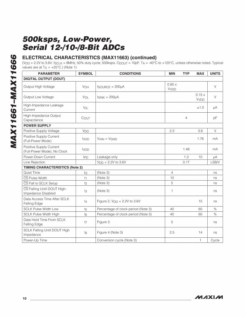
ELECTRICAL CHARACTERISTICS (MAX11663)(VDD = 2.2V to 3.6V. fSCLK = 8MHz, 50% duty cycle, 500ksps. CDOUT = 10pF, TA = -40NC to +125NC, unless otherwise noted. Typical values are at TA = +25NC.) (Note 1)
PARAMETER SYMBOL CONDITIONS MIN TYP MAX UNITS
POWER SUPPLY
Positive Supply Voltage VDD 2.2 3.6 V
Digital I/O Supply Voltage VOVDD 1.5 VDD V
Positive Supply Current (Full-Power Mode)
IVDD VAIN_ = VGND 1.67mA
IOVDD VAIN_ = VGND 0.1
Positive Supply Current (Full-Power Mode), No Clock
IVDD 1.5 mA
Power-Down Current IPD Leakage only 1.3 10 FA
Line Rejection VDD = 2.2V to 3.6V, VREF = 2.2V 0.17 LSB/V
TIMING CHARACTERISTICS (Note 2)
Quiet Time tQ (Note 3) 4 ns
CS Pulse Width t1 (Note 3) 10 ns
CS Fall to SCLK Setup t2 (Note 3) 5 ns
CS Falling Until DOUT High-Impedance Disabled
t3 (Note 3) 1 ns
Data Access Time After SCLK Falling Edge (Figure 2)
t4VOVDD = 2.2V to 3.6V 15
nsVOVDD = 1.5V to 2.2V 16.5
SCLK Pulse Width Low t5 Percentage of clock period (Note 3) 40 60 %
SCLK Pulse Width High t6 Percentage of clock period (Note 3) 40 60 %
Data Hold Time From SCLK Falling Edge
t7 Figure 3 5 ns
SCLK Falling Until DOUT High Impedance
t8 Figure 4 (Note 3) 2.5 14 ns
Power-Up Time Conversion cycle (Note 3) 1 Cycle
PARAMETER SYMBOL CONDITIONS MIN TYP MAX UNITS
DC ACCURACY
Resolution 10 Bits
Integral Nonlinearity INL Q0.5 LSB
Differential Nonlinearity DNL No missing codes Q0.5 LSB
Offset Error OE Q0.3 Q1.3 LSB
Gain Error GE Excluding offset and reference errors Q0.15 Q1.3 LSB
Total Unadjusted Error TUE Q1 LSB

_______________________________________________________________________________________ 9
MA
X1
16
61
–MA
X1
16
66
500ksps, Low-Power, Serial 12-/10-/8-Bit ADCs
ELECTRICAL CHARACTERISTICS (MAX11663) (continued)(VDD = 2.2V to 3.6V. fSCLK = 8MHz, 50% duty cycle, 500ksps. CDOUT = 10pF, TA = -40NC to +125NC, unless otherwise noted. Typical values are at TA = +25NC.) (Note 1)
PARAMETER SYMBOL CONDITIONS MIN TYP MAX UNITS
DYNAMIC PERFORMANCE (fAIN = 250kHz)
Signal-to-Noise and Distortion SINAD 60.5 61.5 dB
Signal-to-Noise Ratio SNR 60.5 61.5 dB
Total Harmonic Distortion THD -85 -73 dB
Spurious-Free Dynamic Range SFDR 75 dB
Intermodulation Distortion IMD f1 = 239.8kHz, f2 = 200.2kHz -82 dB
Full-Power Bandwidth -3dB point 40 MHz
Full-Linear Bandwidth SINAD > 60dB 2.5 MHz
Small-Signal Bandwidth 45 MHz
CONVERSION RATE
Throughput 5 500 ksps
Conversion Time 1.56 Fs
Acquisition Time tACQ 52 ns
Aperture Delay From CS falling edge 4 ns
Aperture Jitter 15 ps
Serial Clock Frequency fCLK 0.08 8 MHz
ANALOG INPUT (AIN)
Input Voltage Range VAIN 0 VDD V
Input Leakage Current IILA 0.002 Q1 FA
Input Capacitance CAINTrack 20
pFHold 4
DIGITAL INPUTS (SCLK, CS, CHSEL)
Digital Input High Voltage VIH0.75 x VVDD
V
Digital Input Low Voltage VIL0.25 x VVDD
V
Digital Input Hysteresis VHYST0.15 x VVDD
V
Digital Input Leakage Current IIL Inputs at GND or VDD 0.001 Q1 FA
Digital Input Capacitance CIN 2 pF
10 _____________________________________________________________________________________
MA
X1
16
61
–MA
X1
16
66
500ksps, Low-Power, Serial 12-/10-/8-Bit ADCsELECTRICAL CHARACTERISTICS (MAX11663) (continued)(VDD = 2.2V to 3.6V. fSCLK = 8MHz, 50% duty cycle, 500ksps. CDOUT = 10pF, TA = -40NC to +125NC, unless otherwise noted. Typical values are at TA = +25NC.) (Note 1)
PARAMETER SYMBOL CONDITIONS MIN TYP MAX UNITS
DIGITAL OUTPUT (DOUT)
Output High Voltage VOH ISOURCE = 200µA0.85 x VVDD
V
Output Low Voltage VOL ISINK = 200µA0.15 x VVDD
V
High-Impedance Leakage Current
IOL Q1.0 FA
High-Impedance Output Capacitance
COUT 4 pF
POWER SUPPLY
Positive Supply Voltage VDD 2.2 3.6 V
Positive Supply Current (Full-Power Mode)
IVDD VAIN = VGND 1.76 mA
Positive Supply Current (Full-Power Mode), No Clock
IVDD 1.48 mA
Power-Down Current IPD Leakage only 1.3 10 FA
Line Rejection VDD = 2.2V to 3.6V 0.17 LSB/V
TIMING CHARACTERISTICS (Note 2)
Quiet Time tQ (Note 3) 4 ns
CS Pulse Width t1 (Note 3) 10 ns
CS Fall to SCLK Setup t2 (Note 3) 5 ns
CS Falling Until DOUT High-Impedance Disabled
t3 (Note 3) 1 ns
Data Access Time After SCLK Falling Edge
t4 Figure 2, VDD = 2.2V to 3.6V 15 ns
SCLK Pulse Width Low t5 Percentage of clock period (Note 3) 40 60 %
SCLK Pulse Width High t6 Percentage of clock period (Note 3) 40 60 %
Data Hold Time From SCLK Falling Edge
t7 Figure 3 5 ns
SCLK Falling Until DOUT High Impedance
t8 Figure 4 (Note 3) 2.5 14 ns
Power-Up Time Conversion cycle (Note 3) 1 Cycle

______________________________________________________________________________________ 11
MA
X1
16
61
–MA
X1
16
66
500ksps, Low-Power, Serial 12-/10-/8-Bit ADCs
ELECTRICAL CHARACTERISTICS (MAX11662)(VDD = 2.2V to 3.6V, VREF = VDD, VOVDD = VDD, fSCLK = 8MHz, 50% duty cycle, 500ksps, CDOUT = 10pF, TA = -40NC to +125NC, unless otherwise noted. Typical values are at TA = +25NC.) (Note 1)
PARAMETER SYMBOL CONDITIONS MIN TYP MAX UNITS
DC ACCURACY
Resolution 8 Bits
Integral Nonlinearity INL Q0.25 LSB
Differential Nonlinearity DNL No missing codes Q0.25 LSB
Offset Error OE 0.45 Q0.8 LSB
Gain Error GE Excluding offset and reference errors 0 Q0.25 LSB
Total Unadjusted Error TUE 0.5 LSB
Channel-to-Channel Offset Matching
0.01 LSB
Channel-to-Channel Gain Matching
0.01 LSB
DYNAMIC PERFORMANCE (fAIN = 250kHz)
Signal-to-Noise and Distortion SINAD 49 49.7 dB
Signal-to-Noise Ratio SNR 49 49.7 dB
Total Harmonic Distortion THD -75 -67 dB
Spurious-Free Dynamic Range SFDR 63 67 dB
Intermodulation Distortion IMD f1 = 239.8kHz, f2 = 200.2kHz -65 dB
Full-Power Bandwidth -3dB point 40 MHz
Full-Linear Bandwidth SINAD > 49dB 2.5 MHz
Small-Signal Bandwidth 45 MHz
Crosstalk -90 dB
CONVERSION RATE
Throughput 5 500 ksps
Conversion Time 1.56 Fs
Acquisition Time tACQ 52 ns
Aperture Delay From CS falling edge 4 ns
Aperture Jitter 15 ps
Serial-Clock Frequency fCLK 0.08 8 MHz
ANALOG INPUT (AIN1, AIN2)
Input Voltage Range VAIN_ 0 VREF V
Input Leakage Current IILA 0.002 Q1 FA
Input Capacitance CAIN_Track 20
pFHold 4
EXTERNAL REFERENCE INPUT (REF)
Reference Input Voltage Range VREF 1VDD + 0.05
V
Reference Input Leakage Current IILR Conversion stopped 0.005 Q1 FA
Reference Input Capacitance CREF 5 pF

12 _____________________________________________________________________________________
MA
X1
16
61
–MA
X1
16
66
500ksps, Low-Power, Serial 12-/10-/8-Bit ADCsELECTRICAL CHARACTERISTICS (MAX11662) (continued)(VDD = 2.2V to 3.6V, VREF = VDD, VOVDD = VDD, fSCLK = 8MHz, 50% duty cycle, 500ksps, CDOUT = 10pF, TA = -40NC to +125NC, unless otherwise noted. Typical values are at TA = +25NC.) (Note 1)
PARAMETER SYMBOL CONDITIONS MIN TYP MAX UNITS
DIGITAL INPUTS (SCLK, CS)
Digital Input High Voltage VIH0.75 x VOVDD
V
Digital Input Low Voltage VIL0.25 x VOVDD
V
Digital Input Hysteresis VHYST0.15 x VOVDD
V
Digital Input Leakage Current IIL Inputs at GND or VDD 0.001 Q1 FA
Digital Input Capacitance CIN 2 pF
DIGITAL OUTPUT (DOUT)
Output High Voltage VOH ISOURCE = 200µA (Note 3)0.85 x VOVDD
V
Output Low Voltage VOL ISINK = 200µA (Note 3)0.15 x VOVDD
V
High-Impedance Leakage Current
IOL Q1.0 FA
High-Impedance Output Capacitance
COUT 4 pF
POWER SUPPLY
Positive Supply Voltage VDD 2.2 3.6 V
Digital I/O Supply Voltage VOVDD 1.5 VDD V
Positive Supply Current (Full-Power Mode)
IVDD VAIN_ = VGND 1.67mA
IOVDD VAIN_ = VGND 0.1Positive Supply Current (Full-Power Mode), No Clock
IVDD 1.5 mA
Power-Down Current IPD Leakage only 1.3 10 FA
Line Rejection VDD = 2.2V to 3.6V, VREF = 2.2V 0.17 LSB/V
TIMING CHARACTERISTICS (Note 2)
Quiet Time tQ (Note 3) 4 ns
CS Pulse Width t1 (Note 3) 10 ns
CS Fall to SCLK Setup t2 (Note 3) 5 ns
CS Falling Until DOUT High-Impedance Disabled
t3 (Note 3) 1 ns
Data Access Time After SCLK Falling Edge (Figure 2)
t4VOVDD = 2.2V to 3.6V (Note 3) 15
nsVOVDD = 1.5V to 2.2V (Note 3) 16.5
SCLK Pulse Width Low t5 Percentage of clock period 40 60 %
SCLK Pulse Width High t6 Percentage of clock period 40 60 %Data Hold Time From SCLK Falling Edge
t7 Figure 3 5 ns
SCLK Falling Until DOUT High Impedance
t8 Figure 4 (Note 3) 2.5 14 ns
Power-Up Time Conversion cycle (Note 3) 1 Cycle
______________________________________________________________________________________ 13
MA
X1
16
61
–MA
X1
16
66
500ksps, Low-Power, Serial 12-/10-/8-Bit ADCs
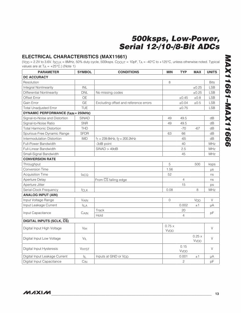
ELECTRICAL CHARACTERISTICS (MAX11661)(VDD = 2.2V to 3.6V. fSCLK = 8MHz, 50% duty cycle, 500ksps. CDOUT = 10pF, TA = -40NC to +125NC, unless otherwise noted. Typical values are at TA = +25NC.) (Note 1)
PARAMETER SYMBOL CONDITIONS MIN TYP MAX UNITS
DC ACCURACY
Resolution 8 Bits
Integral Nonlinearity INL Q0.25 LSB
Differential Nonlinearity DNL No missing codes Q0.25 LSB
Offset Error OE Q0.45 Q0.8 LSB
Gain Error GE Excluding offset and reference errors Q0.04 Q0.5 LSB
Total Unadjusted Error TUE Q0.75 LSB
DYNAMIC PERFORMANCE (fAIN = 250kHz)
Signal-to-Noise and Distortion SINAD 49 49.5 dB
Signal-to-Noise Ratio SNR 49 49.5 dB
Total Harmonic Distortion THD -70 -67 dB
Spurious-Free Dynamic Range SFDR 63 66 dB
Intermodulation Distortion IMD f1 = 239.8kHz, f2 = 200.2kHz -65 dB
Full-Power Bandwidth -3dB point 40 MHz
Full-Linear Bandwidth SINAD > 49dB 2.5 MHz
Small-Signal Bandwidth 45 MHz
CONVERSION RATE
Throughput 5 500 ksps
Conversion Time 1.56 Fs
Acquisition Time tACQ 52 ns
Aperture Delay From CS falling edge 4 ns
Aperture Jitter 15 ps
Serial-Clock Frequency fCLK 0.08 8 MHz
ANALOG INPUT (AIN)
Input Voltage Range VAIN 0 VDD V
Input Leakage Current IILA 0.002 Q1 FA
Input Capacitance CAINTrack 20
pFHold 4
DIGITAL INPUTS (SCLK, CS)
Digital Input High Voltage VIH0.75 x VVDD
V
Digital Input Low Voltage VIL0.25 x VVDD
V
Digital Input Hysteresis VHYST0.15 VVDD
V
Digital Input Leakage Current IIL Inputs at GND or VDD 0.001 Q1 FA
Digital Input Capacitance CIN 2 pF
14 _____________________________________________________________________________________
MA
X1
16
61
–MA
X1
16
66
500ksps, Low-Power, Serial 12-/10-/8-Bit ADCsELECTRICAL CHARACTERISTICS (MAX11661) (continued)(VDD = 2.2V to 3.6V. fSCLK = 8MHz, 50% duty cycle, 500ksps. CDOUT = 10pF, TA = -40NC to +125NC, unless otherwise noted. Typical values are at TA = +25NC.) (Note 1)
Note 1: Limits at TA = -40NC are guaranteed by design and not production tested. Note 2: All timing specifications given are with a 10pF capacitor.Note 3: Guaranteed by design in characterization; not production tested.
PARAMETER SYMBOL CONDITIONS MIN TYP MAX UNITS
DIGITAL OUTPUT (DOUT)
Output High Voltage VOH ISOURCE = 200µA0.85 x VVDD
V
Output Low Voltage VOL ISINK = 200µA0.15 x VVDD
V
High-Impedance Leakage Current
IOL Q1.0 FA
High-Impedance Output Capacitance
COUT 4 pF
POWER SUPPLY
Positive Supply Voltage VDD 2.2 3.6 V
Positive Supply Current (Full-Power Mode)
IVDD VAIN = VGND 1.76 mA
Positive Supply Current (Full-Power Mode), No Clock
IVDD 1.48 mA
Power-Down Current IPD Leakage only 1.3 10 FA
Line Rejection VDD = 2.2V to 3.6V 0.17 LSB/V
TIMING CHARACTERISTICS (Note 2)
Quiet Time tQ (Note 3) 4 ns
CS Pulse Width t1 (Note 3) 10 ns
CS Fall to SCLK Setup t2 (Note 3) 5 ns
CS Falling Until DOUT High-Impedance Disabled
t3 (Note 3) 1 ns
Data Access Time After SCLK Falling Edge
t4 Figure 2, VDD = 2.2V to 3.6V 15 ns
SCLK Pulse Width Low t5 Percentage of clock period (Note 3) 40 60 %
SCLK Pulse Width High t6 Percentage of clock period (Note 3) 40 60 %
Data Hold Time From SCLK Falling Edge
t7 Figure 3 5 ns
SCLK Falling Until DOUT High Impedance
t8 Figure 4 (Note 3) 2.5 14 ns
Power-Up Time Conversion cycle (Note 3) 1 Cycle

______________________________________________________________________________________ 15
MA
X1
16
61
–MA
X1
16
66
500ksps, Low-Power, Serial 12-/10-/8-Bit ADCs
Figure 1. Interface Signals for Maximum Throughput, 12-Bit Devices
Figure 2. Setup Time After SCLK Falling Edge Figure 3. Hold Time After SCLK Falling Edge
Figure 4. SCLK Falling Edge DOUT Three-State
1 2 3 4 5 6 7 8 9 10 11 12 13 14 15 1616 1
D11 D10 D9 D8 D7 D6 D5 D4 D3 D2 D1 D0DOUT
SCLK
HIGHIMPEDANCE
t6
t2
t5
t1
0
SAMPLE SAMPLE
0 0
(MSB)
t3 t4 t7 t8 tQUIET
tCONVERT
1/fSAMPLE
tACQ
CS
HIGHIMPEDANCE
VIH
VILNEW DATAOLD DATADOUT
SCLK
t4
VIH
VIL
OLD DATA NEW DATADOUT
SCLK
t7
HIGH IMPEDANCEDOUT
SCLK
t8

16 _____________________________________________________________________________________
MA
X1
16
61
–MA
X1
16
66
500ksps, Low-Power, Serial 12-/10-/8-Bit ADCs Typical Operating Characteristics(MAX11665AUT+, TA = +25°C, unless otherwise noted.)
SOT23 TYPICAL OPERATING CHARACTERISTICSDIFFERENTIAL NONLINEARITY (DNL)
vs. OUTPUT CODE
MAX
1166
1 to
c02
DIGITAL OUTPUT CODE (DECIMAL)
DNL
(LSB
)
300020001000
-0.5
0
0.5
1.0
-1.00 4000
OFFSET ERROR vs. TEMPERATURE
MAX
1166
1 to
c03
TEMPERATURE (°C)
OFFS
ET E
RROR
(LSB
)
1109580655035205-10-25
1
2
3
0-40 125
INTEGRAL NONLINEARITY (INL) vs. OUTPUT CODE
MAX
1166
1 to
c01
DIGITAL OUTPUT CODE (DECIMAL)
INL
(LSB
)
300020001000
-0.5
0
0.5
1.0
-1.00 4000
THD vs. ANALOG INPUT FREQUENCY
MAX
1166
1 to
c06
fIN (kHz)
THD
(dB)
20015010050
-90
-80
-70
-1000 250
GAIN ERROR vs. TEMPERATURE
MAX
1166
1 to
c04
TEMPERATURE (°C)
GAIN
ERR
OR (L
SB)
1109580655035205-10-25
-1
0
1
2
-2-40 125
SPURIOUS-FREE DYNAMIC RANGE (SFDR) vs. ANALOG INPUT FREQUENCY
MAX
1166
1 to
c07
fIN (kHz)
SFDR
(dB)
20015010050
87
89
91
93
95
850 250
SIGNAL-TO-NOISE RATIO (SNR) vs. ANALOG INPUT FREQUENCY
MAX
1166
1 to
c05
fIN (kHz)
SNR
(dB)
20015010050
72
74
76
700 250

______________________________________________________________________________________ 17
MA
X1
16
61
–MA
X1
16
66
500ksps, Low-Power, Serial 12-/10-/8-Bit ADCs
Typical Operating Characteristics (continued)(MAX11665AUT+, TA = +25°C, unless otherwise noted.)
SOT23 TYPICAL OPERATING CHARACTERISTICS
SUPPLY CURRENT vs. TEMPERATURE
MAX
1166
1 to
c10
TEMPERATURE (°C)
I VDD
(mA)
1109580655035205-10-25
1.3
1.4
1.5
1.6
VDD = 3.6V
VDD = 3V
VDD = 2.2V
1.2-40 125
SIGNAL-TO-NOISE AND DISTORTION RATIO(SINAD) vs. ANALOG INPUT FREQUENCY
MAX
1166
1 to
c08
fIN (kHz)
SINA
D (d
B)
20015010050
72
74
76
700 250
HISTOGRAM FOR 30,000 CONVERSIONS
MAX
1166
1 to
c12
DIGITAL CODE OUTPUT
CODE
COU
NT
2050204920482047
5000
10,000
15,000
20,000
25,000
30,000
35,000
02046
SIGNAL-TO-NOISE RATIO (SNR) vs. SUPPLY VOLTAGE (VDD)
MAX
1166
1 to
c11
VDD (V)
SNR
(dB)
3.43.23.02.82.62.4
72
73
74
75
712.2 3.6
FREQUENCY (kHz)
MAG
NITU
DE (d
B)
20015010050
-100
-80
-60
-40
AHD2 = - 88dB
-20
0
-1200 250
100kHz SINE-WAVE INPUT
MAX
1166
1 to
c09
fIN = 99.4kHzfS = 500kspsVDD = 3V
THD vs. INPUT RESISTANCE
MAX
1166
1 to
c13
RIN (I)
THD
(dB)
80604020
-95
-90
-85
-80
-75fS = 500kspsfIN = 250kHz
-1000 100

18 _____________________________________________________________________________________
MA
X1
16
61
–MA
X1
16
66
500ksps, Low-Power, Serial 12-/10-/8-Bit ADCs
Pin Description
Pin Configurations
*CONNECT EP TO GROUND PLANE. DEVICES DO NOT OPERATE WHEN EP IS NOT CONNECTED TO GROUND!
EP*
TOP VIEW
+
TOP VIEW
GND
SCLKAIN
1 6 CS
5 DOUT
VDD
MAX11661MAX11663MAX11665
SOT23
2
3 4
+
µMAX
2 9 DOUTAIN2
1 10 SCLKAIN1
OVDDAGND 3 8
CHSELREF 7
CSVDD 6
MAX11662MAX11664MAX116664
5
PINNAME FUNCTION
µMAX SOT23
1 — AIN1Analog Input Channel 1. Single-ended analog input with respect to AGND with range of 0V to VREF.
2 — AIN2Analog Input Channel 2. Single-ended analog input with respect to AGND with range of 0V to VREF.
— 3 AIN Analog Input Channel. Single-ended analog input with respect to GND with range of 0V to VDD.
— 2 GND Ground. Connect GND to the GND ground plane.
3 — AGND Analog Ground. Connect AGND directly the GND ground plane.
4 — REFExternal Reference Input. REF defines the signal range of the input signal AIN1/AIN2: 0V to VREF. The range of VREF is 1V to VDD. Bypass REF to AGND with 10FF || 0.1FF capacitor.
5 1 VDD
Positive Supply Voltage. Bypass VDD with a 10FF || 0.1FF capacitor to GND. VDD range is 2.2V to 3.6V. For the SOT23 package, VDD also defines the signal range of the input signal AIN: 0V to VDD.
6 6 CSActive-Low Chip-Select Input. The falling edge of CS samples the analog input signal, starts a conversion, and frames the serial-data transfer.
7 — CHSELChannel Select. Set CHSEL high to select AIN2 for conversion. Set CHSEL low to select AIN1 for conversion.
8 — OVDD Digital Interface Supply for SCLK, CS, DOUT, and CHSEL. The OVDD range is 1.5V to VDD. Bypass OVDD with a 10FF || 0.1FF capacitor to GND.
9 5 DOUTThree-State Serial-Data Output. ADC conversion results are clocked out on the falling edge of SCLK, MSB first. See Figure 1.
10 4 SCLKSerial-Clock Input. SCLK drives the conversion process. DOUT is updated on the falling edge of SCLK. See Figures 2 and 3.
— — EPExposed Pad (µMAX Only). Connect EP directly to a solid ground plane. Devices do not operate when EP is not connected to ground!

______________________________________________________________________________________ 19
MA
X1
16
61
–MA
X1
16
66
500ksps, Low-Power, Serial 12-/10-/8-Bit ADCs
Functional Diagrams
Typical Operating Circuit
CDACMUX
REF
AIN2
AIN1
CHSEL
CONTROLLOGIC
SAROUTPUTBUFFER
SCLK
CS
VDD OVDD
DOUT
MAX11662MAX11664MAX11666
CDACAIN
CONTROLLOGIC
SAROUTPUTBUFFER
SCLK
CS
DOUT
VDD
GND
VREF = VDD
MAX11661MAX11663MAX11665
GND (EP)AGND
VDD OVDD
SCLK
CPU
DOUT
CS
CHSEL
AIN1SCK
MISO
AIN2
AGND
REF
+3V VOVDD
ANALOGINPUTS
+2.5V
SS
VDD
CPU
AIN
GND
+3V
ANALOGINPUT
DOUT MISO
SCLK SCK
CS SS
GND (EP)
MAX11662MAX11664MAX11666
MAX11661MAX11663MAX11665

20 _____________________________________________________________________________________
MA
X1
16
61
–MA
X1
16
66
500ksps, Low-Power, Serial 12-/10-/8-Bit ADCs Detailed DescriptionThe MAX11661–MAX11666 are fast, 12-/10-/8-bit, low-power, single-supply ADCs. The devices operate from a 2.2V to 3.6V supply and consume only 2.98mW (VDD = 2.2V) or 4.37mW (VDD = 3V). These devices are capable of sampling at full rate when driven by an 8MHz clock. The dual-channel devices provide a separate digital supply input (OVDD) to power the digi-tal interface enabling communication with 1.5V, 1.8V, 2.5V, or 3V digital systems.
The conversion result appears at DOUT, MSB first, with a leading zero followed by the 12-bit, 10-bit, or 8-bit result. A 12-bit result is followed by two trailing zeros, a 10-bit result is followed by four trailing zeros, and an 8-bit result is followed by six trailing zeros. See Figures 1 and 5.
The dual-channel devices feature a dedicated refer-ence input (REF). The input signal range for AIN1/AIN2 is defined as 0V to VREF with respect to AGND. The single-channel devices use VDD as the reference. The input signal range of AIN is defined as 0V to VDD with respect to GND.
These ADCs include a power-down feature allowing minimized power consumption at 2.5FA/ksps for lower
throughput rates. The wake-up and power-down feature is controlled by using the SPI interface as described in the Operating Modes section.
Serial InterfaceThe devices feature a 3-wire serial interface that directly connects to SPI, QSPI, and MICROWIRE devices without external logic. Figures 1 and 5 show the interface sig-nals for a single conversion frame to achieve maximum throughput.
The falling edge of CS defines the sampling instant. Once CS transitions low, the external clock signal (SCLK) controls the conversion.
The SAR core successively extracts binary-weighted bits in every clock cycle. The MSB appears on the data bus during the 2nd clock cycle with a delay outlined in the timing specifications. All extracted data bits appear suc-cessively on the data bus with the LSB appearing during the 13th/11th/9th clock cycle for 12-/10-/8-bit operation. The serial data stream of conversion bits is preceded by a leading “zero” and succeeded by trailing “zeros.” The data output (DOUT) goes into a high-impedance state during the 16th clock cycle.
Figure 5. 10-/8-Bit Timing Diagrams
SCLK 1 2 3 4 5 6 7 8 9 10 11 12 13 14 15 1616 1
SAMPLE SAMPLE
CS
DOUT
HIGHIMPEDANCE
HIGHIMPEDANCE
HIGHIMPEDANCE
HIGHIMPEDANCE
0 0 0D9 D8 D7 D6 D5 D4 D3 D2 D1 D0 0 0
SAMPLE SAMPLE
SCLK
CS
1 2 3 4 5 6 7 8 9 10 11 12 13 14 15 1616 1
DOUT 0 0 0D7 D6 D5 D4 D3 D2 D1 D0 0 00 0

______________________________________________________________________________________ 21
MA
X1
16
61
–MA
X1
16
66
500ksps, Low-Power, Serial 12-/10-/8-Bit ADCs
To sustain the maximum sample rate, all devices have to be resampled immediately after the 16th clock cycle. For lower sample rates, the CS falling edge can be delayed leaving DOUT in a high-impedance condition. Pull CS high after the 10th SCLK falling edge (see the Operating Modes section).
Analog InputThe devices produce a digital output that corresponds to the analog input voltage within the specified operating range of 0V to VREF for the dual-channel devices and 0V to VDD for the single-channel devices.
Figure 6 shows an equivalent circuit for the analog input AIN (for single-channel devices) and AIN1/AIN2 (for dual-channel devices). Internal protection diodes D1/D2 confine the analog input voltage within the power rails (VDD, GND). The analog input voltage can swing from GND - 0.3V to VDD + 0.3V without damaging the device.
The electric load presented to the external stage driv-ing the analog input varies depending on which mode the ADC is in: track mode vs. conversion mode. In track mode, the internal sampling capacitor CS (16pF) has to be charged through the resistor R (R = 50I) to the input voltage. For faithful sampling of the input, the capacitor voltage on CS has to settle to the required accuracy dur-ing the track time.
The source impedance of the external driving stage in conjunction with the sampling switch resistance affects the settling performance. The THD vs. Input Resistance graph in the Typical Operating Characteristics shows THD sensitivity as a function of the signal source imped-ance. Keep the source impedance at a minimum for high-dynamic-performance applications. Use a high-performance op amp such as the MAX4430 to drive the analog input, thereby decoupling the signal source and the ADC.
While the ADC is in conversion mode, the sampling switch is open presenting a pin capacitance, CP (CP = 5pF), to the driving stage. See the Applications Information section for information on choosing an appropriate buffer for the ADC.
ADC Transfer FunctionThe output format is straight binary. The code transi-tions midway between successive integer LSB values such as 0.5 LSB, 1.5 LSB, etc. The LSB size for single-channel devices is VDD/2n and for dual-channel devices is VREF/2n, where n is the resolution. The ideal transfer characteristic is shown in Figure 10.
Operating ModesThe ICs offer two modes of operation: normal mode and power-down mode. The logic state of the CS signal during a conversion activates these modes. The power-down mode can be used to optimize power dissipation with respect to sample rate.
Normal ModeIn normal mode, the devices are powered up at all times, thereby achieving their maximum throughput rates. Figure 7 shows the timing diagram of these devices in normal mode. The falling edge of CS samples the analog input signal, starts a conversion, and frames the serial-data transfer.
Figure 6. Analog Input Circuit
Figure 7. Normal Mode
CP
AIN1/AIN2
VDD
AIN
D2
D1R
CS
SWITCH CLOSED IN TRACK MODESWITCH OPEN IN CONVERSION MODE
1 2 3 4 5 6 7 8 9 10 11 12 13 14 15 16SCLK
PULL CS HIGH AFTER THE 10TH SCLK FALLING EDGEKEEP CS LOW UNTIL AFTER THE 10TH SCLK FALLING EDGE
CS
DOUT VALID DATAHIGH
IMPEDANCEHIGH
IMPEDANCE

22 _____________________________________________________________________________________
MA
X1
16
61
–MA
X1
16
66
500ksps, Low-Power, Serial 12-/10-/8-Bit ADCs
To remain in normal mode, keep CS low until the falling edge of the 10th SCLK cycle. Pulling CS high after the 10th SCLK falling edge keeps the part in normal mode.
However, pulling CS high before the 10th SCLK falling edge terminates the conversion, DOUT goes into high-impedance mode, and the device enters power-down mode. See Figure 8.
Power-Down Mode In power-down mode, all bias circuitry is shut down drawing typically only 1.3FA of leakage current. To save power, put the device in power-down mode between conversions. Using the power-down mode between conversions is ideal for saving power when sampling the analog input infrequently.
Entering Power-Down ModeTo enter power-down mode, drive CS high between the 2nd and 10th falling edges of SCLK (see Figure 8). By pulling CS high, the current conversion terminates and DOUT enters high impedance.
Exiting Power-Down ModeTo exit power-down mode, implement one dummy con-version by driving CS low for at least 10 clock cycles (see Figure 9). The data on DOUT is invalid during this dummy conversion. The first conversion following the dummy cycle contains a valid conversion result.
The power-up time equals the duration of the dummy cycle, and is dependent on the clock frequency. The power-up time for 500ksps operation (8MHz SCLK) is 2Fs.
Figure 8. Entering Power-Down Mode
Figure 9. Exiting Power-Down Mode
Figure 10. ADC Transfer Function
1 2 3 4 5 6 7 8 9 10 11 12 13 14 15 16
HIGHIMPEDANCE INVALID
DATA
SCLK
CS
DOUT
INVALID DATA OR HIGH IMPEDANCE HIGH IMPEDANCE
PULL CS HIGH AFTER THE 2ND AND BEFORE THE 10TH SCLK FALLING EDGE
1 2 3 4 5 6 7 8 9 10 11 12 13 14 15 16 N 1 2 3 4 5 6 7 8 9 10 11 12 13 14 15 16
HIGHIMPEDANCE
HIGHIMPEDANCE
HIGHIMPEDANCE
SCLK
CS
DOUT INVALID DATA (DUMMY CONVERSION) VALID DATA
FS - 1.5 x LSBOUTPUT CODE
ANALOGINPUT (LSB)
111...111
111...110
111...101
0 1 2 3 2n-2 2n-1 2n000...000
000...001
000...010
FULL SCALE (FS):AIN1/AIN2 = REF (TDFN, µMAX)
AIN = VDD (SOT23)n = RESOLUTION

______________________________________________________________________________________ 23
MA
X1
16
61
–MA
X1
16
66
500ksps, Low-Power, Serial 12-/10-/8-Bit ADCs
Supply Current vs. Sampling Rate For applications requiring lower throughput rates, the user can reduce the clock frequency (fSCLK) to lower the sample rate. Figure 11 shows the typical supply current (IVDD) as a function of sample rate (fS) for the 500ksps devices. The part operates in normal mode and
is never powered down. The user can also power down the ADC between conversions by using the power-down mode. Figure 12 shows for the 500ksps device that as the sample rate is reduced, the device remains in the power-down state longer and the average supply cur-rent (IVDD) drops accordingly.
Figure 11. Supply Current vs. Sample Rate (Normal Operating Mode)
Figure 12. Supply Current vs. Sample Rate (Device Powered Down Between Conversions)
SUPPLY CURRENT vs. SAMPLING RATE
SAMPLING RATE (ksps)
I VDD
(mA)
400300200100
0.5
1.0
1.5
2.0VDD = 3VfSCLK = VARIABLE16 CYCLES/CONVERSIONS
00 500
SUPPLY CURRENT vs. SAMPLING RATE
SAMPLING RATE (ksps)
I VDD
(mA)
14012010080604020
0.5
1.0
1.5VDD = 3VfSCLK = 8MHz
00 160

24 _____________________________________________________________________________________
MA
X1
16
61
–MA
X1
16
66
500ksps, Low-Power, Serial 12-/10-/8-Bit ADCs
Figure 13. Channel Select Timing Diagram
Dual-Channel OperationThe MAX11662/MAX11664/MAX11666 feature dual-input channels. These devices use a channel-select (CHSEL) input to select between analog input AIN1 (CHSEL = 0) or AIN2 (CHSEL = 1). As shown in Figure 13, the CHSEL signal is required to change between the 2nd and 12th clock cycle within a regular conversion to guarantee proper switching between channels.
14-Cycle Conversion ModeThe ICs can operate with 14 cycles per conversion. Figure 14 shows the corresponding timing diagram. Observe that DOUT does not go into high-impedance mode. Also, observe that tACQ needs to be sufficiently long to guarantee proper settling of the analog input voltage. See the Electrical Characteristics table for tACQ requirements and the Analog Input section for a descrip-tion of the analog inputs.
Applications InformationLayout, Grounding, and Bypassing
For best performance, use PCBs with a solid ground plane. Ensure that digital and analog signal lines are separated from each other. Do not run analog and digital (especially clock) lines parallel to one another or digital lines underneath the ADC package. Noise in the VDD power supply, OVDD, and REF affects the ADC’s perfor-mance. Bypass the VDD, OVDD, and REF to ground with 0.1FF and 10FF bypass capacitors. Minimize capacitor lead and trace lengths for best supply-noise rejection.
Choosing an Input AmplifierIt is important to match the settling time of the input amplifier to the acquisition time of the ADC. The conver-sion results are accurate when the ADC samples the input signal for an interval longer than the input signal’s worst-case settling time. By definition, settling time is the interval between the application of an input voltage step and the point at which the output signal reaches
Figure 14. 14-Clock Cycle Operation
1
DATA CHANNEL AIN1 DATA CHANNEL AIN2
SCLK
CHSEL
DOUT
CS
2 3 4 5 6 7 8 9 10 11 12 13 14 15 16 1 2 3 4 5 6 7 8 9 10 11 12 13 14 15 16
1
DOUT
SCLK
(MSB)
SAMPLE SAMPLE
1/fSAMPLE
tACQ
tCONVERT
CS
2 3 4
D10D11
5 6 7 8 9 10 11 12 13 14 1
D9 D8 D7 D6 D5 D4 D3 D2 D1 D0 0 00

______________________________________________________________________________________ 25
MA
X1
16
61
–MA
X1
16
66
500ksps, Low-Power, Serial 12-/10-/8-Bit ADCs
and stays within a given error band centered on the resulting steady-state amplifier output level. The ADC input sampling capacitor charges during the sampling cycle, referred to as the acquisition period. During this acquisition period, the settling time is affected by the input resistance and the input sampling capacitance. This error can be estimated by looking at the settling of an RC time constant using the input capacitance and the source impedance over the acquisition time period.
Figure 15 shows a typical application circuit. The MAX4430, offering a settling time of 37ns at 16 bits, is an excellent choice for this application. See the THD vs. Input Resistance graph in the Typical Operating Characteristics.
Choosing a ReferenceFor devices using an external reference, the choice of the reference determines the output accuracy of the ADC. An ideal voltage reference provides a perfect initial accuracy and maintains the reference voltage indepen-dent of changes in load current, temperature, and time. Considerations in selecting a reference include initial voltage accuracy, temperature drift, current source, sink capability, quiescent current, and noise. Figure 15 shows a typical application circuit using the MAX6126 to provide the reference voltage. The MAX6033 and MAX6043 are also excellent choices.
Figure 15. Typical Application Circuit
MAX11662MAX11664MAX11666
MAX6126
OVDD
VOVDD3V
SCLK
CPU
DOUT
CHSEL
SCK
MISO
CS SS
0.1µF
1µF
10µF
0.1µF
AGND
AIN1
AIN1
VDC
4
1
5
2
2
3
AIN2
VDD
7 2
1
6
4
3
10µF
0.1µF
0.1µF
0.1µF
+5V
-5V 470pFC0G CAPACITOR
10I
500I
470pFC0G CAPACITOR
10µF
+5V
10µF
0.1µF
0.1µF 10µF
REF
OUTF IN
NR
OUTS
GNDS
GND
EP
MAX4430
AIN2
VDC
4
1
5
3
0.1µF
+5V
-5V
10I
10µF
0.1µF 10µF
MAX4430
500I
500I
500I
100pF C0G
100pF C0G

26 _____________________________________________________________________________________
MA
X1
16
61
–MA
X1
16
66
500ksps, Low-Power, Serial 12-/10-/8-Bit ADCs Definitions
Integral NonlinearityIntegral nonlinearity (INL) is the deviation of the values on an actual transfer function from a straight line. For these devices, the straight line is a line drawn between the end points of the transfer function after offset and gain errors are nulled.
Differential NonlinearityDifferential nonlinearity (DNL) is the difference between an actual step width and the ideal value of 1 LSB. A DNL error specification of ±1 LSB or less guarantees no mis-sing codes and a monotonic transfer function.
Offset Error The deviation of the first code transition (00 . . . 000) to (00 . . . 001) from the ideal, that is, AGND + 0.5 LSB.
Gain Error The deviation of the last code transition (111 . . . 110) to (111 . . . 111) from the ideal after adjusting for the offset error, that is, VREF - 1.5 LSB.
Aperture JitterAperture jitter (tAJ) is the sample-to-sample variation in the time between the samples.
Aperture DelayAperture delay (tAD) is the time between the falling edge of sampling clock and the instant when an actual sample is taken.
Signal-to-Noise Ratio (SNR)SNR is a dynamic figure of merit that indicates the con-verter’s noise performance. For a waveform perfectly reconstructed from digital samples, the theoretical maxi-mum SNR is the ratio of the full-scale analog input (RMS value) to the RMS quantization error (residual error). The ideal, theoretical minimum analog-to-digital noise is caused by quantization error only and results directly from the ADC’s resolution (N bits):
SNR (dB) (MAX) = (6.02 x N + 1.76) (dB)
In reality, there are other noise sources such as thermal noise, reference noise, and clock jitter that also degrade SNR. SNR is computed by taking the ratio of the RMS signal to the RMS noise. RMS noise includes all spectral components to the Nyquist frequency excluding the fundamental, the first five harmonics, and the DC offset.
Signal-to-Noise Ratio and Distortion (SINAD)
SINAD is a dynamic figure of merit that indicates the converter’s noise and distortion performance. SINAD is computed by taking the ratio of the RMS signal to the RMS noise plus distortion. RMS noise plus distor-tion includes all spectral components to the Nyquist frequency excluding the fundamental and the DC offset:
.
( )RMS
RMS
SIGNALSINAD(dB) 20 log
NOISE DISTORTION
= ×
+
Total Harmonic DistortionTotal harmonic distortion (THD) is the ratio of the RMS sum of the first five harmonics of the input signal to the fundamental itself. This is expressed as:
2 2 2 22 3 4 5
1
V V V VTHD 20 log
V
+ + + = ×
where V1 is the fundamental amplitude and V2–V5 are the amplitudes of the 2nd- through 5th-order harmonics.
Spurious-Free Dynamic Range (SFDR)SFDR is a dynamic figure of merit that indicates the low-est usable input signal amplitude. SFDR is the ratio of the RMS amplitude of the fundamental (maximum signal component) to the RMS value of the next largest spuri-ous component, excluding DC offset. SFDR is specified in decibels with respect to the carrier (dBc).
Full-Power BandwidthFull-power bandwidth is the frequency at which the input signal amplitude attenuates by 3dB for a full-scale input.
Full-Linear BandwidthFull-linear bandwidth is the frequency at which the signal-to-noise ratio and distortion (SINAD) is equal to a specified value.
Intermodulation DistortionAny device with nonlinearities creates distortion prod-ucts when two sine waves at two different frequencies (f1 and f2) are applied into the device. Intermodulation distortion (IMD) is the total power of the IM2 to IM5 inter-modulation products to the Nyquist frequency relative to the total input power of the two input tones, f1 and f2. The individual input tone levels are at -6dBFS.
______________________________________________________________________________________ 27
MA
X1
16
61
–MA
X1
16
66
500ksps, Low-Power, Serial 12-/10-/8-Bit ADCs
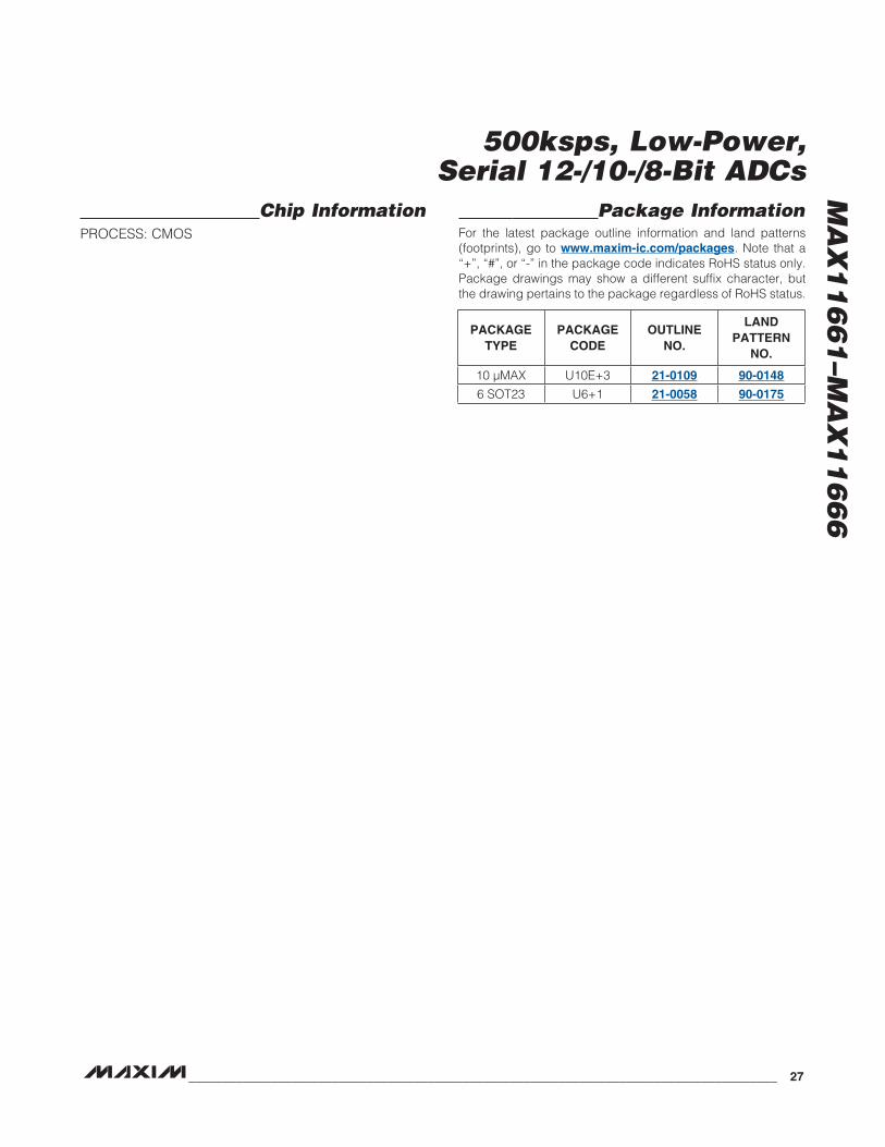
Chip InformationPROCESS: CMOS
Package InformationFor the latest package outline information and land patterns (footprints), go to www.maxim-ic.com/packages. Note that a “+”, “#”, or “-” in the package code indicates RoHS status only. Package drawings may show a different suffix character, but the drawing pertains to the package regardless of RoHS status.
PACKAGE TYPE
PACKAGE CODE
OUTLINE NO.
LAND PATTERN
NO.
10 µMAX U10E+3 21-0109 90-0148
6 SOT23 U6+1 21-0058 90-0175
Maxim cannot assume responsibility for use of any circuitry other than circuitry entirely embodied in a Maxim product. No circuit patent licenses are implied. Maxim reserves the right to change the circuitry and specifications without notice at any time. The parametric values (min and max limits) shown in the Electrical Characteristics table are guaranteed. Other parametric values quoted in this data sheet are provided for guidance.
28 Maxim Integrated Products, 120 San Gabriel Drive, Sunnyvale, CA 94086 408-737-7600© 2012 Maxim Integrated Products Maxim is a registered trademark of Maxim Integrated Products, Inc.
MA
X1
16
61
–MA
X1
16
66
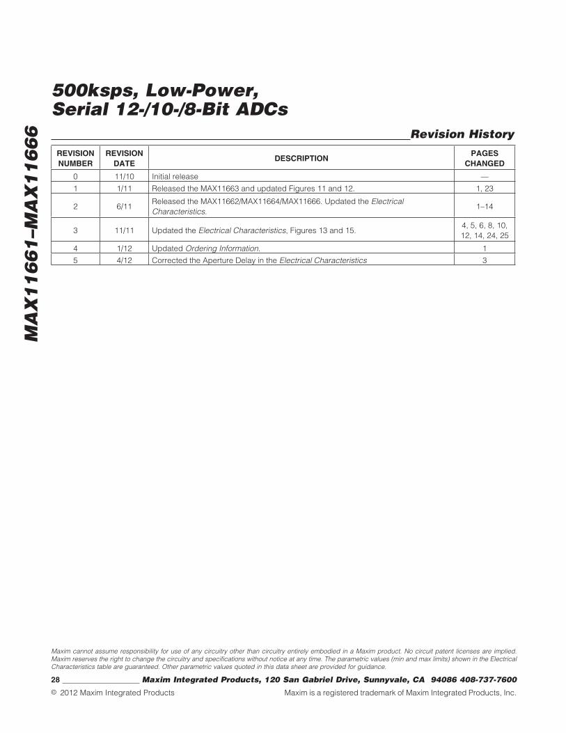
500ksps, Low-Power, Serial 12-/10-/8-Bit ADCs Revision History
REVISIONNUMBER
REVISIONDATE
DESCRIPTIONPAGES
CHANGED
0 11/10 Initial release —
1 1/11 Released the MAX11663 and updated Figures 11 and 12. 1, 23
2 6/11Released the MAX11662/MAX11664/MAX11666. Updated the Electrical Characteristics.
1–14
3 11/11 Updated the Electrical Characteristics, Figures 13 and 15.4, 5, 6, 8, 10, 12, 14, 24, 25
4 1/12 Updated Ordering Information. 1
5 4/12 Corrected the Aperture Delay in the Electrical Characteristics 3