
A ROUTER FOR MASSIVELY-PARALLEL NEURAL...
165
A ROUTER FOR MASSIVELY-PARALLEL NEURAL SIMULATION A thesis submitted to the University of Manchester for the degree of Doctor of Philosophy in the Faculty of Engineering and Physical Sciences 2010 By Jian Wu School of Computer Science
Transcript of A ROUTER FOR MASSIVELY-PARALLEL NEURAL...
A ROUTER FOR
MASSIVELY-PARALLEL
NEURAL SIMULATION
A thesis submitted to the University of Manchester
for the degree of Doctor of Philosophy
in the Faculty of Engineering and Physical Sciences
2010
By
Jian Wu
School of Computer Science
Contents
Abstract 11
Declaration 12
Copyright 13
Acknowledgements 14
1 Introduction 15
1.1 Neural simulation . . . . . . . . . . . . . . . . . . . . . . . . . . . 17
1.2 Literature review . . . . . . . . . . . . . . . . . . . . . . . . . . . 17
1.2.1 Software neural simulators . . . . . . . . . . . . . . . . . . 18
1.2.2 Neural simulations on general-purpose computers . . . . . 18
1.2.3 Neurocomputers . . . . . . . . . . . . . . . . . . . . . . . . 19
1.2.4 Limitations of previous neural simulators . . . . . . . . . . 21
1.3 Design considerations . . . . . . . . . . . . . . . . . . . . . . . . . 23
1.4 Contributions . . . . . . . . . . . . . . . . . . . . . . . . . . . . . 24
1.5 Dissertation organization . . . . . . . . . . . . . . . . . . . . . . . 25
1.6 Publications . . . . . . . . . . . . . . . . . . . . . . . . . . . . . . 25
2 Neurcomputing 28
2.1 Introduction . . . . . . . . . . . . . . . . . . . . . . . . . . . . . . 28
2.2 Biological neurons and neural networks . . . . . . . . . . . . . . . 30
2.3 Mathematical neurobiology . . . . . . . . . . . . . . . . . . . . . . 32
2.3.1 Artificial neuron . . . . . . . . . . . . . . . . . . . . . . . 32
2.3.2 Artificial neural networks . . . . . . . . . . . . . . . . . . . 33
2.4 Spiking neural network . . . . . . . . . . . . . . . . . . . . . . . . 35
2.4.1 Generations of spiking neural models . . . . . . . . . . . . 36
2
2.4.2 Izhikevich model . . . . . . . . . . . . . . . . . . . . . . . 36
2.5 Summary . . . . . . . . . . . . . . . . . . . . . . . . . . . . . . . 37
3 Networks-on-Chip 39
3.1 Introduction . . . . . . . . . . . . . . . . . . . . . . . . . . . . . . 39
3.2 Benefits of adopting NoCs . . . . . . . . . . . . . . . . . . . . . . 41
3.3 NoC topologies . . . . . . . . . . . . . . . . . . . . . . . . . . . . 42
3.4 Router architecture and switching schemes . . . . . . . . . . . . . 45
3.4.1 Router architecture . . . . . . . . . . . . . . . . . . . . . . 46
3.4.2 Switching schemes . . . . . . . . . . . . . . . . . . . . . . 46
3.5 Routing algorithms . . . . . . . . . . . . . . . . . . . . . . . . . . 48
3.5.1 Source routing and distributed routing . . . . . . . . . . . 48
3.5.2 Deterministic routing and adaptive routing . . . . . . . . . 49
3.6 Deadlock and livelock avoidance . . . . . . . . . . . . . . . . . . . 50
3.7 Summary . . . . . . . . . . . . . . . . . . . . . . . . . . . . . . . 51
4 A NoC-based neurocomputing platform 52
4.1 Introduction . . . . . . . . . . . . . . . . . . . . . . . . . . . . . . 52
4.2 Design issues . . . . . . . . . . . . . . . . . . . . . . . . . . . . . 54
4.3 Overview of SpiNNaker . . . . . . . . . . . . . . . . . . . . . . . . 56
4.3.1 Multicasting . . . . . . . . . . . . . . . . . . . . . . . . . . 57
4.3.2 Processing node . . . . . . . . . . . . . . . . . . . . . . . . 60
4.3.3 Fault-tolerance . . . . . . . . . . . . . . . . . . . . . . . . 62
4.4 Event-driven communication . . . . . . . . . . . . . . . . . . . . . 62
4.4.1 Address event representation . . . . . . . . . . . . . . . . . 63
4.4.2 AER communication based on a router . . . . . . . . . . . 64
4.5 Communication NoC . . . . . . . . . . . . . . . . . . . . . . . . . 65
4.6 System NoC . . . . . . . . . . . . . . . . . . . . . . . . . . . . . . 66
4.7 Traffic load estimation . . . . . . . . . . . . . . . . . . . . . . . . 67
4.8 Summary . . . . . . . . . . . . . . . . . . . . . . . . . . . . . . . 70
5 A router in a neural platform 71
5.1 Introduction . . . . . . . . . . . . . . . . . . . . . . . . . . . . . . 71
5.2 Routing requirements . . . . . . . . . . . . . . . . . . . . . . . . . 72
5.2.1 Multicast packets . . . . . . . . . . . . . . . . . . . . . . . 73
5.2.2 Point-to-point packets . . . . . . . . . . . . . . . . . . . . 77
3
5.2.3 Nearest-neighbour packets . . . . . . . . . . . . . . . . . . 77
5.3 Packet formats . . . . . . . . . . . . . . . . . . . . . . . . . . . . 78
5.4 Adaptive routing . . . . . . . . . . . . . . . . . . . . . . . . . . . 81
5.5 Router configurations . . . . . . . . . . . . . . . . . . . . . . . . . 82
5.5.1 Routing table configuration . . . . . . . . . . . . . . . . . 83
5.5.2 Register configuration . . . . . . . . . . . . . . . . . . . . 85
5.5.3 Programmable diagnostic counters . . . . . . . . . . . . . 85
5.6 Router function stage division . . . . . . . . . . . . . . . . . . . . 87
5.7 Summary . . . . . . . . . . . . . . . . . . . . . . . . . . . . . . . 90
6 Router implementation 91
6.1 Error handling . . . . . . . . . . . . . . . . . . . . . . . . . . . . 92
6.2 Packet arbitration . . . . . . . . . . . . . . . . . . . . . . . . . . . 93
6.3 Routing stage . . . . . . . . . . . . . . . . . . . . . . . . . . . . . 94
6.3.1 Multicast routing . . . . . . . . . . . . . . . . . . . . . . . 94
6.3.2 Point-to-point routing . . . . . . . . . . . . . . . . . . . . 100
6.3.3 Nearest-neighbour routing . . . . . . . . . . . . . . . . . . 101
6.4 Packet demultiplexing . . . . . . . . . . . . . . . . . . . . . . . . 102
6.5 Outgoing routing . . . . . . . . . . . . . . . . . . . . . . . . . . . 103
6.5.1 Adaptive routing controller . . . . . . . . . . . . . . . . . 103
6.5.2 Deadlock avoidance . . . . . . . . . . . . . . . . . . . . . . 105
6.5.3 Adaptive routing timer . . . . . . . . . . . . . . . . . . . . 106
6.6 Interfacing with the System NoC . . . . . . . . . . . . . . . . . . 106
6.6.1 AHB master interface . . . . . . . . . . . . . . . . . . . . . 107
6.6.2 AHB slave interface . . . . . . . . . . . . . . . . . . . . . . 108
6.7 Summary . . . . . . . . . . . . . . . . . . . . . . . . . . . . . . . 109
7 Pipelining 110
7.1 Introduction . . . . . . . . . . . . . . . . . . . . . . . . . . . . . . 110
7.2 The GALS approach for inter-neuron communication . . . . . . . 111
7.3 Synchronous latency-insensitive pipeline . . . . . . . . . . . . . . 111
7.3.1 Synchronous handshake pipeline . . . . . . . . . . . . . . . 112
7.3.2 Elastic buffering . . . . . . . . . . . . . . . . . . . . . . . . 113
7.3.3 Flow-control . . . . . . . . . . . . . . . . . . . . . . . . . . 113
7.3.4 Clock gating . . . . . . . . . . . . . . . . . . . . . . . . . . 114
7.4 Input synchronizing buffer . . . . . . . . . . . . . . . . . . . . . . 115
4
7.5 Summary . . . . . . . . . . . . . . . . . . . . . . . . . . . . . . . 115
8 Evaluation 117
8.1 Functional verification . . . . . . . . . . . . . . . . . . . . . . . . 118
8.2 Multi-chip SpiNNaker system simulation . . . . . . . . . . . . . . 121
8.3 Optimum buffer length . . . . . . . . . . . . . . . . . . . . . . . . 122
8.4 Power measurement . . . . . . . . . . . . . . . . . . . . . . . . . . 125
8.5 Dropped packet ratio measurement . . . . . . . . . . . . . . . . . 128
8.5.1 Dropped packet ratio of a stand-alone router . . . . . . . . 128
8.5.2 Dropped packet ratio of the SpiNNaker network . . . . . . 130
8.6 Layout . . . . . . . . . . . . . . . . . . . . . . . . . . . . . . . . . 135
8.7 Summary . . . . . . . . . . . . . . . . . . . . . . . . . . . . . . . 136
9 Conclusion 138
9.1 Contributions and limitations . . . . . . . . . . . . . . . . . . . . 139
9.1.1 Efficient multicast neural event routing . . . . . . . . . . . 139
9.1.2 Area . . . . . . . . . . . . . . . . . . . . . . . . . . . . . . 140
9.1.3 Programmability . . . . . . . . . . . . . . . . . . . . . . . 140
9.1.4 Fault-tolerance . . . . . . . . . . . . . . . . . . . . . . . . 141
9.1.5 Debugging . . . . . . . . . . . . . . . . . . . . . . . . . . . 141
9.1.6 Power efficiency . . . . . . . . . . . . . . . . . . . . . . . . 141
9.1.7 Latency insensitivity . . . . . . . . . . . . . . . . . . . . . 142
9.1.8 Scalability . . . . . . . . . . . . . . . . . . . . . . . . . . . 142
9.1.9 Switching techniques . . . . . . . . . . . . . . . . . . . . . 142
9.1.10 Pipelining . . . . . . . . . . . . . . . . . . . . . . . . . . . 143
9.1.11 Monitoring . . . . . . . . . . . . . . . . . . . . . . . . . . 143
9.2 Future work . . . . . . . . . . . . . . . . . . . . . . . . . . . . . . 143
9.2.1 Alternative implementation of the CAM . . . . . . . . . . 144
9.2.2 QoS enhancements . . . . . . . . . . . . . . . . . . . . . . 144
9.2.3 Intermediate circuit test chip . . . . . . . . . . . . . . . . 145
9.3 Perspective of neurocomputing on NoCs . . . . . . . . . . . . . . 146
A Adaptive routing algorithm 147
B Registers definitions 150
B.1 Register summary . . . . . . . . . . . . . . . . . . . . . . . . . . . 150
B.2 Register 0 (r0): control . . . . . . . . . . . . . . . . . . . . . . . . 150
5

B.3 Register 1 (r1): status . . . . . . . . . . . . . . . . . . . . . . . . 151
B.4 Register 2 (r2): error header . . . . . . . . . . . . . . . . . . . . . 152
B.5 Register 3 (r3): error routing . . . . . . . . . . . . . . . . . . . . . 152
B.6 Register 4 (r4): error payload . . . . . . . . . . . . . . . . . . . . 153
B.7 Register 5 (r5): error status . . . . . . . . . . . . . . . . . . . . . 153
B.8 Register 6 (r6): dump header . . . . . . . . . . . . . . . . . . . . 154
B.9 Register 7 (r7): dump routing . . . . . . . . . . . . . . . . . . . . 154
B.10 Register 8 (r8): dump payload . . . . . . . . . . . . . . . . . . . . 154
B.11 Register 9 (r9): dump outputs . . . . . . . . . . . . . . . . . . . . 155
B.12 Register 10 (r10): dump status . . . . . . . . . . . . . . . . . . . 155
B.13 Register T1 (rT1): hardware test register . . . . . . . . . . . . . . 156
B.14 Register T2 (rT2): hardware test key . . . . . . . . . . . . . . . . 156
Bibliography 157
6

List of Tables
5.1 Packet header summary . . . . . . . . . . . . . . . . . . . . . . . 80
5.2 Routing tables . . . . . . . . . . . . . . . . . . . . . . . . . . . . . 84
5.3 Diagnostic counter enable/reset . . . . . . . . . . . . . . . . . . . 85
5.4 Diagnostic control register definition . . . . . . . . . . . . . . . . 86
6.1 Point-to-point routing entry decoding . . . . . . . . . . . . . . . . 101
6.2 Nearest-neighbour route decoding . . . . . . . . . . . . . . . . . . 102
B.1 Register summary . . . . . . . . . . . . . . . . . . . . . . . . . . . 150
B.2 Register 0 – router control register . . . . . . . . . . . . . . . . . 151
B.3 Register 1 – router status . . . . . . . . . . . . . . . . . . . . . . 152
B.4 Register 2 – error header . . . . . . . . . . . . . . . . . . . . . . . 152
B.5 Register 5 – error status . . . . . . . . . . . . . . . . . . . . . . . 153
B.6 Register 6 – dump header . . . . . . . . . . . . . . . . . . . . . . 154
B.7 Register 9 – dump outputs . . . . . . . . . . . . . . . . . . . . . . 155
B.8 Register 10 – dump status . . . . . . . . . . . . . . . . . . . . . . 155
B.9 Register T1 – hardware test register 1 . . . . . . . . . . . . . . . . 156
7
List of Figures
1.1 A generic neurocomputer . . . . . . . . . . . . . . . . . . . . . . . 20
1.2 NESPINN . . . . . . . . . . . . . . . . . . . . . . . . . . . . . . . 21
1.3 CNAPS . . . . . . . . . . . . . . . . . . . . . . . . . . . . . . . . 21
1.4 SYNAPSE . . . . . . . . . . . . . . . . . . . . . . . . . . . . . . . 22
2.1 Biological neuron . . . . . . . . . . . . . . . . . . . . . . . . . . . 31
2.2 Graphical representation of an artificial neuron . . . . . . . . . . . 32
2.3 Layer structured neural network . . . . . . . . . . . . . . . . . . . 34
2.4 Izhikevich model’s voltage potential . . . . . . . . . . . . . . . . . 37
3.1 An MPSoC based on NoC . . . . . . . . . . . . . . . . . . . . . . 40
3.2 A bus handling conflicts . . . . . . . . . . . . . . . . . . . . . . . 41
3.3 A 3 × 3 mesh (a) and a 3 × 3 torus (b) . . . . . . . . . . . . . . 43
3.4 Hypercube topology . . . . . . . . . . . . . . . . . . . . . . . . . 44
3.5 A tree (a) and a star (b) . . . . . . . . . . . . . . . . . . . . . . . 44
3.6 A generic router architecture . . . . . . . . . . . . . . . . . . . . . 46
3.7 Deadlock . . . . . . . . . . . . . . . . . . . . . . . . . . . . . . . . 50
4.1 System network topology . . . . . . . . . . . . . . . . . . . . . . . 57
4.2 A small array of nodes . . . . . . . . . . . . . . . . . . . . . . . . 58
4.3 A router for on-/inter-chip packet switching . . . . . . . . . . . . 59
4.4 Multicasting . . . . . . . . . . . . . . . . . . . . . . . . . . . . . . 60
4.5 SpiNNaker processing node . . . . . . . . . . . . . . . . . . . . . . 61
4.6 AER packet with a relative address . . . . . . . . . . . . . . . . . 64
4.7 AER-based router . . . . . . . . . . . . . . . . . . . . . . . . . . . 65
4.8 Communication NoC . . . . . . . . . . . . . . . . . . . . . . . . . 66
4.9 System NoC . . . . . . . . . . . . . . . . . . . . . . . . . . . . . . 67
4.10 Non-uniform traffic neural traffic . . . . . . . . . . . . . . . . . . 69
8

5.1 Default routing . . . . . . . . . . . . . . . . . . . . . . . . . . . . 75
5.2 Masked associative memory logic . . . . . . . . . . . . . . . . . . 76
5.3 Multicast routing with mask . . . . . . . . . . . . . . . . . . . . . 76
5.4 Packet formats . . . . . . . . . . . . . . . . . . . . . . . . . . . . 79
5.5 An example of adaptive routing . . . . . . . . . . . . . . . . . . . 82
5.6 Key comparison and route lookup . . . . . . . . . . . . . . . . . . 84
5.7 Counter filter register . . . . . . . . . . . . . . . . . . . . . . . . . 85
5.8 Diagnostic control register . . . . . . . . . . . . . . . . . . . . . . 86
5.9 Diagnostic counter . . . . . . . . . . . . . . . . . . . . . . . . . . 87
5.10 Router architecture . . . . . . . . . . . . . . . . . . . . . . . . . . 88
6.1 Router’s internal structure . . . . . . . . . . . . . . . . . . . . . . 91
6.2 Packet arbitration and routing . . . . . . . . . . . . . . . . . . . . 93
6.3 Content addressable memory . . . . . . . . . . . . . . . . . . . . . 96
6.4 Associative register . . . . . . . . . . . . . . . . . . . . . . . . . . 97
6.5 Timing diagram of the CAM . . . . . . . . . . . . . . . . . . . . . 98
6.6 Nearest-neighbour routing algorithm . . . . . . . . . . . . . . . . 102
6.7 States of the adaptive routing controller . . . . . . . . . . . . . . 104
6.8 Redirecting an emergency routed packet back to the ‘normal’ route 105
6.9 System NoC organization . . . . . . . . . . . . . . . . . . . . . . . 107
6.10 Direct nearest-neighbour packets . . . . . . . . . . . . . . . . . . 107
7.1 Global stall control . . . . . . . . . . . . . . . . . . . . . . . . . . 113
7.2 Data flows to the router . . . . . . . . . . . . . . . . . . . . . . . 114
7.3 Interchangeable buffer . . . . . . . . . . . . . . . . . . . . . . . . 116
7.4 State machine for input buffer . . . . . . . . . . . . . . . . . . . . 116
8.1 Single router test wrapper . . . . . . . . . . . . . . . . . . . . . . 118
8.2 Four-chip test wrapper . . . . . . . . . . . . . . . . . . . . . . . . 121
8.3 Router size vs buffer capacity . . . . . . . . . . . . . . . . . . . . 123
8.4 Router performance under different buffer lengths . . . . . . . . . 124
8.5 The Scenario of dynamic power estimation . . . . . . . . . . . . . 126
8.6 Power estimation flow through gate level simulation . . . . . . . . 127
8.7 Dynamic power vs traffic load . . . . . . . . . . . . . . . . . . . . 128
8.8 Power distribution under full traffic load . . . . . . . . . . . . . . 129
8.9 Power distribution under 10% traffic load . . . . . . . . . . . . . . 129
8.10 Packet drop ratio vs port blockage probability . . . . . . . . . . . 130
9

8.11 256×256 in absence of failures . . . . . . . . . . . . . . . . . . . . 131
8.12 256×256 with 1 link failure . . . . . . . . . . . . . . . . . . . . . . 132
8.13 256×256 with 2 link failures . . . . . . . . . . . . . . . . . . . . . 132
8.14 256×256 with 64 link failures . . . . . . . . . . . . . . . . . . . . 133
8.15 Evolution of accepted packet load, maximum latency and dropped
packets for different system confiurations . . . . . . . . . . . . . . 134
8.16 Layout of the SpiNNaker router . . . . . . . . . . . . . . . . . . . 136
8.17 A die plot of the SpiNNaker test chip . . . . . . . . . . . . . . . . 137
B.1 Register 0 definition . . . . . . . . . . . . . . . . . . . . . . . . . 151
B.2 Register 1 definition . . . . . . . . . . . . . . . . . . . . . . . . . 151
B.3 Register 2 definition . . . . . . . . . . . . . . . . . . . . . . . . . 152
B.4 Register 3 definition . . . . . . . . . . . . . . . . . . . . . . . . . 153
B.5 Register 4 definition . . . . . . . . . . . . . . . . . . . . . . . . . 153
B.6 Register 5 definition . . . . . . . . . . . . . . . . . . . . . . . . . 153
B.7 Register 6 definition . . . . . . . . . . . . . . . . . . . . . . . . . 154
B.8 Register 7 definition . . . . . . . . . . . . . . . . . . . . . . . . . 154
B.9 Register 8 definition . . . . . . . . . . . . . . . . . . . . . . . . . 155
B.10 Register 9 definition . . . . . . . . . . . . . . . . . . . . . . . . . 155
B.11 Register 10 definition . . . . . . . . . . . . . . . . . . . . . . . . . 155
B.12 Register T1 definition . . . . . . . . . . . . . . . . . . . . . . . . . 156
B.13 Register T2 definition . . . . . . . . . . . . . . . . . . . . . . . . . 156
10
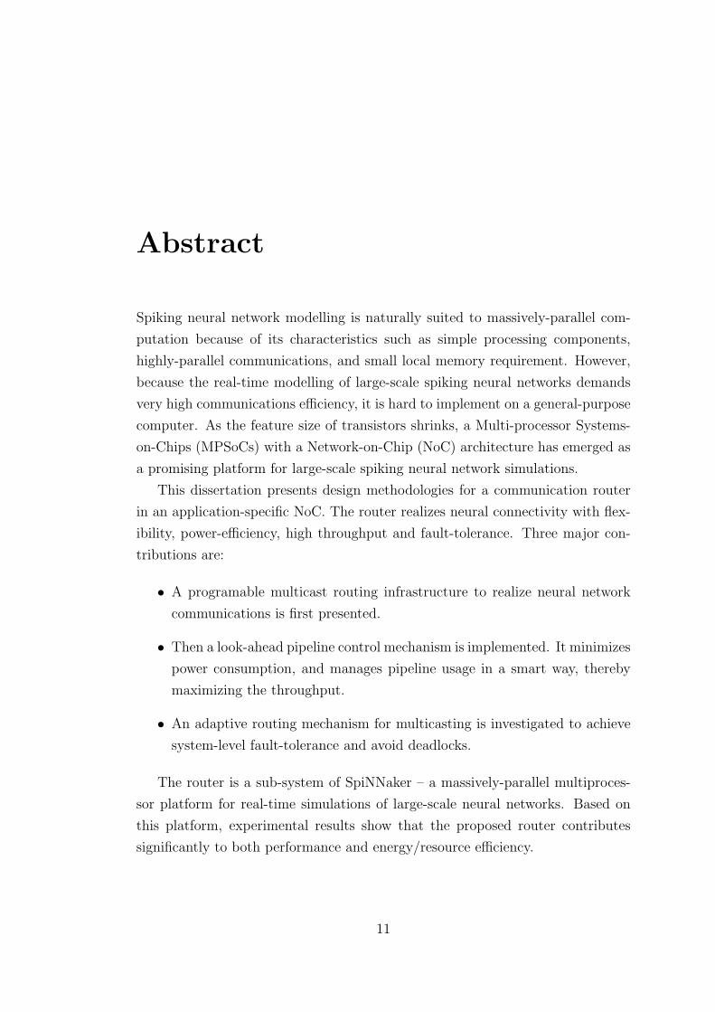
Abstract
Spiking neural network modelling is naturally suited to massively-parallel com-
putation because of its characteristics such as simple processing components,
highly-parallel communications, and small local memory requirement. However,
because the real-time modelling of large-scale spiking neural networks demands
very high communications efficiency, it is hard to implement on a general-purpose
computer. As the feature size of transistors shrinks, a Multi-processor Systems-
on-Chips (MPSoCs) with a Network-on-Chip (NoC) architecture has emerged as
a promising platform for large-scale spiking neural network simulations.
This dissertation presents design methodologies for a communication router
in an application-specific NoC. The router realizes neural connectivity with flex-
ibility, power-efficiency, high throughput and fault-tolerance. Three major con-
tributions are:
• A programable multicast routing infrastructure to realize neural network
communications is first presented.
• Then a look-ahead pipeline control mechanism is implemented. It minimizes
power consumption, and manages pipeline usage in a smart way, thereby
maximizing the throughput.
• An adaptive routing mechanism for multicasting is investigated to achieve
system-level fault-tolerance and avoid deadlocks.
The router is a sub-system of SpiNNaker – a massively-parallel multiproces-
sor platform for real-time simulations of large-scale neural networks. Based on
this platform, experimental results show that the proposed router contributes
significantly to both performance and energy/resource efficiency.
11

Declaration
No portion of the work referred to in this thesis has been
submitted in support of an application for another degree
or qualification of this or any other university or other
institute of learning.
12

Copyright
i. The author of this thesis (including any appendices and/or schedules to this
thesis) owns any copyright in it (the “Copyright”) and s/he has given The
University of Manchester the right to use such Copyright for any adminis-
trative, promotional, educational and/or teaching purposes.
ii. Copies of this thesis, either in full or in extracts, may be made only in
accordance with the regulations of the John Rylands University Library of
Manchester. Details of these regulations may be obtained from the Librar-
ian. This page must form part of any such copies made.
iii. The ownership of any patents, designs, trade marks and any and all other
intellectual property rights except for the Copyright (the “Intellectual Prop-
erty Rights”) and any reproductions of copyright works, for example graphs
and tables (“Reproductions”), which may be described in this thesis, may
not be owned by the author and may be owned by third parties. Such Intel-
lectual Property Rights and Reproductions cannot and must not be made
available for use without the prior written permission of the owner(s) of the
relevant Intellectual Property Rights and/or Reproductions.
iv. Further information on the conditions under which disclosure, publication
and exploitation of this thesis, the Copyright and any Intellectual Property
Rights and/or Reproductions described in it may take place is available from
the Head of School of School of Computer Science (or the Vice-President).
13

Acknowledgements
I would like to express my deep appreciation to all those who have supported me
in finishing this thesis. I would like to thank first of all my supervisor, Prof. Steve
Furber, for his invaluable insights, inspirations and suggestions. He has given me
great supervision and guidance throughout the course of my research.
I would also like to thank my advisor, Dr. Jim Garside, who helped out
tremendously on my work with his great patience. I am also grateful to Dr.
Viv Woods who has helped me to improve the thesis by giving comments and
proof-reading.
I would also like to extend my gratitude to the people at APT group, especially
to those colleagues who have contributed to the SpiNNaker project (Luis Plana,
Steve Temple, Yebin Shi, too many to list here). I had a great time working with
them and they have been very helpful, giving advice and sharing knowledge with
me.
Finally, and most importantly, I would like to thank my mother, Yuming
Song, father, Yazhou Wu, and brother, Yang Wu, who have always been very
supportive of my goals. Their encouragement was extremely important for me to
complete this long journey.
14
Chapter 1
Introduction
Biological brains are capable of performing many intelligent tasks, such as face
recognition, speech processing and language learning, that conventional compu-
tational systems still find difficult [Vig94][MB90][MC93]. The brain is a comput-
ing system which exploits massive parallelism, with limited elemental processing
speed. Here, a huge number of slow, simple elements execute in parallel and
exhibit remarkable characteristics. It is natural for scientists seeking engineered
solutions to the above tasks to consider mimicking the neural networks of bio-
logical brains. However, despite much research into how neural networks work,
knowledge in this area remains limited.
Simulation scale is one of the key factors of neural network modelling. The
simulation of a human brain requires about 100 billion neurons and even more
interconnects. Such a large-scale neural network simulation remains well beyond
the reach of current computation systems, particularly in real-time. The ‘real-
time’ concept means that the simulation finishes no later than do an equal number
of biological neurons performing an equivalent task (which typically means around
1 ms per step) [JSR+97].
The emergence of massively-parallel computational systems offers an oppor-
tunity to bridge the gap between the computational requirements of large-scale
neural networks and the capabilities of relevant platforms. Cluster supercomput-
ers, commonly used by neuroscientists for neural network simulations, are the
current model of conventional parallel systems. These systems are capable of
distributed processing and information storage, thereby delivering high comput-
ing power, but must still overcome the huge demand for data exchange between
processing nodes if a truly real-time simulation is to be achieved.
15
CHAPTER 1. INTRODUCTION 16
As transistor feature sizes continue to shrink, Multi-Processor System-on-Chip
(MPSoC) technology using Network-on-Chip (NoC) communication schemes has
emerged as a promising solution for massively-parallel computing. The appli-
cation of MPSoC technology to conduct research on large-scale spiking neural
network simulations has attracted the attention of both computer engineers and
neuroscientists. An MPSoC has many characteristics similar to those of a spiking
neural network [Con97]:
• They are both parallel systems.
• They both comprise networks of processing components. The basic pro-
cessing element of a neural network is the neuron, which can be described
by relatively simple models, such as the Izhikevich model and the leaky
integrate-and-fire model [Izh03][Tuc88]; the basic processing element of an
MPSoC system is a microprocessor core, usually with a simple architecture
because of energy-efficiency considerations.
• They both have highly parallel connectivity between the processing ele-
ments. A neural network uses many synapses to connect neurons; an MP-
SoC uses an NoC to connect processing cores although it may multiplex
several channels over each physical link.
• They are both event-driven: A spiking neural network communicates using
spike events; an MPSoC communicates using discrete data packets.
The similarity between their characteristics makes the modelling of spiking
neural networks naturally suited to the parallel computations on an MPSoC sys-
tem, making it worthwhile to develop a dedicated MPSoC platform with special
features to support neural network modelling. The platform should enable neu-
roscientists to achieve new insights into the operational principles of neural net-
works by running real-time simulations, with biologically-realistic levels of neural
connectivity. The improved understanding of these natural systems will, per-
haps, inspire computer engineers in their quest for ever-better high-performance
computational architectures.
A neural computation system must achieve balance between its processing,
storage and communication requirements [FTB06]. This dissertation focuses prin-
cipally on the communication issues, and presents the design of a multicast router.
The router is the core communication unit of the SpiNNaker system – a universal
CHAPTER 1. INTRODUCTION 17
spiking neural network simulation platform. The design of the router has to con-
sider both the requirements of supporting neural network communications and
the feasibility of its implementation in an electronic system.
1.1 Neural simulation
Neural simulation addresses the task of understanding the structure of the brain
and applying it to bio-inspired information processing systems [BJ90]. It is one
of the most rapidly developing research fields which attracts psychologists, neu-
roscientists and computer scientists seeking effective solutions to real-world prob-
lems [CW06].
Neural simulation is performed by modelling neural network topologies, which
reflect information transmission between many simple functional elements – the
neurons. The only information issued by a neuron is an electro-chemical im-
pulse, indicating its firing. Information is conveyed by the firing frequency and
the timing of impulses relative to other neurons. The information processing
algorithms of the brain are highly related to the connectivity between neurons.
A major challenge in achieving high performance neural simulation is to emu-
late the connectivity of a biological neural network. It is necessary to provide a
communication infrastructure which models the impulses between neurons.
Wilson compared the neural simulation performance of well-connected versus
loosely coupled processing elements [WGJ01]. The result indicates that commu-
nication latency is the major factor in obtaining good performance, especially in
achieving real-time simulation. An infrastructure specifically supporting the mas-
sive communication of neural networks is therefore desirable for this application-
specific platform. As the central part of this infrastructure, a router that supports
efficient communication of neural impulses is one of the key issues.
1.2 Literature review
Investigations into neural network modelling have been undertaken for several
decades by means of theoretical studies together with experimental simulations.
The research leads to two sub-questions: firstly, how can the brain’s behaviour
be abstracted into computable models which neuroscientists achieve by neural

CHAPTER 1. INTRODUCTION 18
network modelling; secondly, how can this computation be performed on an ar-
tificial platform. Although research into neural modelling has seen remarkable
progress, the second question remains unanswered. Many research projects have
been proposed in the area of developing neural simulation platforms.
1.2.1 Software neural simulators
Many software simulators, such as GENESIS and NEURON, can be used to
model neurons with high biophysical realism and are flexible as a result of their
programmability [BB98][HC97]. They provide interfaces to conventional com-
puters: general-purpose workstations initially and, later, commercially-available
computer clusters to achieve larger simulation scales. However, software simula-
tors are inefficient for neural modelling, especially for large-scale networks. One
major reason is that spike propagation in neural networks is inherently event-
driven whereas software simulators typically employ time-driven models [Moi06].
1.2.2 Neural simulations on general-purpose computers
General-purpose stand-alone workstations are the most commonly used platforms
for neural simulations because they are economical, easily available and con-
venient to program. State-of-the-art processors have adequate computational
power to support a certain scale of neural simulation in real time. For example,
Boucheny presented a complete physiologically-relevant spiking cerebellum model
that runs in real-time on a dual-processor computer. The model consists of 2,000
neurons and more than 50,000 synapses [BCRC05]. However, neural networks
modelled on sequential computers are constrained to be very small-scale due to
the limitations of the computational resource. This narrows the application range.
The pursuit of performing larger-scale neural simulations has led to investiga-
tions into hardware integration. As neural networks are inherently parallel sys-
tems, larger-scale simulations are suitable to be performed on parallel computers.
Several spiking neural networks have been implemented on commercially-available
parallel computers, such as the Transputer array used at Edinburgh [FRS+87], the
CM-2 Connection Machine developed by Thinking Machines Corporation [Moi06].
With the advances in computational power, concurrent hardware implementa-
tions are adequate for simulating very large neural networks. A current, on-going
example is the Blue Brain project conceived at IBM [Mar06]. It can simulate up
CHAPTER 1. INTRODUCTION 19
to 100,000 highly complex neurons or 100 million simple neurons, which corre-
sponds to the number of neurons in a mouse brain.
Computation power is available because the neural simulation problem is lin-
early scalable. A parallel computer architecture distributes computational tasks
onto different processing elements to decrease the workload on an individual pro-
cessor so that it fulfills the neural simulation’s requirements in terms of scale
and computational power. However, communication overheads in existing par-
allel architectures limit the overall execution speed of large-scale spiking neu-
ral simulations, which is a crucial requirement for the accomplishment of many
bio-realistic tasks, such as real-time vision detection. Parallel computer archi-
tectures struggle to reach the requirements of real-time simulation (1 ms resolu-
tion) [PEM+07]. This is because existing architectures are not designed to cope
with communication scalability as ‘conventional’ software doesn’t require it. Of
the above cases, only the CM-2 achieved real-time simulation of a spiking neural
network, with a scale up to 512K neurons [JSR+97]. Unfortunately, a network
of even several thousand neurons is still too small to satisfy the needs of many
application-specific simulations and large-scale parallel computers usually have
high maintenance costs.
1.2.3 Neurocomputers
Because of the limitation of running a fast simulations of a large-scale spiking
neural network on general-purpose high-performance computers, there is a mo-
tivation for developing dedicated digital hardware – so-called neurocomputers –
which aim to achieve more cost-effective performance and faster simulation speed.
They are usually custom built to distribute processing and storage, and are im-
plemented with neurochips or a conventional computer plus neural accelerator
boards that optimize the simulation algorithm.
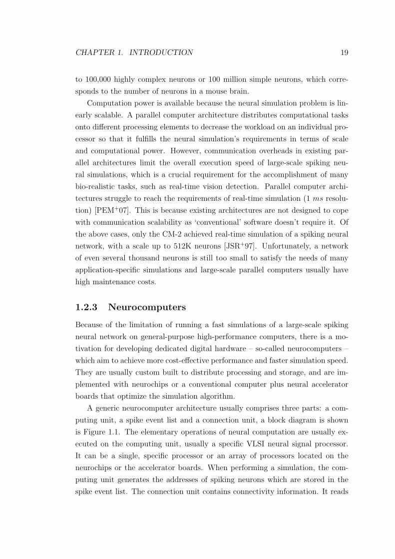
A generic neurocomputer architecture usually comprises three parts: a com-
puting unit, a spike event list and a connection unit, a block diagram is shown
is Figure 1.1. The elementary operations of neural computation are usually ex-
ecuted on the computing unit, usually a specific VLSI neural signal processor.
It can be a single, specific processor or an array of processors located on the
neurochips or the accelerator boards. When performing a simulation, the com-
puting unit generates the addresses of spiking neurons which are stored in the
spike event list. The connection unit contains connectivity information. It reads

CHAPTER 1. INTRODUCTION 20
Communicationunit
Spikelist
Target neurons
Spiking neurons Computation
unit
Figure 1.1: A generic neurocomputer
the address of a neural spike from the spike event list and derives the address of
target neurons [Ram92]. Well-known examples include NESPINN, CNAPS and
SYNAPSE.
NESPINN (Neurocomputer for Spiking Neural Networks) was designed at the
Institute of Microelectronics of the Technical University of Berlin [SMJK98]. Its
block diagram is shown in Figure 1.2. The system was designed specifically for
spiking neural networks. A NESPINN board is capable of simulating up to 512K
spiking neurons with up to 104 connections. It consists of one connection chip
and one processing chip. The connection chip holds the network topology. The
processing chip has several processing elements, each of which executes a partition
of the whole neural network. The NESPINN board achieves a good performance
by using an efficient neuron parallel mapping scheme and a mixed dataflow/SIMD
(Single Instruction Multiple Data) mode in the architecture. However, its has
limited scalability.
The CNAPS (Connected Network of Adaptive Processors) system, proposed
at Adaptive Solutions, has shown a certain level of scalability [Ham91]. Its block
diagram is shown in Figure 1.3. The elementary functional block of the CNAPS
system is a neurochip, N6400, which contains 64 processing elements. A system
can be expanded via a broadcast interconnection scheme, where a maximum

CHAPTER 1. INTRODUCTION 21
Connectionchip
Spikelist chip
NESPINN
Memory
Figure 1.2: NESPINN
8−bit data bus
32−bit data bus
Controlprocessor
CNAPSarray chip
CNAPSarray chip
CNAPSarray chip
Figure 1.3: CNAPS
of eight chips with a total of 512 processing elements are connected by two 8-
bit broadcast buses in a SIMD mode. Any information exchange between the
neurochips is transferred via the buses, which makes them system bottlenecks.
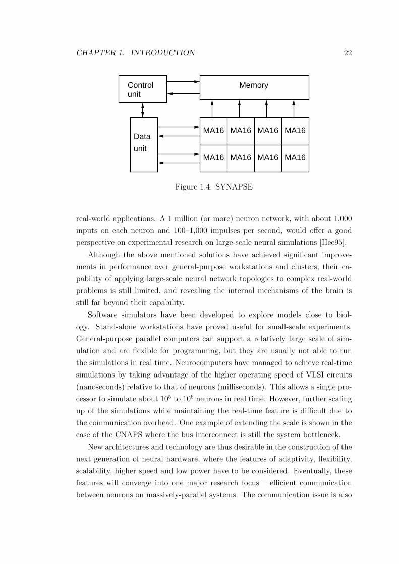
The neurocomputer SYNAPSE (Synthesis of Neural Algorithms on a Parallel
Systolic Engine), developed at Siemens, also consists of eight neurochips (MA-16),
connected by a systolic ring architecture [RRH+95]. Its block diagram is shown
in Figure 1.4. The throughput of the communication channels is optimized by
pipelining. However, the systolic ring architecture is also considered non-scalable.
1.2.4 Limitations of previous neural simulators
Due to the high diversity of applications, there are many algorithms for neural
networks. For example, some applications focus on real-time interactions, such
as robot control, others focus on the exploration of neural modelling or brain
function. It is, therefore, hard to develop a general benchmark for all neural
simulations. However, one straightforward, and perhaps the simplest, way of ex-
amining the effectiveness of neural simulations is to evaluate their performance on
CHAPTER 1. INTRODUCTION 22
MA16 MA16 MA16
MA16MA16MA16MA16
MA16Data
unit
MemoryControlunit
Figure 1.4: SYNAPSE
real-world applications. A 1 million (or more) neuron network, with about 1,000
inputs on each neuron and 100–1,000 impulses per second, would offer a good
perspective on experimental research on large-scale neural simulations [Hee95].
Although the above mentioned solutions have achieved significant improve-
ments in performance over general-purpose workstations and clusters, their ca-
pability of applying large-scale neural network topologies to complex real-world
problems is still limited, and revealing the internal mechanisms of the brain is
still far beyond their capability.
Software simulators have been developed to explore models close to biol-
ogy. Stand-alone workstations have proved useful for small-scale experiments.
General-purpose parallel computers can support a relatively large scale of sim-
ulation and are flexible for programming, but they are usually not able to run
the simulations in real time. Neurocomputers have managed to achieve real-time
simulations by taking advantage of the higher operating speed of VLSI circuits
(nanoseconds) relative to that of neurons (milliseconds). This allows a single pro-
cessor to simulate about 105 to 106 neurons in real time. However, further scaling
up of the simulations while maintaining the real-time feature is difficult due to
the communication overhead. One example of extending the scale is shown in the
case of the CNAPS where the bus interconnect is still the system bottleneck.
New architectures and technology are thus desirable in the construction of the
next generation of neural hardware, where the features of adaptivity, flexibility,
scalability, higher speed and low power have to be considered. Eventually, these
features will converge into one major research focus – efficient communication
between neurons on massively-parallel systems. The communication issue is also

CHAPTER 1. INTRODUCTION 23
becoming one of the central topics of the trend of research on new computer
paradigms, which aim to make multi-core processing on one or several chips
feasible.
1.3 Design considerations
Biological neurons are massively interconnected but ‘compute’ slowly (less than ∼1,000 Hz) and communication speed is low (∼ 1 ms). Electronic components are
much faster (several GHz) but interconnection is expensive. However several dig-
ital neural impulses can be multiplexed over a communication channel to provide
similar connectivity to biological neurons.
An ARM968 processor is capable of simulating ∼ 1,000 neurons and the as-
sociated synapses connections in real time with ∼ 50 MB memory [JFW08]. In
a system which scales to one million neurons around 1,000 microprocessors are
needed, producing around one billion impulses per second. This requires an inter-
connection network able to handle a large number of neural impulses in real-time.
This dissertation focuses on a router as the central communication unit of
the interconnection network. A set of issues were considered in designing the
architecture of the router to fulfill the communication requirements of neural
modelling as well as those of massively-parallel system configurations.
Three routing algorithms are defined as the basic functionalities: multicast
routing for neural impulses transmission; point-to-point routing for system man-
agement and control information transmission; and nearest-neighbour routing
for boot-time, flood-fill and chip debug information transmission. The multicast
routing is the principal function of the router. It is more efficient for neural
communication than typical unicast and broadcast routing because neurons have
high fan-outs.
Some fault-tolerance features are considered for inclusion in the router. This
is an emulation of biological systems which have certain abilities to identify and
isolate faults.
The design is optimized to significantly reduce power and area consumption so
that the router can handle a large number of neural impulses with low overhead.

CHAPTER 1. INTRODUCTION 24
1.4 Contributions
This dissertation focuses on the investigation of a novel router architecture for
the real-time modelling of spiking neural networks on a massively-parallel system
via an on/inter-chip communication infrastructure. The router supports multiple
routing algorithms which are designed specifically for efficient communication in
large-scale neural networks. The major contributions include:
• Communication efficiency: Neural networks may be modelled in real time
by taking advantage of the massive parallelization of the platform. This is
achieved by properly balancing the system resources between computation,
storage and communication. The design effort described in this dissertation
focuses on deriving higher communication efficiency, principally through the
multicast routing of neural packets.
• System scalability: Biological neural networks range from small-scale sys-
tems with several neurons to very large-scale systems with tremendous num-
bers of neurons. A platform for neural network modelling must be scalable,
so that the same algorithm can be applied to various neural networks. To
achieve a better scalability and speed than conventional buses, a router in
a Network-on-Chip architecture is used for on-chip neural message routing
and processing elements organization. In this way, the platform is formed
from an array of neural chips, wrapped into a torus.
• Fault-tolerance: Fault-tolerance has become increasingly crucial in VLSI
design as device variability becomes an inevitable issue in deep sub-micron
technology. It is, however, present in most biological systems. The scale
of the system requires an adaptive routing mechanism to enhance system-
level fault-tolerance. An error handling mechanism is applied to enhance
the reliability of data flows.
• Power/area efficiency: On-chip network design needs more consideration
of energy and area efficiency than macro networks. These issues become
even more important as a power/area-intensive associative memory circuit
is required for the neural platform to store spiking neuron addresses.
• Universality: The system is intended to support multiple neural models,
and can be configured ‘on the fly’. This is realized by taking advantage of
CHAPTER 1. INTRODUCTION 25
the higher flexibility of programmable digital hardware. Configuration of a
distributed system requires message passing between the processing nodes,
which is accomplished by multiplexing the neural communication channel
of the router and requires proper design of the transaction protocols.
1.5 Dissertation organization
The organization of this dissertation is as follows: After discussing the basic
concepts of neuron modelling in chapter 2, the thesis starts with discussing the
feasibility of applying the Network-on-Chip approach to the implementation of
a neurocomputing platform (chapter 3), and then particularly focuses towards
the communication issues of the platform in chapter 4. Chapter 5 presents the
architectural considerations of the router, which is the heart of the system’s com-
munication network. Detailed implementations of the router’s routing algorithms
follow in chapter 6. Chapter 7 presents router pipelining for flow control and
power saving. Following that in chapter 8 the router’s performance is evalu-
ated from several perspectives, including its basic functions, its behaviours in a
network environment, packet drop rate, power consumption and circuit area. Fi-
nally, in chapter 9, conclusions are drawn about how the design demonstrates the
advantages and disadvantages of the proposed routing strategy for a large-scale
neural platform in addition to suggesting future explorations and optimizations.
1.6 Publications
The following papers have been published or submitted for publication, based on
the work presented in this dissertation.
• Wu, J. and Furber, S.B.,
Delay insensitive chip-to-chip interconnect using incomplete 2-of-7 NRZ
data encoding [WF06]
(18th UK Asynchronous Forum)
The paper introduces the concepts and implementations of delay-insensitive
signalling protocols for a chip interface which extends the router’s on-chip
links into inter-chip links, followed with evaluations of the performance;
• Wu, J., Furber, S.B. and Garside, J.D.
CHAPTER 1. INTRODUCTION 26
A programmable adaptive router for a GALS parallel system [WFG09]
(15th IEEE International Symposium on Asynchronous Circuits and Sys-
tems)
The paper demonstrates the design implementation of the router in the
SpiNNaker system. It proves the design feasibility and addresses the im-
portant issues desired by a neural simulation platform, such as programma-
bility, adaptivity and scalability (see chapters 6, 7 and 8);
• Wu, J. and Furber, S.B.
A multicast routing scheme for a universal spiking neural network architec-
ture [WF09]
(The Computer Journal)
The paper discusses the design considerations of the router from a neural
simulation point of view. It addresses the importance of communication
efficiency to neural network modelling, followed by evaluation results of
power saving and adaptive routing showing the significance of the design
(see chapter 5, 6 and 8);
• Plana, L.A., Furber, S.B., Temple, S., Khan, M., Shi, Y., Wu, J. and Yang,
S.
A GALS infrastructure for a massively parallel multiprocessor [PFT+07]
(IEEE Design and Test of Computers)
The paper focuses on the GALS infrastructure of the SpiNNaker system
and describes the router as a crucial part of the infrastructure (see chapter
4);
• Plana, L.A., Furber, S.B. Bainbridge, J., Salisbury, S., Shi, Y. and Wu, J.
An on-chip and inter-chip communications network for the SpiNNaker massively-
parallel neural net simulator [PFB+08]
(The 2nd IEEE International Symposium on Network-on-Chip)
The poster provides a perspective of the SpiNNaker system (see chapter 4);
• Lujan, M., Furber, S.B., Jin, X., Khan, M., Lester, D., Miguel-Alonsoy, J.,
Navaridasy, J., Painkras, E., Plana, L.A., Rast, A., Richards, D., Shi, Y.,
Temple, S., Wu, J. and Yang, S.
Fault-tolerance in the SpiNNaker architecture (submitted)
(IEEE Transactions on Computers)

CHAPTER 1. INTRODUCTION 27
The paper addresses the fault-tolerance feature considered in the design of
the SpiNNaker platform, where the router is one of the key components
supporting this feature. A case study has been carried out using a 256 ×256 2-dimensional triangular mesh. It shows the router’s adaptive rout-
ing mechanism can significantly enhance system-level fault-tolerance and
stability by decreasing the packet drop rate (see chapter 8).
Chapter 2
Neurcomputing
This chapter introduces the biological and mathematical background of neur-
computing. The knowledge presented here includes neurocomputing’s principles,
characteristics, and possible implementation methods, to explain the theoretical
foundations for implementing neurocomputing through a VLSI approach. Follow-
ing that spiking neural networks and one of the spiking neural models, Izhikevich
model, are introduced. The feature of spiking neural networks shows that it is
possible to model the networks in real-time. This brings challenges to the develop-
ment of an efficient communication mechanism which will be further investigated
in the following chapters.
2.1 Introduction
The biological brain, which features high complexity, nonlinearity, and massive
parallelism, is the central unit of the nervous system. It makes appropriate de-
cisions in many intelligent tasks, such as speech recognition, image analysis, and
adaptive control.
Research to understand the brain started from 1911 when Ramon y Cajal first
introduced the concept of neurons as basic operational elements of the neural
network. A brain contains a huge number of neurons. It is estimated that there
are 100 million neurons in the mouse brain and 100 billion neurons in the human
brain. They are massively interconnected by junctions called synapses and form
a neural network. The operations of the brain are represented by the activities of
the neural network, which is further represented by those of the individual neurons
and their interactions. Neurons operate at a slower process speed than silicon logic
28
CHAPTER 2. NEURCOMPUTING 29
gates [Hay98], however, a huge number of these slow, simple elements exhibit
some remarkable characteristics by evaluating in parallel. The brain also has
significantly lower power consumption (10−16 Joules per operation), an energy
budget that the human body can afford.
In computer science, the modelling of artificial neural networks is called neu-
rocomputing and intends to reflect complex relationships between the network’s
inputs and outputs. Haykin’s book provides a comprehensive survey of neural
network characteristics distinguishing neurocomputing from conventional compu-
tation [Hay98].
• Nonlinearity – An artificial neural network can be a nonlinear system which
is inherently suitable for processing certain signals with nonlinearity (e.g.
speech signals).
• Input-output mapping – A set of samples with unique inputs and the cor-
responding desired outputs can be applied to a neural network for training
purposes. The network is modified in response to the examples so that it
is finally trained to generate output with acceptable difference from the de-
sired results. Thus mapping relationships between input and output signals
of selected examples can be constructed within the network.
• Adaptivity – A neural network is naturally adaptive to its operating envi-
ronment which it achieves by the real-time modification of synaptic weights.
• Fault tolerance – Brains are fault tolerant: neurons die continuously yet the
brain (largely) continues to function. A hardware implementation of a neu-
ral network is potentially capable of maintaining functionality by degrading
its performance to an acceptable extent rather than displaying catastrophic
failure when facing damage.
• Evidential response – A neural network displays a high level of confidence in
pattern recognition. This means it is not only able to recognise particular
patterns, but also may be used to reject ambiguous patterns.
• Contextual information – A neural network is inherently capable of pro-
cessing contextual information. The knowledge representation of a neural
network is based on its structure and activation state.
CHAPTER 2. NEURCOMPUTING 30
• VLSI implementability – A neural network is well suited for implementation
using VLSI because of its massively-parallel nature.
• Uniformity of analysis and design – Neural networks share common theories
and learning algorithms. It is credible to use the same notation in all
domains.
• Neurobiological analogy – Research into neural networks provides an op-
portunity for interpreting neurobiological phenomena. The improved un-
derstanding of the natural phenomena will, in turn, inspire engineers in
their quest for ever-better high-performance computational architectures.
The above-mentioned characteristics of neurocomputing suggest great engi-
neering perspectives, but a implementation of the computation requires a pro-
found understanding of how a neural network works. The remainder of this
chapter presents the basic knowledge of neurocomputing, which starts with the
biological characteristics of neural networks, followed by the mathematical mod-
elling of neurons and neural networks, and ending up with the introduction of
spiking neural networks which may be suitable for large-scale, real-time modelling
on VLSI.
2.2 Biological neurons and neural networks
The first step towards understanding the principles of neurocomputing is to un-
derstand the behaviour of the individual biological neuron. Biological neurons are
the elementary functional devices of neural networks, they perform their functions
by processing and transmitting/receiving impulses between each other.
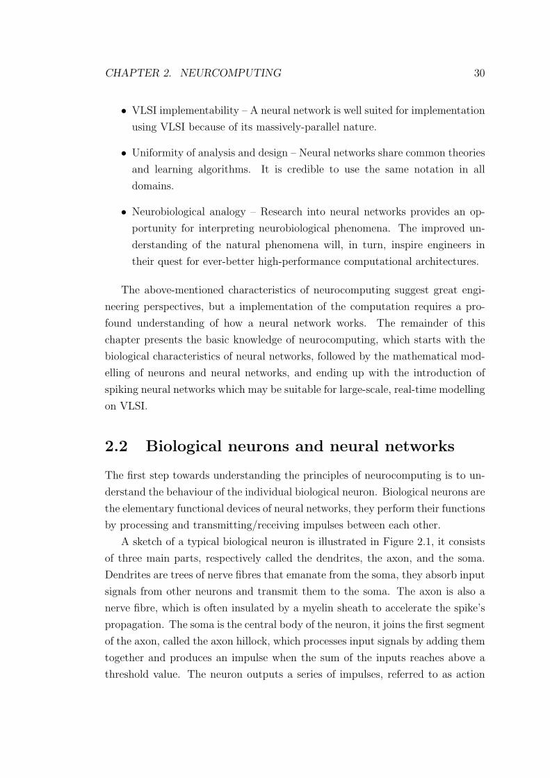
A sketch of a typical biological neuron is illustrated in Figure 2.1, it consists
of three main parts, respectively called the dendrites, the axon, and the soma.
Dendrites are trees of nerve fibres that emanate from the soma, they absorb input
signals from other neurons and transmit them to the soma. The axon is also a
nerve fibre, which is often insulated by a myelin sheath to accelerate the spike’s
propagation. The soma is the central body of the neuron, it joins the first segment
of the axon, called the axon hillock, which processes input signals by adding them
together and produces an impulse when the sum of the inputs reaches above a
threshold value. The neuron outputs a series of impulses, referred to as action
CHAPTER 2. NEURCOMPUTING 31
Synapse
Axon
Dendrites
Soma
Axon hillock
Axon terminals
− Presynaptic axon terminal membrane
− Postsynaptic dendrite membrane
Figure 2.1: Biological neuron
potentials or spikes which are conveyed to their many target terminals to other
neurons via the neuron’s axon.
There are junctions, known as synapses, between the neuron terminals and
the dendrites of other neurons. A synapse couples the presynaptic axon terminal
membrane and the postsynaptic dendrite membrane together and maintains the
strength of their interactions by the state of electrical polarization. It performs
complex signal processing by dynamically converting a presynaptic signal, which
it receives from one neuron, into a postsynaptic signal (PSP) [MHM96]. This
is done by weighting the incoming spikes by their respective synaptic efficacies
which it passes to the axon hillock via the dendrites. This signal processing
procedure is crucial in learning and adaptation.
Each neuron usually has 1,000 to 10,000 synapses. The many synaptic links
assemble the neurons into a massively interconnected neural network. This mas-
sive interconnection produces many presynaptic signal to a neuron. However, a
presynaptic signal can be regarded as a digital signal which either presents or
not, so it is possible to model the interconnection on a digital VLSI system. The
modelling of the interconnection is the major topic of this thesis.
Many PSPs are summed together in the axon hillock with the result expressed
as the membrane potential. If the potential exceeds a threshold (v), the cell
body will initiate an action potential to its target synapses via the neuron’s
CHAPTER 2. NEURCOMPUTING 32
axon [Gur97]. These procedures are the typical activities of an individual biolog-
ical neuron. Research into biological neurons makes it possible to represent and
compute their activities using mathematical neurobiology.
2.3 Mathematical neurobiology
Mathematical neurobiology is the methodology of abstracting neural activities
into computable models which capture the essential information-processing fea-
tures of real neurons. This methodology, also called neural modelling, forms the
basis for designing the artificial neural network [Hay98].
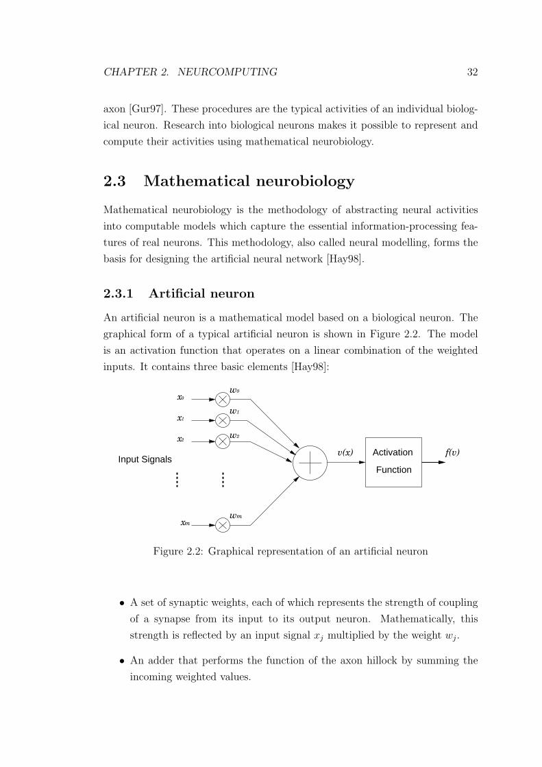
2.3.1 Artificial neuron
An artificial neuron is a mathematical model based on a biological neuron. The
graphical form of a typical artificial neuron is shown in Figure 2.2. The model
is an activation function that operates on a linear combination of the weighted
inputs. It contains three basic elements [Hay98]:
v(x)
x
w
Input SignalsActivation
Function
f(v)
w
w
xwm
x
0
1
2
x0
1
2
m
Figure 2.2: Graphical representation of an artificial neuron
• A set of synaptic weights, each of which represents the strength of coupling
of a synapse from its input to its output neuron. Mathematically, this
strength is reflected by an input signal xj multiplied by the weight wj.
• An adder that performs the function of the axon hillock by summing the
incoming weighted values.
CHAPTER 2. NEURCOMPUTING 33
• An activation function that induces an output action potential when the
summed weights reach a predetermined threshold. The activation function
is different in different models.
The development of neural modelling has been classified into three generations
with different levels of biological realism, relating to different types of neural
network [Vre02].
The first generation of neuron model was proposed by McCulloch and Pitts
in 1943. In the McCulloch-Pitts model, the activation function is a squashing
function producing a Boolean value.
Mathematically, the McCulloch-Pitts model can be described by the pair of
equations below:
v(x) =m∑
j=0
wjxj (2.1)
f(v) =
1 if v ≥ 0
0 if v < 0
This model provides the possibility of building a machine with the ability to
learn from experience [VSVJ89].
The second generation of neuron uses a continuous activation function to com-
pute the output. Unlike the first generation, whose activation function generates
a digital output, the second generation is suitable for analog in- and output.
The third generation of neuron is the spiking neuron, which will be introduced
latter in a separate section.
Artificial neurons are the elementary operational units of an artificial neural
network. Each of the neurons computes weighted inputs from the outputs of the
other neurons according to the activation function. The operation of an artificial
neural network is not merely represented by individual neuron models. It is also
related to the interconnections between neurons.
2.3.2 Artificial neural networks
An artificial neural network is a collection of interconnected mathematical neuron
models, performing computational modelling of biological networks. With the

CHAPTER 2. NEURCOMPUTING 34
massively-connected simple neuron models, the neural network exhibits complex
global behaviours.
In mathematical terms, the neural network’s logic structure is represented
by the composition of a set of functions. A function f(v) which represents the
output of a neuron model is composed of other functions v(x), which can further
be composed of other weighted inputs (x0 to xm). The weights can be adjusted
so that they adapt the network’s logic structure dynamically to a certain learning
algorithm during the training phase. The design of the artificial neural network
has to be determined by these algorithms.
A signal-flow graph [Mas56], which principally focuses on the depiction of the
relationships (represented by a set of arrows) between neurons (represented by a
set of nodes), can also represent an artificial neural network.
Input Layer Middle Layer 1 Middle Layer 2 Output Layer
N2
N3
Nm
N1 N1
N3
N2
Nx
N1
N2
N3
N1
N2
N3
Ny Nz
Figure 2.3: Layer structured neural network
The neurons are normally arranged in a layered structure, in which layers
are defined as the input layer, the hidden layer(s), and the output layer. The
input layer supplies the source of the input signals which are applied to the
computation nodes in the hidden layer. The outputs of the hidden layer(s) are
finally computed by the output layer to issue the output of the network. There are
three categories of neural network architecture: single-layer feedforward networks,
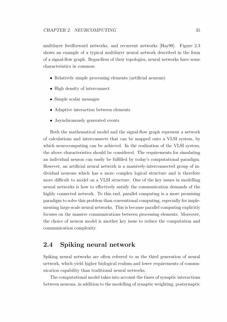
CHAPTER 2. NEURCOMPUTING 35
multilayer feedforward networks, and recurrent networks [Hay98]. Figure 2.3
shows an example of a typical multilayer neural network described in the form
of a signal-flow graph. Regardless of their topologies, neural networks have some
characteristics in common:
• Relatively simple processing elements (artificial neurons)
• High density of interconnect
• Simple scalar messages
• Adaptive interaction between elements
• Asynchronously generated events
Both the mathematical model and the signal-flow graph represent a network
of calculations and interconnects that can be mapped onto a VLSI system, by
which neurocomputing can be achieved. In the realization of the VLSI system,
the above characteristics should be considered. The requirements for simulating
an individual neuron can easily be fulfilled by today’s computational paradigm.
However, an artificial neural network is a massively-interconnected group of in-
dividual neurons which has a more complex logical structure and is therefore
more difficult to model on a VLSI structure. One of the key issues in modelling
neural networks is how to effectively satisfy the communication demands of the
highly connected network. To this end, parallel computing is a more promising
paradigm to solve this problem than conventional computing, especially for imple-
menting large-scale neural networks. This is because parallel computing explicitly
focuses on the massive communications between processing elements. Moreover,
the choice of neuron model is another key issue to reduce the computation and
communication complexity.
2.4 Spiking neural network
Spiking neural networks are often referred to as the third generation of neural
network, which yield higher biological realism and lower requirements of commu-
nication capability than traditional neural networks.
The computational model takes into account the times of synaptic interactions
between neurons, in addition to the modelling of synaptic weighting, postsynaptic
CHAPTER 2. NEURCOMPUTING 36
summation and activation. Hence, spiking neural networks are not only suitable
for information processing, like conventional neural networks, they can also be
used for the exploration of biological inspired architecture [Moi06].
Communication is based on a dynamic event-driven scheme. Neurons do not
produce spikes at every propagation cycle; only a few neurons are active when
their membrane potentials reach a threshold. It is possible to convey these spikes
using small packets. In addition, the packets can be clustered when transmitting
because many spikes usually share a same destination. These reduce the commu-
nication costs and makes the simulation of spiking neural networks well suited to
VLSI implementations.
2.4.1 Generations of spiking neural models
The spiking neuron model was first proposed by Hodgkin and Huxley in 1952.
This is an accurate biological model which describes the detailed process of gen-
erating and propagating action potentials. Similar types of model include the
integrate-and-fire, FitzHugh-Nagumo and Hindmarsh-Rose models, etc.
Accurate neuron models are computationally very complex. They are not
practical for large-scale real-time simulations because of constrained hardware
resources. In recent years, various spiking neuron models have been proposed
which are computationally simpler as they capture only the principal information
processing aspects of the neuron’s function and omit other complex biological
features.
2.4.2 Izhikevich model
The Izhikevich model is one of the simplified spiking neuron models, but providing
a certain accuracy for biological neuron modelling. It exhibits firing patterns of all
known types of cortical neuron by appropriate setting of the parameters [Izh04].
The model can be used to simulate spiking cortical neurons in real time [Izh03].
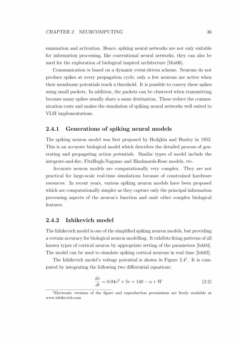
The Izhikevich model’s voltage potential is shown in Figure 2.41. It is com-
puted by integrating the following two differential equations:
dv
dt= 0.04v2 + 5v + 140− u + W (2.2)
1Electronic versions of the figure and reproduction permissions are freely available atwww.izhikevich.com
CHAPTER 2. NEURCOMPUTING 37
peak 30
reset c
reset ddecay with rate a
sensitivity b
v(t)
u
W
(t)
Figure 2.4: Izhikevich model’s voltage potential
du
dt= a(bv − u) (2.3)
In the above equations, v represents the activation potential; u represents
the recovery variable; W is the sum of the weighted inputs, delivering synaptic
currents or injected DC currents; a and b are abstract parameters of the model.
When the voltage exceeds a threshold value (preset at 30), both v and u are
reset:
if v ≥ 30, then
v ← c
u← u + d
where c and d are dimensionless parameters.
In the simulation of the model, neurons are updated every millisecond. At
that point when a pre-synaptic neuron issues an input spike, and the spike arrives
at the post-synaptic neuron, the synaptic weight of the connection between the
two neurons will be added to the input current W [JFW08].
2.5 Summary
Neurocomputing provides high computational power and a wide range of ap-
plication as well as an opportunity of better understanding the principles of the
brain. This chapter has illustrated how simple models have been developed which
(apparently) represent the actions of neurons and synapses. There is also some
indication of how interconnectivity can be represented, simply by ‘wiring’ outputs

CHAPTER 2. NEURCOMPUTING 38
to input synapses. The next chapter will discuss a feasible way of emulating the
massive communication of neurons on silicon.
Chapter 3
Networks-on-Chip
The continuing shrinkage of feature size has increased the computing power avail-
able on a single chip to almost embarrassing levels. Indeed integration levels
appear to have surpassed those exploitable by single, conventional processors,
and multicore CPUs are becoming the norm. Although these introduce their
own problems – at least to conventional programming models – this abundance
of computing power has opened up numerous new opportunities, e.g. efficient
modelling of large-scale neural networks. The ‘cleverness’ of a brain is believed
to be a feature of its connectivity; it is therefore necessary to provide some form
of communications infrastructure so that neurons modelled on a processing net-
work can transmit impulses to each other. This chapter discusses the perspective
of applying the NoC approach to the construction of a digital large-scale neural
network simulator. A NoC platform has a router-based packet-switching commu-
nication network which is believed to be a more promising solution for complex
on-chip interconnect than conventional synchronous bus architectures.
3.1 Introduction
The number of transistors per chip has already hit the billion mark and will keep
growing, whilst many high-performance processor cores still utilise a small num-
ber of transistors for the sake of power-efficiency; for example, an ARM9TDMI
processor only has about 112K transistors [Mac97]. The simplicity of such pro-
cessor cores allows a single die to accommodate tens to hundreds or even thou-
sands of cores to gain higher computational power. This forms a multi-processor
System-on-Chip (MPSoC) which has been recognized as a promising candidate
39

CHAPTER 3. NETWORKS-ON-CHIP 40
technology to drive the advance of the semiconductor industry.
An MPSoC typically comprises processing units such as processing cores, Digi-
tal Signal Processors (DSPs), Field-Programmable Gate Arrays (FPGAs), storage
units such as RAMs, ROMs and Content-Addressable Memories (CAMs) and in-
terconnect units such as buses, routers and switches. As the delay and the power
consumption of global interconnects is becoming more significant than that of
transistors as technology scales, on-chip interconnect has become the bottleneck
of MPSoC architectures. One challenge facing future research into MPSoCs is
posed by the demands for novel architectures which can better support the trend
towards high parallelism. In recent years, research into cost-effective on-chip in-
terconnect has been given increasing attention as it is regarded as the key issue
in achieving MPSoC parallelism.
Processor
Processor
RAM
DSP
FPGA
Router/Switch
Router/Switch
Router/Switch
Router/Switch
Router/Switch
Router/Switch
Router/Switch
Figure 3.1: An MPSoC based on NoC
Commercially-available on-chip interconnect solutions are mostly bus-based
architectures, e.g. ARM AMBA [Mac97]. Although a bus is efficient in broad-
casting, it does not have good scalability to maintain high bandwidth and high
clock frequency [LYJ06]. As the complexity of interconnect keeps growing, re-
search focus has shifted towards the development of micro-networks, collectively
called Networks-on-Chip (NoCs), which are potentially more suitable for parallel
systems and better fit the tight resource chip area and power budget.
The principle of micro-networks is borrowed from conventional computer net-
works [DBG+03], where the distributed processing and storage units are coupled
CHAPTER 3. NETWORKS-ON-CHIP 41
by a set of routers and switches, joined together via link channels. Each router
or switch has a set of ports which connect it to its neighbours and to the local
processing and storage units. An example of a NoC-based MPSoC is shown in
Figure 3.1. The NoC approach brings potential benefits as well as challenges to
MPSoC designers. These will be explained in the following sections.
3.2 Benefits of adopting NoCs
For large-scale on-chip interconnect, the NoC approach offers at least three useful
advantages for MPSoCs:
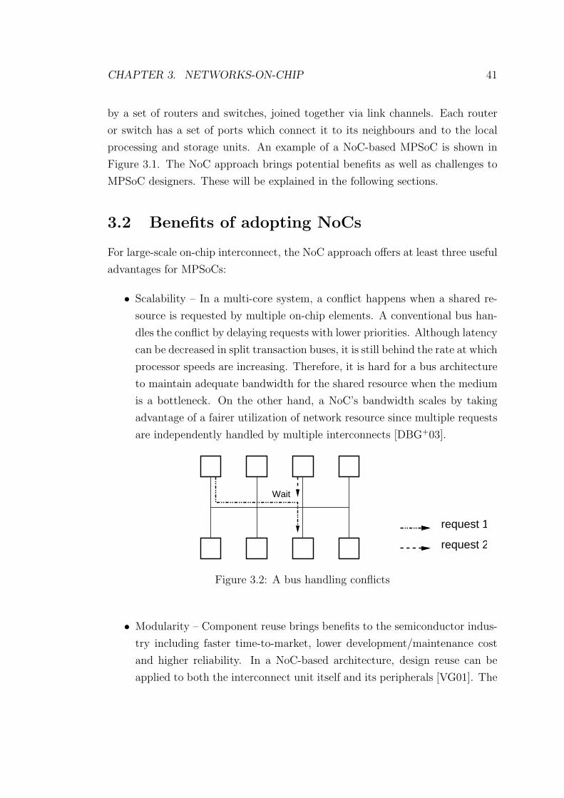
• Scalability – In a multi-core system, a conflict happens when a shared re-
source is requested by multiple on-chip elements. A conventional bus han-
dles the conflict by delaying requests with lower priorities. Although latency
can be decreased in split transaction buses, it is still behind the rate at which
processor speeds are increasing. Therefore, it is hard for a bus architecture
to maintain adequate bandwidth for the shared resource when the medium
is a bottleneck. On the other hand, a NoC’s bandwidth scales by taking
advantage of a fairer utilization of network resource since multiple requests
are independently handled by multiple interconnects [DBG+03].
Wait
request 1
request 2
Figure 3.2: A bus handling conflicts
• Modularity – Component reuse brings benefits to the semiconductor indus-
try including faster time-to-market, lower development/maintenance cost
and higher reliability. In a NoC-based architecture, design reuse can be
applied to both the interconnect unit itself and its peripherals [VG01]. The

CHAPTER 3. NETWORKS-ON-CHIP 42
reuse of the interconnect unit is realised by generalizing its design and syn-
thesis process and providing customizable switching/routing engines. Net-
work interfaces and transaction protocols have to be standarized to facilitate
the reuse of the peripherals, e.g. the processor cores and the memory blocks.
• Fault-tolerance – The construction of a large, complex system requires that
many reliability challenges be faced, especially when the chip fabrication
steps into deep sub-micron technologies. A ‘fault-tolerance’ characteristic
is therefore desirable, which enables a system to keep functioning when
encountering transient or permanent hardware failure. A NoC structure
offers the potential of reconfiguring the hardware resource allocation to
achieve system-level fault-tolerance, which it does by making use of the
redundancy in communication. Achieving and using the redundancy are
related to the network topology which will be discussed in the next section.
Applying the NoC approach to the construction of a bio-inpired MPSoC is
a case study to demonstrate the above-claimed benefits. Further investigations
and a concrete design with extensive test results are presented later in this dis-
sertation.
3.3 NoC topologies
A NoC topology describes the arrangement of interconnect among the nodes of
an NoC-based system. Basic network topologies used in NoC design include
2D-mesh, hypercube, tree, star, hierarchical, etc [SHG08]. Different topologies
have their respective advantages and disadvantages. The selection of a particular
network topology has a great impact on the implementation and performance
of a system. Appropriate design decisions on channels, switching methods and
network interfaces are made based on the chosen topology. Below are the features
of the five commonly used topologies.
• A 2D mesh topology is the most common mesh topology used in NoC.
It is shown in Figure 3.3, (a). It becomes a torus when additional wrap
around links are applied to the edge nodes (Figure 3.3, (b)). This makes
the network truly regular. Both the mesh and the torus topology are fully
connected networks, in which all nodes are connected to each other via
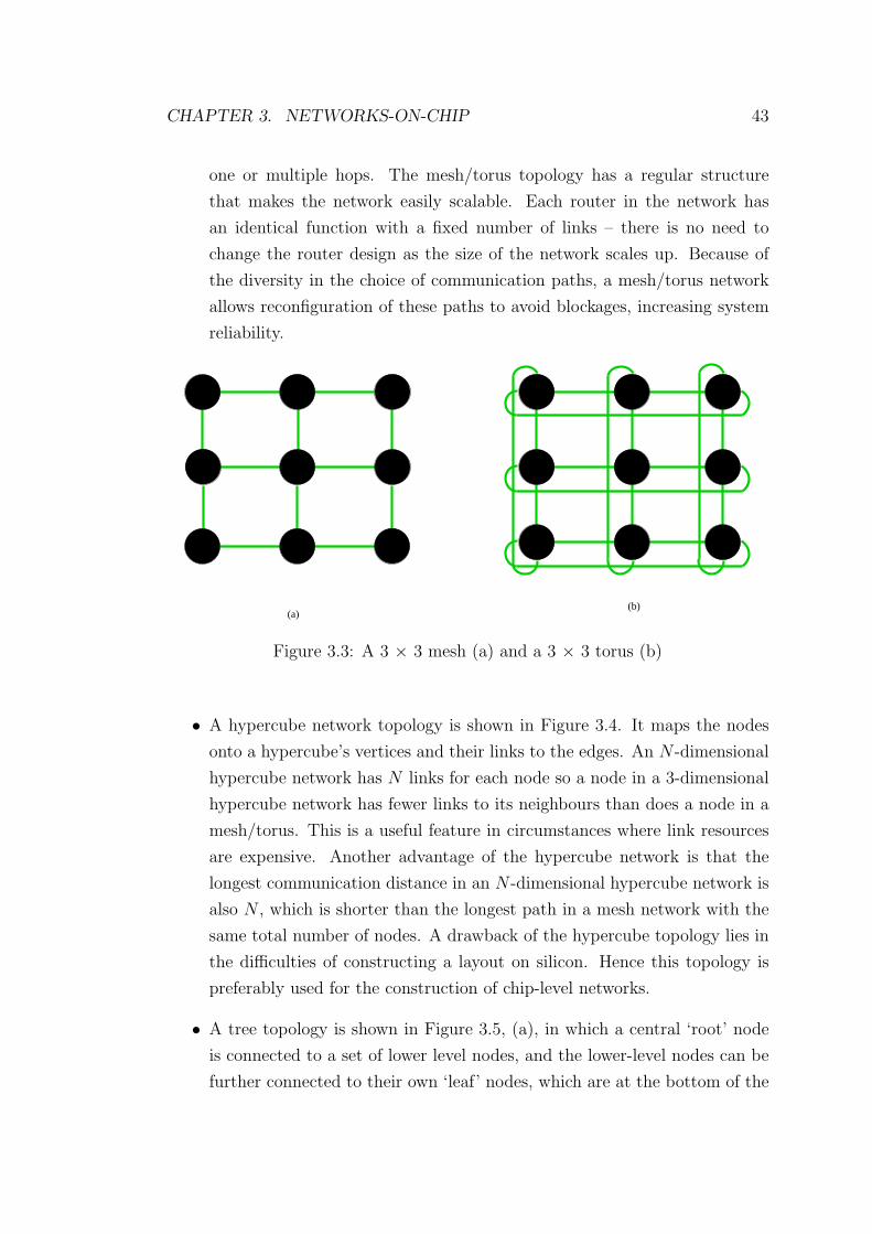
CHAPTER 3. NETWORKS-ON-CHIP 43
one or multiple hops. The mesh/torus topology has a regular structure
that makes the network easily scalable. Each router in the network has
an identical function with a fixed number of links – there is no need to
change the router design as the size of the network scales up. Because of
the diversity in the choice of communication paths, a mesh/torus network
allows reconfiguration of these paths to avoid blockages, increasing system
reliability.
(a)(b)
Figure 3.3: A 3 × 3 mesh (a) and a 3 × 3 torus (b)
• A hypercube network topology is shown in Figure 3.4. It maps the nodes
onto a hypercube’s vertices and their links to the edges. An N -dimensional
hypercube network has N links for each node so a node in a 3-dimensional
hypercube network has fewer links to its neighbours than does a node in a
mesh/torus. This is a useful feature in circumstances where link resources
are expensive. Another advantage of the hypercube network is that the
longest communication distance in an N -dimensional hypercube network is
also N , which is shorter than the longest path in a mesh network with the
same total number of nodes. A drawback of the hypercube topology lies in
the difficulties of constructing a layout on silicon. Hence this topology is
preferably used for the construction of chip-level networks.
• A tree topology is shown in Figure 3.5, (a), in which a central ‘root’ node
is connected to a set of lower level nodes, and the lower-level nodes can be
further connected to their own ‘leaf’ nodes, which are at the bottom of the
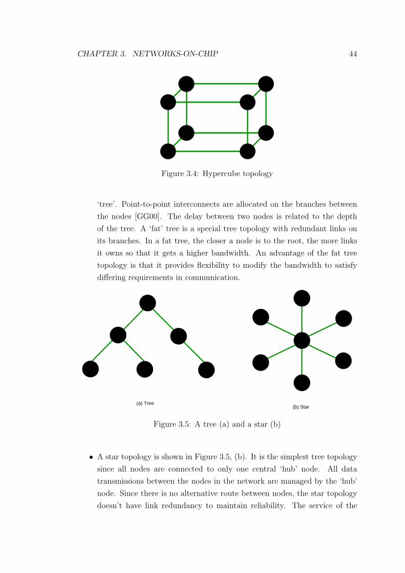
CHAPTER 3. NETWORKS-ON-CHIP 44
Figure 3.4: Hypercube topology
‘tree’. Point-to-point interconnects are allocated on the branches between
the nodes [GG00]. The delay between two nodes is related to the depth
of the tree. A ‘fat’ tree is a special tree topology with redundant links on
its branches. In a fat tree, the closer a node is to the root, the more links
it owns so that it gets a higher bandwidth. An advantage of the fat tree
topology is that it provides flexibility to modify the bandwidth to satisfy
differing requirements in communication.
(b) Star(a) Tree
Figure 3.5: A tree (a) and a star (b)
• A star topology is shown in Figure 3.5, (b). It is the simplest tree topology
since all nodes are connected to only one central ‘hub’ node. All data
transmissions between the nodes in the network are managed by the ‘hub’
node. Since there is no alternative route between nodes, the star topology
doesn’t have link redundancy to maintain reliability. The service of the

CHAPTER 3. NETWORKS-ON-CHIP 45
‘hub’ node is shared by all nodes, which requires arbitration in choosing
which node to send next. However, the star topology minimizes the number
of switches. This is important to reduce chip design cost. Moreover, it is
optimal for one-to-many communication since message transmissions from
any source to all destinations do not share any links. The star topology is a
special case of the tree topology where there is only one level of ‘leaf’ nodes.
Therefore, the star topology does not require redundant links to maintain
bandwidth for different levels of the nodes.
• The hierarchical topology is a hybrid structure formed with several layers.
An upper layer is a physical layer organizing groups of nodes in a lower layer.
A hierarchical topology network with different topologies combines their
benefits so that a better cost-performance trade-off is achieved. It is usually
applied to the construction of large-scale networks. The combination of
topologies may be chosen in accordance with specific routing requirements.
This thesis addresses the application of an NoC infrastructure to large-scale
neural simulation. The selection of the NoC topology should be made to enhance
the performance of this specific application. The benefits and the drawbacks of
different NoC topologies are summarized above. More discussion about the choice
of the NoC topology for a neural simulation platform will be addressed in chapter
4.
3.4 Router architecture and switching schemes
The communication of the interconnection network can be viewed as layered op-
erations, including the switching layer and the routing layer. The switching layer
uses switching schemes to select paths for messages passing through the network.
The routing layer uses routing algorithms to make routing decisions which deter-
mine the output channels at intermediate routers [DYN03]. This section and the
next section introduce these two layers and their respective categories. Ahead
of this, a generic router architecture will be introduced as the implementation of
the architecture is largely determined by these two layers.
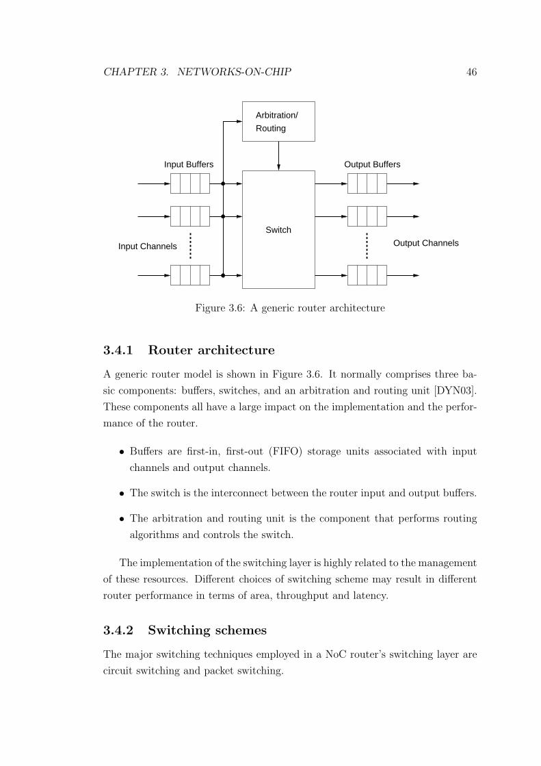
CHAPTER 3. NETWORKS-ON-CHIP 46
Input Buffers Output Buffers
Switch
Input Channels
Arbitration/
Routing
Output Channels
Figure 3.6: A generic router architecture
3.4.1 Router architecture
A generic router model is shown in Figure 3.6. It normally comprises three ba-
sic components: buffers, switches, and an arbitration and routing unit [DYN03].
These components all have a large impact on the implementation and the perfor-
mance of the router.
• Buffers are first-in, first-out (FIFO) storage units associated with input
channels and output channels.
• The switch is the interconnect between the router input and output buffers.
• The arbitration and routing unit is the component that performs routing
algorithms and controls the switch.
The implementation of the switching layer is highly related to the management
of these resources. Different choices of switching scheme may result in different
router performance in terms of area, throughput and latency.
3.4.2 Switching schemes
The major switching techniques employed in a NoC router’s switching layer are
circuit switching and packet switching.
CHAPTER 3. NETWORKS-ON-CHIP 47
• Circuit-switching: In this mode, a physical path is constructed for a mes-
sage before transfer. During transmission, routers and links are reserved
exclusively for the message until it reaches its destination; hence, the mes-
sage does not require to be arbitration and buffering at the intermediate
nodes. On the other hand, the reservation blocks other messages. The
hardware path is released after the complete message has been transmit-
ted. Because circuit switching minimizes propagation delay by eliminating
the intervening arbitration and buffering logic, it operates most efficiently
when messages are sparse and long.
• Packet-switching: In this mode, the message can be partitioned and sent
as fixed-length packets without prior path reservation. Because packet-
switching allows messages to share a link, the communication bandwidth
is utilized more efficiently than in circuit-switching. However, each packet
is individually arbitrated at each hop, and thus it needs to be buffered at
each intermediate node during the arbitration phase, introducing additional
delays. Therefore, the delay for packet-switching is unpredictable.
The majority of on-chip networks utilize packet-switching. They are typi-
cally categorized into three major kinds: store-and-forward switching, virtual
cut-through switching and wormhole switching. They differ in several respects.
• Store-and-forward switching: In this approach, an intermediate router must
store the complete packet in a buffer upon receiving it. The packet can only
be forwarded to the subsequent node if the output channel is available and
the receiving router has enough buffer space. Therefore, buffers require a
large capacity.
• Virtual cut-through switching: In this approach, a packet is forwarded with-
out waiting for the arrival of the entire packet. The path is determined based
on the reception of a portion of the packet, the packet header. If the buffer
at the next hop is available, the complete packet is forwarded by following
the header. Because only the header experiences routing delay, this tech-
nique reduces latency and requires smaller buffers than store-and-forward
routing. However, as virtual cut-through routing also allocates buffers at
packet-level, it occupies considerable buffer space especially if the packet
size is large [YLK08].
CHAPTER 3. NETWORKS-ON-CHIP 48
• Wormhole switching: In this approach, large message packets are handled
at flit-level. This is a special form of cut-through routing where a packet is
transmitted flit by flit. Because buffers in a wormhole router do not require
enough space to store the entire packet, smaller buffer sizes can be used
than in a virtual cut-through router. The packet is pipelined through the
network. When a network blockage occurs, rather than buffer a complete
packet as does virtual cut-through routing, wormhole routing may occupy
several segments of buffers along the network channels.
Clearly, if a NoC uses small packets, store-and-forward switching and virtual
cut-through switching are efficient, while if packets are big, wormhole switching
should be employed to optimize buffer and link utilization. Discussion of the
choice of switching technique for neural spike transmission will be addressed in
chapter 4.
3.5 Routing algorithms
Routing is the process of selecting paths for network traffic. It is performed by
routers, switches, or other similar devices. A routing algorithm is the protocol
that a router follows to make decisions on the path between a message’s source and
its destination. Proper selection of routing algorithms according to the specific
applications could significantly increase communication efficiency.
3.5.1 Source routing and distributed routing
Routing algorithms are classified into two basic categories: source routing and
distributed routing [CN99]. The performance of a NoC-based system is highly
dependent on the careful selection of routing algorithms.
In source routing, a routing decision is made on the basis of the information
carried by a packet throughout the routing process. The information contains an
entire path pre-defined at the source node. Because of this, intermediate nodes do
not need to make routing decisions [BMJ+98], and the source routing algorithm
cannot be performed in the absence of knowing a complete network topology.
In distributed routing, routing decisions are made by each node throughout a
packet’s journey. The routing algorithm is distributed across local nodes, each of
which performs packet switching only to either a local processor or a neighbouring
CHAPTER 3. NETWORKS-ON-CHIP 49
node. This is usually done through the management of a routing table which
specifies the outgoing route(s) according to the information forwarded from the
previous node [CSM94]. Because distributed routing does not require a node to
have complete routing information nor knowledge of the global network topology,
it allows the network topology be reconfigured through the modification of the
lookup tables. However, because the routing process is distributed across every
node, it is likely to introduce extra network latency for the routing decision and
extra storage for the routing table at each hop. These overheads have to be
considered for optimization in the design of an on-chip router.
3.5.2 Deterministic routing and adaptive routing
Routing algorithms are also classified as deterministic or adaptive. In determinis-
tic routing, the path between source and destination is predetermined and fixed.
Routing is adaptive if routing decisions are made depending on the dynamic
network status, thus allowing packets to select an escape path with freedom.
Deadlock is a situation that needs to be avoided in routing, it will be in-
troduced in the next section. A deterministic routing scheme can offer simple
guarantees of deadlock freedom and packet ordering, but may be bad at reduc-
ing network latency and increasing throughput because the network status is
dynamic. An adaptive routing scheme, on the other hand, can obtain a higher
throughput and a lower network latency, and tolerate component failures, al-
though they may have difficulty in maintaining packet ordering and may risk
causing deadlock if the algorithms are improperly designed [GGG+07][SK93].
As the traffic in neural simulations may be non-uniform and packet bursts may
happen occasionally, network congestion is likely to appear in a NoC implemen-
tation of neural networks. Because the ordering of the spike arrivals is not usually
of interest in neural network simulations, adaptive routing can be employed to
solve these problem. Some later chapters will show that a good adaptive routing
algorithm can significantly enhance the performance of NoC-based neural simu-
lations. They also show that a deadlock-free adaptive routing can be maintained
by selectively dropping deadlocked packets. This is because a certain data-loss
rate is usually tolerable in neurocomputing.
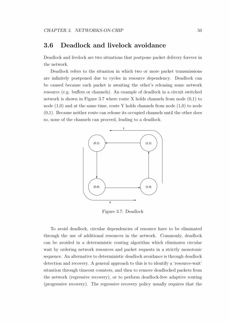
CHAPTER 3. NETWORKS-ON-CHIP 50
3.6 Deadlock and livelock avoidance
Deadlock and livelock are two situations that postpone packet delivery forever in
the network.
Deadlock refers to the situation in which two or more packet transmissions
are infinitely postponed due to cycles in resource dependency. Deadlock can
be caused because each packet is awaiting the other’s releasing some network
resource (e.g. buffers or channels). An example of deadlock in a circuit switched
network is shown in Figure 3.7 where route X holds channels from node (0,1) to
node (1,0) and at the same time, route Y holds channels from node (1,0) to node
(0,1). Because neither route can release its occupied channels until the other does
so, none of the channels can proceed, leading to a deadlock.
X
Y
(0,1)
(0,0)
(1,1)
(1,0)
Figure 3.7: Deadlock
To avoid deadlock, circular dependencies of resource have to be eliminated
through the use of additional resources in the network. Commonly, deadlock
can be avoided in a deterministic routing algorithm which eliminates circular
wait by ordering network resources and packet requests in a strictly monotonic
sequence. An alternative to deterministic deadlock avoidance is through deadlock
detection and recovery. A general approach to this is to identify a ‘resource-wait’
situation through timeout counters, and then to remove deadlocked packets from
the network (regressive recovery), or to perform deadlock-free adaptive routing
(progressive recovery). The regressive recovery policy usually requires that the
CHAPTER 3. NETWORKS-ON-CHIP 51
packets be recovered at the source and retransmitted.
Livelock is a situation where packets continue to move through network, but
never progress to the destination. Livelock can occur if non-minimal routing
is allowed, and it may cause too many mis-routes preventing the packet from
reaching its destination. A minimal routing algorithm always delivers a packet
through the shortest path where every channel the packet visits brings it closer to
the destination. A routing algorithm is non-minimal if the path is not guaranteed
to be minimal. Progressive deadlock recovery gives rise to non-minimal routing
and thus the risk of introducing livelock.
Livelock can be avoided by monitoring the states of packets, so called de-
terministic avoidance. The state can be a mis-route count that indicates how
many times a packet has been routed further from its destination (mis-routed),
or an age count that indicates for how many cycles a packet has travelled in the
network. If the state exceeds a threshold, the packet will be regarded as live-
locked and will be either discarded or re-issued. Livelock can also be avoided
by probabilistic avoidance that guarantees the probability of a packet’s routing
to its destination is always greater than 0. This is done by tracking the routing
history where the number of forward hops must be greater than the number of
backward hops. Probabilistic avoidance works in some real cases, but it is not
formally proved to prevent livelock.
3.7 Summary
This chapter discussed the benefits of NoCs, followed by their characteristics and
design methodologies for creating them. One of the key issues in designing an
NoC-based system, the communication scheme, was explicitly addressed. Sev-
eral sub-problems, including routing algorithms, network topologies, deadlock
and livelock, were considered. More details related to the implementation of a
NoC-based distributed system, SpiNNaker (a universal spiking neural network
simulator), will be presented in the next chapter. The system is a special and
practical application of multi-chip parallel computing. Based on the soundness of
applying neural simulations on to the system, the remainder of this dissertation
will further investigate the communication issues introduced in this chapter. As
a concrete example, the design of a sub-system of SpiNNaker, a communications
router, will be introduced.
Chapter 4
A NoC-based neurocomputing
platform
This chapter focuses on the system architecture and the communication schemes
for a multi-chip MPSoC system – SpiNNaker. The system is designed with the
primary application of emulating large neural systems using more ‘conventional’
computing elements. The system includes a large number of processors, each
independently modelling a number of neurons in real-time. There are particular
desired properties of communication and these have influenced the overall archi-
tecture. An asynchronous NoC is implemented on each chip and these extend
to external interfaces so that the network can be extended across the system.
A hardware router handles packet routing between processors and external in-
terfaces, including routing ‘through traffic’. As an MPSoC, the chip also needs
communication support for conventional system administration. This is done
by another asynchronous NoC. The router on each chip is programmable as a
peripheral device.
4.1 Introduction
The simulation of billions of neurons in real-time requires extremely high com-
munication efficiency. In biological neural networks, neurons interact with each
other via high density interconnections formed by synapses, dendrites, axons, etc.,
which communicate by carrying the neural spikes throughout the network. The
networks form very complex patterns of connectivity, and different patterns re-
sult in different network behaviours. A neural network processes incoming signals
52

CHAPTER 4. A NOC-BASED NEUROCOMPUTING PLATFORM 53
largely in accordance with its synaptic connectivity pattern [Get89]. Some neu-
ral computation models are highly related to the connection properties, e.g. ax-
onal delays [TDR01] and Spike-Timing Dependent Plasticity (STDP) [LKPD05],
which cannot be over simplified [FB09].
However, as was addressed in chapter 1, conventional communication schemes
on general-propose parallel computers and neurocomputers are inadequate to sup-
port the massive connectivity with efficiency. In VLSI systems, it is essential to
implement a connection structure, where many different patterns of connectiv-
ity can be accommodated. Therefore, a dedicated, programmable communica-
tion scheme is proposed for the SpiNNaker system. The proposed scheme has
to overcome three fundamental differences between biological systems and VLSI
hardware [Boa00]:
• The fan-ins and fan-outs of VLSI circuits are small – typically well below
ten, whereas those of neural network are in the thousands. For example, a
single presynaptic neuron in the vertebrate cortex is connected to up to 104
postsynaptic neurons [GK02].
• Most digital VLSI systems have central clocks to synchronize their signals.
However, there is no synchronizing clock in biological spiking neural net-
works. A presynaptic neuron imparts new information as a spike that occurs
asynchronously.
• Conventional buses in VLSI systems only support point-to-point or broad-
cast communication, whereas neural networks require one-to-many commu-
nication – a presynaptic neuron connects to many other neurons, but not
to every neuron in the system.
The complexity and density of interconnections in biological network make it
impractical to implement an equivalent level of physical interconnection in silicon
so instead virtual mapping of the connectivity using the homogeneous packet-
switching Communication NoC fabric is employed [FTB06]. Packet-switching on
the NoC is realised by a novel routing strategy using logical encoding of spikes
in an Address Event Representation (AER) packet format. This approach fully
decouples the hardware topology from the topology of the simulated network,
so the network is flexible enough to map different simulated network topologies
simply by re-programming the connectivity.
CHAPTER 4. A NOC-BASED NEUROCOMPUTING PLATFORM 54
4.2 Design issues
Chapters 1 to 3 presented literature reviews respectively on neural platforms,
neural models and NoC architectures. These form the basis of the design deci-
sions that were made during the development of the SpiNNaker system. More
specifically, the design decisions are listed below.
• Interconnect architecture selection: The literature review of neural plat-
forms in chapter 1 showed that conventional interconnect solutions are the
bottleneck to neural spike propagation. Therefore, a router-based NoC ar-
chitecture is chosen as the interconnect solution for SpiNNaker. This pro-
vides a much higher throughput for neural spike transmission and is flexible
for system scaling so that the system can support large-scale, real-time sim-
ulation.
• Neural model selection: The system has to exhibit flexibility to cope with
multiple neural models, the choice of model depending on its computa-
tional efficiency and simulation purposes. Chapter 2 discussed the three
generations of neural model where the third generation neural model, the
spiking neural model, is the more promising for large-scale, real-time sim-
ulation. Computationally-simple neural models are preferred because a
complex model, such as the Hodgkins-Huxley model, will not use the em-
bedded system’s resources efficiently. The models currently proposed for
support by the platform include the Izhikevich model [Izh03], which pro-
duces the rich spiking and bursting behaviour of cortical neurons, and the
PDP model [RM86], which is planned to be used to simulate the standard
features of normal reading. These different applications are expected to
have different interconnect patterns and produce neural messages which are
conveyed by small packets over the interconnect. The transmission of these
packets is handled by the router which is designed to be programmable so
that the interconnects can be configured.
• Network topology selection: Section 3.4 reviewed the basic topologies which
can be used in on-chip networks. The mesh topology is predominant in
state-of-the-art NoC designs because of its highly scalable and regular ar-
chitecture [YLK08]. However it is principally used for unicast services. It
provides a regular, reliable and easily scalable network. For neural spike
CHAPTER 4. A NOC-BASED NEUROCOMPUTING PLATFORM 55
transmission, multicast communication accounts for the majority of the
network traffic, and a mesh topology does not have sufficient connection
efficiency for this application. A star topology, on the other hand, is suit-
able for multicast communication where a packet is duplicated in the router
and sent to all destinations simultaneously. Hence, a hierarchical mesh-star
topology is efficient to support large-scale multicast services locally and is
good for scalability. The lower-layer star topology is suited to the situa-
tion where the construction cost for routers is high but that for channels
is low [MT99]. Therefore, the star topology is applied to the local on-chip
NoCs, where it is more important to minimize the on-chip switch count
to reduce the chip resource cost. In the mesh-star network, the multicast
service is localized to the lower-layer as much as possible, although the top-
layer mesh network should also support multicast routing. The top layer
mesh topology supports the construction of a chip array (Figure 4.2). Thus
the features of good reliability and scalability from the mesh topology are
maintained in the top-level network.
• Switching scheme selection: Based on the review of spiking neural networks
in chapter 2, a spike can be represented by the address of the neuron that
generated it, which is encoded as a small and independent packet when
transmitted by a router. The detailed representation of the spike will be
introduced in section 4.3.1. As a result of the characteristics of the packet
format, store-and-forward switching has been chosen as the switching tech-
nique for SpiNNaker. As discussed in section 3.4, there are three basic
packet switching schemes: store-and-forward, wormhole and virtual cut-
through switching. Although wormhole switching and virtual cut-through
switching decrease routing latency by handling flow-control at the flit-level,
they are not suitable for neural spike transmission because a routing deci-
sion has to be made on the basis of the entire neural packet. The store-
and-forward scheme is more suitable for SpiNNaker as it uses simpler logic
deriving faster routing decisions and higher throughput, as well as avoiding
flit-dependent deadlock. On the other hand, the buffer size is acceptable
since the neural packet is small.
Based on the above design decisions, the SpiNNaker interconnect system has
been determined. Its specifications will be introduced in the next section.
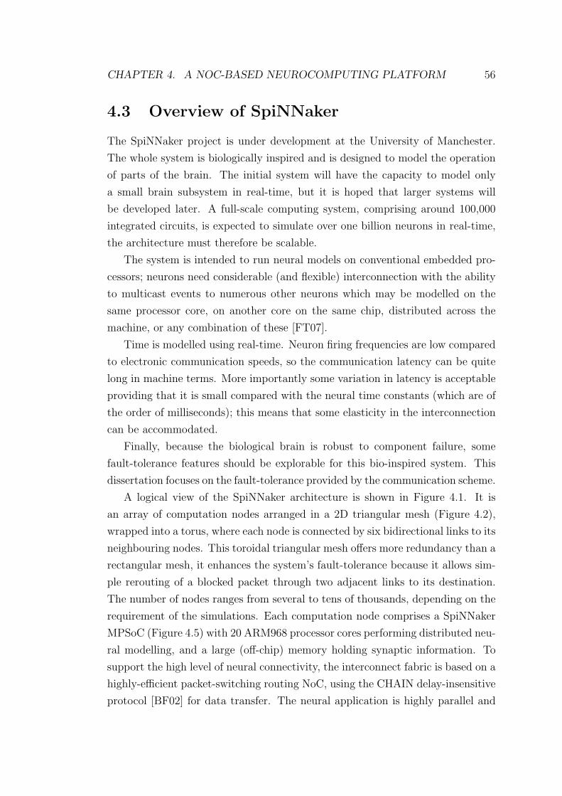
CHAPTER 4. A NOC-BASED NEUROCOMPUTING PLATFORM 56
4.3 Overview of SpiNNaker
The SpiNNaker project is under development at the University of Manchester.
The whole system is biologically inspired and is designed to model the operation
of parts of the brain. The initial system will have the capacity to model only
a small brain subsystem in real-time, but it is hoped that larger systems will
be developed later. A full-scale computing system, comprising around 100,000
integrated circuits, is expected to simulate over one billion neurons in real-time,
the architecture must therefore be scalable.
The system is intended to run neural models on conventional embedded pro-
cessors; neurons need considerable (and flexible) interconnection with the ability
to multicast events to numerous other neurons which may be modelled on the
same processor core, on another core on the same chip, distributed across the
machine, or any combination of these [FT07].
Time is modelled using real-time. Neuron firing frequencies are low compared
to electronic communication speeds, so the communication latency can be quite
long in machine terms. More importantly some variation in latency is acceptable
providing that it is small compared with the neural time constants (which are of
the order of milliseconds); this means that some elasticity in the interconnection
can be accommodated.
Finally, because the biological brain is robust to component failure, some
fault-tolerance features should be explorable for this bio-inspired system. This
dissertation focuses on the fault-tolerance provided by the communication scheme.
A logical view of the SpiNNaker architecture is shown in Figure 4.1. It is
an array of computation nodes arranged in a 2D triangular mesh (Figure 4.2),
wrapped into a torus, where each node is connected by six bidirectional links to its
neighbouring nodes. This toroidal triangular mesh offers more redundancy than a
rectangular mesh, it enhances the system’s fault-tolerance because it allows sim-
ple rerouting of a blocked packet through two adjacent links to its destination.
The number of nodes ranges from several to tens of thousands, depending on the
requirement of the simulations. Each computation node comprises a SpiNNaker
MPSoC (Figure 4.5) with 20 ARM968 processor cores performing distributed neu-
ral modelling, and a large (off-chip) memory holding synaptic information. To
support the high level of neural connectivity, the interconnect fabric is based on a
highly-efficient packet-switching routing NoC, using the CHAIN delay-insensitive
protocol [BF02] for data transfer. The neural application is highly parallel and
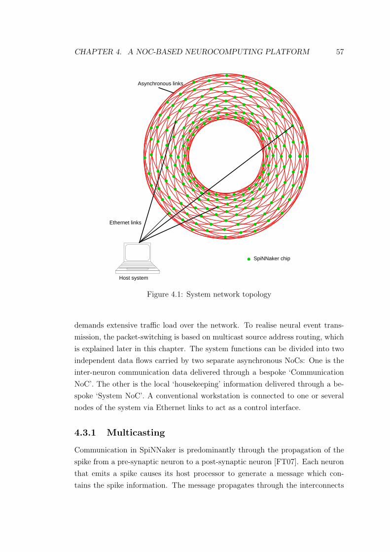
CHAPTER 4. A NOC-BASED NEUROCOMPUTING PLATFORM 57
SpiNNaker chip
Ethernet links
Asynchronous links
Host system
Figure 4.1: System network topology
demands extensive traffic load over the network. To realise neural event trans-
mission, the packet-switching is based on multicast source address routing, which
is explained later in this chapter. The system functions can be divided into two
independent data flows carried by two separate asynchronous NoCs: One is the
inter-neuron communication data delivered through a bespoke ‘Communication
NoC’. The other is the local ‘housekeeping’ information delivered through a be-
spoke ‘System NoC’. A conventional workstation is connected to one or several
nodes of the system via Ethernet links to act as a control interface.
4.3.1 Multicasting
Communication in SpiNNaker is predominantly through the propagation of the
spike from a pre-synaptic neuron to a post-synaptic neuron [FT07]. Each neuron
that emits a spike causes its host processor to generate a message which con-
tains the spike information. The message propagates through the interconnects
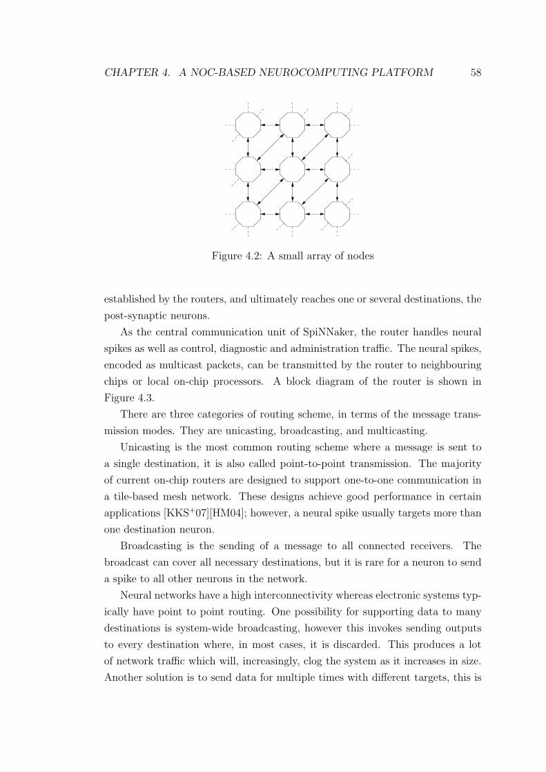
CHAPTER 4. A NOC-BASED NEUROCOMPUTING PLATFORM 58
Figure 4.2: A small array of nodes
established by the routers, and ultimately reaches one or several destinations, the
post-synaptic neurons.
As the central communication unit of SpiNNaker, the router handles neural
spikes as well as control, diagnostic and administration traffic. The neural spikes,
encoded as multicast packets, can be transmitted by the router to neighbouring
chips or local on-chip processors. A block diagram of the router is shown in
Figure 4.3.
There are three categories of routing scheme, in terms of the message trans-
mission modes. They are unicasting, broadcasting, and multicasting.
Unicasting is the most common routing scheme where a message is sent to
a single destination, it is also called point-to-point transmission. The majority
of current on-chip routers are designed to support one-to-one communication in
a tile-based mesh network. These designs achieve good performance in certain
applications [KKS+07][HM04]; however, a neural spike usually targets more than
one destination neuron.
Broadcasting is the sending of a message to all connected receivers. The
broadcast can cover all necessary destinations, but it is rare for a neuron to send
a spike to all other neurons in the network.
Neural networks have a high interconnectivity whereas electronic systems typ-
ically have point to point routing. One possibility for supporting data to many
destinations is system-wide broadcasting, however this invokes sending outputs
to every destination where, in most cases, it is discarded. This produces a lot
of network traffic which will, increasingly, clog the system as it increases in size.
Another solution is to send data for multiple times with different targets, this is
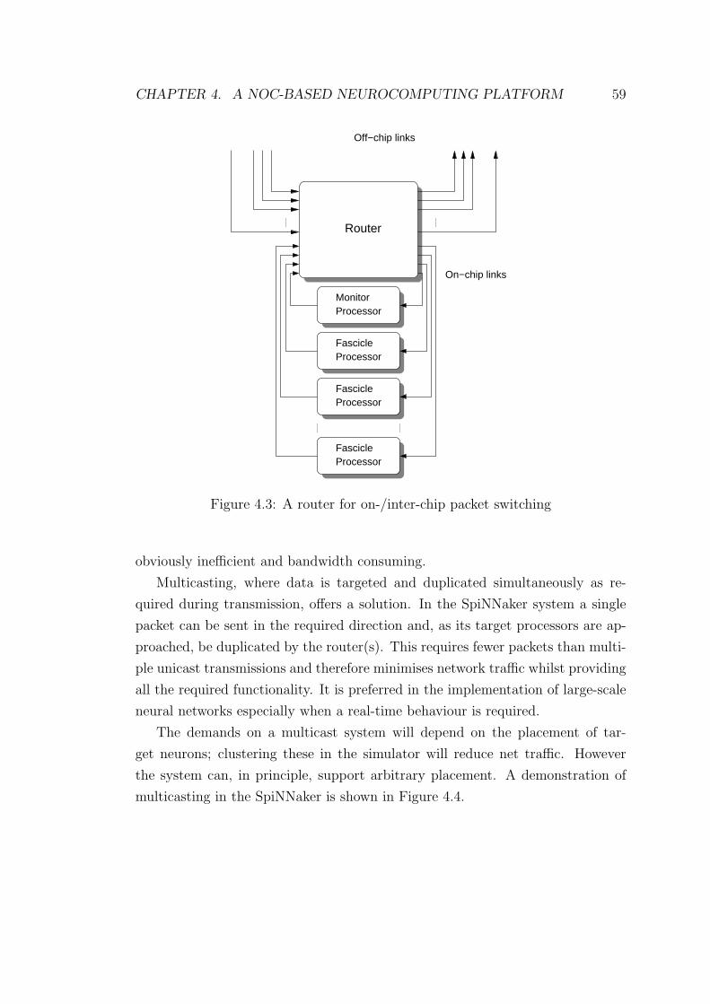
CHAPTER 4. A NOC-BASED NEUROCOMPUTING PLATFORM 59
Processor
Processor
Processor
Processor
Fascicle
Fascicle
Fascicle
Monitor
Off−chip links
On−chip links
Router
Figure 4.3: A router for on-/inter-chip packet switching
obviously inefficient and bandwidth consuming.
Multicasting, where data is targeted and duplicated simultaneously as re-
quired during transmission, offers a solution. In the SpiNNaker system a single
packet can be sent in the required direction and, as its target processors are ap-
proached, be duplicated by the router(s). This requires fewer packets than multi-
ple unicast transmissions and therefore minimises network traffic whilst providing
all the required functionality. It is preferred in the implementation of large-scale
neural networks especially when a real-time behaviour is required.
The demands on a multicast system will depend on the placement of tar-
get neurons; clustering these in the simulator will reduce net traffic. However
the system can, in principle, support arbitrary placement. A demonstration of
multicasting in the SpiNNaker is shown in Figure 4.4.
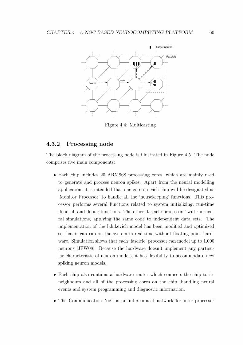
CHAPTER 4. A NOC-BASED NEUROCOMPUTING PLATFORM 60
−− Target neuron
Router
Source
Fascicle
Figure 4.4: Multicasting
4.3.2 Processing node
The block diagram of the processing node is illustrated in Figure 4.5. The node
comprises five main components:
• Each chip includes 20 ARM968 processing cores, which are mainly used
to generate and process neuron spikes. Apart from the neural modelling
application, it is intended that one core on each chip will be designated as
‘Monitor Processor’ to handle all the ‘housekeeping’ functions. This pro-
cessor performs several functions related to system initializing, run-time
flood-fill and debug functions. The other ‘fascicle processors’ will run neu-
ral simulations, applying the same code to independent data sets. The
implementation of the Izhikevich model has been modified and optimized
so that it can run on the system in real-time without floating-point hard-
ware. Simulation shows that each ‘fascicle’ processor can model up to 1,000
neurons [JFW08]. Because the hardware doesn’t implement any particu-
lar characteristic of neuron models, it has flexibility to accommodate new
spiking neuron models.
• Each chip also contains a hardware router which connects the chip to its
neighbours and all of the processing cores on the chip, handling neural
events and system programming and diagnostic information.
• The Communication NoC is an interconnect network for inter-processor
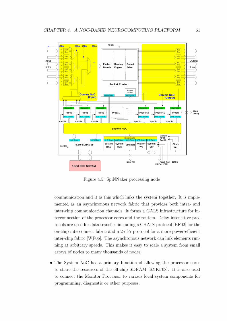
CHAPTER 4. A NOC-BASED NEUROCOMPUTING PLATFORM 61
2Gb/s
Comms NoC(Input) (Output)
Comms NoC
1Gb/s 8Gb/s4Gb/s
Proc3...
2of7Enc
2of7Dec
2of7Dec
2of7Dec
2of7Dec
2of7Dec
2of7Dec
2of7Enc
2of7Enc
2of7Enc
2of7Enc
2of7Enc
CpuClk CpuClk CpuClk CpuClk CpuClk CpuClk
Proc0 Proc1 Proc2 ProcN−1ProcN−2 ProcN
System NoC
MemClk
JTAGDebug
10MHz
Routercontrol
DecodePacket Routing Output
Engine Select
PL340 SDRAM I/F
TestPOR
ResetI/O Port
CtlrSystemWatch−
dogRAMSystem
ROMSystem Ethernet
Ether MII
1Gbit DDR SDRAM
Packet Router
AXI Master AXI MasterAXI MasterAXI MasterAXI MasterAXI Master
CommCtlr CommCtlrCommCtlr CommCtlr CommCtlrCommCtlr
Input
Links
Output
Links
RtrClk
PLLClock
MemClkRtrClkCpuClkAXI Slave APB Slave
AHB SlaveAHB Master
AHB SlaveAPB SlaveAHB Slave AHB Slave AHB SlaveSystem AHB
Figure 4.5: SpiNNaker processing node
communication and it is this which links the system together. It is imple-
mented as an asynchronous network fabric that provides both intra- and
inter-chip communication channels. It forms a GALS infrastructure for in-
terconnection of the processor cores and the routers. Delay-insensitive pro-
tocols are used for data transfer, including a CHAIN protocol [BF02] for the
on-chip interconnect fabric and a 2-of-7 protocol for a more power-efficient
inter-chip fabric [WF06]. The asynchronous network can link elements run-
ning at arbitrary speeds. This makes it easy to scale a system from small
arrays of nodes to many thousands of nodes.
• The System NoC has a primary function of allowing the processor cores
to share the resources of the off-chip SDRAM [RYKF08]. It is also used
to connect the Monitor Processor to various local system components for
programming, diagnostic or other purposes.
CHAPTER 4. A NOC-BASED NEUROCOMPUTING PLATFORM 62
• The synaptic weights that couple the spike to its postsynaptic neurons are
stored in an off-chip SDRAM with 1Gb storage, and are processed by the
receiving processor. The weights can be updated to perform a learning
algorithm. Unlike some previous neural chips that implement neural com-
munication delays in hardware, the SpiNNaker chip models these delays
in local processing nodes in software to achieve flexibility. These neuron
propagation delays are stored in the SDRAM.
The router, the Communication NoC and the System NoC are the three main
components of the communication infrastructure in the SpiNNaker.
4.3.3 Fault-tolerance
The cost of verification of SoCs is increasing rapidly, and the probability of deep
submicron (DSM) failures is getting higher due to cross-talk noise, electromag-
netic interference, etc [DM03]. Conventional computing systems require absolute
reliability of on-chip interconnects and processing elements. Biological neural net-
works, on the other hand, exhibit considerable robustness in the presence of small
lesions: neurons die continuously yet brains (largely) continue to function. This
system level fault-tolerance can potentially overcome hardware failure in DSM
systems and consequently reduce the design costs. To achieve fault-tolerance, an
NoC must have enough redundancy to be able to support run-time reconfiguration
when part of the network is congested because of either a transient or permanent
failure. In certain applications, such as neural network simulations and multime-
dia processing, it is considered inessential that every event is communicated to all
its targets. A best-effort approach may involve discarding a proportion of signals
to allow the majority to arrive relatively unimpeded. There is also a possibility
– a near certainty as the system scale expands – that some processing elements
may fail either temporarily due to overloading or permanently due to hardware
faults. It is intended that the system should try to tolerate faults at this level
too.
4.4 Event-driven communication
Message transmissions of neural simulation on a VLSI system can be realized
using event-driven communication [RCO+06]. Spiking neurons interact with each
CHAPTER 4. A NOC-BASED NEUROCOMPUTING PLATFORM 63
other by emitting spikes asynchronously. It is the arrival of a spike that carries
the information not the magnitude or the shape. These spikes can be treated as
a sequence of events driving information processing in a neural network.
4.4.1 Address event representation
In a spiking neural network, a neuron firing is a purely asynchronous event which
carries no information other than that it has occurred. The occurrence, timing
and frequency of firing appears to convey the desired information. This makes the
communication scheme an event-driven one, where the communication packets
can be short, typically carrying nothing but the identity of their source. Prac-
tically, this means that some ‘address’ information may be needed and the data
payload is minimal.
Address event representation (AER) is a protocol, specifically supporting
event-driven communications [Sil02][Siv91][Mah92]. It is used in spiking neu-
ral modelling where a set of processing elements compute events simultaneously
and receive/send events asynchronously. Each element in the system has a unique
address that represents events issued by that element. If the event consists of a
target element address, it is called a target address event. If the event consists
of a source element address, it is called a source address event.
Each neuron in a spiking neural network is identified as a processing element
with its own address, hence, the information carried by an event packet can be
encoded as the neuron’s address and its time of issue. As, in electronic terms,
neural events are widely separated in time they can be conveyed ‘instantaneously’
and time then models itself, removing the need for time-stamping packets. Spike
transmission is based on the routing of the packets according to their addresses.
The packet size can be very small, but represents a very large group of neu-
rons. Consider a neural network with N neurons in total, each neuron requires
log2 N bits for address encoding. A 32-bit wide address, for example, is able to
represent up to about 4 billion (232) neurons. Because of the smaller packet size,
communication efficiency is significantly improved.
In a parallel neural simulator with multiple processing nodes, a neural event
packet’s address space can be defined by the combination of a node address and a
relative address of a subset of neurons bundled in the node (fascicle) [Sil02]. The
node address is the common address of the subset of neurons. Each neuron in a
node has a relative address which is only visible locally. The complete address
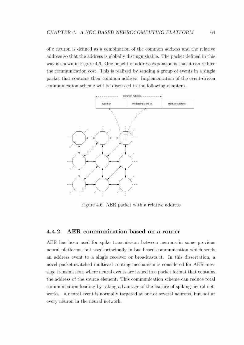
CHAPTER 4. A NOC-BASED NEUROCOMPUTING PLATFORM 64
of a neuron is defined as a combination of the common address and the relative
address so that the address is globally distinguishable. The packet defined in this
way is shown in Figure 4.6. One benefit of address expansion is that it can reduce
the communication cost. This is realized by sending a group of events in a single
packet that contains their common address. Implementation of the event-driven
communication scheme will be discussed in the following chapters.
Node ID Relative AddressProcessing Core ID
Common Address
Figure 4.6: AER packet with a relative address
4.4.2 AER communication based on a router
AER has been used for spike transmission between neurons in some previous
neural platforms, but used principally in bus-based communication which sends
an address event to a single receiver or broadcasts it. In this dissertation, a
novel packet-switched multicast routing mechanism is considered for AER mes-
sage transmission, where neural events are issued in a packet format that contains
the address of the source element. This communication scheme can reduce total
communication loading by taking advantage of the feature of spiking neural net-
works – a neural event is normally targeted at one or several neurons, but not at
every neuron in the neural network.
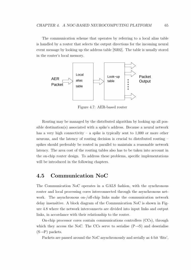
CHAPTER 4. A NOC-BASED NEUROCOMPUTING PLATFORM 65
The communication scheme that operates by referring to a local alias table
is handled by a router that selects the output directions for the incoming neural
event message by looking up the address table [Sil02]. The table is usually stored
in the router’s local memory.
Packet Look−uptable
Packet
AEROutputalias
Local
table
Figure 4.7: AER-based router
Routing may be managed by the distributed algorithm by looking up all pos-
sible destination(s) associated with a spike’s address. Because a neural network
has a very high connectivity – a spike is typically sent to 1,000 or more other
neurons, and the latency of routing decision is crucial to distributed routing –
spikes should preferably be routed in parallel to maintain a reasonable network
latency. The area cost of the routing tables also has to be taken into account in
the on-chip router design. To address these problems, specific implementations
will be introduced in the following chapters.
4.5 Communication NoC
The Communication NoC operates in a GALS fashion, with the synchronous
router and local processing cores interconnected through the asynchronous net-
work. The asynchronous on-/off-chip links make the communication network
delay insensitive. A block diagram of the Communication NoC is shown in Fig-
ure 4.8 where the network interconnects are divided into input links and output
links, in accordance with their relationship to the router.
On-chip processor cores contain communications controllers (CCs), through
which they access the NoC. The CCs serve to serialise (P→S) and deserialise
(S→P) packets.
Packets are passed around the NoC asynchronously and serially as 4-bit ‘flits’,
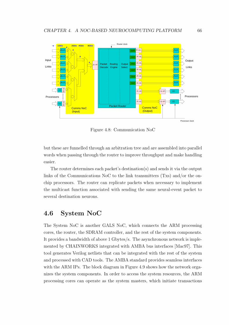
CHAPTER 4. A NOC-BASED NEUROCOMPUTING PLATFORM 66
2Gb/s 4Gb/s1Gb/s
(Input)
8Gb/s
Comms NoC Comms NoC(Output)
DecodePacket
Engine SelectRouting Output
BUF
BUF
BUF
BUF
BUF
P−>S
P−>S
Links
Router clock
Output
Links
Processor clock
Processors Processors
Packet Router
P−>S
P−>S
P−>S
Input
BUF P−>S
P−
>S
P−
>S
S−>P
Rx i/f
Rx i/f
Rx i/f
Rx i/f
Rx i/f
Rx i/f
CC
CC
CC
CC
Tx i/f
Tx i/f
Tx i/f
Tx i/f
Tx i/f
Tx i/f
S−>PP−>S
P−>S S−>P
Figure 4.8: Communication NoC
but these are funnelled through an arbitration tree and are assembled into parallel
words when passing through the router to improve throughput and make handling
easier.
The router determines each packet’s destination(s) and sends it via the output
links of the Communications NoC to the link transmitters (Txs) and/or the on-
chip processors. The router can replicate packets when necessary to implement
the multicast function associated with sending the same neural-event packet to
several destination neurons.
4.6 System NoC
The System NoC is another GALS NoC, which connects the ARM processing
cores, the router, the SDRAM controller, and the rest of the system components.
It provides a bandwidth of above 1 Gbytes/s. The asynchronous network is imple-
mented by CHAINWORKS integrated with AMBA bus interfaces [Mac97]. This
tool generates Verilog netlists that can be integrated with the rest of the system
and processed with CAD tools. The AMBA standard provides seamless interfaces
with the ARM IPs. The block diagram in Figure 4.9 shows how the network orga-
nizes the system components. In order to access the system resources, the ARM
processing cores can operate as the system masters, which initiate transactions
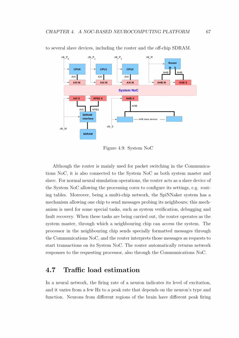
CHAPTER 4. A NOC-BASED NEUROCOMPUTING PLATFORM 67
to several slave devices, including the router and the off-chip SDRAM.
0 1 2
CPU0 CPU1 CPU2
AXI M AXI M
AXI S APB3 S AHB S
AHB MAXI M
APB3
SM
Router
clk_P clk_P clk_R
AHB S
AHB
clk_M
clk_P
AHBAXI
interfaceSDRAM
SDRAM
AHB slave devices
clk_S
AXIAXIAXI
AHB
System NoC
Figure 4.9: System NoC
Although the router is mainly used for packet switching in the Communica-
tions NoC, it is also connected to the System NoC as both system master and
slave. For normal neural simulation operations, the router acts as a slave device of
the System NoC allowing the processing cores to configure its settings, e.g. rout-
ing tables. Moreover, being a multi-chip network, the SpiNNaker system has a
mechanism allowing one chip to send messages probing its neighbours; this mech-
anism is used for some special tasks, such as system verification, debugging and
fault recovery. When these tasks are being carried out, the router operates as the
system master, through which a neighbouring chip can access the system. The
processor in the neighbouring chip sends specially formatted messages through
the Communications NoC, and the router interprets those messages as requests to
start transactions on its System NoC. The router automatically returns network
responses to the requesting processor, also through the Communications NoC.
4.7 Traffic load estimation
In a neural network, the firing rate of a neuron indicates its level of excitation,
and it varies from a few Hz to a peak rate that depends on the neuron’s type and
function. Neurons from different regions of the brain have different peak firing

CHAPTER 4. A NOC-BASED NEUROCOMPUTING PLATFORM 68
rates, for example, the typical peak firing rates of cortical neurons is around
100 Hz. Some other types of neuron can fire at rates up to 1000 Hz; this is the
maximum firing rate of any biological neuron. The traffic in a neural network
is therefore non-uniform, and high-frequency bursts of spikes may happen from
time-to-time. The router needs to ensure that the system is capable of running
simulations in real-time, it is thus designed to maintain the bandwidth required to
handle high-frequency packet bursts. The design trade-off between performance
and power also has to be considered because a high bandwidth is usually achieved
by means of a wide bus and/or a high clock frequency, which can imply high
power consumption. Therefore, the maximum traffic load of the router must be
estimated.
As the operating speed of the neurons is low, a CC gives a low throughput
– e.g. for an average of a 1000 Hz spike rate on each neuron and each fascicle
processor can model up to 1000 neurons, the total throughput from the processor’s
links is:
1000 neurons/processor × 1000 packet/(neurons · s) = 1M spikes/s (4.1)
As mentioned before, a 32-bit neuron identifier is capable of simulating up to
∼4 billion (232) neurons. Hence, the packet has a size of 40 bits (32-bit neuron
address and 8-bit header) and its detailed definition will be introduced in the
next chapter. The throughput of the processor’s link then equals to 40Mbps
(1M spikes × 40 bits/spike).
For a SpiNNaker chip with 20 fascicle processors, 19 are used for neuron
modelling. The on-chip traffic load gives:
19× 1M spikes/s = 19M spikes/s (4.2)
The on-chip link is implemented by CHAINWORKS, a commercial tool that
generates the self-timed on-chip interconnect [BF02]. A single CHAIN link pro-
vides a bandwidth of about 2 Gbps. Thus the processor links merge through a
single-link arbiter tree.
This represents the maximum data rate generated by the chip. In addition
each of the 6 inter-chip links can carry up to around 1 Gb/s bandwidth [WF06],
so the overall peak traffic load on chip is:
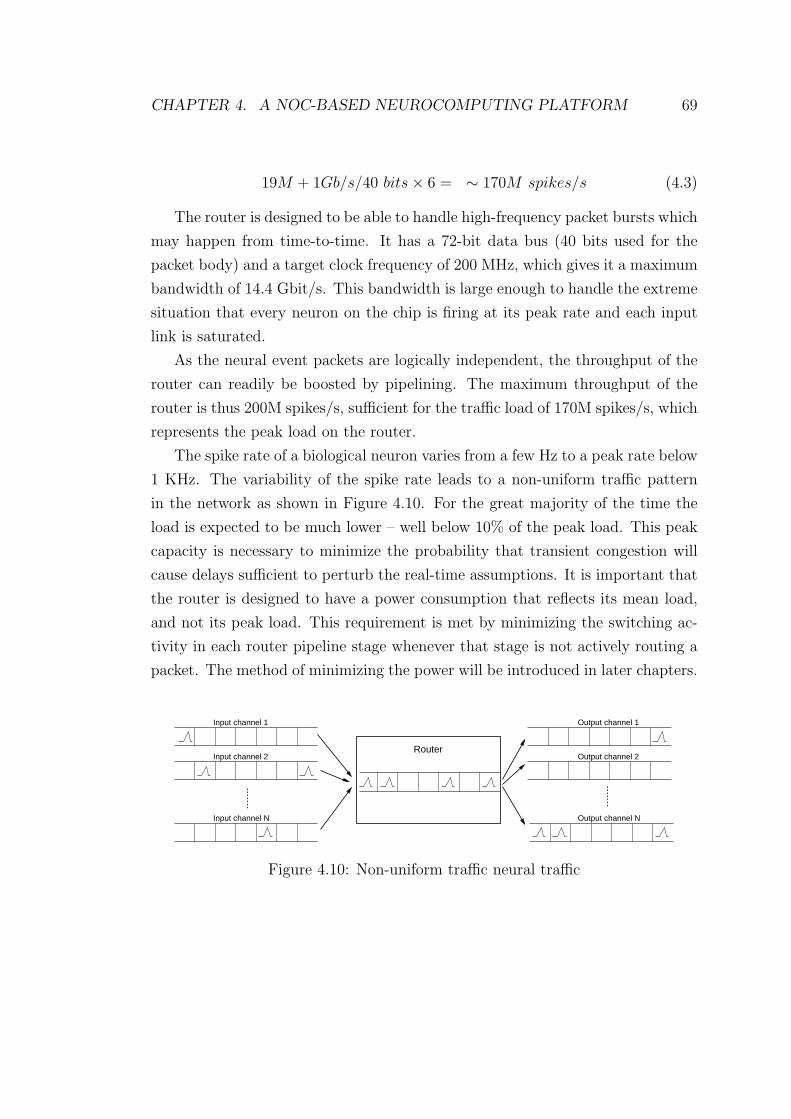
CHAPTER 4. A NOC-BASED NEUROCOMPUTING PLATFORM 69
19M + 1Gb/s/40 bits× 6 = ∼ 170M spikes/s (4.3)
The router is designed to be able to handle high-frequency packet bursts which
may happen from time-to-time. It has a 72-bit data bus (40 bits used for the
packet body) and a target clock frequency of 200 MHz, which gives it a maximum
bandwidth of 14.4 Gbit/s. This bandwidth is large enough to handle the extreme
situation that every neuron on the chip is firing at its peak rate and each input
link is saturated.
As the neural event packets are logically independent, the throughput of the
router can readily be boosted by pipelining. The maximum throughput of the
router is thus 200M spikes/s, sufficient for the traffic load of 170M spikes/s, which
represents the peak load on the router.
The spike rate of a biological neuron varies from a few Hz to a peak rate below
1 KHz. The variability of the spike rate leads to a non-uniform traffic pattern
in the network as shown in Figure 4.10. For the great majority of the time the
load is expected to be much lower – well below 10% of the peak load. This peak
capacity is necessary to minimize the probability that transient congestion will
cause delays sufficient to perturb the real-time assumptions. It is important that
the router is designed to have a power consumption that reflects its mean load,
and not its peak load. This requirement is met by minimizing the switching ac-
tivity in each router pipeline stage whenever that stage is not actively routing a
packet. The method of minimizing the power will be introduced in later chapters.
RouterInput channel 2
Input channel 1
Input channel N
Output channel 2
Output channel N
Output channel 1
Figure 4.10: Non-uniform traffic neural traffic
CHAPTER 4. A NOC-BASED NEUROCOMPUTING PLATFORM 70
4.8 Summary
This chapter focused on the communication issues of a neural application-specific
system – SpiNNaker. Firstly, the system architecture was introduced. A router
that supports multicast routing was then proposed to offer an effective solution
of minimising traffic in neural networks. An AER protocol is employed for neural
event routing, thus provides a large address space capable of handling billions
of neurons. Unlike conventional implementations of the AER protocol, which
uses a bus, SpiNNaker uses packet-switched routing to enhance communication
efficiency. The system contains two GALS style networks, the Communication
NoC and the System NoC. The two NoCs are both connected to the router which
conveys neural event packets as well as system information. The router’s traffic
load was estimated to ensure that the router is able to fulfill the communication
requirement. The next chapter focuses on the design of the SpiNNaker router.
Chapter 5
A router in a neural platform
The previous chapter introduced the SpiNNaker neural platform’s system archi-
tecture and its communication infrastructure. This chapter focuses principally
on the SpiNNaker router, which is a key component of this application-specific
multi-core system. In order to support the many features of the platform, the
router performs multiple routing algorithms concurrently. The router is designed
specifically to fulfill the requirement of real-time neural communications and,
unlike most on-chip one-to-one interconnect, it supports multicast routing of
neural event packets. As well as running its neural applications the system is,
in one sense, a ‘conventional’ computer and will need some ‘housekeeping’ fea-
tures. These include the ability to load and alter the neural models, which means
programming the processor cores and the interconnect. There is also a require-
ment for debugging which may be used both to commission the system and as a
run-time feature to enhance fault tolerance. These last features have also been
designed into the router although, perhaps fortunately, they are absent in the
brain!
5.1 Introduction
Modern VLSI systems are able to operate at approximately 10 GHz maximum,
while biological neurons’ maximum firing rate is ∼1000 Hz. The parallel mod-
elling of many neurons in real-time can be achieved by taking advantage of the
computational power of a single processor where the number of neurons in the
simulation will be largely determined by the clock rate of the processor. For ex-
ample, if a neural network is modelled on a processor which operates at 10 GHz
71
CHAPTER 5. A ROUTER IN A NEURAL PLATFORM 72
and finishes processing a neural spike in one clock cycle, its maximum processing
ability is 10 M (10 GHz / 1000 Hz) neurons. A more realistic number is 1M neu-
rons per processor, which is achieved in MASPINN [SMJK98]. Unfortunately,
1 M (or 10 M) is still a small number compared to those in biological neural
systems. To overcome the neuron population boundary, computation has to be
distributed to multiple processors.
Many different platforms for parallel neural simulation were reviewed in chap-
ter 1. Some of those are capable of simulating more than 10 M neurons but
much slower than real-time [SMJK98]. It was recognized that the communica-
tion overhead was the bottleneck to the speed, and there are two conventional
solutions for inter-processor spike propagation. General-purpose cluster comput-
ers use computer networks with stand-alone routers, which are not designed for
optimal neural message transmission. Neuroaccelerators use dedicated architec-
tures which commonly comprise a neuron computation unit, a connection unit
and spike event list. Prototype can be found in SPIKE128K, NESPINN and
MASPINN. The neuron computation unit first generates neural spikes, whose
addresses are stored in the spike list; communication between neurons is then
established by the connection unit, which supplies target neuron address accord-
ing to the source neuron address obtained from the spike event list. Operations
of these three elements all require memory access, whose bandwidth maybe the
bottleneck of the system; such a system is non-scalable.
In this thesis, a novel NoC concept is proposed to accelerate communication.
Its communication ability can fulfill the requirement of massive spike transmission
rate in parallel neural simulations. As the central element of the NoC, the router
should be carefully designed to ensure the real-time performance of the system.
5.2 Routing requirements
The router is designed to operate in a GALS environment – it connects to two
asynchronous NoCs, whilst the router itself is implemented in a synchronous style
to take advantage of standard VLSI design flows, and to ease the integration of
third-party clocked blocks, such as memories. The router has a target clock fre-
quency of 200 MHz. Thanks to the GALS implementation of the chip, the clock
frequency is decoupled from other system clocks by the asynchronous intercon-
nect, therefore the router’s clock can be adjusted to be lower or higher than
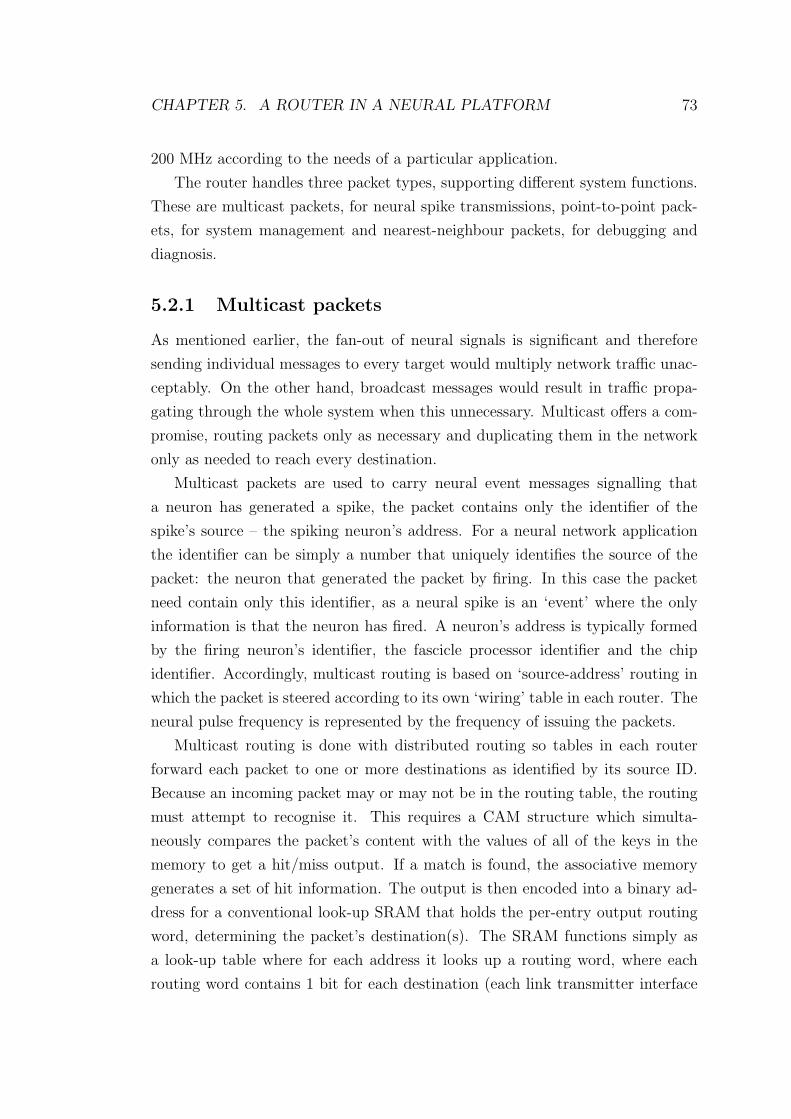
CHAPTER 5. A ROUTER IN A NEURAL PLATFORM 73
200 MHz according to the needs of a particular application.
The router handles three packet types, supporting different system functions.
These are multicast packets, for neural spike transmissions, point-to-point pack-
ets, for system management and nearest-neighbour packets, for debugging and
diagnosis.
5.2.1 Multicast packets
As mentioned earlier, the fan-out of neural signals is significant and therefore
sending individual messages to every target would multiply network traffic unac-
ceptably. On the other hand, broadcast messages would result in traffic propa-
gating through the whole system when this unnecessary. Multicast offers a com-
promise, routing packets only as necessary and duplicating them in the network
only as needed to reach every destination.
Multicast packets are used to carry neural event messages signalling that
a neuron has generated a spike, the packet contains only the identifier of the
spike’s source – the spiking neuron’s address. For a neural network application
the identifier can be simply a number that uniquely identifies the source of the
packet: the neuron that generated the packet by firing. In this case the packet
need contain only this identifier, as a neural spike is an ‘event’ where the only
information is that the neuron has fired. A neuron’s address is typically formed
by the firing neuron’s identifier, the fascicle processor identifier and the chip
identifier. Accordingly, multicast routing is based on ‘source-address’ routing in
which the packet is steered according to its own ‘wiring’ table in each router. The
neural pulse frequency is represented by the frequency of issuing the packets.
Multicast routing is done with distributed routing so tables in each router
forward each packet to one or more destinations as identified by its source ID.
Because an incoming packet may or may not be in the routing table, the routing
must attempt to recognise it. This requires a CAM structure which simulta-
neously compares the packet’s content with the values of all of the keys in the
memory to get a hit/miss output. If a match is found, the associative memory
generates a set of hit information. The output is then encoded into a binary ad-
dress for a conventional look-up SRAM that holds the per-entry output routing
word, determining the packet’s destination(s). The SRAM functions simply as
a look-up table where for each address it looks up a routing word, where each
routing word contains 1 bit for each destination (each link transmitter interface
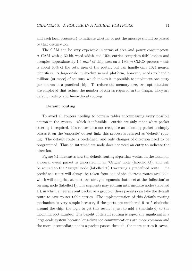
CHAPTER 5. A ROUTER IN A NEURAL PLATFORM 74
and each local processor) to indicate whether or not the message should be passed
to that destination.
The CAM can be very expensive in terms of area and power consumption.
A CAM with a 32-bit word-width and 1024 entries comprises 64K latches and
occupies approximately 1.6 mm2 of chip area on a 130nm CMOS process – this
is about 60% of the total area of the router, but can handle only 1024 neuron
identifiers. A large-scale multi-chip neural platform, however, needs to handle
millions (or more) of neurons, which makes it impossible to implement one entry
per neuron in a practical chip. To reduce the memory size, two optimizations
are employed that reduce the number of entries required in the design. They are
default routing and hierarchical routing.
Default routing
To avoid all routers needing to contain tables encompassing every possible
neuron in the system – which is infeasible – entries are only made when packet
steering is required. If a router does not recognise an incoming packet it simply
passes it on the ‘opposite’ output link; this process is referred as ‘default’ rout-
ing. The default route is predefined, and only changes of direction need to be
programmed. Thus an intermediate node does not need an entry to indicate the
direction.
Figure 5.1 illustrates how the default routing algorithm works. In the example,
a neural event packet is generated in an ‘Origin’ node (labelled O), and will
be routed to the ‘Target’ node (labelled T) traversing a predefined route. The
predefined route will always be taken from one of the shortest routes available,
which will comprise, at most, two straight segments that meet at the ‘Inflection’ or
turning node (labelled I). The segments may contain intermediate nodes (labelled
D), in which a neural event packet or a group of those packets can take the default
route to save router table entries. The implementation of this default routing
mechanism is very simple because, if the ports are numbered 0 to 5 clockwise
around the chip, the logic to get this result is just to add 3 (modulo 6) to the
incoming port number. The benefit of default routing is especially significant in a
large-scale system because long-distance communications are more common and
the more intermediate nodes a packet passes through, the more entries it saves.
CHAPTER 5. A ROUTER IN A NEURAL PLATFORM 75
O
D
D TI
Figure 5.1: Default routing
Hierarchical routing
Another optimization to further reduce the routing table exploits the obser-
vation that each fascicle processor can be used to model groups of neurons (‘fas-
cicles’) that have associated inputs and outputs, so that neurons in each group
share the same destinations and can be hierarchically routed by a single routing
entry [DT03].
In a neural network, neighbouring biological neurons usually have associated
inputs and outputs. This feature can be used to cluster neurons on a processor so
that the router only needs to know the group’s destination, or to cluster processors
on the same chip so that only that chip’s router needs to know the routing
information. Packets are then routed in groups.
After neurons have been grouped, each group makes some of its identifier bits,
which have no relevance in determining a packet’s destination, ‘don’t care’ as far
as the look-up process is concerned. Hierarchical routing is accomplished by se-
lectively ignoring these ‘don’t care’ bits. Figure 5.2 shows the CAM’s comparison
mechanism which marks the bits as ‘don’t care’ when the identifier is under a
mask.
Thus a particular entry [i ] will match only if:
• wherever a bit in the mask[i ] word is ‘1’, the corresponding bit in the

CHAPTER 5. A ROUTER IN A NEURAL PLATFORM 76
multicast (MC) packet routing word is the same as the corresponding bit
in the key[i ] word, AND
• wherever a bit in the mask[i ] word is ‘0’, the corresponding bit in the key[i ]
word is also ‘0’.
routing key
key data mask data
32
line hit
hit/miss
hitaddress
32
32
EN
CO
DE
RP
RIO
RIT
Y
Figure 5.2: Masked associative memory logic
Hierarchical routing largely reduces the number of routing entries. For exam-
ple in Figure 5.3, for a chip with a fascicle size of 256 neurons, the number of
entries can be reduced from 20K (Equation 5.1) to 80 (Equation 5.2) by masking
8 bits of the neuron identifier, resulting in a big saving of chip area.
1 1 1 1 1 1 1 1 10 0 0 0 0 0 0 0 0 0 0 0 0 01
1 1 1 1 1 10 0 0 0 0 0 0 0 0 0 x x x x x x xx
1 1 1 1 1 1 0000000011 1 1 1 1 1 1 1 1
AND
Chip ID
Routing key
Mask
Masked key
Processor ID
Lookup table
Neuron ID
Figure 5.3: Multicast routing with mask
CHAPTER 5. A ROUTER IN A NEURAL PLATFORM 77
Each packet routed independently:
1024× 20 = 20K entries/chip (5.1)
256 packets routed in groups:
(1024/256)× 20 = 80 entries/chip (5.2)
5.2.2 Point-to-point packets
Besides the neural simulation function, SpiNNaker also needs communication
support for conventional system management. As an experimental platform, the
system may need to transfer some monitoring information back to the Host. These
are carried between the Host and the ‘Monitor’ Processor cores by point-to-point
(P2P) packets.
Steering point-to-point packets is unicast routing. This could be determined
algorithmically as the current and final positions are known; however, because the
P2P packets are transferred at chip level, a P2P routing table is small enough to be
accommodated on a chip. Therefore the point-to-point router is a straightforward
look-up, implemented using an SRAM. The packet has a 16-bit destination ID
which is used as the look-up address of the SRAM.
5.2.3 Nearest-neighbour packets
Nearest-neighbour (NN) packets communicate amongst only the nearest neigh-
bour chips. They are used for run-time ‘flood-fill’ system loading and also for
neighbouring nodes to access the local System NoC resources for debugging and
fault recovery. Nearest-neighbour packets are routed algorithmically. When a
nearest-neighbour packet is determined to have reached its destination it is routed
to the core currently designated as ‘Monitor’ Processor. There are two different
forms of these packets.
The ‘normal’ form of NN packets are used for ‘flood-fill’ – a procedure of
loading data from the Host PC into each node of the network prior to the system
starting-up. Data may include the neural modelling run-time program, neural
network connectivity information, and synaptic weights. The data, initially issued
by the Host System, is first sent to one or several chips which have a direct physical
connection to the Host System. These chips then broadcast the data to all their
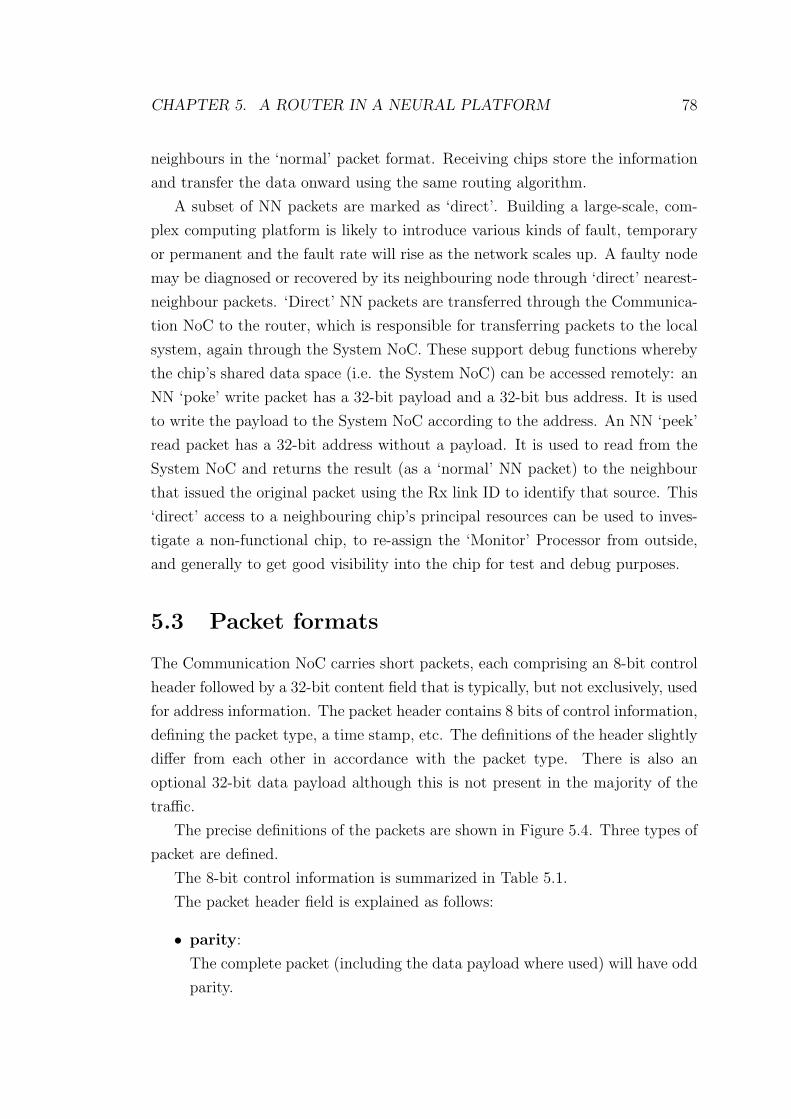
CHAPTER 5. A ROUTER IN A NEURAL PLATFORM 78
neighbours in the ‘normal’ packet format. Receiving chips store the information
and transfer the data onward using the same routing algorithm.
A subset of NN packets are marked as ‘direct’. Building a large-scale, com-
plex computing platform is likely to introduce various kinds of fault, temporary
or permanent and the fault rate will rise as the network scales up. A faulty node
may be diagnosed or recovered by its neighbouring node through ‘direct’ nearest-
neighbour packets. ‘Direct’ NN packets are transferred through the Communica-
tion NoC to the router, which is responsible for transferring packets to the local
system, again through the System NoC. These support debug functions whereby
the chip’s shared data space (i.e. the System NoC) can be accessed remotely: an
NN ‘poke’ write packet has a 32-bit payload and a 32-bit bus address. It is used
to write the payload to the System NoC according to the address. An NN ‘peek’
read packet has a 32-bit address without a payload. It is used to read from the
System NoC and returns the result (as a ‘normal’ NN packet) to the neighbour
that issued the original packet using the Rx link ID to identify that source. This
‘direct’ access to a neighbouring chip’s principal resources can be used to inves-
tigate a non-functional chip, to re-assign the ‘Monitor’ Processor from outside,
and generally to get good visibility into the chip for test and debug purposes.
5.3 Packet formats
The Communication NoC carries short packets, each comprising an 8-bit control
header followed by a 32-bit content field that is typically, but not exclusively, used
for address information. The packet header contains 8 bits of control information,
defining the packet type, a time stamp, etc. The definitions of the header slightly
differ from each other in accordance with the packet type. There is also an
optional 32-bit data payload although this is not present in the majority of the
traffic.
The precise definitions of the packets are shown in Figure 5.4. Three types of
packet are defined.
The 8-bit control information is summarized in Table 5.1.
The packet header field is explained as follows:
• parity:
The complete packet (including the data payload where used) will have odd
parity.

CHAPTER 5. A ROUTER IN A NEURAL PLATFORM 79
NormalRouteType = 10
/DirectParityData
Header Data payloadAddress / Operation
Type = 01 ParityDataTimestampcodeSequence
Header Source ID Destination ID Data payload
Type = 00 routingEmergency
ParityDataTimestamp
Header Routing key (Data payload)
Type = 11
(Reserved packet type)
Nearest−neighbour Packet
Point−to−point Packet
Multicast Packet
Figure 5.4: Packet formats
• data:
Indicates whether the packet has a 32-bit data payload (data = 1) or not
(data = 0).
• time stamp:
The system has a global time phase that cycles through 00 → 01 → 11 →10→ 00. Global synchronisation must be accurate to within less than one
time phase (the duration of which is programmable and may be dynamically
variable). A packet is launched with a time stamp equal to the current time

CHAPTER 5. A ROUTER IN A NEURAL PLATFORM 80
Field Name bits Function
parity 0 parity of complete packet (including payload whenused)
data 1 data payload (1) or no data payload (0)time stamp 3:2 phase marker indicating time packet was launchedseq code 5:4 P2P packet only: start, middle odd/even, end of
payloademergency routing 5:4 MC packet only: used to control routing around a
failed linkroute 4:2 NN packet only: information for the routerT: nn packet type 5 NN packet only: packet type - normal (0) or
direct (1)packet type 7:6 00 for MC packet; 01 for P2P; 10 for NN
Table 5.1: Packet header summary
phase; and if a router finds a packet that is two time phases old (current
time phase XOR packet time phase = 11) it will drop it to the local Monitor
Processor. The time stamp is inserted by the local router.
• seq code:
P2P packets use these bits to indicate the sequence of data payloads:
11 → start packet: the first packet in a sequence (of >1 packets).
10 → middle even: the second, fourth, sixth, ... packet in a sequence.
01 → middle odd: the third, fifth, seventh, ... packet in a sequence.
00 → end: the last (or only) packet in a sequence.
• emergency routing:
MC packets use these bits to control emergency routing around a failed or
congested link:
00 → normal MC packet;
01 → the packet has been redirected by the previous router through an
emergency route along with a normal copy of the packet. The receiving
router should treat this as a combined normal plus emergency packet.
10 → the packet has been redirected by the previous router through an
emergency route which would not be used for a normal packet.
11 → this emergency packet is reverting to its normal route.
CHAPTER 5. A ROUTER IN A NEURAL PLATFORM 81
• route:
These bits enable an NN packet to be directed to a particular neighbour (0
- 5), to all neighbours (6), or to the local Monitor Processor (7).
• T (NN packet type):
This bit specifies whether an NN packet is ‘normal’, so that it is delivered
to the Monitor Processor on the neighbouring chip(s), or ‘direct’, so that
the Monitor Processor performs a read or write access to the neighbouring
chip’s System NoC resource.
• packet type:
These bits indicate whether the packet is a multicast (00), point-to-point
(01) or nearest-neighbour (10) packet.
5.4 Adaptive routing
Biological neural networks exhibit considerable fault-tolerance and are able to
maintain their functionality even in the presence of small lesions. This ‘fault-
tolerant’ characteristic is exploitable in large-scale neural network simulations to
overcome hardware failure, especially in a real-time application. This is necessary
to minimize the probability that transient congestion will cause delays sufficient to
perturb the real-time assumptions. The approach adopted is to buffer the packet
by making use of the empty pipeline stages of the router. Another measure is
adaptive routing which handles the situation of buffer overflow.
To achieve adaptive routing, the network must have enough redundancy to
maintain its real-time performance when part of the network is congested because
of a transient or a permanent failure. The SpiNNaker system has a 2-dimensional
toroidal triangular mesh topology which can offer some redundancy by automat-
ically redirecting a blocked packet through adjacent links (emergency route) to
its destination. This redirecting mechanism is called ‘adaptive routing’ and is
provided by an adaptive routing controller at the output routing stage. When
congestion occurs, the controller counts the number of clock cycles that the packet
has been blocked. When the number of cycles reaches a threshold, the controller
will then attempt to direct the packet to its emergency route.
CHAPTER 5. A ROUTER IN A NEURAL PLATFORM 82
The algorithm of adaptive routing, described in pseudo-code, is given in ap-
pendix A.
An example of adaptive routing is shown in Figure 5.5, where a packet is issued
at node ‘O’, destined for the target node ‘T’ along the dotted arrow line. If the
link between node ‘I’ and node ‘D’ marked ‘a’ is congested or broken, the adaptive
routing controller at node ‘I’ will sense back pressure from link ‘a’ and redirect
the blocked packet via links ‘b’ and ‘c’ as the emergency route. The packet is
tagged in its header [5:4] (emergency route) so that node ‘E’, and subsequently
node ‘D’ are able to get it on track again despite not containing appropriate
routing tables. If the emergency route also fails, the packet will be dropped and
handled by the local system. If the packets to node ‘D’ are constantly dropped,
the system will treat this node as an permanent failed one and will re-program
the routing tables in the neighbouring nodes to avoid this node.
O
D
D TI
b c
a
E
Figure 5.5: An example of adaptive routing
5.5 Router configurations
As SpiNNaker is designed for experimental purposes, it is important that the
system can adapt to different neural simulations with low overheads for differ-
ent tasks. In these tasks, neural simulations vary in terms of network scale,
computation algorithm, interconnect topology, etc. Therefore, scalability, pro-
grammability and flexibility are the desired features for the neural simulation
platform.
CHAPTER 5. A ROUTER IN A NEURAL PLATFORM 83
As a large, parallel computation platform with thousands of elements, SpiN-
Naker needs an efficient housekeeping mechanism for programming, administra-
tion, test and verification. This mechanism is distributed to each node, under
the control of the local Monitor Processors. The router is the central unit to
realise data distribution. This section discusses the router’s communication algo-
rithm that supports the housekeeping features of the large-scale neural platform.
The architecture to conduct the communication is built upon the Communica-
tion NoC, which provides router-to-router interconnects, and the System NoC,
which provides router-to-system interconnects. The router, therefore, bridges the
communication between the two networks.
For configuration purposes, the Host system sends programming data to the
local Monitor Processor at each node. The programming data can be configura-
tion information to a router or to other peripherals on the System NoC. Most of
the system configuration, such as neuron interconnects, rely on the programming
of the router. Here the router is a slave of the System NoC, through which the
local Monitor Processor configures its routing tables and control registers.
Neuron placement and routing is done by the Host system. This information
is distributed, as appropriate, to each chip’s Monitor Processor using nearest-
neighbour hops carrying data payloads.
For administrative purposes, the operating system needs to monitor the router
status to perform configuration operations and detect errors. The information can
be in the form of a dumped packet, an interrupt, or traffic statistic. This requires
the router to be readable by the local Monitor Processor through the System
NoC.
5.5.1 Routing table configuration
The router’s routing tables and registers are configurable and readable via the
System NoC. The contents of the routing tables and their addresses are defined
in Table 5.2.
The MC key table and the MC mask table are stored in the CAM. As shown in
Figure 5.6, an MC packet’s key is masked with all entries in the CAM. If a match
is found, the corresponding RAM entry is read indicating routing destination(s).
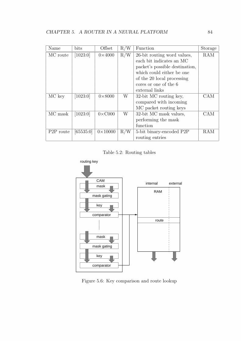
CHAPTER 5. A ROUTER IN A NEURAL PLATFORM 84
Name bits Offset R/W Function Storage
MC route [1023:0] 0×4000 R/W 26-bit routing word values, RAMeach bit indicates an MCpacket’s possible destination,which could either be oneof the 20 local processingcores or one of the 6external links
MC key [1023:0] 0×8000 W 32-bit MC routing key, CAMcompared with incomingMC packet routing keys
MC mask [1023:0] 0×C000 W 32-bit MC mask values, CAMperforming the maskfunction
P2P route [65535:0] 0×10000 R/W 5-bit binary-encoded P2P RAMrouting entries
Table 5.2: Routing tables
key
mask
mask gating
comparator
CAM
key
mask
mask gating
comparator
route
RAM
internal external
routing key
Figure 5.6: Key comparison and route lookup

CHAPTER 5. A ROUTER IN A NEURAL PLATFORM 85
5.5.2 Register configuration
The router has a set of configuration registers, some are used to store setup
information for the router. This information defines the router’s properties, such
as the maximum waiting time for adaptive routing or the current time phase of
the network. Other registers are used to store the router’s status information,
such as a blocked routing port number. By reading this information the Monitor
Processor can observe the status of the network and identify errors. The registers’
detailed definitions are found in appendix B.
5.5.3 Programmable diagnostic counters
For monitoring purposes, the router also has eight programmable diagnostic coun-
ters to count packets passing through it. They count a certain type of packet
according to pre-loaded configurations so that the system can monitor the statis-
tical population of packets. A diagnostic counter may (optionally) generate an
interrupt on each count. There are three types of registers in the counters.
Counter enable/reset filter
Each of these counters can be used to count selected types of packets under
the control of the corresponding counter enable/reset filter (Figure 5.7). This
filter provides a single control point for the 8 diagnostic counters, enabling them
to count events over a precisely controlled time period.
29 28 27 26 25 24 23 22 21 20 19 16 15 14 13 12 11 10 9 8 7 6 5 4 3 2 1 018 1731 30
reset[7:0] enable[7:0]
Figure 5.7: Counter filter register
The functions of bits in the filter are described in Table 5.3.
Name bits R/W Function
enable[7:0] 7:0 R/W enable diagnostic counter 7..0reset[7:0] 23:16 W write a 1 to reset diagnostic counter 7..0
Table 5.3: Diagnostic counter enable/reset
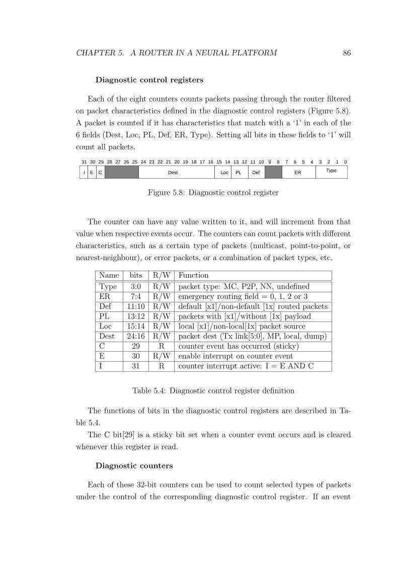
CHAPTER 5. A ROUTER IN A NEURAL PLATFORM 86
Diagnostic control registers
Each of the eight counters counts packets passing through the router filtered
on packet characteristics defined in the diagnostic control registers (Figure 5.8).
A packet is counted if it has characteristics that match with a ‘1’ in each of the
6 fields (Dest, Loc, PL, Def, ER, Type). Setting all bits in these fields to ‘1’ will
count all packets.
29 28 27 26 25 24 23 22 21 20 19 16 15 14 13 12 11 10 9 8 7 6 5 4 3 2 1 018 1731 30
CI E Dest Loc PL Def ER Type
Figure 5.8: Diagnostic control register
The counter can have any value written to it, and will increment from that
value when respective events occur. The counters can count packets with different
characteristics, such as a certain type of packets (multicast, point-to-point, or
nearest-neighbour), or error packets, or a combination of packet types, etc.
Name bits R/W Function
Type 3:0 R/W packet type: MC, P2P, NN, undefinedER 7:4 R/W emergency routing field = 0, 1, 2 or 3Def 11:10 R/W default [x1]/non-default [1x] routed packetsPL 13:12 R/W packets with [x1]/without [1x] payloadLoc 15:14 R/W local [x1]/non-local[1x] packet sourceDest 24:16 R/W packet dest (Tx link[5:0], MP, local, dump)C 29 R counter event has occurred (sticky)E 30 R/W enable interrupt on counter eventI 31 R counter interrupt active: I = E AND C
Table 5.4: Diagnostic control register definition
The functions of bits in the diagnostic control registers are described in Ta-
ble 5.4.
The C bit[29] is a sticky bit set when a counter event occurs and is cleared
whenever this register is read.
Diagnostic counters
Each of these 32-bit counters can be used to count selected types of packets
under the control of the corresponding diagnostic control register. If an event
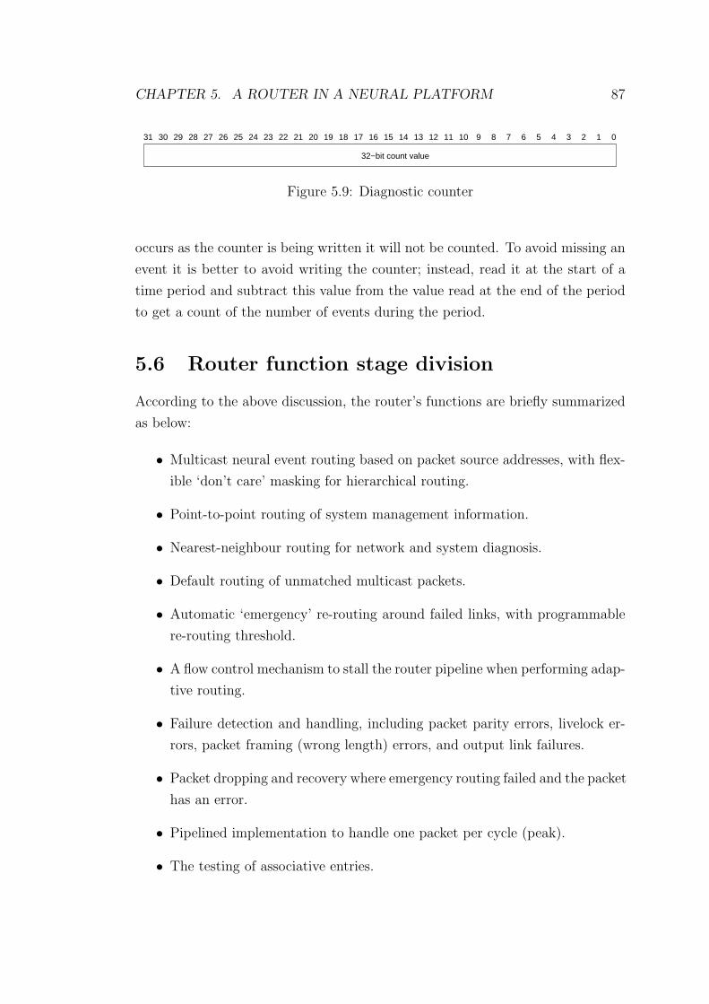
CHAPTER 5. A ROUTER IN A NEURAL PLATFORM 87
29 28 27 26 25 24 23 22 21 20 19 16 15 14 13 12 11 10 9 8 7 6 5 4 3 2 1 018 1731 30
32−bit count value
Figure 5.9: Diagnostic counter
occurs as the counter is being written it will not be counted. To avoid missing an
event it is better to avoid writing the counter; instead, read it at the start of a
time period and subtract this value from the value read at the end of the period
to get a count of the number of events during the period.
5.6 Router function stage division
According to the above discussion, the router’s functions are briefly summarized
as below:
• Multicast neural event routing based on packet source addresses, with flex-
ible ‘don’t care’ masking for hierarchical routing.
• Point-to-point routing of system management information.
• Nearest-neighbour routing for network and system diagnosis.
• Default routing of unmatched multicast packets.
• Automatic ‘emergency’ re-routing around failed links, with programmable
re-routing threshold.
• A flow control mechanism to stall the router pipeline when performing adap-
tive routing.
• Failure detection and handling, including packet parity errors, livelock er-
rors, packet framing (wrong length) errors, and output link failures.
• Packet dropping and recovery where emergency routing failed and the packet
has an error.
• Pipelined implementation to handle one packet per cycle (peak).
• The testing of associative entries.
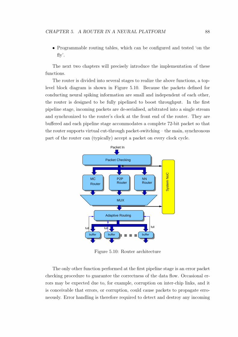
CHAPTER 5. A ROUTER IN A NEURAL PLATFORM 88
• Programmable routing tables, which can be configured and tested ‘on the
fly’.
The next two chapters will precisely introduce the implementation of these
functions.
The router is divided into several stages to realize the above functions, a top-
level block diagram is shown in Figure 5.10. Because the packets defined for
conducting neural spiking information are small and independent of each other,
the router is designed to be fully pipelined to boost throughput. In the first
pipeline stage, incoming packets are de-serialised, arbitrated into a single stream
and synchronized to the router’s clock at the front end of the router. They are
buffered and each pipeline stage accommodates a complete 72-bit packet so that
the router supports virtual cut-through packet-switching – the main, synchronous
part of the router can (typically) accept a packet on every clock cycle.
full full full
bufferbufferbuffer
MUX
Adaptive Routing
Packet Checking
Packet In
MC
Router
P2PRouter
NNRouter
Sys
tem
NoC
Figure 5.10: Router architecture
The only other function performed at the first pipeline stage is an error packet
checking procedure to guarantee the correctness of the data flow. Occasional er-
rors may be expected due to, for example, corruption on inter-chip links, and it
is conceivable that errors, or corruption, could cause packets to propagate erro-
neously. Error handling is therefore required to detect and destroy any incoming
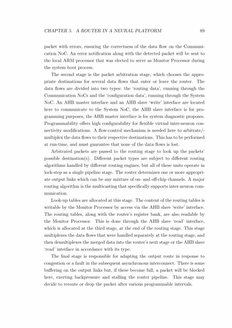
CHAPTER 5. A ROUTER IN A NEURAL PLATFORM 89
packet with errors, ensuring the correctness of the data flow on the Communi-
cation NoC. An error notification along with the detected packet will be sent to
the local ARM processor that was elected to serve as Monitor Processor during
the system boot process.
The second stage is the packet arbitration stage, which chooses the appro-
priate destinations for several data flows that enter or leave the router. The
data flows are divided into two types: the ‘routing data’, running through the
Communication NoCs and the ‘configuration data’, running through the System
NoC. An AHB master interface and an AHB slave ‘write’ interface are located
here to communicate to the System NoC, the AHB slave interface is for pro-
gramming purposes, the AHB master interface is for system diagnostic proposes.
Programmability offers high configurability for flexible virtual inter-neuron con-
nectivity modifications. A flow-control mechanism is needed here to arbitrate/-
multiplex the data flows to their respective destinations. This has to be performed
at run-time, and must guarantee that none of the data flows is lost.
Arbitrated packets are passed to the routing stage to look up the packets’
possible destination(s). Different packet types are subject to different routing
algorithms handled by different routing engines, but all of these units operate in
lock-step as a single pipeline stage. The router determines one or more appropri-
ate output links which can be any mixture of on- and off-chip channels. A major
routing algorithm is the multicasting that specifically supports inter-neuron com-
munication.
Look-up tables are allocated at this stage. The content of the routing tables is
writable by the Monitor Processor by access via the AHB slave ‘write’ interface.
The routing tables, along with the router’s register bank, are also readable by
the Monitor Processor. This is done through the AHB slave ‘read’ interface,
which is allocated at the third stage, at the end of the routing stage. This stage
multiplexes the data flows that were handled separately at the routing stage, and
then demultiplexes the merged data into the router’s next stage or the AHB slave
‘read’ interface in accordance with its type.
The final stage is responsible for adapting the output route in response to
congestion or a fault in the subsequent asynchronous interconnect. There is some
buffering on the output links but, if these become full, a packet will be blocked
here, exerting backpressure and stalling the router pipeline. This stage may
decide to reroute or drop the packet after various programmable intervals.
CHAPTER 5. A ROUTER IN A NEURAL PLATFORM 90
In addition to the function stages, the router has two sets of adapters to the
asynchronous interconnect. One set includes the input and output adapters to
the Communication NoC. There is one input adapter for receiving packets from
the arbiter and 26 or so output adapters to the outgoing links. The second set
includes the transmitting and receiving adapters for the AHB interfaces.
5.7 Summary
This chapter gave an overview of the function and performance requirements
of a pipelined router which is designed specifically for neural simulations on a
multi-chip MPSoC system – SpiNNaker. It has a principal target of support-
ing real-time multicast neural event routing. It also supports point-to-point and
nearest-neighbour routing which are used for different purpose, such as debugging
and programming, but use the same network. An adaptive routing mechanism,
specially for multicasting, was introduced. As an experimental platform, SpiN-
Naker can also be run-time programmed, configured and monitored. The router is
designed to support these functions. It is divided into several blocks by functions.
The next chapter focuses on the implementation of these blocks.
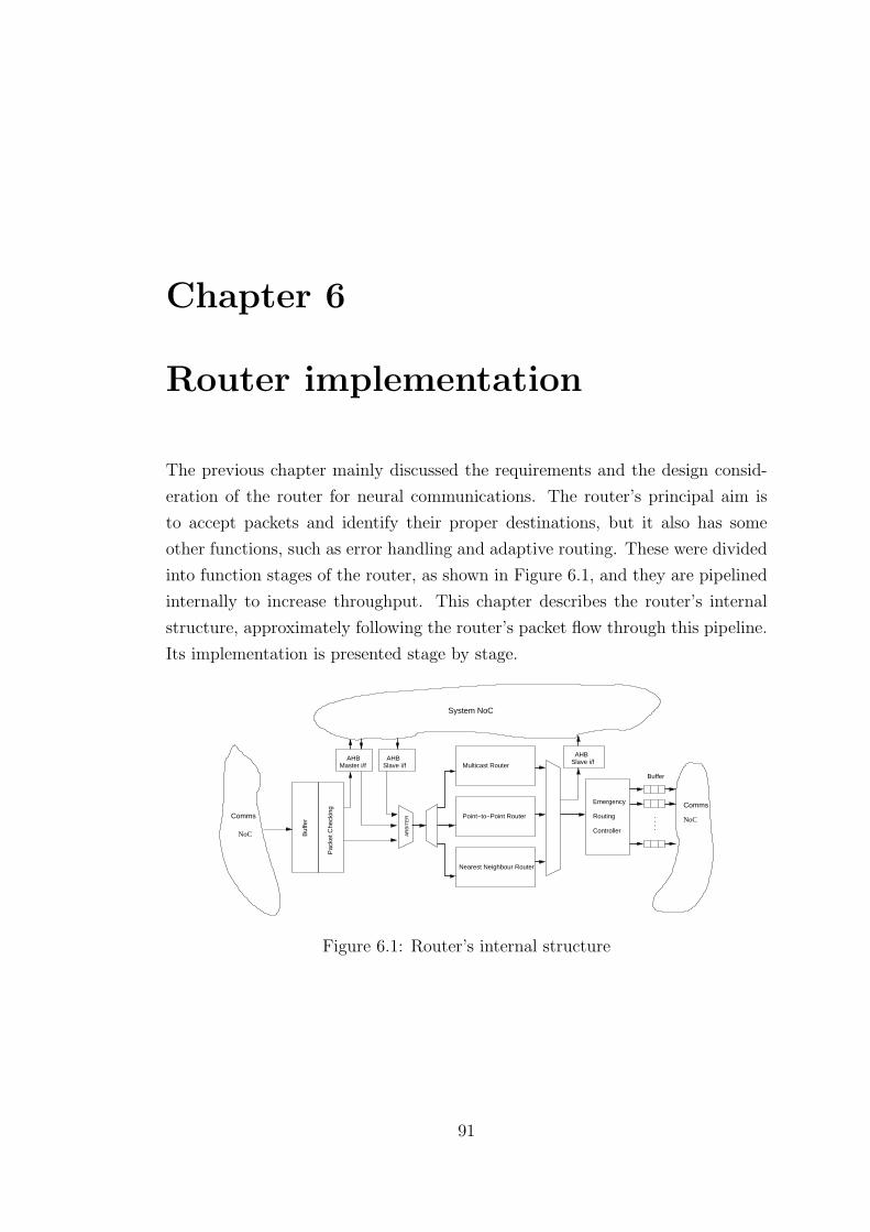
Chapter 6
Router implementation
The previous chapter mainly discussed the requirements and the design consid-
eration of the router for neural communications. The router’s principal aim is
to accept packets and identify their proper destinations, but it also has some
other functions, such as error handling and adaptive routing. These were divided
into function stages of the router, as shown in Figure 6.1, and they are pipelined
internally to increase throughput. This chapter describes the router’s internal
structure, approximately following the router’s packet flow through this pipeline.
Its implementation is presented stage by stage.
Nearest Neighbour Router
Point−to−Point Router
Multicast Router
System NoC
Buffer
Master i/f Slave i/f Slave i/f
Comms
NoC
Buf
fer
Pac
ket C
heck
ing
AR
BIT
ER
Emergency
Routing
Controller
AHB AHBAHB
NoC
Comms
Figure 6.1: Router’s internal structure
91

CHAPTER 6. ROUTER IMPLEMENTATION 92
6.1 Error handling
One prerequisite of routing is to maintain the correctness of data transporta-
tion over the interconnection network. The first functional stage of the router,
therefore, handles errors in the incoming packets. Three common errors can be
handled:
• A transient bit error may happen on interconnection networks, resulting in
one, or more, error bits in a certain packet. Although the failure rate on
individual components is normally low, the overall number of error packets
in a large-scale network with thousands of components can be unacceptable.
A certain level of transient bit error can easily be detected by parity check-
ing. A parity error can happen in either the asynchronous or synchronous
parts of the system, and it will be checked inside the router.
• Because the data on the asynchronous link channels is serialized into 4-bit
flits, any loss of a flit on those channels will cause an incomplete packet to
be received. This situation is identified as a framing error which is detected
when the flits are being assembled into a packet.
• It is undesirable to allow a livelocked packet to remain in the network
forever. To avoid this, a simple mechanism is employed where each packet
includes a time phase field. A rough elapsed time system therefore detects
and destroys any incoming packet which is too old to be useful any longer.
The time stamp comprises 2 bits, cycling 00 → 01 → 11 → 10. When the
packet is two time phases old it is dropped to the local Monitor Processor.
The length of a time phase can be adapted dynamically to the state of the
system; normally, timed-out packets should be very rare so the time phase
can be conservatively long to minimize the risk of packets being dropped
due to congestion. The time-phase information is maintained across the
system by software running on the Monitor Processors.
Any input error causes the packet to be taken out of circulation. The packet
contents, as recovered, are dropped to a diagnostic register (Figure 6.2) which can
assert an interrupt. Error recovery is a software task for the Monitor Processor.
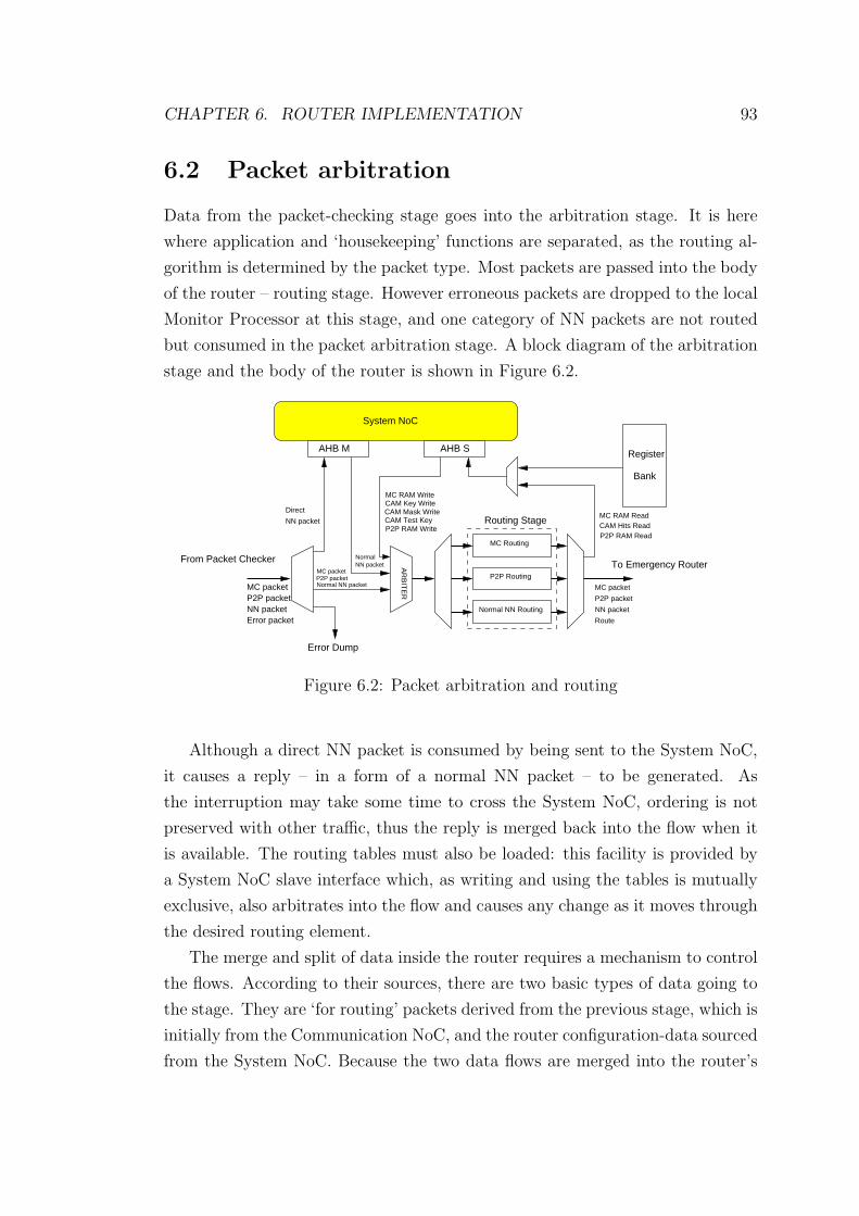
CHAPTER 6. ROUTER IMPLEMENTATION 93
6.2 Packet arbitration
Data from the packet-checking stage goes into the arbitration stage. It is here
where application and ‘housekeeping’ functions are separated, as the routing al-
gorithm is determined by the packet type. Most packets are passed into the body
of the router – routing stage. However erroneous packets are dropped to the local
Monitor Processor at this stage, and one category of NN packets are not routed
but consumed in the packet arbitration stage. A block diagram of the arbitration
stage and the body of the router is shown in Figure 6.2.
AR
BIT
ER
From Packet Checker
CAM Test KeyCAM Mask WriteCAM Key WriteMC RAM Write
P2P RAM ReadCAM Hits ReadMC RAM Read
NN packet
Direct
Error Dump
AHB M AHB S
System NoC
Bank
Register
NN packetNormal
P2P packetMC packet
Normal NN packet
Normal NN Routing
MC Routing
P2P Routing
To Emergency Router
MC packet
P2P packet
NN packet
Route
Routing Stage
P2P packetMC packet
NN packetError packet
P2P RAM Write
Figure 6.2: Packet arbitration and routing
Although a direct NN packet is consumed by being sent to the System NoC,
it causes a reply – in a form of a normal NN packet – to be generated. As
the interruption may take some time to cross the System NoC, ordering is not
preserved with other traffic, thus the reply is merged back into the flow when it
is available. The routing tables must also be loaded: this facility is provided by
a System NoC slave interface which, as writing and using the tables is mutually
exclusive, also arbitrates into the flow and causes any change as it moves through
the desired routing element.
The merge and split of data inside the router requires a mechanism to control
the flows. According to their sources, there are two basic types of data going to
the stage. They are ‘for routing’ packets derived from the previous stage, which is
initially from the Communication NoC, and the router configuration-data sourced
from the System NoC. Because the two data flows are merged into the router’s

CHAPTER 6. ROUTER IMPLEMENTATION 94
datapath at this stage, there can be more than one request issued by different
interfaces in the same clock cycle. When this happens, arbitration is needed,
letting the interface with the highest priority enter the datapath while any others
stall. An arbiter is located after packet multiplexing to decide the sequence of
the flows. The priorities for its decision are (from the highest to the lowest):
• AHB master requests (from ‘direct’ nearest-neighbour ‘peek’ and ‘poke’
packets)
• AHB slave requests (from write requests to the multicast key table, multi-
cast mask table, multicast routing table, point-to-point routing table, and
router register bank)
• Routing requests (from multicast routing, point-to-point routing, and ‘nor-
mal’ nearest-neighbour routing)
The arbitrated data is then sent to the appropriate routing engine of the
routing stage. The data can be either routing information that derives routing
destination(s) from a routing engine or a ‘write’ or ‘read’ request to a routing
table or register. In practice, traffic is expected to be sparse, so any stalls should
be short.
6.3 Routing stage
Arbitrated packets are passed through the routing stage, which incorporates the
routing engines, to identify the packet’s possible destination(s). The routing of
each type of packet is very different. Therefore, a packet is sent to an appropriate
router with control information, in parallel, ensuring that it is collected at the
appropriate time.
6.3.1 Multicast routing
An efficient multicast routing mechanism is implemented to emulate the one-to-
many communication in neural networks. Multicasting scenarios are well devel-
oped for macro-networks [RC96][THH01][SZX07], however it is not possible to
transfer these scenarios into micro-networks. Due to its limited power and area
budget, on-chip multicast router design requires new architectural considerations
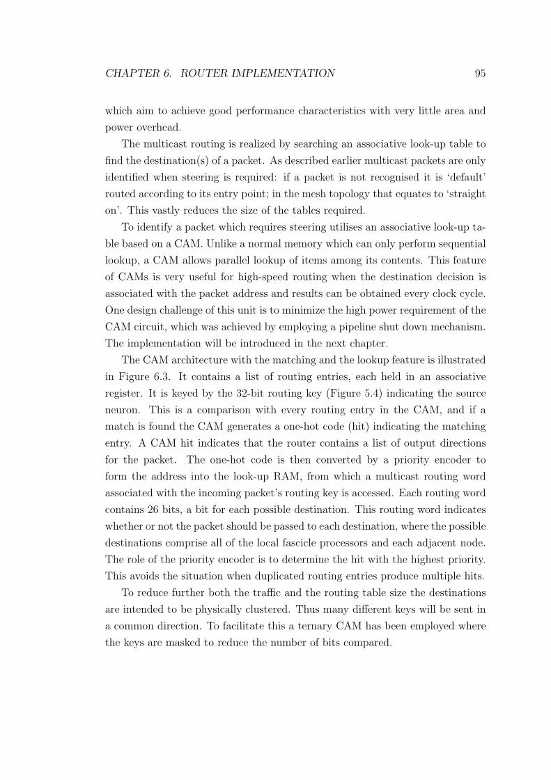
CHAPTER 6. ROUTER IMPLEMENTATION 95
which aim to achieve good performance characteristics with very little area and
power overhead.
The multicast routing is realized by searching an associative look-up table to
find the destination(s) of a packet. As described earlier multicast packets are only
identified when steering is required: if a packet is not recognised it is ‘default’
routed according to its entry point; in the mesh topology that equates to ‘straight
on’. This vastly reduces the size of the tables required.
To identify a packet which requires steering utilises an associative look-up ta-
ble based on a CAM. Unlike a normal memory which can only perform sequential
lookup, a CAM allows parallel lookup of items among its contents. This feature
of CAMs is very useful for high-speed routing when the destination decision is
associated with the packet address and results can be obtained every clock cycle.
One design challenge of this unit is to minimize the high power requirement of the
CAM circuit, which was achieved by employing a pipeline shut down mechanism.
The implementation will be introduced in the next chapter.
The CAM architecture with the matching and the lookup feature is illustrated
in Figure 6.3. It contains a list of routing entries, each held in an associative
register. It is keyed by the 32-bit routing key (Figure 5.4) indicating the source
neuron. This is a comparison with every routing entry in the CAM, and if a
match is found the CAM generates a one-hot code (hit) indicating the matching
entry. A CAM hit indicates that the router contains a list of output directions
for the packet. The one-hot code is then converted by a priority encoder to
form the address into the look-up RAM, from which a multicast routing word
associated with the incoming packet’s routing key is accessed. Each routing word
contains 26 bits, a bit for each possible destination. This routing word indicates
whether or not the packet should be passed to each destination, where the possible
destinations comprise all of the local fascicle processors and each adjacent node.
The role of the priority encoder is to determine the hit with the highest priority.
This avoids the situation when duplicated routing entries produce multiple hits.
To reduce further both the traffic and the routing table size the destinations
are intended to be physically clustered. Thus many different keys will be sent in
a common direction. To facilitate this a ternary CAM has been employed where
the keys are masked to reduce the number of bits compared.
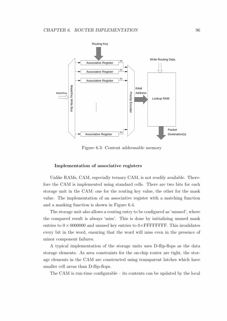
CHAPTER 6. ROUTER IMPLEMENTATION 96
Associative Register
Associative Register
Associative Register
Routing Key
hit
hit
hit
hit
Associative Register
Address
RAM
Write Routing Data
Lookup RAMP
riority Encoder
Mask/K
ey Write B
us
Mask/Key
Packet
Destination(s)
Figure 6.3: Content addressable memory
Implementation of associative registers
Unlike RAMs, CAM, especially ternary CAM, is not readily available. There-
fore the CAM is implemented using standard cells. There are two bits for each
storage unit in the CAM: one for the routing key value, the other for the mask
value. The implementation of an associative register with a matching function
and a masking function is shown in Figure 6.4.
The storage unit also allows a routing entry to be configured as ‘unused’, where
the compared result is always ‘miss’. This is done by initializing unused mask
entries to 0× 0000000 and unused key entries to 0×FFFFFFFF. This invalidates
every bit in the word, ensuring that the word will miss even in the presence of
minor component failures.
A typical implementation of the storage units uses D-flip-flops as the data
storage elements. As area constraints for the on-chip router are tight, the stor-
age elements in the CAM are constructed using transparent latches which have
smaller cell areas than D-flip-flops.
The CAM is run-time configurable – its contents can be updated by the local
CHAPTER 6. ROUTER IMPLEMENTATION 97
32
E
DD
E
Routing Keyhit
key in
mask WrEn key WrEn
mask
1100
key
0101
result
match 0match 1hitmiss
− masking the key − disabling the key
mask in
Figure 6.4: Associative register
Monitor Processor. This requires keeping the current state stable while config-
uring the device. Because latches are designed to be transparent, they change
their output signals immediately after the inputs change when enabled. This is
likely to cause timing violations when using a latch in a sequential machine if
the data signal (‘D’) changes between the setup and hold times. To avoid this
potential problem, the presentation of the data on the AHB slave interface has
to be held for two clock cycles in each ‘write’ operation. The previous pipeline
needs to be stalled to prevent absorbing any new packet until the write operation
has completed. The timing diagram is shown in Figure 6.5. Timing is controlled
by a state machine which holds the data signal for two clock cycles and holds the
enable signal (‘G’) for only one clock cycle; the rising and the falling of the enable
signal are triggered by the negative edges to guarantee that the data signal does
not violate the setup and hold times.
The layout area of the 1024-entry CAM using transparent latches can be
compared with that using D-flip-flops on a UMC 130-nm CMOS technology,
where the area of the 1×-drive strength latch is 15.68 µm2, and that of the 1×-
drive strength D-flip-flop is 29.12 µm2. The total area saved is thus approximately
46% (0.9 mm2). Because the CAM occupies about 60% of the router’s total area,
this is a significant reduction of the area.
A custom-built VLSI CAM would reduce this further. A custom-built CAM
typically replaces the latches by SRAM cells for bit storage and uses equivalent
logic for bit comparison and masking, which is the same as that in the CAM in the

CHAPTER 6. ROUTER IMPLEMENTATION 98
Data 1 Data 2Q
D
G
Q
CLOCK
Data 1 Data 2D
G
rs = Required setup time
rh = Required hold time
rs rh
th = Actual etup time
ts
ts = Actual Setup time
th
Figure 6.5: Timing diagram of the CAM
SpiNNaker router. The SRAM storage and access transistors, which are used to
read and write the SRAM storage, account for 6 transistors [PS06], while the latch
cell on the UMC 130-nm CMOS process uses 18 transistors. As a result, 768K
(32×2×(18-6)×1024) transistors are saved in a 1024×32-bit custom-built ternary
CAM. Because the total transistor count of the standard cell CAM reported by
Cadence Layout Editor is about 1,500 K, the custom-built CAM reduces the
transistor number by half.
In order to compare the area of the custom-built CAM to that of the standard
cell design, the difference in layout density should also be considered. A custom-
built circuit can employ minimum-sized transistors and a compact layout because
wire loads and lengths are optimum. Dally describes an example where a custom-
built circuit has an area of about 1/8 that of the standard cell design with the
same structure [DC00]. Since the custom-built CAM has halved the number
of transistor, its area can be estimated to be 16 times smaller than that of the
standard cell design. However, a custom-built CAM would be expensive to design
and reduce process portability. The fully-portable standard cell CAM yields a size
approximately equal to that of the ARM968 processor node used on SpiNNaker,
which is considered acceptable.
CAM test scenario
The degree of hard defects for process technologies is still high: it is estimated

CHAPTER 6. ROUTER IMPLEMENTATION 99
that the defect density of VLSI over the next five years will be constant at 1.4K
defects/m2 chip area but the number of transistors per unit doubles every 2∼3
years [Pat07]. As the CAM occupies the main part of the router, the majority of
the router’s die area will be taken by the CAM. A small version of a SpiNNaker
system, such as a 4 × 4 network, has a large number (16K × 32-bit) of CAM
entries to be manufactured and tested. As the CAM compares a key to all its
entries in parallel, a dead gate in a single entry can lead to wrong results for
many or all comparisons. A defect has to be testable and preferably quarantined
so that the router can function with a certain level of failure.
For the sake of area efficiency, the CAM is not designed to be directly readable
by the Monitor Processor, so the system has to adopt a test scenario where the
Monitor Processor inserts a test key to the CAM and checks if the correspond-
ing ‘match’ or ‘miss’ result is as expected. More precisely, the defect detection
compromises the steps of:
• A ‘match’ test first sets a value to the entry under test, and then presents a
test routing key with the same value to check if it scores a hit at this entry
as it should do.
• A ‘miss’ test checks if a key misses at a 32-bit entry whenever 1 bit is
different. This is the expensive part of the CAM test, which can be done
on all entries in parallel.
To explain the scenario, a small-scale of example with a 4-entry 4-bit CAM is
presented below:
For testing the CAM for ‘matches’, the CAM keys are first set to:
0001001001001000
Then the Monitor Processor presents the test routing keys ‘0001, 0010, 0100,
1000’ to a test register, which is used to perform a key comparison to the CAM.
A comparison is triggered by an AHB read request to another test register, which
stores the corresponding ‘hits’. The hit bits are encoded as binary codes, which
are read from Register T1 to check if they hits at the expected places.

CHAPTER 6. ROUTER IMPLEMENTATION 100
The efficient way to test the CAM for ‘misses’ is to set all entries to the
same value, then to present a test routing key that differs in one bit only. The
procedure is first to set the CAM to:
0101010101010101
Then apply input keys ‘0100, 0111, 0001, 1101’.
Then the CAM is set to the corresponding value:
1010101010101010
Then apply input keys ‘1011, 1000, 1110, 0010’.
For all of these keys all entries should miss. If the CAM scores any hit, this
is an error. If any defect is detected in a entry, the entry should be quarantined.
The quarantine function is realized by setting the key value of that entry to
0×FFFFFFFF, and the mask value to 0× 0000000.
In summary, to perform the test and the quarantine scenario, it is necessary
to ensure that the Monitor processor can:
• Write every entry and mask bit.
• Present any routing key.
• Read the hit (and encoded output bits) that the routing key generates.
6.3.2 Point-to-point routing
P2P routing is for communication between chips, not neurons or even processors.
Only the Monitor Processor on each chip uses these packets which means that
the addressing problem is reduced. A 16-bit destination field means that a 64K
chip system can be built and a lookup of this size is feasible in RAM, especially
as only 3 bits/entry are required (Table 6.1).
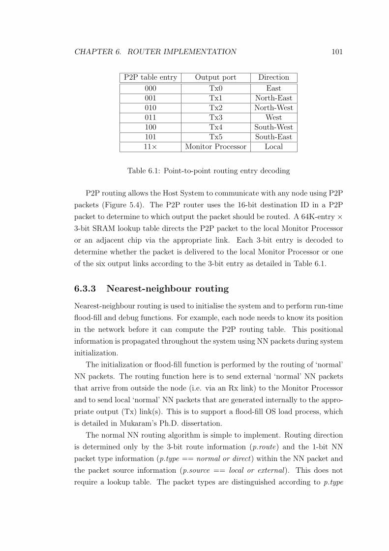
CHAPTER 6. ROUTER IMPLEMENTATION 101
P2P table entry Output port Direction
000 Tx0 East001 Tx1 North-East010 Tx2 North-West011 Tx3 West100 Tx4 South-West101 Tx5 South-East11× Monitor Processor Local
Table 6.1: Point-to-point routing entry decoding
P2P routing allows the Host System to communicate with any node using P2P
packets (Figure 5.4). The P2P router uses the 16-bit destination ID in a P2P
packet to determine to which output the packet should be routed. A 64K-entry ×3-bit SRAM lookup table directs the P2P packet to the local Monitor Processor
or an adjacent chip via the appropriate link. Each 3-bit entry is decoded to
determine whether the packet is delivered to the local Monitor Processor or one
of the six output links according to the 3-bit entry as detailed in Table 6.1.
6.3.3 Nearest-neighbour routing
Nearest-neighbour routing is used to initialise the system and to perform run-time
flood-fill and debug functions. For example, each node needs to know its position
in the network before it can compute the P2P routing table. This positional
information is propagated throughout the system using NN packets during system
initialization.
The initialization or flood-fill function is performed by the routing of ‘normal’
NN packets. The routing function here is to send external ‘normal’ NN packets
that arrive from outside the node (i.e. via an Rx link) to the Monitor Processor
and to send local ‘normal’ NN packets that are generated internally to the appro-
priate output (Tx) link(s). This is to support a flood-fill OS load process, which
is detailed in Mukaram’s Ph.D. dissertation.
The normal NN routing algorithm is simple to implement. Routing direction
is determined only by the 3-bit route information (p.route) and the 1-bit NN
packet type information (p.type == normal or direct) within the NN packet and
the packet source information (p.source == local or external). This does not
require a lookup table. The packet types are distinguished according to p.type

CHAPTER 6. ROUTER IMPLEMENTATION 102
and p.source as illustrated in Figure 6.6. Then the packet is routed by decoding
p.route according to Table 6.2.
external normal NN
direct NN
poke
peek
internal normal NN
System NoC
(p.route)(p.type == 0)
(p.type == 1)
NN packet
from outside(p.source == external)
from inside(p.source == local)
Router
NN
Figure 6.6: Nearest-neighbour routing algorithm
NN route Output port Direction
000 Tx0 East001 Tx1 North-East010 Tx2 North-West011 Tx3 West100 Tx4 South-West101 Tx5 South-East110 Tx1 - Tx5 All-Neighbours111 Monitor Processor Local
Table 6.2: Nearest-neighbour route decoding
‘Direct’ Nearest-Neighbour routing performs the debug function. Unlike other
packets that only travel through the Communications NoC, the ‘direct’ NN pack-
ets travel across both the Communications NoC and the System NoC. Packet
steering is not performed at the routing stage but at the packet arbitration stage.
Its routing algorithm is related to ‘read’ and ‘write’ of the System NoC through
the AHB master interface which will be introduced later in this chapter.
6.4 Packet demultiplexing
The routing stage is followed a packet demultiplexing stage. According to their
destinations, there are two types of data flows derived from the routing stage.
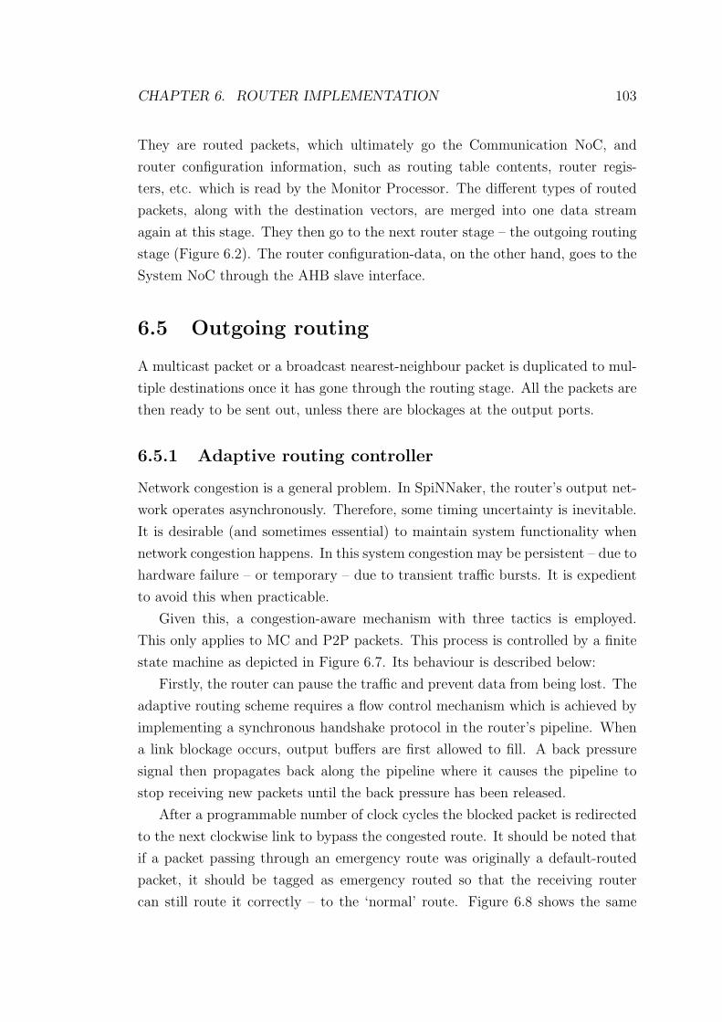
CHAPTER 6. ROUTER IMPLEMENTATION 103
They are routed packets, which ultimately go the Communication NoC, and
router configuration information, such as routing table contents, router regis-
ters, etc. which is read by the Monitor Processor. The different types of routed
packets, along with the destination vectors, are merged into one data stream
again at this stage. They then go to the next router stage – the outgoing routing
stage (Figure 6.2). The router configuration-data, on the other hand, goes to the
System NoC through the AHB slave interface.
6.5 Outgoing routing
A multicast packet or a broadcast nearest-neighbour packet is duplicated to mul-
tiple destinations once it has gone through the routing stage. All the packets are
then ready to be sent out, unless there are blockages at the output ports.
6.5.1 Adaptive routing controller
Network congestion is a general problem. In SpiNNaker, the router’s output net-
work operates asynchronously. Therefore, some timing uncertainty is inevitable.
It is desirable (and sometimes essential) to maintain system functionality when
network congestion happens. In this system congestion may be persistent – due to
hardware failure – or temporary – due to transient traffic bursts. It is expedient
to avoid this when practicable.
Given this, a congestion-aware mechanism with three tactics is employed.
This only applies to MC and P2P packets. This process is controlled by a finite
state machine as depicted in Figure 6.7. Its behaviour is described below:
Firstly, the router can pause the traffic and prevent data from being lost. The
adaptive routing scheme requires a flow control mechanism which is achieved by
implementing a synchronous handshake protocol in the router’s pipeline. When
a link blockage occurs, output buffers are first allowed to fill. A back pressure
signal then propagates back along the pipeline where it causes the pipeline to
stop receiving new packets until the back pressure has been released.
After a programmable number of clock cycles the blocked packet is redirected
to the next clockwise link to bypass the congested route. It should be noted that
if a packet passing through an emergency route was originally a default-routed
packet, it should be tagged as emergency routed so that the receiving router
can still route it correctly – to the ‘normal’ route. Figure 6.8 shows the same

CHAPTER 6. ROUTER IMPLEMENTATION 104
new packet arrived
packet departed
wait state 1
wait state 2 not expired
packet departed/no new packet
no new packet
/new packet arrived
/no new packetpacket departed
start
packet departed/new packet arrived
/new packet arrivedpacket departed
packet dropped/no new packet
packet departed/no new packet
/new packet arrivedpacket dropped
sending
wait state 2
wait state 1 expired
wait state 1 not expired
packet stalled
Figure 6.7: States of the adaptive routing controller
emergency routing example as Figure 5.5, which is described in section 5.4. In this
example, the emergency routed packet would go to node ‘X’ and further instead
of node ‘T’ if the router in node ‘D’ didn’t recognise that it has been redirected.
This emergency routing tag is not required by the P2P packet because every P2P
routing table has full route information of all P2P packets.
Lastly, if congestion persists the emergency route could also become congested.
If so, the emergency controller retries for a period and, if still unsuccessful, drops
the packet into the care of the local ‘Monitor’ Processor. The packet contents
may be recovered and ‘retry’ or ‘rerouting’ attempted in software if necessary.
The packet dropping mechanism allows the system to maintain a certain level
of Quality of Service (QoS). QoS is achievable in this parallel computer because
many neural applications are inherently fault-tolerant.
The adaptive routing mechanism can also help the system to quarantine a
permanent hardware failure: if a link is constantly invoking emergency routing,

CHAPTER 6. ROUTER IMPLEMENTATION 105
O
D
D TI
X
b c
a
E
Wrong destination
Figure 6.8: Redirecting an emergency routed packet back to the ‘normal’ route
the system may treat this as a permanent failure and could re-route packets to
avoid this link by reprogramming the routing tables.
6.5.2 Deadlock avoidance
The communications system has potential deadlock scenarios because of the pos-
sibility of circular dependencies between links. Because the neural events packet
is small, a ‘store-and-forward’ switching technique is used to achieve simpler im-
plementation: packets are passed around the asynchronous NoC in 4-bit flits but
these are de-serialised into complete packets when passing through the router to
make adaptive routing handling easier. The policy used here to prevent deadlocks
occurring is that no router can ever be prevented from issuing its output. Three
mechanisms are used to ensure this.
• Firstly, outputs have capacity detection so that the router knows whether
or not an output has the capacity to accept a packet.
• Secondly, adaptive routing is used, where possible, to avoid overloading a
blocked output.
• Finally, where adaptive routing fails (because, for example, the alternative
output is also blocked) the packet is ‘dropped’ to a router register, and the
Monitor Processor is informed to re-issue the packet.
The expectation is that the communications fabric will be lightly-loaded so
that blocked links are very rare. Where the operating system detects that this is
CHAPTER 6. ROUTER IMPLEMENTATION 106
not the case it will take measures to correct the problem by modifying routing
tables or migrating functionality to a different part of the system.
6.5.3 Adaptive routing timer
The adaptive routing mechanism makes its decision according to the local net-
work state information. An inappropriate rate of invoking the adaptive routing
mechanism will likely cause either a high packet loss rate or too long a traffic
delay. It is therefore necessary to make the waiting times, before invoking adap-
tive routing and before dropping a packet, adjustable. Two 8-bit counters are
employed for controlling the waiting times that are programmable across a wide
range of values, including zero and infinite wait times. To achieve a monotonic
increment of the intervals, the router employs a µ-law floating-point counter using
a binary pre-scaler and a loadable counter. Each 8-bit field is divided into a 4-bit
mantissa M [3:0] and a 4-bit exponent E[3:0]. The waiting time in clock cycles is
then given by:
wait = (M + 16− 24−E)× 2E, for E ≤ 4; (6.1)
wait = (M + 16)× 2E, for E > 4; (6.2)
M = E = 0000 gives a waiting time of zero. The wait time increases mono-
tonically with [E,M ]. ‘M = E = 1111’ is a special case and represents an infinite
wait time. This is useful for some neural simulations which do not tolerate spike
loss. To turn off the emergency routing, we can simply set the wait time to ‘zero’.
Turning off the emergency routing function is useful for some potential research
purposes. For example, when further exploring other possible network topologies,
the system organization can be changed to some different forms which do not have
emergency routes. Under such situation, the emergency routing function has to
be turned off to ensure the correctness of the routing.
6.6 Interfacing with the System NoC
The architecture of the System NoC was introduced in chapter 4. To realize the
system housekeeping features, the router acts as both an initiator and a target of
the System NoC. The System NoC provides a GALS interconnect across shared
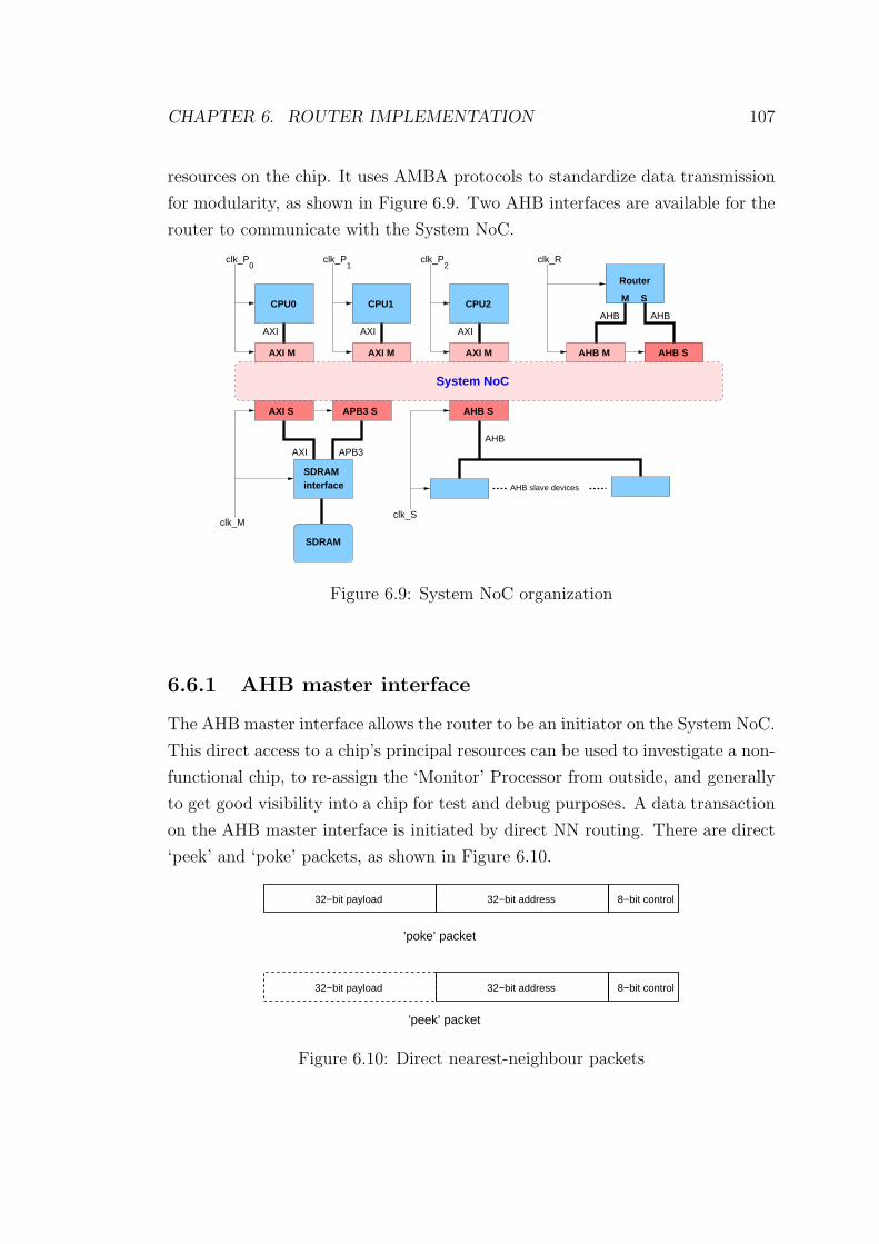
CHAPTER 6. ROUTER IMPLEMENTATION 107
resources on the chip. It uses AMBA protocols to standardize data transmission
for modularity, as shown in Figure 6.9. Two AHB interfaces are available for the
router to communicate with the System NoC.
0 1 2
CPU0 CPU1 CPU2
AXI M AXI M
AXI S APB3 S AHB S
AHB MAXI M
APB3
SM
Router
clk_P clk_P clk_R
AHB S
AHB
clk_M
clk_P
AHBAXI
interfaceSDRAM
SDRAM
AHB slave devices
clk_S
AXIAXIAXI
AHB
System NoC
Figure 6.9: System NoC organization
6.6.1 AHB master interface
The AHB master interface allows the router to be an initiator on the System NoC.
This direct access to a chip’s principal resources can be used to investigate a non-
functional chip, to re-assign the ‘Monitor’ Processor from outside, and generally
to get good visibility into a chip for test and debug purposes. A data transaction
on the AHB master interface is initiated by direct NN routing. There are direct
‘peek’ and ‘poke’ packets, as shown in Figure 6.10.
’peek’ packet
’poke’ packet
32−bit payload
32−bit payload 8−bit control
8−bit control32−bit address
32−bit address
Figure 6.10: Direct nearest-neighbour packets
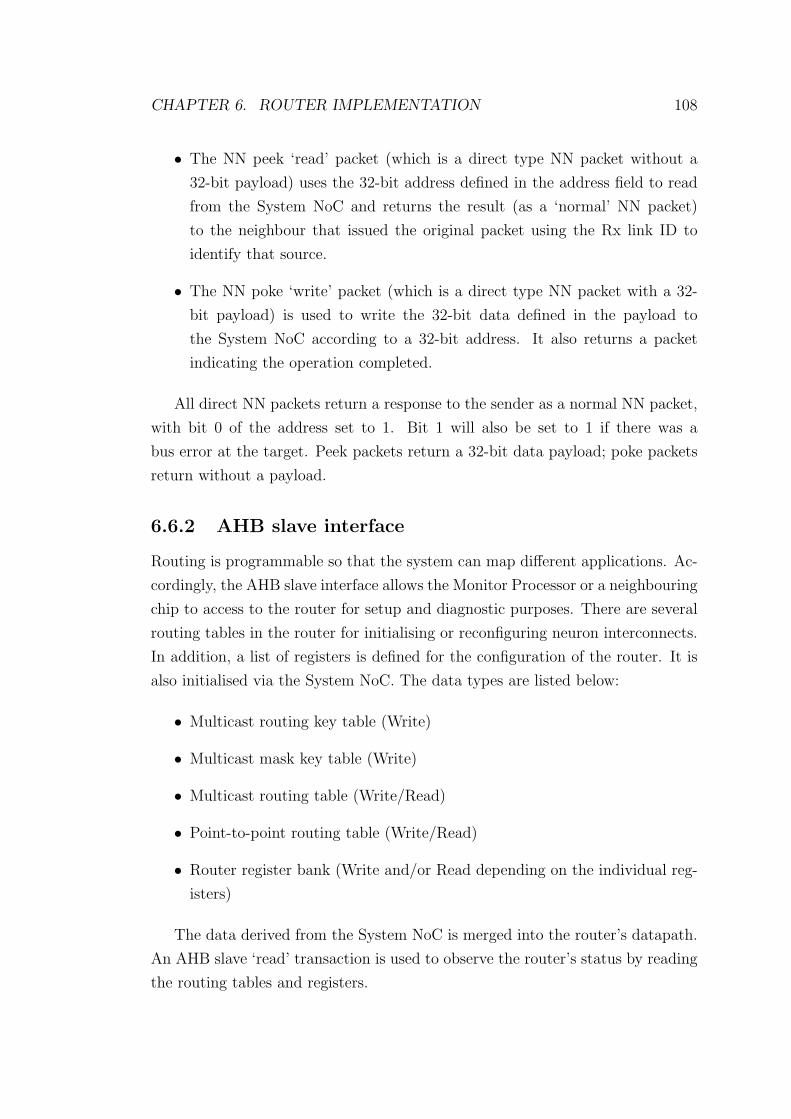
CHAPTER 6. ROUTER IMPLEMENTATION 108
• The NN peek ‘read’ packet (which is a direct type NN packet without a
32-bit payload) uses the 32-bit address defined in the address field to read
from the System NoC and returns the result (as a ‘normal’ NN packet)
to the neighbour that issued the original packet using the Rx link ID to
identify that source.
• The NN poke ‘write’ packet (which is a direct type NN packet with a 32-
bit payload) is used to write the 32-bit data defined in the payload to
the System NoC according to a 32-bit address. It also returns a packet
indicating the operation completed.
All direct NN packets return a response to the sender as a normal NN packet,
with bit 0 of the address set to 1. Bit 1 will also be set to 1 if there was a
bus error at the target. Peek packets return a 32-bit data payload; poke packets
return without a payload.
6.6.2 AHB slave interface
Routing is programmable so that the system can map different applications. Ac-
cordingly, the AHB slave interface allows the Monitor Processor or a neighbouring
chip to access to the router for setup and diagnostic purposes. There are several
routing tables in the router for initialising or reconfiguring neuron interconnects.
In addition, a list of registers is defined for the configuration of the router. It is
also initialised via the System NoC. The data types are listed below:
• Multicast routing key table (Write)
• Multicast mask key table (Write)
• Multicast routing table (Write/Read)
• Point-to-point routing table (Write/Read)
• Router register bank (Write and/or Read depending on the individual reg-
isters)
The data derived from the System NoC is merged into the router’s datapath.
An AHB slave ‘read’ transaction is used to observe the router’s status by reading
the routing tables and registers.
CHAPTER 6. ROUTER IMPLEMENTATION 109
6.7 Summary
This chapter introduced the design and implementation of the routing function,
which has a principal objective of performing multicast neural event routing, and
some other objectives including error handling, point-to-point routing, nearest-
neighbour routing, adaptive routing, etc. The router is divided into three main
functional stages. From the input to the output, they are the error handling
stage, the routing stage and the outgoing routing stage. Detailed design and op-
timization issues have been discussed to fulfill the special requirements of on-chip
multicast routing. The next chapter will present a elastic pipeline architecture,
which provides a feasible flow control mechanism to stall packets when adaptive
routing being performed. Because traffic flow in this router is sparse, elastic
pipelining achieves a better performance in terms of power and speed.
Chapter 7
Pipelining
This chapter discusses the transaction signalling inside the router’s pipeline, de-
signed to facilitate data transmission in the asynchronous Communication NoC.
The router is implemented synchronously enabling use of a typical VLSI design
flow. A synchronous handshake protocol is proposed in the router’s pipeline to
support a flow-control mechanism, which is required by the adaptive routing,
elastic buffering and power saving.
7.1 Introduction
Increasing clock frequency has worsened clock skew problems faced by large-scale
synchronous VLSI design. In addition, some large, complex designs may require
the integration of fully-designed and tested IP blocks on a single die for the benefit
of design reuse. However, these IP blocks are usually designed with different clock
frequencies, and this calls for special integration solutions. The GALS paradigm
is a system-level interconnection approach which offers a promising solution to
these problems [Cha84]. A GALS system uses asynchronous channels to connect
synchronous function-blocks. Clock domains are decoupled by the channels. This
brings many merits for large-scale integration:
• Shorter prototype procedure: The interfaces between the synchronous sub-
modules and the asynchronous interconnects are usually standardized for
design modularization.
• Simplification of timing closure: Sub-circuits are synchronized by local
clocks. Fixing clock skew problems becomes easier.
110

CHAPTER 7. PIPELINING 111
• Power saving: The global clock tree, which required a large power driving,
no longer exists. Synchronous sub-modules have their own power supply
voltages which can be locally adjusted or even shut down [MHK+99].
7.2 The GALS approach for inter-neuron com-
munication
As mentioned above, the GALS approach has many advantages for the implemen-
tation of a large-scale parallel system. In addition, there are three special reasons
for the GALS infrastructure to be highly suitable for the SpiNNaker system:
• A neural spike is an asynchronous event. It can be simply be routed through
to the next chip and never needs to be synchronized to a local processor.
• The SpiNNaker system is a universal neural network simulation platform
that requires flexibility in the chip organization. Asynchronous interconnect
decouples the clock domains between and within the chips, and helps make
the system scalable. As a result, the system can effectively model different
scales of neural network for different purposes, ranging from a few thousand
to billions of neurons.
• A neuron has a typical fan-out of around 1,000. Conventional synchronous
buses, which usually support one-to-one communication, have great diffi-
culty in maintaining adequate bandwidth for such a high density of connec-
tions.
7.3 Synchronous latency-insensitive pipeline
The SpiNNaker router is implemented as a synchronous pipelined module with
asynchronous links [PFT+07]. Compared to an asynchronous router it is easier to
design using a standard VLSI design flow and it is easier to incorporate clocked
memory blocks such as CAMs and RAMs. Normal traffic is expected to be sparse,
but there may be arbitrary output delays, so rapid throughput but buffering ca-
pacity is desired by the application. The router’s synchronous pipeline is designed
to be elastic so that it provides flexibility in flow control and can make effective
use of the delay-insensitive feature of the GALS NoC.
CHAPTER 7. PIPELINING 112
7.3.1 Synchronous handshake pipeline
Although much of the pipeline activity is conventionally synchronous there are
some reasons to deviate from a simple model:
• The spike rate for the great majority of neurons is expected to be low – just
a few Hz. As a result, there will be many pipeline ‘bubbles’ between valid
packets which will cause power wastage if they pass through a conventional
pipeline, especially when the pipeline contains power-hungry blocks such
as look-up RAMs and CAMs. It is desirable to deactivate pipeline stages
when data is not valid.
• There can be more than one request to the datapath issued in the same
clock cycle. When this happens, the interface with the highest priority will
occupy the datapath and the other(s) will be stalled. The data is arbitrated
at the router’s packet arbitration stage introduced in chapter 6.
• The adaptive routing mechanism may need to stall the pipeline so that the
router can find an alternative path for a congested packet.
Following the above analysis, a router with an elastic pipeline is implemented
so that the design is tolerant of the variations of asynchronous data transfer rates
in the GALS system.
An elastic pipeline is also called a latency-insensitive (LI) design. The stall
and propagation of data in a LI pipeline is usually controlled by transaction
signalling; this particular one uses two wires to implement a handshake protocol
that is similar to the asynchronous handshake protocol: ‘valid’ for the forward
flow control, and ‘stall’ for backpressure signalling.
There are valid and invalid data passing through the pipeline, which are called
tokens and bubbles. A pipeline stage is activated if a token arrives. The valid
bit is latched at that stage to indicate that the stage is full. When the pipeline is
full, the stall signal is propagated backwards up the pipeline until it reaches the
front of the pipeline where it is propagated to the data synchronizer connected to
the asynchronous Communication NoC. The data latches are stopped by the stall
signals and hold their current data. The cause of a stall signal could be either
backpressure from the output buffer or an AHB request claiming priority.
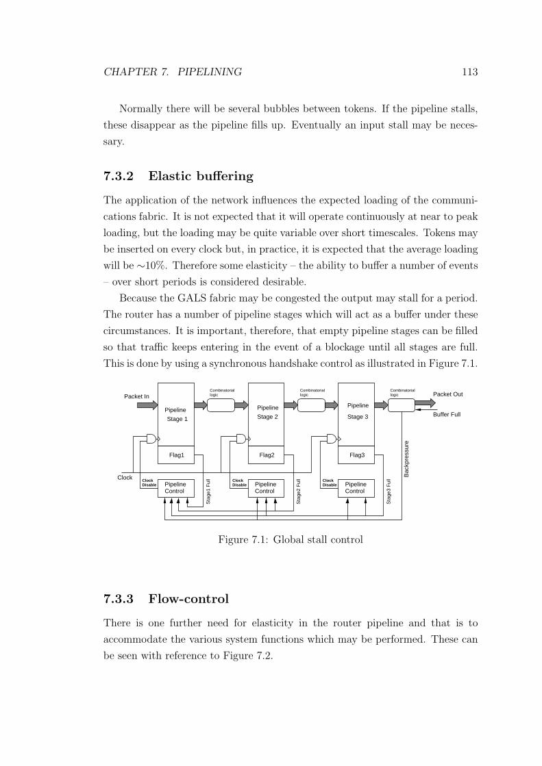
CHAPTER 7. PIPELINING 113
Normally there will be several bubbles between tokens. If the pipeline stalls,
these disappear as the pipeline fills up. Eventually an input stall may be neces-
sary.
7.3.2 Elastic buffering
The application of the network influences the expected loading of the communi-
cations fabric. It is not expected that it will operate continuously at near to peak
loading, but the loading may be quite variable over short timescales. Tokens may
be inserted on every clock but, in practice, it is expected that the average loading
will be ∼10%. Therefore some elasticity – the ability to buffer a number of events
– over short periods is considered desirable.
Because the GALS fabric may be congested the output may stall for a period.
The router has a number of pipeline stages which will act as a buffer under these
circumstances. It is important, therefore, that empty pipeline stages can be filled
so that traffic keeps entering in the event of a blockage until all stages are full.
This is done by using a synchronous handshake control as illustrated in Figure 7.1.
Stage 1
Pipeline
PipelineControl
Sta
ge1
Ful
l
Packet In
ClockDisableDisable Pipeline
Control ControlPipeline
Flag3Flag2Flag1
Pipeline
Stage 3
PipelineB
ackp
ress
ure
Sta
ge2
Ful
lClockDisableClockClock
Packet Out
Buffer Full
Sta
ge3
Ful
l
Stage 2
logicCombinatorial
logicCombinatorial Combinatorial
logic
Figure 7.1: Global stall control
7.3.3 Flow-control
There is one further need for elasticity in the router pipeline and that is to
accommodate the various system functions which may be performed. These can
be seen with reference to Figure 7.2.

CHAPTER 7. PIPELINING 114
AR
BIT
ER
From Packet Checker
CAM Test KeyCAM Mask WriteCAM Key WriteMC RAM Write
P2P RAM ReadCAM Hits ReadMC RAM Read
NN packet
Direct
Error Dump
AHB M AHB S
System NoC
Bank
Register
NN packetNormal
P2P packetMC packet
Normal NN packet
Normal NN Routing
MC Routing
P2P Routing
To Emergency Router
MC packet
P2P packet
NN packet
Route
Routing Stage
P2P packetMC packet
NN packetError packet
P2P RAM Write
Figure 7.2: Data flows to the router
• Some packets are diverted onto the System NoC. These ‘disappear’ from
the packet stream whilst they perform read or write operations. Responses
are, however, reintroduced by arbitrating into (and, possibly, stalling) the
normal packet flow.
• Programming data used to set up routing tables is sourced from the System
NoC. For reasons of size and speed the routing tables are in standard, single-
port RAMs; it is therefore necessary to arbitrate programming packets into
the pipeline. For test purposes it is also possible to request reads from these
RAMs where data is returned to the System NoC.
• Writing the multicast CAM also uses pipelined packets. In practice, CAM
writing causes a longer stall due to the CAM implementation, but this will
not normally occur during active simulations.
7.3.4 Clock gating
Power consumption is of great concern in the design of very large-scale com-
putation networks. Even a slight waste of power on an individual sub-module
can cause a large increase of power of the whole system and limit the system’s
scalability.
The power consumption of VLSI circuits is calculated by the function:
P = Ps + Pi + Pl (7.1)
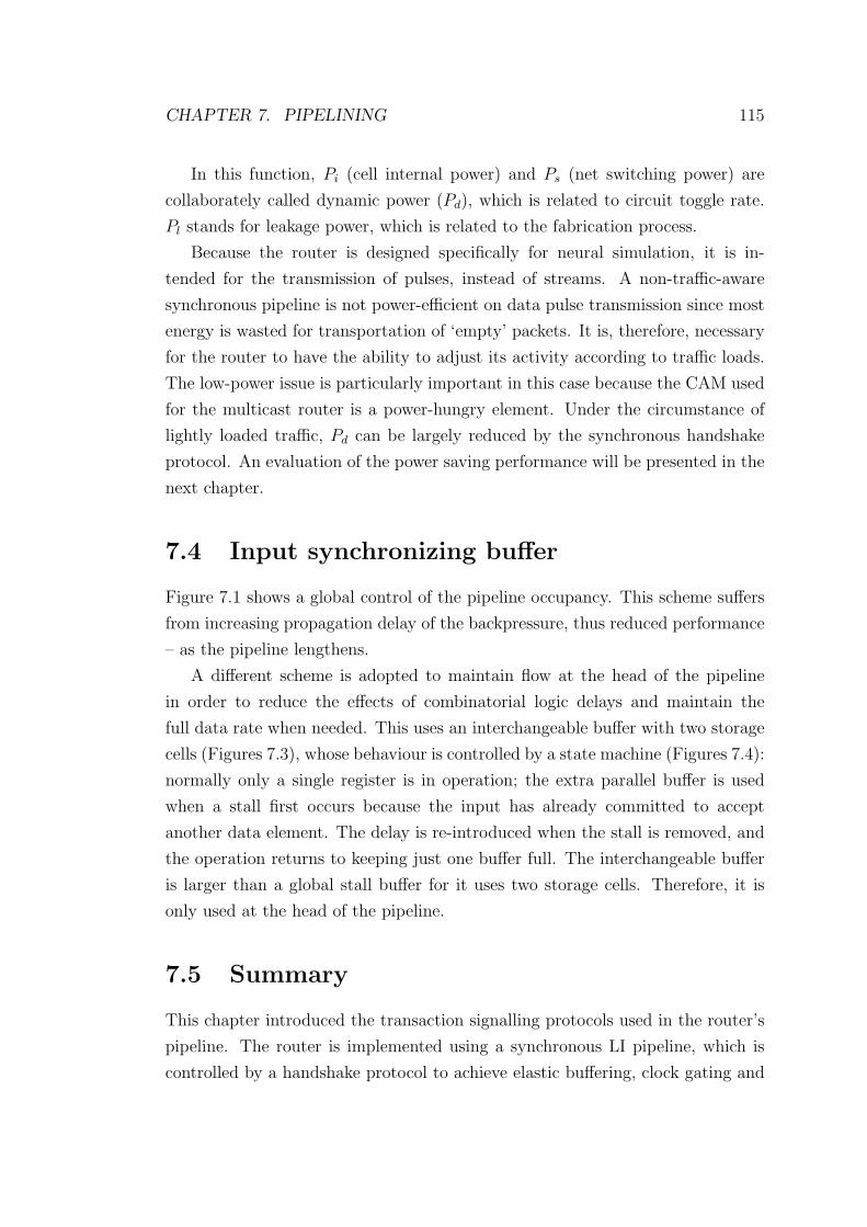
CHAPTER 7. PIPELINING 115
In this function, Pi (cell internal power) and Ps (net switching power) are
collaborately called dynamic power (Pd), which is related to circuit toggle rate.
Pl stands for leakage power, which is related to the fabrication process.
Because the router is designed specifically for neural simulation, it is in-
tended for the transmission of pulses, instead of streams. A non-traffic-aware
synchronous pipeline is not power-efficient on data pulse transmission since most
energy is wasted for transportation of ‘empty’ packets. It is, therefore, necessary
for the router to have the ability to adjust its activity according to traffic loads.
The low-power issue is particularly important in this case because the CAM used
for the multicast router is a power-hungry element. Under the circumstance of
lightly loaded traffic, Pd can be largely reduced by the synchronous handshake
protocol. An evaluation of the power saving performance will be presented in the
next chapter.
7.4 Input synchronizing buffer
Figure 7.1 shows a global control of the pipeline occupancy. This scheme suffers
from increasing propagation delay of the backpressure, thus reduced performance
– as the pipeline lengthens.
A different scheme is adopted to maintain flow at the head of the pipeline
in order to reduce the effects of combinatorial logic delays and maintain the
full data rate when needed. This uses an interchangeable buffer with two storage
cells (Figures 7.3), whose behaviour is controlled by a state machine (Figures 7.4):
normally only a single register is in operation; the extra parallel buffer is used
when a stall first occurs because the input has already committed to accept
another data element. The delay is re-introduced when the stall is removed, and
the operation returns to keeping just one buffer full. The interchangeable buffer
is larger than a global stall buffer for it uses two storage cells. Therefore, it is
only used at the head of the pipeline.
7.5 Summary
This chapter introduced the transaction signalling protocols used in the router’s
pipeline. The router is implemented using a synchronous LI pipeline, which is
controlled by a handshake protocol to achieve elastic buffering, clock gating and
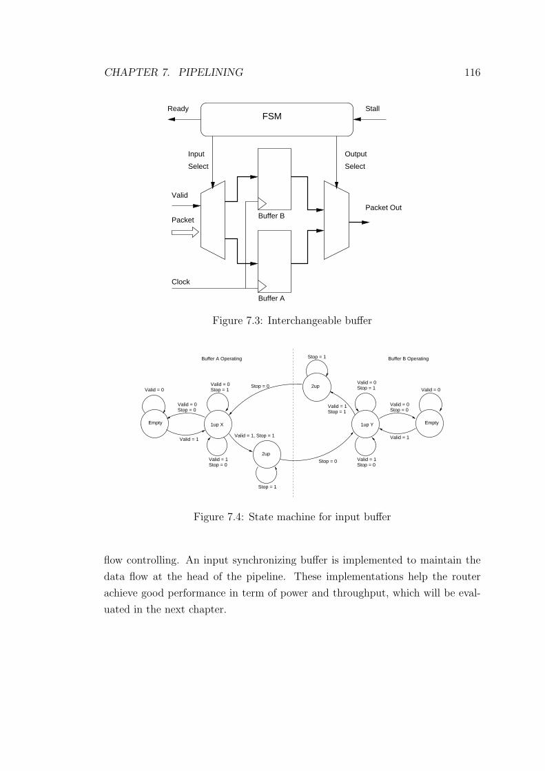
CHAPTER 7. PIPELINING 116
Valid
Ready
Clock
FSM
Input
Select
Packet
Select
Output
Buffer B
Buffer A
Packet Out
Stall
Figure 7.3: Interchangeable buffer
1up X 1up Y
2up
2up
Buffer B OperatingBuffer A Operating
Empty
Valid = 0Stop = 0
Valid = 1
Empty
Valid = 0 Stop = 1Valid = 0
Valid = 1Stop = 0
Valid = 1, Stop = 1
Stop = 1
Stop = 0
Stop = 0
Stop = 1
Valid = 1Stop = 1
Valid = 0Stop = 1
Valid = 1Stop = 0
Stop = 0Valid = 0
Valid = 1
Valid = 0
Figure 7.4: State machine for input buffer
flow controlling. An input synchronizing buffer is implemented to maintain the
data flow at the head of the pipeline. These implementations help the router
achieve good performance in term of power and throughput, which will be eval-
uated in the next chapter.
Chapter 8
Evaluation
Chapter 4 proposed the communication scheme of a router in the context of the
SpiNNaker system. Chapter 5 discussed the router’s routing requirements and
design considerations. The issues of its implementations were then introduced
in chapter 6 and chapter 7. This chapter presents functional validations and
performance evaluations of the router through simulations.
The validation and evaluation actions include:
• post-synthesis and post-layout analysis of the router giving concrete evi-
dence to show that the design of the router fulfills the timing and power
requirements.
• the router test bench written in Verilog is used to verify the router’s basic
functions defined in chapter 5.
• system-level simulation of SpiNNaker validating the router’s functions in
‘real-world’ neural modelling.
• measurement of the router’s packet loss ratio under different network block-
age rates and waiting times showing the effectiveness of the adaptive routing
algorithm.
• system-level simulation of SpiNNaker to measure the router’s ability to
reduce the system’s packet loss ratio in a networked environment.
• post-synthesis measurement of the router’s power performance under dif-
ferent traffic loads showing the effectiveness of the elastic pipeline design in
reducing power consumption.
117
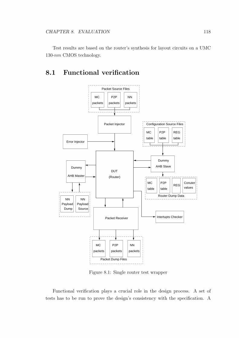
CHAPTER 8. EVALUATION 118
Test results are based on the router’s synthesis for layout circuits on a UMC
130-nm CMOS technology.
8.1 Functional verification
table
Packet Source Files
Configuration Source FilesPacket Injector
Packet Dump Files
Dummy
Payload
NN
Payload
Dump
NN
Source
AHB Master
Packet Receiver Intertupts Checker
Dummy
AHB Slave
MC
table tableError Injector
P2P
MC
packets
P2P REG
MC P2P
table tableREG
Router Dump Data
Conuter
values
DUT
(Router)
packets
P2P
packetspackets
NN
packets
MC
packets
NN
Figure 8.1: Single router test wrapper
Functional verification plays a crucial role in the design process. A set of
tests has to be run to prove the design’s consistency with the specification. A
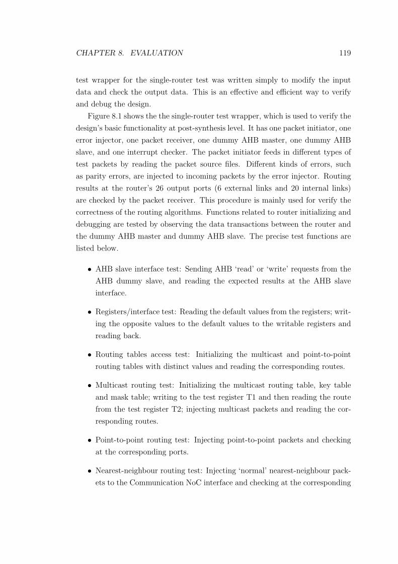
CHAPTER 8. EVALUATION 119
test wrapper for the single-router test was written simply to modify the input
data and check the output data. This is an effective and efficient way to verify
and debug the design.
Figure 8.1 shows the the single-router test wrapper, which is used to verify the
design’s basic functionality at post-synthesis level. It has one packet initiator, one
error injector, one packet receiver, one dummy AHB master, one dummy AHB
slave, and one interrupt checker. The packet initiator feeds in different types of
test packets by reading the packet source files. Different kinds of errors, such
as parity errors, are injected to incoming packets by the error injector. Routing
results at the router’s 26 output ports (6 external links and 20 internal links)
are checked by the packet receiver. This procedure is mainly used for verify the
correctness of the routing algorithms. Functions related to router initializing and
debugging are tested by observing the data transactions between the router and
the dummy AHB master and dummy AHB slave. The precise test functions are
listed below.
• AHB slave interface test: Sending AHB ‘read’ or ‘write’ requests from the
AHB dummy slave, and reading the expected results at the AHB slave
interface.
• Registers/interface test: Reading the default values from the registers; writ-
ing the opposite values to the default values to the writable registers and
reading back.
• Routing tables access test: Initializing the multicast and point-to-point
routing tables with distinct values and reading the corresponding routes.
• Multicast routing test: Initializing the multicast routing table, key table
and mask table; writing to the test register T1 and then reading the route
from the test register T2; injecting multicast packets and reading the cor-
responding routes.
• Point-to-point routing test: Injecting point-to-point packets and checking
at the corresponding ports.
• Nearest-neighbour routing test: Injecting ‘normal’ nearest-neighbour pack-
ets to the Communication NoC interface and checking at the corresponding
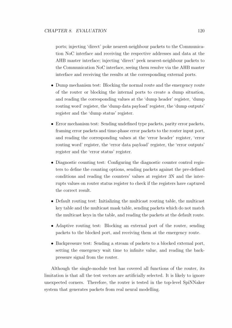
CHAPTER 8. EVALUATION 120
ports; injecting ‘direct’ poke nearest-neighbour packets to the Communica-
tion NoC interface and receiving the respective addresses and data at the
AHB master interface; injecting ‘direct’ peek nearest-neighbour packets to
the Communication NoC interface, seeing them resolve via the AHB master
interface and receiving the results at the corresponding external ports.
• Dump mechanism test: Blocking the normal route and the emergency route
of the router or blocking the internal ports to create a dump situation,
and reading the corresponding values at the ‘dump header’ register, ‘dump
routing word’ register, the ‘dump data payload’ register, the ‘dump outputs’
register and the ‘dump status’ register.
• Error mechanism test: Sending undefined type packets, parity error packets,
framing error packets and time-phase error packets to the router input port,
and reading the corresponding values at the ‘error header’ register, ‘error
routing word’ register, the ‘error data payload’ register, the ‘error outputs’
register and the ‘error status’ register.
• Diagnostic counting test: Configuring the diagnostic counter control regis-
ters to define the counting options, sending packets against the pre-defined
conditions and reading the counters’ values at register 3N and the inter-
rupts values on router status register to check if the registers have captured
the correct result.
• Default routing test: Initializing the multicast routing table, the multicast
key table and the multicast mask table, sending packets which do not match
the multicast keys in the table, and reading the packets at the default route.
• Adaptive routing test: Blocking an external port of the router, sending
packets to the blocked port, and receiving them at the emergency route.
• Backpressure test: Sending a stream of packets to a blocked external port,
setting the emergency wait time to infinite value, and reading the back-
pressure signal from the router.
Although the single-module test has covered all functions of the router, its
limitation is that all the test vectors are artificially selected. It is likely to ignore
unexpected corners. Therefore, the router is tested in the top-level SpiNNaker
system that generates packets from real neural modelling.
CHAPTER 8. EVALUATION 121
8.2 Multi-chip SpiNNaker system simulation
A system-level simulation can generate more realistic and random test vectors for
the sub-modules. In the test of the router, several modules are put in a networked
environment running spiking neural modelling, where the routers can send packets
to each other. To perform a fast simulation, a four-chip network was created as
shown in Figure 8.2. The chips are linked into a triangular mesh, thus they
form the minimum scale of network which can reflect the network topology of the
SpiNNaker system. Each chip contains a router and two ARM 968 processing
cores, which is also the minimum requirement for a chip: one ARM processor
serves as the Monitor Processor for system management, the other serves as the
fascicle processor for neural computing. The chip modules are written in Verilog
RTL code.
Router
Router Router
M
M
Chip (0,1) Chip (1,1)
Chip (0,0) Chip (1,0)
Router
M FF
MF F
Neuron parameters
Synaptic weights and connects
Rec
eive
d pa
ckes
dum
p fil
e
Synaptic weights and connects
Neuron parameters
Rec
eive
d pa
ckes
dum
p fil
eR
ecei
ved
pack
es d
ump
file
Neuron parameters
Synaptic weights and connects
Neuron parameters
Synaptic weights and connects
Rec
eive
d pa
ckes
dum
p fil
e
Figure 8.2: Four-chip test wrapper
CHAPTER 8. EVALUATION 122
The simulation procedure is first to load ARM code into the ROMs and Sys-
tem RAMs, thus initializing the system. The Monitor Processor on each chip
then generates routing tables for each router. Neural networks are mapped on
the fascicle processors with varying numbers of neurons and random connections.
Neurons are modelled using the Izhikevich model [Izh03], which is to be used
as a major model in the actual platform. When the simulation starts, fascicle
processors randomly generate neural spikes to local processors or to other chips.
The simulation records the output packets sent from each processor. Post simu-
lation, all packets will eventually be routed to the fascicle processors, or dropped
to the Monitor Processors due to some error such as end-of-packet error or parity
error. The packets received at each fascicle processor and Monitor Processor are
recorded in fascicle processor output files and Monitor Processor output files.
A simulation of 120 ms platform running time was performed, lasting about
50 hours on a Linux workstation. Each fascicle processor maintained 60 spiking
neurons, so the total number of neurons simulated was 240. Each neuron was
connected to 3 other neurons on average and as the firing rate of a neuron is
between 1 Hz and 1000 Hz, the total number of spikes during the simulation was
between ∼30 and 28,800. The router’s waiting time before dropping a packet was
set to ‘infinite’ to ensure the router does not drop any packet when congestion
happens. Finally, the packet record files for the sent packets and received packets
were then compared. The result proved that the routers correctly route the
packets as anticipated.
8.3 Optimum buffer length
A buffer is placed at each output port of the router to maintain the throughput
under transient congestion. The buffer, which works as a FIFO (first in, first
out) memory, is implemented using registers. As implementation cost and power
dissipation are important factors to be considered when designing an on-chip
router, it is necessary to derive the optimum length of the buffer to choose a
good trade-off between performance and area/power.
In order to understand the buffer length’s impact on the on-chip resources,
the SpiNNaker router was synthesized with different buffer sizes using the UMC
130-nm technology. Figure 8.3 shows the area of the router as a function of buffer
size. The area of the router is represented by gate number, while the buffer size
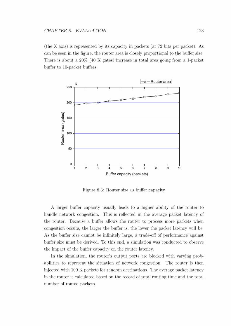
CHAPTER 8. EVALUATION 123
(the X axis) is represented by its capacity in packets (at 72 bits per packet). As
can be seen in the figure, the router area is closely proportional to the buffer size.
There is about a 20% (40 K gates) increase in total area going from a 1-packet
buffer to 10-packet buffers.
1 2 3 4 5 6 7 8 9 100
50
100
150
200
250
Rou
ter a
rea
(gat
es)
Buffer capacity (packets)
Router areaK
Figure 8.3: Router size vs buffer capacity
A larger buffer capacity usually leads to a higher ability of the router to
handle network congestion. This is reflected in the average packet latency of
the router. Because a buffer allows the router to process more packets when
congestion occurs, the larger the buffer is, the lower the packet latency will be.
As the buffer size cannot be infinitely large, a trade-off of performance against
buffer size must be derived. To this end, a simulation was conducted to observe
the impact of the buffer capacity on the router latency.
In the simulation, the router’s output ports are blocked with varying prob-
abilities to represent the situation of network congestion. The router is then
injected with 100 K packets for random destinations. The average packet latency
in the router is calculated based on the record of total routing time and the total
number of routed packets.
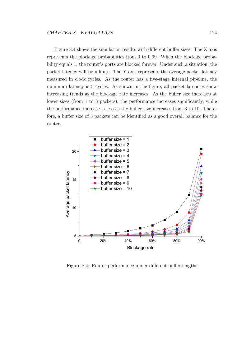
CHAPTER 8. EVALUATION 124
Figure 8.4 shows the simulation results with different buffer sizes. The X axis
represents the blockage probabilities from 0 to 0.99. When the blockage proba-
bility equals 1, the router’s ports are blocked forever. Under such a situation, the
packet latency will be infinite. The Y axis represents the average packet latency
measured in clock cycles. As the router has a five-stage internal pipeline, the
minimum latency is 5 cycles. As shown in the figure, all packet latencies show
increasing trends as the blockage rate increases. As the buffer size increases at
lower sizes (from 1 to 3 packets), the performance increases significantly, while
the performance increase is less as the buffer size increases from 3 to 10. There-
fore, a buffer size of 3 packets can be identified as a good overall balance for the
router.
0 20% 40% 60% 80% 99%5
10
15
20
Ave
rage
pac
ket l
aten
cy
Blockage rate
buffer size = 1 buffer size = 2 buffer size = 3 buffer size = 4 buffer size = 5 buffer size = 6 buffer size = 7 buffer size = 8 buffer size = 9 buffer size = 10
Figure 8.4: Router performance under different buffer lengths
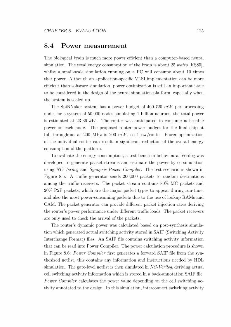
CHAPTER 8. EVALUATION 125
8.4 Power measurement
The biological brain is much more power efficient than a computer-based neural
simulation. The total energy consumption of the brain is about 25 watts [KS85],
whilst a small-scale simulation running on a PC will consume about 10 times
that power. Although an application-specific VLSI implementation can be more
efficient than software simulation, power optimization is still an important issue
to be considered in the design of the neural simulation platform, especially when
the system is scaled up.
The SpiNNaker system has a power budget of 460-720 mW per processing
node, for a system of 50,000 nodes simulating 1 billion neurons, the total power
is estimated at 23-36 kW . The router was anticipated to consume noticeable
power on each node. The proposed router power budget for the final chip at
full throughput at 200 MHz is 200 mW , so 1 nJ/route. Power optimization
of the individual router can result in significant reduction of the overall energy
consumption of the platform.
To evaluate the energy consumption, a test-bench in behavioural Verilog was
developed to generate packet streams and estimate the power by co-simulation
using NC-Verilog and Synopsis Power Compiler. The test scenario is shown in
Figure 8.5. A traffic generator sends 200,000 packets to random destinations
among the traffic receivers. The packet stream contains 80% MC packets and
20% P2P packets, which are the major packet types to appear during run-time,
and also the most power-consuming packets due to the use of lookup RAMs and
CAM. The packet generator can provide different packet injection rates deriving
the router’s power performance under different traffic loads. The packet receivers
are only used to check the arrival of the packets.
The router’s dynamic power was calculated based on post-synthesis simula-
tion which generated actual switching activity stored in SAIF (Switching Activity
Interchange Format) files. An SAIF file contains switching activity information
that can be read into Power Compiler. The power calculation procedure is shown
in Figure 8.6: Power Compiler first generates a forward SAIF file from the syn-
thesized netlist, this contains any information and instructions needed by HDL
simulation. The gate-level netlist is then simulated in NC-Verilog, deriving actual
cell switching activity information which is stored in a back-annotation SAIF file.
Power Compiler calculates the power value depending on the cell switching ac-
tivity annotated to the design. In this simulation, interconnect switching activity
CHAPTER 8. EVALUATION 126
Router
Packet Generator
Packet
MC
80%
Packet
P2P
20%
Packet Receiver
Figure 8.5: The Scenario of dynamic power estimation
is ignored.
The simulation is carried out under typical conditions on the UMC 130-nm
CMOS technology. The dynamic power consumption has been calculated on a
router with 1024 CAM entries, a number that will be used in the final chip.
The router was working under different traffic loads from a 100% traffic load
to 10% of its maximum throughput. As shown in Figure 8.7, the power usage
decreases when the traffic load drops: Under 100% packet load, the overall power
consumption is 64 mW . However, when the packet load drops to 10%, the overall
power is only 27 mW resulting in roughly 50% power saving.
The power measurement also varies significantly in each sub-unit of the router,
except the P2P router and its lookup RAM, whose power consumption is not
affected by the multicast traffic. Another simulation was conducted to illustrate
the major power reduction is from the CAM when traffic load is low. To emulate
a run-time situation, the injected packets in this test are only MC packets. As
shown in Figure 8.8, the 1024-entry multicast CAM occupies a great proportion
of the router’s overall power budget. The 1024-entry CAM consumes over 50%
(31 mW ) of the total power. This result is derived under the circumstance where

CHAPTER 8. EVALUATION 127
RTL DesignTechnology
Library
Forward SAIF File Gate Level Netlist
Gate Level Simulation
Backward SAIF File
NC−Verilog
BackAnnotation
Report Power
Power Compiler
Design Compiler
Figure 8.6: Power estimation flow through gate level simulation
a valid packet is inserted on every clock.
In practice, it is expected that the average loading of each router will be
below 10% although the traffic load is expected to be non-uniform and change
dynamically. It is important, therefore, that any unnecessary circuit switching
of the power-hungry CAM is eliminated so that its dynamic power consumption
is reduced to a minimum. This is done using pipeline control which enables a
pipeline register only when a token has arrived. This traffic-aware pipeline control
unit eliminates unnecessary gate transitions caused by the data ‘bubbles’, and
consequently reduces dynamic power consumption [PFT+07]. By this means,
the power cost is made proportional to the packet load. Since the router is
lightly loaded at most times, the overall energy consumption during run time
is significantly reduced. The power saving achieved on all of the token-based
pipelined units where the CAM’s power drops significantly from 31 mW to 3 mW ,
is shown in Figure 8.9.
This result also indicates that the reduction in the number of CAM entries
by employing hierarchical routing and default routing also has a great impact on
power saving.
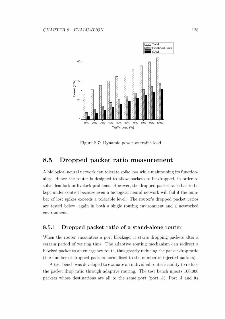
CHAPTER 8. EVALUATION 128
10% 20% 30% 40% 50% 60% 70% 80% 90% 100%0
20
40
60
Pow
er (m
W)
Traffic Load (%)
Total Pipelined units CAM
Figure 8.7: Dynamic power vs traffic load
8.5 Dropped packet ratio measurement
A biological neural network can tolerate spike loss while maintaining its function-
ality. Hence the router is designed to allow packets to be dropped, in order to
solve deadlock or livelock problems. However, the dropped packet ratio has to be
kept under control because even a biological neural network will fail if the num-
ber of lost spikes exceeds a tolerable level. The router’s dropped packet ratios
are tested below, again in both a single routing environment and a networked
environment.
8.5.1 Dropped packet ratio of a stand-alone router
When the router encounters a port blockage, it starts dropping packets after a
certain period of waiting time. The adaptive routing mechanism can redirect a
blocked packet to an emergency route, thus greatly reducing the packet drop ratio
(the number of dropped packets normalised to the number of injected packets).
A test bench was developed to evaluate an individual router’s ability to reduce
the packet drop ratio through adaptive routing. The test bench injects 100,000
packets whose destinations are all to the same port (port A). Port A and its
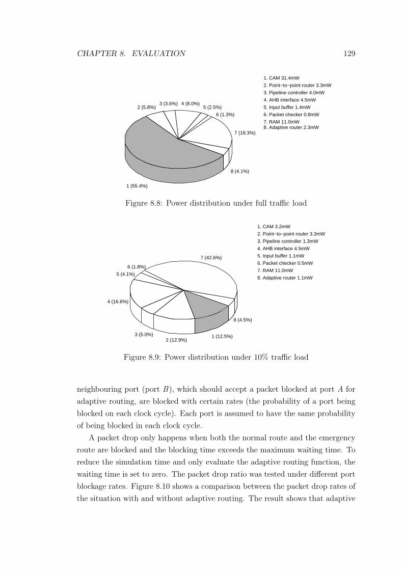
CHAPTER 8. EVALUATION 129
7 (19.3%)
8 (4.1%)
8. Adaptive router 2.3mW7. RAM 11.0mW
6. Packet checker 0.8mW
5. Input buffer 1.4mW
4. AHB interface 4.5mW
3. Pipeline controller 4.0mW
1. CAM 31.4mW
1 (55.4%)
4 (8.0%)
6 (1.3%)
5 (2.5%)3 (3.6%)
2 (5.8%)
2. Point−to−point router 3.3mW
Figure 8.8: Power distribution under full traffic load
1 (12.5%)2 (12.9%)
8 (4.5%)
7 (42.6%)
6 (1.8%)
5 (4.1%)
4 (16.6%)
1. CAM 3.2mW
2. Point−to−point router 3.3mW
3. Pipeline controller 1.3mW
4. AHB interface 4.5mW
5. Input buffer 1.1mW
6. Packet checker 0.5mW
7. RAM 11.0mW
8. Adaptive router 1.1mW
3 (5.0%)
Figure 8.9: Power distribution under 10% traffic load
neighbouring port (port B), which should accept a packet blocked at port A for
adaptive routing, are blocked with certain rates (the probability of a port being
blocked on each clock cycle). Each port is assumed to have the same probability
of being blocked in each clock cycle.
A packet drop only happens when both the normal route and the emergency
route are blocked and the blocking time exceeds the maximum waiting time. To
reduce the simulation time and only evaluate the adaptive routing function, the
waiting time is set to zero. The packet drop ratio was tested under different port
blockage rates. Figure 8.10 shows a comparison between the packet drop rates of
the situation with and without adaptive routing. The result shows that adaptive
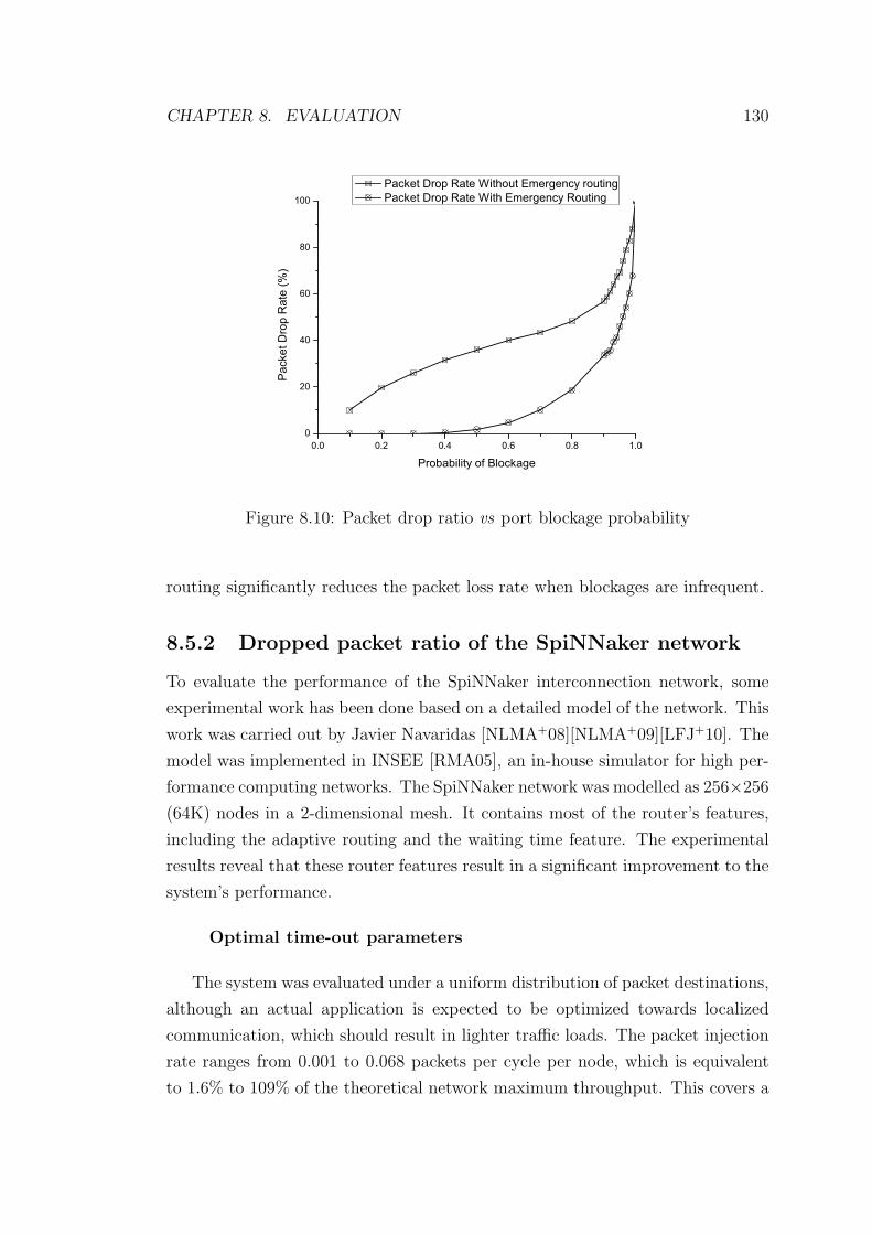
CHAPTER 8. EVALUATION 130
0.0 0.2 0.4 0.6 0.8 1.00
20
40
60
80
100
Pac
ket D
rop
Rat
e (%
)
Probability of Blockage
Packet Drop Rate Without Emergency routing Packet Drop Rate With Emergency Routing
Figure 8.10: Packet drop ratio vs port blockage probability
routing significantly reduces the packet loss rate when blockages are infrequent.
8.5.2 Dropped packet ratio of the SpiNNaker network
To evaluate the performance of the SpiNNaker interconnection network, some
experimental work has been done based on a detailed model of the network. This
work was carried out by Javier Navaridas [NLMA+08][NLMA+09][LFJ+10]. The
model was implemented in INSEE [RMA05], an in-house simulator for high per-
formance computing networks. The SpiNNaker network was modelled as 256×256
(64K) nodes in a 2-dimensional mesh. It contains most of the router’s features,
including the adaptive routing and the waiting time feature. The experimental
results reveal that these router features result in a significant improvement to the
system’s performance.
Optimal time-out parameters
The system was evaluated under a uniform distribution of packet destinations,
although an actual application is expected to be optimized towards localized
communication, which should result in lighter traffic loads. The packet injection
rate ranges from 0.001 to 0.068 packets per cycle per node, which is equivalent
to 1.6% to 109% of the theoretical network maximum throughput. This covers a
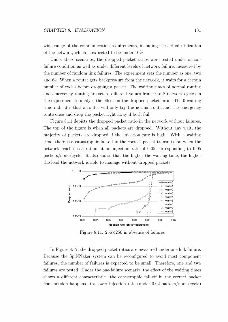
CHAPTER 8. EVALUATION 131
wide range of the communication requirements, including the actual utilization
of the network, which is expected to be under 10%.
Under these scenarios, the dropped packet ratios were tested under a non-
failure condition as well as under different levels of network failure, measured by
the number of random link failures. The experiment sets the number as one, two
and 64. When a router gets backpressure from the network, it waits for a certain
number of cycles before dropping a packet. The waiting times of normal routing
and emergency routing are set to different values from 0 to 8 network cycles in
the experiment to analyse the effect on the dropped packet ratio. The 0 waiting
time indicates that a router will only try the normal route and the emergency
route once and drop the packet right away if both fail.
Figure 8.11 depicts the dropped packet ratio in the network without failures.
The top of the figure is when all packets are dropped. Without any wait, the
majority of packets are dropped if the injection rate is high. With a waiting
time, there is a catastrophic fall-off in the correct packet transmission when the
network reaches saturation at an injection rate of 0.05 corresponding to 0.05
packets/node/cycle. It also shows that the higher the waiting time, the higher
the load the network is able to manage without dropped packets.
1.E-09
1.E-06
1.E-03
1.E+00
0.00 0.01 0.02 0.03 0.04 0.05 0.06 0.07
Injection rate (phits/node/cycle)
Dropped ratio
wait=0
wait=1
wait=2
wait=3
wait=4
wait=5
wait=6
wait=7
wait=8
Figure 8.11: 256×256 in absence of failures
In Figure 8.12, the dropped packet ratios are measured under one link failure.
Because the SpiNNaker system can be reconfigured to avoid most component
failures, the number of failures is expected to be small. Therefore, one and two
failures are tested. Under the one-failure scenario, the effect of the waiting times
shows a different characteristic: the catastrophic fall-off in the correct packet
transmission happens at a lower injection rate (under 0.02 packets/node/cycle)
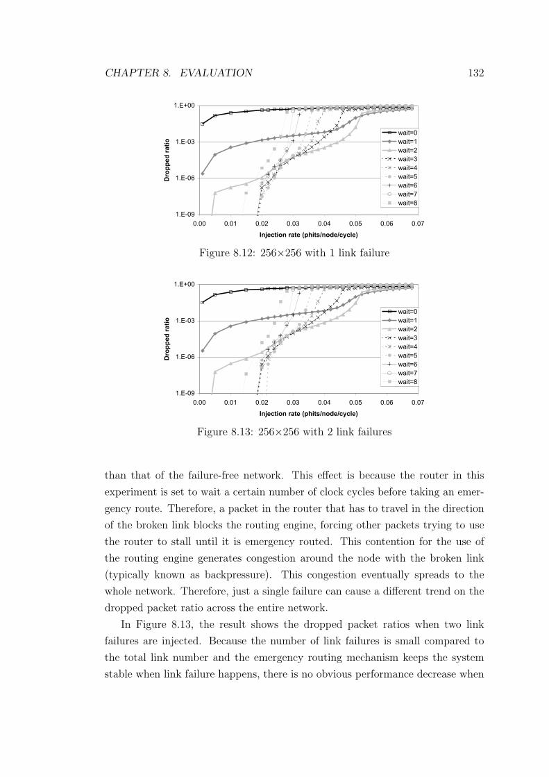
CHAPTER 8. EVALUATION 132
1.E-09
1.E-06
1.E-03
1.E+00
0.00 0.01 0.02 0.03 0.04 0.05 0.06 0.07
Injection rate (phits/node/cycle)
Dropped ratio
wait=0
wait=1
wait=2
wait=3
wait=4
wait=5
wait=6
wait=7
wait=8
Figure 8.12: 256×256 with 1 link failure
1.E-09
1.E-06
1.E-03
1.E+00
0.00 0.01 0.02 0.03 0.04 0.05 0.06 0.07
Injection rate (phits/node/cycle)
Dropped ratio
wait=0
wait=1
wait=2
wait=3
wait=4
wait=5
wait=6
wait=7
wait=8
Figure 8.13: 256×256 with 2 link failures
than that of the failure-free network. This effect is because the router in this
experiment is set to wait a certain number of clock cycles before taking an emer-
gency route. Therefore, a packet in the router that has to travel in the direction
of the broken link blocks the routing engine, forcing other packets trying to use
the router to stall until it is emergency routed. This contention for the use of
the routing engine generates congestion around the node with the broken link
(typically known as backpressure). This congestion eventually spreads to the
whole network. Therefore, just a single failure can cause a different trend on the
dropped packet ratio across the entire network.
In Figure 8.13, the result shows the dropped packet ratios when two link
failures are injected. Because the number of link failures is small compared to
the total link number and the emergency routing mechanism keeps the system
stable when link failure happens, there is no obvious performance decrease when
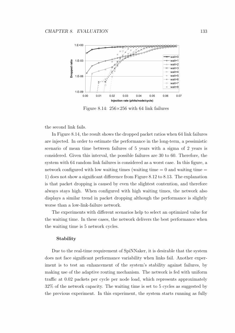
CHAPTER 8. EVALUATION 133
1.E-09
1.E-06
1.E-03
1.E+00
0.00 0.01 0.02 0.03 0.04 0.05 0.06 0.07
Injection rate (phits/node/cycle)
Dropped ratio
wait=0
wait=1
wait=2
wait=3
wait=4
wait=5
wait=6
wait=7
wait=8
Figure 8.14: 256×256 with 64 link failures
the second link fails.
In Figure 8.14, the result shows the dropped packet ratios when 64 link failures
are injected. In order to estimate the performance in the long-term, a pessimistic
scenario of mean time between failures of 5 years with a sigma of 2 years is
considered. Given this interval, the possible failures are 30 to 60. Therefore, the
system with 64 random link failures is considered as a worst case. In this figure, a
network configured with low waiting times (waiting time = 0 and waiting time =
1) does not show a significant difference from Figure 8.12 to 8.13. The explanation
is that packet dropping is caused by even the slightest contention, and therefore
always stays high. When configured with high waiting times, the network also
displays a similar trend in packet dropping although the performance is slightly
worse than a low-link-failure network.
The experiments with different scenarios help to select an optimized value for
the waiting time. In these cases, the network delivers the best performance when
the waiting time is 5 network cycles.
Stability
Due to the real-time requirement of SpiNNaker, it is desirable that the system
does not face significant performance variability when links fail. Another exper-
iment is to test an enhancement of the system’s stability against failures, by
making use of the adaptive routing mechanism. The network is fed with uniform
traffic at 0.02 packets per cycle per node load, which represents approximately
32% of the network capacity. The waiting time is set to 5 cycles as suggested by
the previous experiment. In this experiment, the system starts running as fully
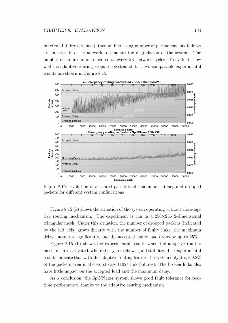
CHAPTER 8. EVALUATION 134
functional (0 broken links), then an increasing number of permanent link failures
are injected into the network to emulate the degradation of the system. The
number of failures is incremented at every 5K network cycles. To evaluate how
well the adaptive routing keeps the system stable, two comparable experimental
results are shown in Figure 8.15.
!"#$%&'(&)*+#',-./)(#0&!*./1!.&0#2#34/55!6&'#789:789
!
"!!
#!!
$!!
%!!
&!!
'!!
(!!
! &!!! "!!!! "&!!! #!!!! #&!!! $!!!! $&!!! %!!!! %&!!! &!!!! &&!!! '!!!!
3/%-;!./,)#*;,*6
#<!*6&.=
>+*;&=
!)!!!
!)!!&
!)!"!
!)!"&
!)!#!
!)!#&
4!*6&.=?*+*;&?),0&
*++,-.,/0123/
435678709,:3;
*<,=3>,09,:3;
9=2--,/0-3+?,.@
" # % A "' $# '% "#A #&' &"# "!#%
!"#$%&'(&)*+#',-./)(#0*./10.&2#3#45/6607&'#89:;89:
!
"!
#!!
#"!
$!!
$"!
%!!
%"!
&!!
&"!
"!!
! "!!! #!!!! #"!!! $!!!! $"!!! %!!!! %"!!! &!!!! &"!!! "!!!! ""!!! '!!!!
4/%-<0./,)#*<,*7
#=0*7&.>
?+*<&>
!(!!!
!(!!"
!(!#!
!(!#"
!(!$!
!(!$"
50*7&.>@*+*<&@),2&
)**+,-+./012.
3245676/8+92:
);+<2=+/8+92:
8<1,,+./,2*>+-?
# $ & @ #' %$ '& #$@ $"' "#$ #!$&
Figure 8.15: Evolution of accepted packet load, maximum latency and droppedpackets for different system confiurations
Figure 8.15 (a) shows the situation of the system operating without the adap-
tive routing mechanism. The experiment is run in a 256×256 2-dimensional
triangular mesh. Under this situation, the number of dropped packets (indicated
by the left axis) grows linearly with the number of faulty links, the maximum
delay fluctuates significantly, and the accepted traffic load drops by up to 25%.
Figure 8.15 (b) shows the experimental results when the adaptive routing
mechanism is activated, where the system shows good stability. The experimental
results indicate that with the adaptive routing feature the system only drops 0.2%
of the packets even in the worst case (1024 link failures). The broken links also
have little impact on the accepted load and the maximum delay.
As a conclusion, the SpiNNaker system shows good fault tolerance for real-
time performance, thanks to the adaptive routing mechanism.

CHAPTER 8. EVALUATION 135
8.6 Layout
The back end design of the router includes floorplanning, initial placement, clock
tree insertion, and final placement and routing. These steps were carried out
using the Synopsis IC Compiler. Then the design was analyzed and verified using
Design Rule Checks (DRC), Layout Versus Schematic (LVS), parasitic extraction,
post-layout timing verification and post layout power analysis.
Figure 8.16 shows a plot of the router layout for the SpiNNaker test chip. The
layout area of the router depends principally on the size of the look-up tables.
The sub-blocks are not shown in the plot because all cells are un-grouped. With
256 multicast routing entries and 2048 point-to-point routing entries – the num-
bers used for the first chip – an area of roughly 1.18mm × 1.42mm = 1.66mm2
is occupied. As can be seen from Figure 8.16, the layout is integrated with the
‘asynchronous↔ synchronous’ interfaces generated by Silistix CHAIN Compiler,
which are pre-synthesized and built as hard macros. These include a ‘Commu-
nications NoC → router’ interface, six ‘router → external link’ interfaces, two
‘router → local processing node’ interfaces, a ‘router AHB slave ↔ System NoC’
interface, and a ‘router AHB master ↔ System NoC’ interface. Because the top
two metal layers (metal 7 and metal 8) are left for top-level routing, the router’s
layout uses only six metal layers (metal 1 – metal 6).
Post-layout timing analysis shows that the clock frequency of the core router
can reach 200 MHz. However, because the ‘asynchronous ↔ synchronous’ inter-
faces have a lower maximum clock frequency for the sake of area efficiency, the
router’s clock is adjusted to the same rate – 166 MHz.
Based on the layout and parasitics extraction, the router’s power performance
is analysed in PrimeTime PX and the power report generated as below:
Global operating voltage: 1.2V
Cell internal power: 14.1mW (80%)
Net switching power: 3.8mW (20%)
Dynamic power (Cell internal power + Net switching power): 17.9mW
(100%)
Cell leakage power: 7.5µW .
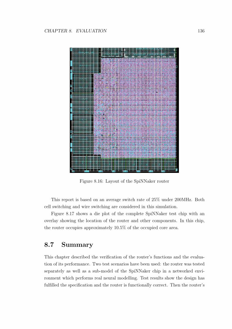
CHAPTER 8. EVALUATION 136
Figure 8.16: Layout of the SpiNNaker router
This report is based on an average switch rate of 25% under 200MHz. Both
cell switching and wire switching are considered in this simulation.
Figure 8.17 shows a die plot of the complete SpiNNaker test chip with an
overlay showing the location of the router and other components. In this chip,
the router occupies approximately 10.5% of the occupied core area.
8.7 Summary
This chapter described the verification of the router’s functions and the evalua-
tion of its performance. Two test scenarios have been used: the router was tested
separately as well as a sub-model of the SpiNNaker chip in a networked envi-
ronment which performs real neural modelling. Test results show the design has
fulfilled the specification and the router is functionally correct. Then the router’s
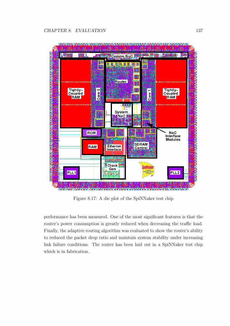
CHAPTER 8. EVALUATION 137
Figure 8.17: A die plot of the SpiNNaker test chip
performance has been measured. One of the most significant features is that the
router’s power consumption is greatly reduced when decreasing the traffic load.
Finally, the adaptive routing algorithm was evaluated to show the router’s ability
to reduced the packet drop ratio and maintain system stability under increasing
link failure conditions. The router has been laid out in a SpiNNaker test chip
which is in fabrication.
Chapter 9
Conclusion
Massive multiprocessor simulators are just becoming feasible with current levels of
technology. Neural simulation is an application which, it is clear, can be mapped
onto such a VLSI system – provided that the interconnection problem can be
solved. The work described in this dissertation demonstrates that a multicast
router can support the traffic expected in a (biological) real-time environment at
a reasonable cost in chip area and without excessive power consumption. The
‘imprecise’, fault-tolerant nature of a neural network can also be exploited by
employing cheap error handling mechanisms to keep the system operating in the
presence of faults, both transient and permanent. It is hoped that this router
makes another small contribution to the ultimate goal of understanding that
most intriguing creation of nature, the human brain.
This dissertation presents a novel communications router, around which, a
universal spiking neural network architecture, SpiNNaker, has been developed.
This yields a GALS-based, scalable multi-chip MPSoC system for the real-time
simulation of large-scale bio-inspired neural networks. The design of this plat-
form emphasizes modelling flexibility, power-efficiency, fault-tolerance and com-
munications throughput; to support these system requirements, various routing
algorithms are implemented in the router. A spiking neural event is defined by
a small packet which holds the address of the firing neuron, for this the router
uses a source address multicast routing mechanism for neural packet switching.
A masked associative memory is implemented to reduce the routing look-up ta-
ble to a practical size. Asynchronous network interfacing and pipeline elasticity
are supported by the router to facilitate GALS-style communication, making the
system scalable.
138
CHAPTER 9. CONCLUSION 139
The router has been designed and implemented as Verilog code and has been
functionally verified by simulation and laid out in UMC 130-nm CMOS technol-
ogy. Post-layout analysis suggests that it is capable of at least its target clock
rate of 200 MHz – faster than the processor cores on this process. Under such a
clock rate, the router derives a throughput of 200M spikes/s. This is enough to
fulfill the system’s target throughput which is an average of 10% of the maximum
throughput. Here the GALS architecture of the chip is important because, in a
large system, the majority of the traffic will simply be routed through to the next
chip and never needs to be synchronized to a local processor. Power analysis
was performed at the gate level, showing that the router with a full traffic load
consumes about 60 mW when running at 200 MHz. The simulation results shows
that the router’s performance can fulfill the system requirements.
A cut-down version of the full router – one with reduced size routing table
but all other features included – has been included on a first, test device; at the
time of writing, this is in fabrication.
9.1 Contributions and limitations
MPSoC is an emerging interest in the field of massively-parallel computing, where
on-chip and/or off-chip routing is a central research focus. Typical high perfor-
mance parallel computing systems consist of high-end processors and low speed
off-chip routers. A significant difference of MPSoCs is that they require lower-
speed and power-efficient processors but high-speed networks. Applying this
cutting-edge technology to neurocomputing has both potential benefits and diffi-
culties. These have been addressed in this dissertation through the router design
for the SpiNNaker system.
9.1.1 Efficient multicast neural event routing
Large-scale neural computing requires intensive communication resources. A ma-
jor contribution of the SpiNNaker router is the design and implementation of the
novel source-address based multicast routing algorithm for neural event communi-
cation. The multicast routing algorithm significantly reduces the overall number
of packets in the network and lightens the traffic load on each individual router.
This is one of the key issues for the SpiNNaker system to achieve its main purpose
– to perform spiking neural simulation efficiently.
CHAPTER 9. CONCLUSION 140
9.1.2 Area
The multicast routing table is distributed across the SpiNNaker nodes, stored
in the associative memories. To achieve a suitable size for on-chip integration,
each routing table is compressed into 1024 words. Compression is achieved by
implementing a masked associative routing algorithm, which routes neural packets
in groups. Further compression is achieved by using default routing that sends an
unrecognized packet to the opposite port to the incoming port, thereby requiring
no routing entry.
The associative memory is implemented using transparent latches, which fur-
ther reduces the die size. Post-layout analysis shows that the area occupation of
the storage units has been reduced by 54% compared to a typical implementation
using D-flip-flops.
9.1.3 Programmability
Since neurocomputing is associated with the structure of neural networks, mod-
elling a neural network requires a procedure for programming the interconnects.
The simulator can be programmed allowing flexibility/experimentation in appli-
cation. The SpiNNaker router has dedicated routing tables to store the inter-
connect information, these are programmable, thus making the router flexible for
modelling different neural networks.
The routing tables can be modified during the computation. Hence a network
can be reconstructed for a follow-up computation, according to the feedback
from the history of the outputs. This allows for an important feature of neural
computing – learning from prior knowledge.
Furthermore, the router can be adjusted according to the current network
situation. For example, under a certain packet injection rate, the router’s waiting
time for adaptive routing has an impact on the average and the maximum packet
latency and the dropped packet ratio. The waiting time can be adjusted to achieve
a reasonable latency and dropped packet ratio. Another example that shows the
importance of knowing the network situation is found in the livelock avoidance
mechanism. When a packet lingers in the network for a period exceeding a
timing threshold, which is usually determined by the maximum packet latency,
the packet is dropped as a livelocked packet. The router is required to be run-time
configurable so that it knows the network’s current time phase.
CHAPTER 9. CONCLUSION 141
9.1.4 Fault-tolerance
The nervous system exhibits a strong ability to tolerate faults. A conventional
digital VLSI system is likely to crash when facing a single fault, whilst a neural
system usually displays graceful degradation. SpiNNaker is a digital VLSI system
emulating the behaviour of biological neural networks and understanding bio-fault
tolerance is one of the primary goals for exploration. Like a neural system that
allows for the loss of spikes, the SpiNNaker router allows for dropping packets
to maintain a certain level of QoS. The reason for introducing a packet dropping
mechanism is that the router performs adaptive routing when congestion persists
for a period of time and a packet will be dropped if adaptive routing causes a
deadlock when it fails. The adaptive routing and the packet dropping mechanism
have been proved to be able to maintain the system stable as well as maintain an
acceptable dropped packet ratio when facing link failures.
The router can also expel an erroneous packet before it tries to route it. This
is done by an error detection mechanism at the first functional stage of the router.
9.1.5 Debugging
Debugging is achieved at system-level. This is realized by the ‘direct’ nearest-
neighbour routing, through which the router can be driven from neighbouring
chips to act as a System NoC master. Through the router’s access to the System
NoC, a faulty chip can be probed, and the chip’s devices can be configured from
outside.
9.1.6 Power efficiency
The SpiNNaker router is designed with some energy-saving features, which help
minimize both the chip- and system-level power consumption. This is achievable
because the actual system is expected to be lightly loaded (approximately 10%
of the maximum supported traffic load) in most cases. The router’s pipeline is
implemented with a traffic-aware mechanism, where a pipeline stage is only acti-
vated when a valid packet has arrived. Because this eliminates any unnecessary
circuit switching caused by ‘empty’ packets, the router maintains its dynamic
power at a minimum while maintaining the capability to deal with packet bursts.
Experiments shows that through this mechanism the dynamic power consump-
tion depends on the packet load as expected. Under 10% of the maximum traffic
CHAPTER 9. CONCLUSION 142
load, the total power saved is by 50% of that under a full traffic load.
9.1.7 Latency insensitivity
Being a GALS system, SpiNNaker is based on a self-timed communication net-
work. Although the router is synchronously implemented, its pipeline is designed
to be latency insensitive under the control of a handshake protocol. There are
three reasons for designing a latency insensitive pipeline. Firstly, it can pause the
traffic inside the router when congestion happens in the router’s asynchronous
output channels. This helps realize the flow control mechanism in the SpiNNaker
system. Secondly, because the off-chip interconnects are slower than the router
pipeline, the router’s pipeline is usually lightly loaded, allowing the router elasti-
cally to buffer the following packets even when the traffic is paused. Finally, the
router allows data injection from different sources that could be either the Com-
munication NoC or the System NoC. When two data flows need to be arbitrated,
the latency insensitive pipeline can stop and stall one of the flows to allow the
other to proceed.
9.1.8 Scalability
The router is responsible for both on- and off-chip communication in the SpiN-
Naker system. Data transactions between routers are conducted via asynchronous
channels. The programmable routers and the asynchronous channels allow for a
flexible construction of a multi-chip network. Therefore, the SpiNNaker system
can be tailored to different scales and network topologies.
9.1.9 Switching techniques
The SpiNNaker router uses store-and-forward routing because a neural packet is
relatively small (typically 40 bits) and independent of others. Unlike a worm-
hole router or a virtual channel router which handles flow-control at the flit
level, thereby minimizing buffer requirements, a store-and-forward router requires
buffering of the complete packet before forwarding it; this usually results in a large
buffer space for one or more packets. However, flit-level switching is unsuitable
for neural packet routing because a routing decision has to be made on the ba-
sis of the complete neural packet. As the packets are small in SpiNNaker, the

CHAPTER 9. CONCLUSION 143
store-and-forward scheme is acceptable in terms of buffer area and furthermore,
it avoids flit-dependent deadlock.
9.1.10 Pipelining
The SpiNNaker router is deeply pipelined, reducing cycle time, which allows the
router to process a large number of spiking neurons in parallel. Pipelining doesn’t
reduce router latency, rather it increases it due to additional latencies through
pipeline registers. This may have an impact on the boot-up and management
time of the system, which relies on the point-to-point and nearest-neighbour
routing. However, electronic communication latency in is not an important issue
for neurocomputing. The 200 MHz router is capable of routing 200K spiking
neurons (all at a firing rate of 1000 Hz) within the biological time unit (1ms).
9.1.11 Monitoring
Counters have been included to allow the network traffic to be monitored. They
can be used to obtain valuable experiment results, such as the real traffic pattern
of a neural network. In addition, monitoring the traffic is useful for system
debugging and verification.
9.2 Future work
The router presented in this thesis has left many open issues to be investigated.
Indeed, since the proposed SpiNNaker system is designed for experimental pur-
poses in the field of biologically-inspired spiking neural modelling, it is expected
that much future work will be carried out based on this system. Therefore, one of
the major aims in designing the SpiNNaker router is to provide enough flexibility
to adapt various kinds of application to the system and to obtain the required
performance. Some of the experimental research is already ongoing or will be
carried out in the near future. The work discussed below may provide a better
performance and more concrete results.
CHAPTER 9. CONCLUSION 144
9.2.1 Alternative implementation of the CAM
Area optimization is an important issue for on-chip router design. The CAM
occupies a large proportion of the router’s area, this could be reduced using an
alternative implementation utilising custom design. A typical custom-built VLSI
ternary CAM cell uses SRAM cells for bit storage which is implemented using 16
transistors [PS06]. Although a custom-built CAM would be expensive to design
and reduces process portability, it might be worthwhile replacing the current
CAM given enough time for the development.
9.2.2 QoS enhancements
Neural communication is special in terms of its traffic pattern. This leads to the
challenge of supporting application demand QoS on the SpiNNaker system. One
principal approach to QoS is to parameterize the system. The SpiNNaker router
is highly configurable, providing many possibilities to enhance QoS after the
platform has been constructed. Some QoS issues on the SpiNNaker are discussed
below, including end-to-end delay and packet recovery.
Multicast routing is more likely to create traffic hot spots than unicast routing
because it duplicates packets. These hot spots may cause transient link conges-
tion, resulting occasionally in bad end-to-end delays. The traffic in a certain
neural application usually obeys a certain pattern, which can be observed by the
router’s 8 packet counters. By analysing statistical results, a QoS scheme can
be developed to minimize the end-to-end delays. This can be applied onto the
network by reprogramming the routing tables.
A link/node failure is another possible cause for long end-to-end delays and
there are at least two potential situations resulting in this in the SpiNNaker
system. A well-defined multicast routing strategy usually uses multicast trees for
packet delivery. A multicast packet traverses a tree and is duplicated when it
reaches a branch point of the tree. Under this circumstance, any blockage at the
intermediate link or node of the tree will disrupt the service because adaptive
routing will be invoked, increase routing latency. A similar situation happens in
the default routing which is expected to be used extensively in the SpiNNaker
system. In chapter 8, the experiment of tuning a 256×256 SpiNNaker network
model showed that the router’s waiting time has a great impact on the network
latency. By adjusting the waiting time and the adaptive routing mechanism,

CHAPTER 9. CONCLUSION 145
the system can achieve a better QoS where the dropped packet ratio, network
latency and system stability are well balanced. These factors are considered when
adjusting the router: failure rate, network scale (failure numbers) and the time
the failure exists for.
Multicast routing QoS is influenced by the construction of the multicast tree.
There are two main approaches for multicast tree construction: the Steiner min-
imal tree protocol and the centre-based protocol. The two protocols provide
different aspects of QoS. For example, in the Steiner minimal tree protocol, each
branch of the tree is usually the shortest path from the sender to the receiver,
hence it guarantees the shortest end-to-end delay [SM02]. To achieve certain
QoS, multicast trees are rearranged through reprogramming the routing tables.
The router is implemented with two fault recovery mechanisms controlled
by software. The first is dropped packet recovery. Although neural simulation
usually allows packet loss, it is also the case that some packets must not be lost.
A dropped packet is dumped into a register in the router, and is readable by the
system through the Monitor Processor, thus the system has an opportunity to
decide whether to disregard the packet or reissue it. The second mechanism is
the ability to probe and recover a dead chip. One possible case is the resetting
of a Monitor Processor from a neighbouring chip, this is done using the nearest
neighbour routing.
In addition to dropped packet recovery, another way to guarantee packet
arrival is setting the waiting time value of the router. For example, in the PDP
model, spike loss is not tolerated, while delay can be tolerated. Therefore, the
waiting time before dropping a packet can be an infinite value.
9.2.3 Intermediate circuit test chip
The intermediate circuit test chip is in fabrication while this dissertation is being
written. This will be used for preliminary system-level verification, based upon
which the final SpiNNaker chip will be implemented. In order to fulfill the min-
imum requirements, it contains a basic subset of the communication framework,
including the router, the Communications NoC, the System NoC and the net-
work interfaces. It also contains the essential on-chip devices, such as the ARM
processing cores, the off-chip memory controller, the on-chip memories, etc.
The verification process of the test chip will be similar as the RTL level veri-
fication mentioned in chapter 8. The hardware platform can run more extensive
CHAPTER 9. CONCLUSION 146
real applications in a reasonable time. A test can be performed on a single chip
with its external ports wrapped around, or on multiple chips, interconnected with
each other on a PCB test board. For the verification of the router, firstly routing
tables are initialized during chip start-up. This is a process of testing the router’s
initialization behaviour controlled by the Monitor Processor through the System
NoC. After initialization, a neural network is mapped onto the system. The fas-
cicle processor(s) then start generating neural spikes which are transmitted by
the router to appropriate destinations. This is a process for testing the routing
functions. Other functions, such as debugging, packet counting, error handling,
can also be tested.
Because of the chip’s experimental purpose, its router is highly configurable.
A slight reduction in the router’s area could also be achieved by removing or
simplifying some of the router’s components in a future chip. For example, the
router has a programmable timer to set the waiting time before invoking the
adaptive routing. The time can be adjusted to achieve a reasonable packet drop
rate and system stability. However, it is possible that an optimal value of the
waiting time is obtained based on extensive chip simulations. The timer then no
longer needs to be programmed and can be simplified.
9.3 Perspective of neurocomputing on NoCs
Neurocomputing is regarded as an important scientific objective in future com-
putational architectures. The exploration of neural modelling has been carried
out on the basis of conventional technologies, which although progress has been
made, still have difficulties addressing two significant features of real biological
systems – real-time interactions and large-scale computation. NoCs have also
been regarded as an important technology for future parallel computers, while
most research in this area has been aimed at more conventional applications such
as multimedia processing. This thesis aimed to combine the benefit of both the
research areas and explore a novel router architecture.
It is hoped that, based upon the work described in this thesis, a NoC-based
MPSoC will show clear advantage for modelling large-scale spiking neural net-
works for the exploration of learning and other purposes. It is also hoped that in
the near future, research in the area of parallel computing can also benefit from
the exploration of neurocomputing.
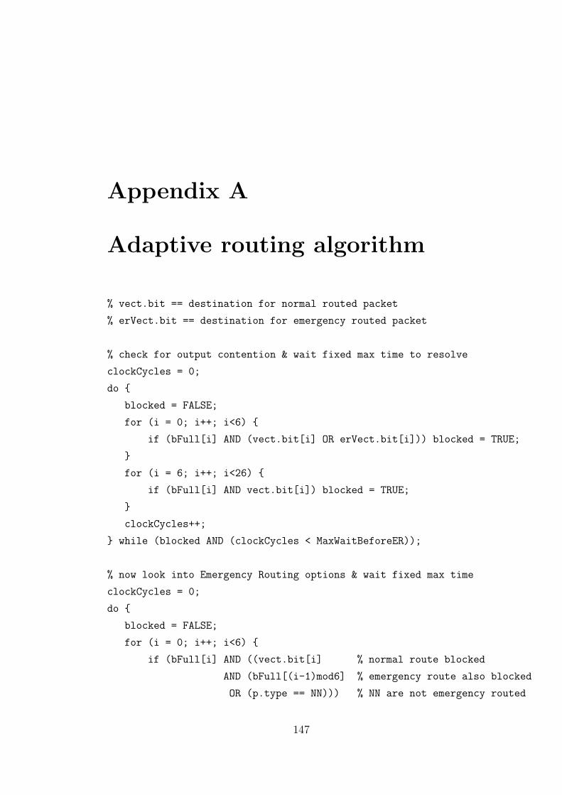
Appendix A
Adaptive routing algorithm
% vect.bit == destination for normal routed packet
% erVect.bit == destination for emergency routed packet
% check for output contention & wait fixed max time to resolve
clockCycles = 0;
do {
blocked = FALSE;
for (i = 0; i++; i<6) {
if (bFull[i] AND (vect.bit[i] OR erVect.bit[i])) blocked = TRUE;
}
for (i = 6; i++; i<26) {
if (bFull[i] AND vect.bit[i]) blocked = TRUE;
}
clockCycles++;
} while (blocked AND (clockCycles < MaxWaitBeforeER));
% now look into Emergency Routing options & wait fixed max time
clockCycles = 0;
do {
blocked = FALSE;
for (i = 0; i++; i<6) {
if (bFull[i] AND ((vect.bit[i] % normal route blocked
AND (bFull[(i-1)mod6] % emergency route also blocked
OR (p.type == NN))) % NN are not emergency routed
147
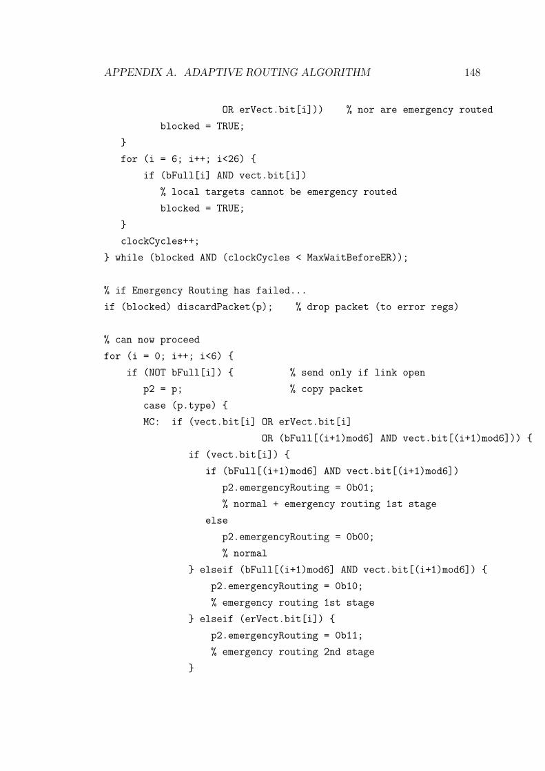
APPENDIX A. ADAPTIVE ROUTING ALGORITHM 148
OR erVect.bit[i])) % nor are emergency routed
blocked = TRUE;
}
for (i = 6; i++; i<26) {
if (bFull[i] AND vect.bit[i])
% local targets cannot be emergency routed
blocked = TRUE;
}
clockCycles++;
} while (blocked AND (clockCycles < MaxWaitBeforeER));
% if Emergency Routing has failed...
if (blocked) discardPacket(p); % drop packet (to error regs)
% can now proceed
for (i = 0; i++; i<6) {
if (NOT bFull[i]) { % send only if link open
p2 = p; % copy packet
case (p.type) {
MC: if (vect.bit[i] OR erVect.bit[i]
OR (bFull[(i+1)mod6] AND vect.bit[(i+1)mod6])) {
if (vect.bit[i]) {
if (bFull[(i+1)mod6] AND vect.bit[(i+1)mod6])
p2.emergencyRouting = 0b01;
% normal + emergency routing 1st stage
else
p2.emergencyRouting = 0b00;
% normal
} elseif (bFull[(i+1)mod6] AND vect.bit[(i+1)mod6]) {
p2.emergencyRouting = 0b10;
% emergency routing 1st stage
} elseif (erVect.bit[i]) {
p2.emergencyRouting = 0b11;
% emergency routing 2nd stage
}

APPENDIX A. ADAPTIVE ROUTING ALGORITHM 149
ParityFix(p2.parity);
sendPacketTo(p2, buff[i]);
}
P2P: if (vect.bit[i] OR (bFull[(i+1)mod6] AND vect.bit[(i+1)mod6]))
sendPacketTo(p2, buff[i]);
NN: if (vect.bit[i])
sendPacketTo(p2, buff[i]);
} % end case
} % end if
} % end for
for (i = 6; i++; i<26) {
if (vect.bit[i]) {
p2 = p;
if (p2.type == NN) p2.route = src;
sendPacketTo(p2, buff[i]);
}
}

Appendix B
Registers definitions
B.1 Register summary
A summary of the configuration registers is given in Table B.1.
Name Offset R/W Function
r0: control 0×0 R/W router control registerr1: status 0×4 R router statusr2: error header 0×8 R error packet control byte and flagsr3: error routing 0×C R error packet routing wordr4: error payload 0×10 R error packet data payloadr5: error status 0×14 R error packet statusr6: dump header 0×18 R dumped packet control byte and flagsr7: dump routing 0×1C R dumped packet routing wordr8: dump payload 0×20 R dumped packet data payloadr9: dump outputs 0×24 R dumped packet intended destinationsr10: dump status 0×28 R dumped packet statusrT1: test register 0×F00 R/W hardware test register 1rT2: test key 0×F04 R/W hardware test register 2
- CAM input test key
Table B.1: Register summary
The detailed register definitions are listed at the following:
B.2 Register 0 (r0): control
The functions of r0 are described in Table B.2.
150

APPENDIX B. REGISTERS DEFINITIONS 151
31 30 29 28 27 26 25 24 23 22 21 20 19 16 15 14 13 12 11 10 9 8 7 6 5 4 3 2 1 0
RDMP[4:0]
18 17
wait2[3:0] wait1[3:0] ETPW
Figure B.1: Register 0 definition
Name bits R/W Function
R 0 R/W enable packet routingE 1 R/W enable error packet interruptD 2 R/W enable dump packet interruptTP 7:6 R/W time phase (c.f. packet time stamps)MP[4:0] 12:8 R/W Monitor Processor ID numberW 15 W re-initialise wait counterswait1[7:0] 23:16 R/W wait time before emergency routingwait2[7:0] 31:24 R/W wait time before dropping packet
Table B.2: Register 0 – router control register
B.3 Register 1 (r1): status
29 28 27 26 25 24 23 22 21 20 19 16 15 14 13 12 11 10 9 8 7 6 5 4 3 2 1 018 1731 30
E ctr[7:0]D ER BI
Figure B.2: Register 1 definition
All router interrupt request sources are visible r1, as is the current status of
the emergency routing system.
The functions of r1 are described in Table B.3.
The router generates three interrupt request outputs that are handled by the
vectored interrupt controller (VIC) on each processor: diagnostic counter event
interrupt, dump interrupt and error interrupt. These correspond to the OR of
ctr[7:0], D and E respectively.
The interrupt requests are cleared by reading their respective individual status
registers: Register 5, Register 10 and Register 2N.

APPENDIX B. REGISTERS DEFINITIONS 152
Name bits R/W Function
ctr[7:0] 7:0 R diagnostic counter interrupt activeB 16 R busy - active packet(s) in router pipelineER[1:0] 25:24 R emergency routing status (clear, wait1, wait2)D: dump int 29 R dump packet interrupt activeE: error int 30 R error packet interrupt activeI: interrupt active 31 R combined router interrupt request
Table B.3: Register 1 – router status
B.4 Register 2 (r2): error header
A packet which contains an error is copied to Registers 2 to 5. Once a packet
has been copied (indicated by bit[31] of Register 5 being set) any further error
packet is ignored, except that it can update the sticky bits in Register 5 (and can
be counted by a suitably-configured diagnostic counter).
29 28 27 26 25 24 23 22 21 20 19 16 15 14 13 12 11 10 9 8 7 6 5 4 3 2 1 018 1731 30
P F T Route TPcontrol byte
Figure B.3: Register 2 definition
The functions of r2 are described in Table B.4.
Name bits R/W Function
TP: time phase 7:6 R time phase when packet receivedControl byte 23:16 R control byte of error packetRoute 26:24 R Rx route field of error packetT: TP error 27 R packet time stamp errorF: framing error 28 R packet framing errorP: parity 29 R packet parity error
Table B.4: Register 2 – error header
B.5 Register 3 (r3): error routing

APPENDIX B. REGISTERS DEFINITIONS 153
29 28 27 26 25 24 23 22 21 20 19 16 15 14 13 12 11 10 9 8 7 6 5 4 3 2 1 018 1731 30
32−bit routing word
Figure B.4: Register 3 definition
B.6 Register 4 (r4): error payload
29 28 27 26 25 24 23 22 21 20 19 16 15 14 13 12 11 10 9 8 7 6 5 4 3 2 1 018 1731 30
32−bit data payload
Figure B.5: Register 4 definition
B.7 Register 5 (r5): error status
29 28 27 26 25 24 23 22 21 20 19 16 15 14 13 12 11 10 9 8 7 6 5 4 3 2 1 018 1731 30
V F TP TS error countUE
Figure B.6: Register 5 definition
Name bits R/W Function
TS error count 15:0 R time stamp error countU: undefined 26 R undefined packet type [=11] (sticky)T: TP error 27 R packet time stamp error (sticky)F: framing error 28 R packet framing error (sticky)P: parity 29 R packet parity error (sticky)V: overflow 30 R more than one error packet detectedE: error 31 R error packet detected
Table B.5: Register 5 – error status
The Monitor Processor resets Register 5 by reading its contents. The functions
of r5 are described in Table B.5.

APPENDIX B. REGISTERS DEFINITIONS 154
B.8 Register 6 (r6): dump header
A packet which is dumped because it cannot be routed to its destinations is copied
to Registers 6 to 10. Once a packet has been dumped (indicated by bit[31] of
Register 10 being set) any further packet that is dumped is ignored, except that
it can update the sticky bits in Register 10 (and can be counted by a suitably-
configured diagnostic counter).
29 28 27 26 25 24 23 22 21 20 19 16 15 14 13 12 11 10 9 8 7 6 5 4 3 2 1 018 1731 30
Route TPcontrol byte
Figure B.7: Register 6 definition
Name bits R/W Function
TP: time phase 7:6 R time phase when packet dumpedControl byte 23:16 R control byte of dumped packetRoute 26:24 R Rx route field of dumped packet
Table B.6: Register 6 – dump header
The functions of r6 are described in Table B.6.
B.9 Register 7 (r7): dump routing
29 28 27 26 25 24 23 22 21 20 19 16 15 14 13 12 11 10 9 8 7 6 5 4 3 2 1 018 1731 30
32−bit routing word
Figure B.8: Register 7 definition
B.10 Register 8 (r8): dump payload

APPENDIX B. REGISTERS DEFINITIONS 155
29 28 27 26 25 24 23 22 21 20 19 16 15 14 13 12 11 10 9 8 7 6 5 4 3 2 1 018 1731 30
32−bit data payload
Figure B.9: Register 8 definition
29 28 27 26 25 24 23 22 21 20 19 16 15 14 13 12 11 10 9 8 7 6 5 4 3 2 1 018 1731 30
FPE[19:0] LE[5:0]
Figure B.10: Register 9 definition
Name bits R/W Function
LE[5:0] 5:0 R Tx link transmit error caused packet dumpFPE[19:0] 25:6 R Fascicle Processor link error caused dump
Table B.7: Register 9 – dump outputs
B.11 Register 9 (r9): dump outputs
The functions of r9 are described in Table B.7.
B.12 Register 10 (r10): dump status
29 28 27 26 25 24 23 22 21 20 19 16 15 14 13 12 11 10 9 8 7 6 5 4 3 2 1 018 1731 30
FPE[19:0] LE[5:0]VD
Figure B.11: Register 10 definition
The Monitor Processor resets Register 10 by reading its contents. The func-
tions of r10 are described in Table B.8.
Name bits R/W Function
LE[5:0] 5:0 R Tx link error caused dump (sticky)FPE[19:0] 25:6 R Fascicle Proc link error caused dump (sticky)V: overflow 30 R more than one packet dumpedD: dumped 31 R packet dumped
Table B.8: Register 10 – dump status

APPENDIX B. REGISTERS DEFINITIONS 156
B.13 Register T1 (rT1): hardware test register
29 28 27 26 25 24 23 22 21 20 19 16 15 14 13 12 11 10 9 8 7 6 5 4 3 2 1 018 1731 30
V entry M
Figure B.12: Register T1 definition
This register is used for hardware test purposes. The functions of rT1 are
described in Table B.9.
Name bits R/W Function
M 0 R MC router associative look-up ‘miss’ outputentry 10:1 R MC router associative look-up entry addressV 31 R register T1 contents are valid
Table B.9: Register T1 – hardware test register 1
The input key used for the associative look-up whenever this register is read
is in Register T2. When a new value is written into Register T2 bit[31] ‘V’ will
be low until the new value has propagated through the pipeline, whereupon ‘V’
will go high to signify that the test results are available in Register T1.
B.14 Register T2 (rT2): hardware test key
29 28 27 26 25 24 23 22 21 20 19 16 15 14 13 12 11 10 9 8 7 6 5 4 3 2 1 018 1731 30
32−bit key
Figure B.13: Register T2 definition
This register holds the key presented to the association input to the multicast
router when Register T1 is read.

Bibliography
[BB98] J.M. Bower and D. Beeman. The book of GENESIS: Exploring re-
alistic neural models with the general simulation system. Springer,
2nd edition, 1998.
[BCRC05] C. Boucheny, R. Carrillo, E. Ros, and O. Coenen. Real-time spiking
neural network: An adaptive cerebellar model. Lecture Notes in
Computer Science, 3512:136–144, June 2005.
[BF02] J. Bainbridge and S.B. Furber. Chain: A delay-insensitive chip area
interconnect. IEEE Micro, 22(5):16, September-October 2002.
[BJ90] R. Beale and T. Jackson. Neural Computing: an introduction. Taylor
and Francis, Inc., 1990.
[BMJ+98] J. Broch, D. Maltz, D. Johnson, Y. Hu, and J. Jetcheva. A per-
formance comparison of multi-hop wireless ad hoc network routing
protocols. In Proceedings of the 4th Annual ACM/IEEE Interna-
tional Conference on Mobile Computing and Networking, pages 85–
97, 1998.
[Boa00] K. Boahen. Point-to-point connectivity between neuromorphic chips
using address events. IEEE Transactions on Circuits and Systems
II: Analog and Digital Signal Processing, 47:416–434, April 2000.
[Cha84] D. Chapiro. Globally-asynchronous locally-synchronous systems.
Doctoral Thesis, Dept. of Computer Science, Stanford Univ., 1984.
[CN99] S. Chen and K. Nahrstedt. Distributed quality-of-service routing in
ad hoc networks. IEEE Journal on Selected Areas in Communica-
tions, 17(8):1488–1505, August 1999.
157
BIBLIOGRAPHY 158
[Con97] B. Cong. On embeddings of neural networks into massively parallel
computer systems. In Proceedings of IEEE 1997 National Aerospace
and Electronics Conference, 1:231–238, July 1997.
[CSM94] S. Cavalieri, A. Stefano, and O. Mirabella. Distributed routing in
packet-switching networks by counter propagation network. Applied
Intelligence, 4(1):67–82, March 1994.
[CW06] K. Chen and L. Wang. Trends in neural computation (studies in
computational intelligence). Springer, 2006.
[DBG+03] Dall’Osso, M. Biccari, G. Giovannini, L.D. Bertozzi, and L. Benini.
Xpipes: A latency insensitive parameterized network-on-chip archi-
tecture for multiprocessor SoCs. In Proceedings of 21st International
Conference on Computer Design, pages 536– 539, October 2003.
[DC00] W.J. Dally and A. Chang. The role of custom design in ASIC chips.
In Proceedings of the 37th Annual Design Automation Conference,
pages 643–647, 2000.
[DM03] T. Dumitras and R. Marculescu. On-chip stochastic communication.
In Proceedings of the conference on Design, Automation and Test in
Europe - Volume 1, page 10790, 2003.
[DT03] W. Dally and B. Towles. Principles and practices of interconnection
networks. Morgan Kaufmann, 2003.
[DYN03] J. Duato, S. Yalamanchili, and L. M. Ni. Interconnection networks:
an engineering approach. Morgan Kaufmann, 2nd edition, 2003.
[FB09] S.B. Furber and A.D. Brown. Biologically-inspired massively-
parallel architectures - computing beyond a million processors. In
Proceedings of the 9th International Conference on the Application
of Concurrency to System Design (ACSD’09), 0:3–12, July 2009.
[FRS+87] B.M. Forrest, D. Roweth, N. Stroud, D.J. Wallace, and G.V. Wilson.
Implementing neural network models on parallel computers. The
Computer Journal, 30(5):413–419, October 1987.

BIBLIOGRAPHY 159
[FT07] S.B. Furber and S. Temple. Neural systems engineering. Journal of
the Royal Society interface, 4(1):193–206, April 2007.
[FTB06] S.B. Furber, S. Temple, and A.D. Brown. High-performance com-
puting for systems of spiking neurons. In Proceedings of AISB’06
Workshop on GC5: Architecture of Brain and Mind, 2:29–32, April
2006.
[Get89] P.A. Getting. Emerging principles governing the operation of neural
networks. Annual Review of Neuroscience, 12:185–204, March 1989.
[GG00] P. Guerrier and A. Greiner. A generic architecture for on-chip
packet-switched interconnections. In Proceedings of the Conference
on Design, Automation and Test, pages 250–256, 2000.
[GGG+07] C. Gomez, F. Gilabert, M.E. Gomez, P. Lopez, and J. Duato. De-
terministic versus adaptive routing in fat-trees. In Proceedings of
IEEE International Parallel and Distributed Processing Symposium
as a part of IPDPS, pages 1–8, March 2007.
[GK02] W. Gerstner and W. Kistler. Spiking neuron models: single neurons,
populations, plasticity. Cambridge University Press, 2002.
[Gur97] K. Gurney. An Introduction to neural networks. CRC Press, 1997.
[Ham91] D. Hammerstrom. A highly parallel digital architecture for neural
network emulation. In: Delgado-Frias, J. G. and Moore, W. R.
(eds.), VLSI for artificial intelligence and neural networks. Plenum
Press, 1991.
[Hay98] S. Haykin. Neural networks: A comprehensive foundation. Prentice
Hall PTR, 1998.
[HC97] M.L. Hines and N.T. Carnevale. The NEURON simulation environ-
ment. Neural Computation, 9(6):1179–1209, August 1997.
[Hee95] J. Heemskerk. Overview of Neural Hardware: Neurocomputers for
Brain-Style Processing. Design, Implementation and Application,
PhD thesis. Unit of Experimental an Theoretical Psychology, Leiden
University, Netherlands, 1995.

BIBLIOGRAPHY 160
[HM04] J. Hu and R. Marculescu. DyAD: Smart routing for Networks-on-
Chip. In Proceeding of the 41st Design Automation Conference,
pages 260–263, June 2004.
[Izh03] E. Izhikevich. Simple model of spiking neurons. IEEE Transactions
on Neural Networks, 14(6):1569–1572, November 2003.
[Izh04] E. Izhikevich. Which model to use for cortical spiking neurons. IEEE
Transactions on Neural Networks, 15:1063–1070, 2004.
[JFW08] X. Jin, S.B. Furber, and V. Woods. Efficient modelling of spiking
neural networks on a scalable chip multiprocessor. In the Proceedings
of International Joint Conference on Neural Networks, pages 2813–
2820, June 2008.
[JSR+97] A. Jahnke, T. Schoenauer, U. Roth, K. Mohraz, and H. Klar. Sim-
ulation of spiking neural networks on different hardware platforms.
Lecture Notes in Computer Science, 1327:1187–1192, 1997.
[KKS+07] A. Kumar, P. Kundu, A. Singh, L. Peh, and N. Jha. A 4.6Tbit-
s/s 3.6GHz single-cycle NoC router with a novel switch allocator in
65nm CMOS. In Proceedings of International Conference on Com-
puter Design, pages 63–70, October 2007.
[KS85] E.R. Kandel and J.H. Schwartz. Principles of neural science. Else-
vier, 2nd edition, 1985.
[LFJ+10] M. Lujan, S.B. Furber, X. Jin, M. Khan, D. Lester, J. Miguel-
Alonsoy, J. Navaridasy, E. Painkras, L.A. Plana, A. Rast,
D. Richards, Y. Shi, S. Temple, J. Wu, and S. Yang. Fault-tolerance
in the SpiNNaker architecture. IEEE Transactions on Computers
(submitted), 2010.
[LKPD05] M. Lengyel, J. Kwag, O. Paulsen, and P. Dayan. Matching stor-
age and recall: Hippocampal spike timing-dependent plasticity and
phase response curves. Nature Neuroscience, 8(12):1677–1683, De-
cember 2005.
[LYJ06] Z. Lu, B. Yin, and A. Jantsch. Connection-oriented multicasting in
wormhole-switched Networks on Chip. In Proceedings of the IEEE
BIBLIOGRAPHY 161
Computer Society Annual Symposium on Emerging VLSI Technolo-
gies and Architectures, page 205, March 2006.
[Mac97] Advanced RISC Machines. AMBA, advanced microcontroller bus
architecture specification. ARM IHI 0001 D, April 1997.
[Mah92] M. Mahowald. VLSI analogs of neuronal visual processing: A syn-
thesis of form and function, Ph.D. dissertation. California Institu-
tion of Technology., 1992.
[Mar06] H. Markram. The blue brain project. Nature reviews neuroscience,
7:153–160, February 2006.
[Mas56] S.J. Mason. Feedback theory: further properties of signal flow graphs.
Cambridge, Mass., 3rd edition, 1956.
[MB90] N. Morgan and H. Bourlard. Continuous speech recognition using
multilayer perceptrons with hidden markov models. In Proceedings
of IEEE International Conference on Acoustics, Speech, and Signal
Processing, pages 413–416, 1990.
[MC93] Y.K. Muthusamy and R.A. Cole. A segment-based automatic lan-
guage identification system. Advances in Neural Information Pro-
cessing Systems, 4:241, 1993.
[MHK+99] T. Meincke, A. Hemani, S. Kumar, P. Ellervee, J. Oberg, T. Olsson,
P. Nilsson, D. Lindqvist, and H. Tenhunen. Globally asynchronous
locally synchronous architecture for large high-performance ASICs.
In Proceedings of the 1999 IEEE International Symposium on Cir-
cuits and Systems. ISCAS, 1:512–515, 1999.
[MHM96] T.H. Martin, B.D. Howard, and B. Mark. Neural network design.
PWS Publishing Company, 1996.
[Moi06] H.P. Moisy. Spiking neuron networks – A survey. IDIAP Research
Report, (11), 2006.
[MT99] T. Miyoshi and Y. Tanaka. Optimal hierarchical structure of broad-
cast network. Electronics and Communications in Japan, 82(2):48–
56, January 1999.
BIBLIOGRAPHY 162
[NLMA+08] J. Navaridas, M. Lujan, J. Miguel-Alonso, L.A. Plana, and S.B.
Furber. Evaluation of a large-scale SpiNNaker system. Actas de las
XIX Jornadas de Paralelismo. Castellon, pages 662–667, September
2008.
[NLMA+09] J. Navaridas, M. Lujan, J. Miguel-Alonso, L.A. Plana, and S.B.
Furber. Understanding the interconnection network of SpiNNaker.
In Proceedings of the 23rd International Conference on Supercom-
puting, pages 286–295, June 2009.
[Pat07] J.H. Patel. Manufacturing process variations and dependability – A
contrarian view. In Proceedings of IEEE/IFIP DSN-2007 (Supple-
mental Volume), 2007.
[PEM+07] H. Plesser, J. Eppler, A. Morrison, M. Diesmann, and M. Gewaltig.
Efficient parallel simulation of large-scale neuronal networks on clus-
ters of multiprocessor computers. Lecture Notes in Computer Sci-
ence, 4641:672–681, August 2007.
[PFB+08] L.A. Plana, S.B. Furber, J. Bainbridge, S. Salisbury, Y. Shi, and
J. Wu. An on-chip and inter-chip communications network for the
SpiNNaker massively-parallel neural net simulator. In Proceedings of
the 2nd IEEE International Symposium on Network-on-Chip, pages
215–216, April 2008.
[PFT+07] L.A. Plana, S.B. Furber, S. Temple, M. Khan, Y. Shi, J. Wu, and
S. Yang. A GALS infrastructure for a massively parallel multi-
processor. IEEE Design and Test of Computers, 24(5):454–463,
September-October 2007.
[PS06] K. Pagiamtzis and A. Sheikholeslami. Content-addressable mem-
ory (CAM) circuits and architectures: a tutorial and survey. IEEE
Journal of Solid-State Circuits, 41, 2006.
[Ram92] U. Ramacher. SYNAPSE: A neurocomputer that synthesizes neural
algorithms on a parallel systolic engine. Journal of Parallel and
Distributed Computing, 14(3):306–318, 1992.

BIBLIOGRAPHY 163
[RC96] D. Rajeev and B. Craig. Efficient broadcast and multicast on mul-
tistage interconnection networks using multiport encoding. IEEE
Transactions on Parallel and Distributed Systems, page 36, October
1996.
[RCO+06] E. Ros, R. Carrillo, E.M. Ortigosa, B. Barbour, and R. Agis. Event-
driven simulation scheme for spiking neural networks using lookup
tables to characterize neuronal dynamics. Neural Computation,
18(2):2959–2993, December 2006.
[RM86] D. Rumelhart and L. McClelland. Parallel distributed processing:
explorations in the microstructure of cognition, volume 1: Founda-
tions. MIT Press, 1986.
[RMA05] F.J. Ridruejo and J. Miguel-Alonso. INSEE: An interconnection
network simulation and evaluation environment. Lecture Notes in
Computer Science, 3648:1014–1023, 2005.
[RRH+95] U. Ramacher, W. Raab, J.A.U. Hachmann, J. Beichter, N. Bruls,
M. Wesseling, E. Sicheneder, J. Glass, A. Wurz, and R. Manner.
SYNAPSE-1: A high-speed general purpose parallel neurocomputer
system. In Proceedings of 9th International Parallel Processing Sym-
posium, pages 774–781, April 1995.
[RYKF08] A.D. Rast, S. Yang, M.M. Khan, and S.B. Furber. Virtual synaptic
interconnect using an asynchronous Network-on-Chip. In Proceed-
ings of 2008 International Joint Conference on Neural Networks,
pages 2727–2734, June 2008.
[SHG08] F.A. Samman, T. Hollstein, and M. Glesner. Multicast parallel
pipeline router architecture for Network-on-Chip. In Proceedings of
the Conference on Design, Automation and Test in Europe, pages
1396–1401, 2008.
[Sil02] Brains In Silicon. Extended address event representation draft stan-
dard. Stanford University, 2002.
[Siv91] M. Sivilotti. Wiring considerations in analog VLSI systems, with
application to field-programmable networks, Ph.D. dissertation. Cal-
ifornia Institute of Technology., 1991.
BIBLIOGRAPHY 164
[SK93] C. Su and G.S. Kang. Adaptive deadlock-free routing in multi-
computers using only one extra virtual channel. In Proceedings of
International Conference on Parallel Processing, 1:227–231, 1993.
[SM02] A. Striegel and G. Manimaran. A survey of QoS multicasting issues.
IEEE Communications Magazine, 40(6):82–87, June 2002.
[SMJK98] T. Schoenauer, N. Mehrtash, A. Jahnke, and H. Klar. MASPINN:
Novel concepts for a neuro-accelerator for spiking neural networks.
In Proceedings of VIDYNN98, 3728:562–569, June 1998.
[SZX07] Q. Sun, M. Zhang, and L. Xiao. Hardware-based multicast with
global load balance on k-ary n-trees. In Proceedings of the 2007
International Conference on Parallel Processing, page 21, September
2007.
[TDR01] S. Thorpe, A. Delorme, and R. Van Rullen. Spike-based strategies
for rapid processing. Neural Network, 14:715–725, 2001.
[THH01] D. Tutsch, M. Hendler, and G. Hommel. Multicast performance of
multistage interconnection networks with shared buffering. Lecture
Notes in Computer Science, 2093, 2001.
[Tuc88] H.C. Tuckwell. Introduction to theoretical neurobiology. Cambridge
University Press, 1988.
[VG01] F. Vahid and T. Givargis. Platform tuning for embedded systems
design. IEEE Computer, 34(3):112–114, March 2001.
[Vig94] S.S. Viglione. Applications of pattern recognition technology. A
Prelude to Neural Networks: Adaptive and Learning Systems, pages
115–162, 1994.
[Vre02] J. Vreeken. Spiking neural networks: an introduction. Technical Re-
port UU-CS-2003-008, Artificial Intelligence laboratory, Intelligent
Systems Group, Univ. Utrecht, 2002.
[VSVJ89] M. Verleysen, B. Sirletti, A.M. Vandemeulebroecke, and P.G.A. Jes-
pers. Neural networks for high-storage content-addressable memory:
VLSI circuit and learning algorithm. IEEE Journal of Solid-State
Circuits, 24, 1989.
BIBLIOGRAPHY 165
[WF06] J. Wu and S.B. Furber. Delay insensitive chip-to-chip interconnect
using incomplete 2-of-7 NRZ data encoding. In Proceedings of the
18th UK Asynchronous Forum, pages 16–19, September 2006.
[WF09] J. Wu and S.B. Furber. A multicast routing scheme for a universal
spiking neural network architecture. The Computer Journal, page
bxp024, April 2009.
[WFG09] J. Wu, S.B. Furber, and J.D. Garside. A programmable adaptive
router for a GALS parallel system. In Proceedings of the 15th IEEE
International Symposium on Asynchronous Circuits and Systems,
pages 23–31, May 2009.
[WGJ01] C. Wilson, H. Goodman, and C. Harris Jr. Implementation of a
biologically realistic parallel neocortical-neural network simulator.
In Proceedings of the 10th SIAM Conference on Parallel Processing
For Science and Computing, March 2001.
[YLK08] H. Yoo, K. Lee, and J. K. Kim. Low-power NoC for high-performance
SoC design. CRC Press, 2008.


![ARTIFICIAL NEURAL NETWORK APPROACH TO ......Artificial Neural Network Design Haykin [10] stated, “ANN is a massively parallel-distributed processor, made up of inter- connected simple](https://static.fdocuments.in/doc/165x107/5f3d8edb2af7be0be00adb6f/artificial-neural-network-approach-to-artificial-neural-network-design-haykin.jpg)
