A New Optimization of Noise Transfer Function of Sigma ...
15
International Journal of Computer Engineering Science (IJCES) Volume 2 Issue 11 (November 2012) ISSN : 2250:3439 https://sites.google.com/site/ijcesjournal http://www.ijces.com/ 1 A New Optimization of Noise Transfer Function of Sigma-delta-modulator with Supposition Loop Filter Stability Abstract—In this paper a discrete time sigma-delta ADC with new assumptions in optimization of noise transfer function (NTF) is presented, that improve SNR and accuracy of ADC. Zeros and poles of sigma-delta’s loop filter is optimized and located by genetic algorithm with assumption loop filter stability and final quantization noise density of modulator will be significantly decrease. Supposition density of quantization noise as default of optimization result without need to additional circuit or filter, the folded noise in pass band due to down sampling, has been minimized so SNR will be more increase. The circuit is designed and implemented using MATLAB. The simulator result of sigma-delta ADC demonstrates this methodology has 7db (equivalent more than 1bit) improvement in SNR. Index Terms— sigma-delta modulator, optimization, loop filter, decimation filter, quantization noise, NTF. 1. INTRODUCTION There is a large demand in wired and wireless communication systems for high- performance analog to- digital converters which have a wide signal bandwidth and high resolution. Oversampling ADCs use more digital signal processing to perform analog-to-digital conversion compared with Nyquist-rate ADCs. The advantage is significantly relaxed matching requirements on analog components, while still achieving medium to high resolution [1]. Furthermore, oversampling ADCs don’t need Saman Kaedi 1,2 Ebrahim Farshidii 1,3 1 Department of Electrical and Computer Engineering Chamran University Ahwaz, Iran 2 [email protected] 3 [email protected]
Transcript of A New Optimization of Noise Transfer Function of Sigma ...

International Journal of Computer Engineering Science (IJCES)
Volume 2 Issue 11 (November 2012) ISSN : 2250:3439
https://sites.google.com/site/ijcesjournal http://www.ijces.com/
1
A New Optimization of Noise Transfer Function of
Sigma-delta-modulator with Supposition Loop Filter
Stability
Abstract—In this paper a discrete time sigma-delta ADC with new assumptions in
optimization of noise transfer function (NTF) is presented, that improve SNR and
accuracy of ADC. Zeros and poles of sigma-delta’s loop filter is optimized and located
by genetic algorithm with assumption loop filter stability and final quantization noise
density of modulator will be significantly decrease. Supposition density of quantization
noise as default of optimization result without need to additional circuit or filter, the
folded noise in pass band due to down sampling, has been minimized so SNR will be
more increase. The circuit is designed and implemented using MATLAB. The
simulator result of sigma-delta ADC demonstrates this methodology has 7db
(equivalent more than 1bit) improvement in SNR.
Index Terms— sigma-delta modulator, optimization, loop filter, decimation filter,
quantization noise, NTF.
1. INTRODUCTION
There is a large demand in wired and wireless communication systems for high-
performance analog to- digital converters which have a wide signal bandwidth and
high resolution. Oversampling ADCs use more digital signal processing to perform
analog-to-digital conversion compared with Nyquist-rate ADCs. The advantage is
significantly relaxed matching requirements on analog components, while still
achieving medium to high resolution [1]. Furthermore, oversampling ADCs don’t need
Saman Kaedi1,2
Ebrahim Farshidii1,3
1Department of Electrical and Computer Engineering Chamran University Ahwaz,
Iran [email protected]

International Journal of Computer Engineering Science (IJCES)
Volume 2 Issue 11 (November 2012) ISSN : 2250:3439
https://sites.google.com/site/ijcesjournal http://www.ijces.com/
2
steep roll-off anti-alias filtering typically required in Nyquist-rate ADCs.
Conceptually, delta-sigma ADCs provide high resolution and linearity while using a
low-resolution quantizer by taking advantage of oversampling and noise shaping.
There are several design parameters: quantizer resolution, loop filter order,
oversampling ratio (OSR). Increasing any of these parameters improves the SQNR
[1].Most of the publications in the past are just regarding the NTF of the system so that
the focus of most of the optimization methods tends to increase the signal to noise ratio
(SNR) or the dynamic range (DR) to a maximum level.[2]
In [2] presented an optimization method by considering stability and STF peaking
and doesn’t discussion about NTF and minimizing quantization noise. [3] presented an
optimization process by non linear decoding for obtaining minimum quantization noise
and doesn’t specially investigate and optimize STF and NTF in sigma delta modulator.
[4] optimized NTF of sigma delta and doesn’t discussion about STF and loop filter
stability. [5] designed a sigma delta modulator with stability considerations and
designed NTF by Chebyshev and Butterworth filter. There is no reason with using this
filters we obtain optimal NTF. In [2],[3],[4],[5] and other paper until presented now,
for optimizing sigma delta loop filter don’t consider density of quantization noise of
sigma-delta output. Studying quantization noise of sigma-delta output doesn’t attenuate
quite in transient band of digital filter and this noise combination with signal and lead
to decrease SNR and when we down sample output, this noise several time folded in
pass band and SNR more decreases.
In this paper for optimizing NTF and loop filter zeros and poles of sigma-delta
modulator, calculated quantization noise of sigma-delta output. Also it’s considered
STF and loop filter’s pole for stability. By this methodology we improve SNR at least
10db compare with same order sigma-delta.
2. SIGMA-DELTA MODULATOT
2.1 Review Sigma-Delta
Sigma-delta analog to digital convertor contain sigma-delta modulator and some

International Journal of Computer Engineering Science (IJCES)
Volume 2 Issue 11 (November 2012) ISSN : 2250:3439
https://sites.google.com/site/ijcesjournal http://www.ijces.com/
3
digital low pass filter and decimation filter after modulator. The block diagram sigma-
delta modulator ADC is shown in Fig. 1
The sigma-delta modulation is based on a negative feedback loop in which a low
quality quantization is performed at a high sampling frequency, and a big amount of
the quantization noise is moved into a superior area of the input signal frequency band
[6]. The block diagram of first order one bit quantizer sigma-delta modulator is shown
in Fig.2. Digital low pass filter and decimation filter, filter the high frequency shaped
noise by sigma-delta modulator. Modulator output determine by equation (1).
Whatever order of modulator's loop filter goes up, noise shaping would be better and
signal to noise ratio (SNR) would be higher (Fig.3).
Figure 1: block diagram of sigma-delta convertor
1
11
z
z
X(Z)
Y(Z)Quantizer
Figure 2: block diagram of first order one bit quantizer sigma-delta modulator
( ) ( ) ( ) ( ) ( ) (1)
( ) ( )
( )
( )
sigma-
delta
Modulator
Digital
Low Pass
Filter
O
ut I
n
f
s

International Journal of Computer Engineering Science (IJCES)
Volume 2 Issue 11 (November 2012) ISSN : 2250:3439
https://sites.google.com/site/ijcesjournal http://www.ijces.com/
4
( ) ( )
( )
( )
SNR in output of sigma-delta modulator is depended on density of output
quantization noise. Whatever density of output quantization noise is lower, SNR
would be higher.
Location of loop filter's zeros and poles in first and second order of sigma-delta
modulator has been fixed. But in high order loop filter, by changing location of zeros
and poles, density of output quantization noise will be changed. In this paper zeros and
poles of 5 order sigma-delta modulator has been located that output quantization noise
density of sigma-delta ADC has been minimized. For calculating the output
quantization noise density of sigma-delta ADC, noise transfer function of modulator
and low pass digital filter after the modulator and down sampling effects of down
sampler are considered. Then final function of density noise has been calculated and
then has been optimized by genetic algorithm.
2.2 Choosing Sigma-Delta Loop Filter
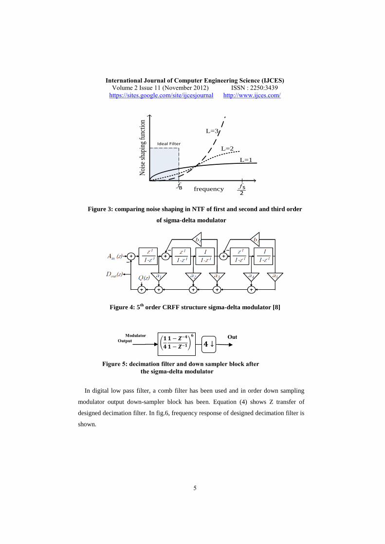
For designing sigma-delta loop filter, CRFF structure in fig4 has been chosen. NTF
zeroes of this structure are on unite circle (Z=1) and it makes density of output
modulator noise be decrease [8]. For canceling high frequency quantization noise from
modulator’s output and getting high resolution, modulator’s output must passed away
through decimation. Output modulator rate has been increased by over-sampling must
be decreased by down-sampler block after modulator, to nyquist rate. In fig 5 digital
low pass filter and down sampler block has been shown.
International Journal of Computer Engineering Science (IJCES)
Volume 2 Issue 11 (November 2012) ISSN : 2250:3439
https://sites.google.com/site/ijcesjournal http://www.ijces.com/
5
L=3
L=2
L=1
fB fs
2
Noi
se s
hapi
ng f
unct
ion
frequency
Ideal Filter
Figure 3: comparing noise shaping in NTF of first and second and third order
of sigma-delta modulator
Figure 4: 5th
order CRFF structure sigma-delta modulator [8]
In digital low pass filter, a comb filter has been used and in order down sampling
modulator output down-sampler block has been. Equation (4) shows Z transfer of
designed decimation filter. In fig.6, frequency response of designed decimation filter is
shown.
(
)
Out Modulator
Output
Figure 5: decimation filter and down sampler block after
the sigma-delta modulator

International Journal of Computer Engineering Science (IJCES)
Volume 2 Issue 11 (November 2012) ISSN : 2250:3439
https://sites.google.com/site/ijcesjournal http://www.ijces.com/
6
( ) (
)
( )
Figure 6: frequency response of decimation filter designed
3. Optimizing SIGMA-DELTA
3.1 Genetic Algorithm
GAs are search and optimization algorithms based on the mechanics of natural
selection and natural genetics. They make use of structured but randomized
information exchange and concept of the survival of the fittest. The algorithm starts
with an initial population which consists of a collection of chromosomes i.e. possible
solutions coded in the form of strings. The chromosome which produces the minimum
error function value represents the best solution. The chromosomes which represent the
better solutions are selected using roulette wheel selection technique. Genetic operators
like crossover, mutation, elitism etc. are applied over the selected chromosomes. As a
result a new set of chromosome is produced. This process is repeated until a fit
solution appears. In essence, a population of chromosomes is always available to get
the desired result. Occasionally a new part is added to a chromosome to make it more
robust. Genetic algorithms exploit past to extrapolate new search points to provide
improved performance. A robust method like GA works well across a wide range of
problems and also is more efficient. The traditional derivatives based approach,
-0.4 -0.3 -0.2 -0.1 0 0.1 0.2 0.3 0.4 0.5
-250
-200
-150
-100
-50
0
Decimation Filter
Frequence (* fs)
DB
(Am
plitu
de)

International Journal of Computer Engineering Science (IJCES)
Volume 2 Issue 11 (November 2012) ISSN : 2250:3439
https://sites.google.com/site/ijcesjournal http://www.ijces.com/
7
enumerative schemes and simple random walks are not that good for all classes of
problems. On the other hand, heuristics approaches, such as genetic algorithms (GAs),
differ from the traditional ones in that there exists a high probability that the global
optimal solution will be reached. Fig.7 shows the flowchart of the binary GA [7].
3.2 Using GA in ΣΔ ADC Design
In the design of ΣΔ ADCs, we need to optimize a large set of parameters including
the overall structures and the performance of the building blocks to achieve the
minimum density of noise in output and required signal-to-noise ratio. Therefore,
behavioral simulations were carried out using a set of Simulink models in MATLAB
Simulink environment in order to verify the performance The most important
parameter to be optimized in a sigma-delta modulator are the gain coefficients in order
to achieve the desired signal-to-noise ratio. GA is one of the best optimization
techniques which find a global optimum solution without taking much of the
computational power. The steps involved in the process of optimization using GA is
shown in Fig.7 In the first step genetic algorithm cost function or fitness has to be
calculated. The cost function is the density noise function of sigma-delta ADC output.
After defining the fitness, the gain coefficients have been defined as chromosome and
with considering linear and non linear condition, genetic algorithm has been started.
3.3 Calculating density noise of sigma-delta as fitness function
For calculating density noise of sigma-delta first step, noise transfer
function (NTF) of sigma-delta modulator must be calculated then
density of quantization noise from NTF must be calculated. NTF
transfer function of fig.4 is calculated by Meison rule:
(6)
( )
( )
( ) ( )

International Journal of Computer Engineering Science (IJCES)
Volume 2 Issue 11 (November 2012) ISSN : 2250:3439
https://sites.google.com/site/ijcesjournal http://www.ijces.com/
8
Figure 7: genetic algorithm stage [7]
( )
( )
( )
( )
( )
( )
( )
( )
( )
( )
( )
( ) ( )
∫ ( )| ( )|
⁄
⁄
( )
That ( ) is density of white noise in sigma-delta modulator and it is constant and

International Journal of Computer Engineering Science (IJCES)
Volume 2 Issue 11 (November 2012) ISSN : 2250:3439
https://sites.google.com/site/ijcesjournal http://www.ijces.com/
9
equal to
⁄ that is quantization step.
3.5 Considered genetic algorithm conditions
In all stage of genetic optimizing modulator loop filter must be stable and coefficient
gain must be determined that either density noise of sigma-delta be minimum or
modulator loop filter be remained stable. For remaining loop filter stable, poles of NTF
must be located in unique circle (Z=1) during the optimization.
3.6 Genetic algorithm result
After set all genetic algorithm settings in MATLAB and running it, it has gotten to
this point for gain coefficient:
{
After that, result is put in loop filter and result of modulator output can be shown.
4. SIMULATION RESULT
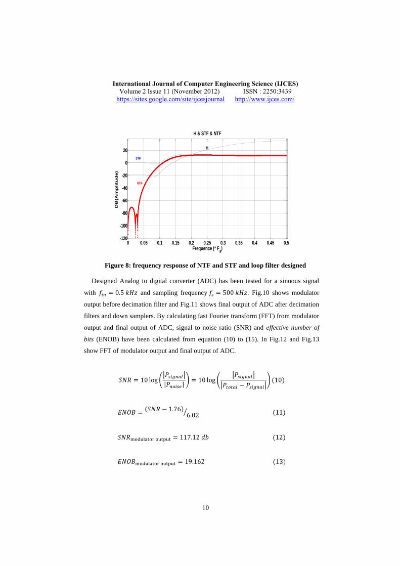
In fig.8 frequency response of NTF, STF and loop filter are shown for the loop filter’s
gain coefficients are obtained from genetic algorithm. Fig.9 shows zeros and poles of
NTF. As same as expected, NTF’s zeros are on unite circle (Z=1) and NTF’s poles are
in unite circle then filter is stable.
International Journal of Computer Engineering Science (IJCES)
Volume 2 Issue 11 (November 2012) ISSN : 2250:3439
https://sites.google.com/site/ijcesjournal http://www.ijces.com/
10
Figure 8: frequency response of NTF and STF and loop filter designed
Designed Analog to digital converter (ADC) has been tested for a sinuous signal
with and sampling frequency . Fig.10 shows modulator
output before decimation filter and Fig.11 shows final output of ADC after decimation
filters and down samplers. By calculating fast Fourier transform (FFT) from modulator
output and final output of ADC, signal to noise ratio (SNR) and effective number of
bits (ENOB) have been calculated from equation (10) to (15). In Fig.12 and Fig.13
show FFT of modulator output and final output of ADC.
(| |
| |) (
| |
| |) ( )
( )
⁄ ( )
( )
( )
0 0.05 0.1 0.15 0.2 0.25 0.3 0.35 0.4 0.45 0.5-120
-100
-80
-60
-40
-20
0
20
H & STF & NTF
Frequence (* Fs)
DB
(Am
plitu
de)
NTF
STF
H

International Journal of Computer Engineering Science (IJCES)
Volume 2 Issue 11 (November 2012) ISSN : 2250:3439
https://sites.google.com/site/ijcesjournal http://www.ijces.com/
11
Figure 9: poles and zeros of NTF of sigma-delta modulator designed
Figure 10: time response of sigma-delta modulator output
( )
( )
0.5
1
1.5
30
210
60
240
90
270
120
300
150
330
180 0
NTF

International Journal of Computer Engineering Science (IJCES)
Volume 2 Issue 11 (November 2012) ISSN : 2250:3439
https://sites.google.com/site/ijcesjournal http://www.ijces.com/
12
5. CONCLUSION
In this paper a five order sigma-delta analog to digital convertor (ADC) is designed
and optimized that density of quantization noise in ADC output be minimized then
SNR and ENOB be improved. For calculating density of quantization noise in ADC
output, quantization noise of sigma-delta modulator output has been considered. Then
final cost function calculated, has been optimized by genetic algorithm and gain
coefficients of loop filter have been calculated that density of quantization noise in
ADC has been minimized then SNR and ENOB has been improved.
A GA-based search engine is developed for the quick and easy design of sigma-
delta modulators. The genetic algorithm based search engine can effectively search for
solutions with different characteristics and enables tradeoffs between different designs
considerations. It has been successfully used to improve the performance of a fifth
order sigma-delta ADC
Figure 11: time response output of decimation and downs ampler block after
sigma-delta modulator
which is considered decimation and digital low pass filer after the sigma delta
modulator. The coefficients can be optimized using GA which results in extended
dynamic range. It has also been applied to a traditional fifth order feedback topology to
find peak SNR values with good stability.
In [8] loop filter gain coefficients have been optimized without considering
decimation and digital filter and down sampler block effects after the sigma-delta

International Journal of Computer Engineering Science (IJCES)
Volume 2 Issue 11 (November 2012) ISSN : 2250:3439
https://sites.google.com/site/ijcesjournal http://www.ijces.com/
13
modulator. Then final SNR and ENOB of [8] are:
( )
( )
Gain coefficient of [8] is presented below:
{
Then in this work 7 DB in SNR and more than 1 bit in ENOB have been improved.
Figure 12: FFT of sigma-delta modulator output
10-1
100
101
102
103
104
105
106
-300
-250
-200
-150
-100
-50
0PSD of the Output
Frequency [Hz]
PS
D [
dB
]

International Journal of Computer Engineering Science (IJCES)
Volume 2 Issue 11 (November 2012) ISSN : 2250:3439
https://sites.google.com/site/ijcesjournal http://www.ijces.com/
14
Figure 13: FFT of output of decimation and downs ampler block after sigma-
delta modulator
6. REFERENCE
[1]. Ramin Zanbaghi,Terri S. Fiez and Gabor Tem,New Zero-Optimization
Scheme for Noise-Coupled ΔΣ ADCs”, 978-1-4244-5309 IEEE, 2010
[2]. Christoph Zorn, Christian Widemann, Timon Br ¨ uckner, Maurits Ortmanns
and Wolfgang Mathis,” STF Optimization of 1-Bit CT SD Modulators Based
on Scaled Loop Filter Coefficients” 20th European Conference on Circuit
Theory and Design (ECCTD), 2011
[3]. Soren Hein, Avideh Zakhor, “Sigma-dela modulators nonlinear decoding
algorithms and stability analysis”, Kluwer , Boston,1993
[4]. Augusto Marques, Vincenzo Peluso, Michel S. Steyaert, IEEE, and Willy M.
Sansen, “Optimal Parameters for sigma-delta Modulator Topologies” IEEE
TRANSACTIONS ON CIRCUITS AND SYSTEMS—II: ANALOG AND
DIGITAL SIGNAL PROCESSING, VOL. 45, NO. 9, SEPTEMBER 1998
[5]. Lars Risbo, “On the Design of Tone-Free sigma-delta Modulators” IEEE
TRANSACTIONS ON CIRCUITS AND SYSTEMS-11: ANALOG AND
10-1
100
101
102
103
104
105
-300
-250
-200
-150
-100
-50
0PSD of the Output Decimation DOWNsampled
Frequency [Hz]
PS
D [
dB
]

International Journal of Computer Engineering Science (IJCES)
Volume 2 Issue 11 (November 2012) ISSN : 2250:3439
https://sites.google.com/site/ijcesjournal http://www.ijces.com/
15
DIGITAL SIGNAL PROCESSING, VOL. 42, NO. 1, JANUARY 1995
[6]. Gabriel V. Iana, Gheorghe Serban, Petre Anghelescu, Laurentiu Ionescu,”
Optimization of Sigma-Delta Modulator Based on Artificial Immune
Algorithms”, 12th International Conference on Optimization of Electrical and
Electronic Equipment, 2010
[7]. Ms.R.W.Jasutkar Dr.P.R.Bajaj Dr.A.Y.Deshmukh, “GA Based Low Power
Sigma Delta Modulator for Biomedical Applications”, 978-1-4244-9477-
IEEE, 2011
[8]. Robin Matthew Tsang, “High-Performance sigma-delta Analog-to-Digital
Conversion”, phd thesis, 2008
[9]. Sangil Park, "Principles of Sigma-Delta Modulation for Analog-to- Digital
Converters", Motorola Digital Signal Processors