5 Current Field Measurement 5.1Alternating Current Field Measurement 5.2Direct Current Potential...
27
5 Current Field Measurement 5.1 Alternating Current Field Measurement 5.2 Direct Current Potential Drop 5.3 Alternating Current Potential Drop
-
Upload
lawson-shady -
Category
Documents
-
view
235 -
download
1
Transcript of 5 Current Field Measurement 5.1Alternating Current Field Measurement 5.2Direct Current Potential...

5 Current Field Measurement
5.1 Alternating Current Field Measurement
5.2 Direct Current Potential Drop
5.3 Alternating Current Potential Drop

5.1 Alternating Current Field Measurement
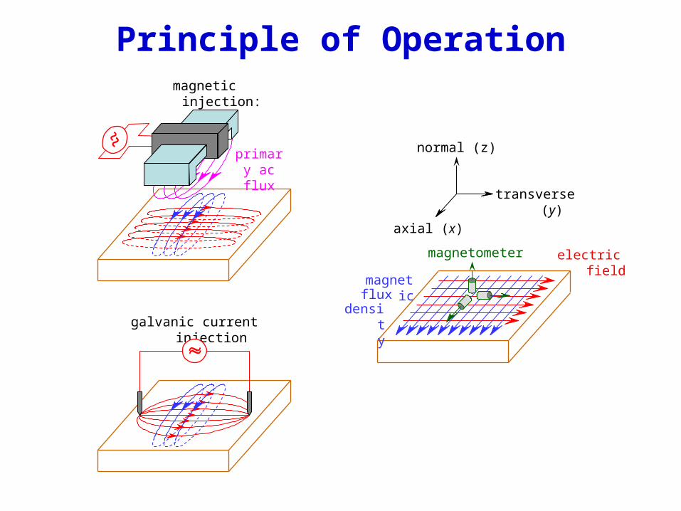
Principle of Operation
electric field
magneticflux
density
axial (x)
transverse (y)
normal (z)
galvanic current injection
magnetometer
magnetic injection:
primary ac flux
~~
Bx0
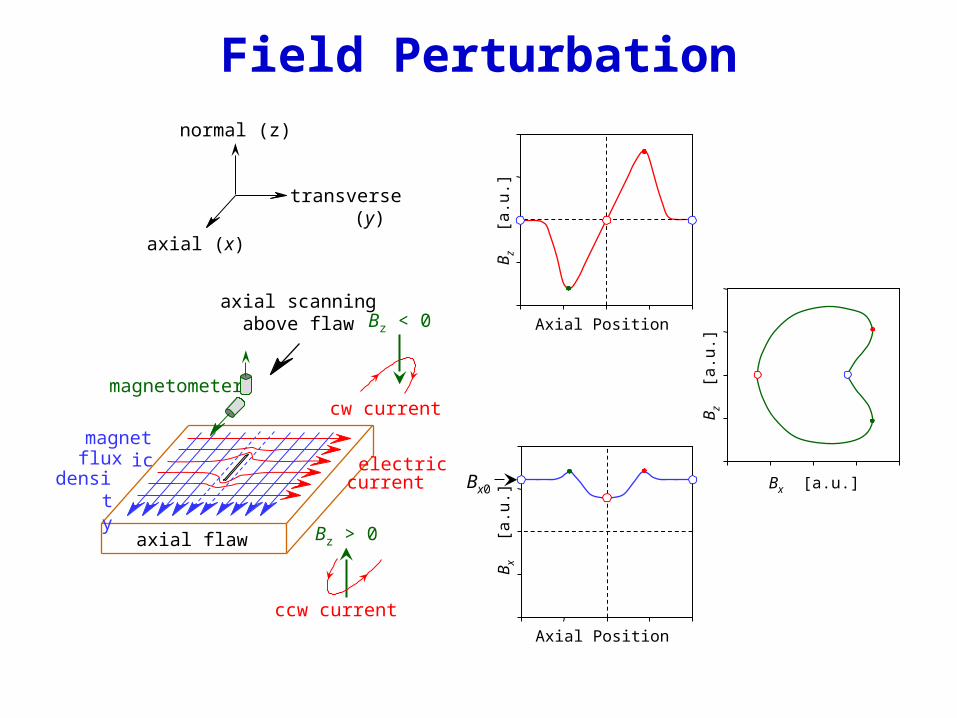
Field Perturbation
magneticflux
density
magnetometer
axial (x)
transverse (y)
normal (z)
axial flaw
cw current
Bz < 0
electriccurrent
Bz > 0
ccw current
axial scanningabove flaw Axial Position
Bz
[a.u
.]
Axial Position
Bx
[a.u
.]
Bz
[a.u
.]
Bx [a.u.]

Uniform Field
advantages:
testing through coatings
depth information
limited boundary effects
disadvantages:
reduced sensitivity
sensitivity to geometry
flaw orientation
effect of coating thickness on axial magnetic flux density Bx
(ferrous steel, 5 kHz, δ 0.25 mm, 30-mm-long solenoid)
8
7
6
5
4
3
2
1
00 5 10 15 20
Coating Thickness [mm]
ΔB
x [%
]
50 5 mm
20 2 mm
20 1 mm
slot size

30
25
20
15
10
5
0
Slot Depth [mm]
ΔB
x an
d Δ
Bz
[%]
0 0.5 1 1.5 2 2.5
Bx at 5 kHz
Bz at 5 kHz
Bx at 50 kHz
Bz at 50 kHz
Axial Flaw
8
7
6
5
4
3
2
1
00 10 20 30 40
Slot Depth [mm]
ΔB
xm p
er 1
mm
Slo
t Dep
th [
%]
40-mm-longsolenoid
12-mm-longsolenoid
rate of increase of the minimum of Bx with
slot depth at the center
2-mm-diameter coil, ferrous steel
changes normalized to Bx0
(parallel to B, normal to E)
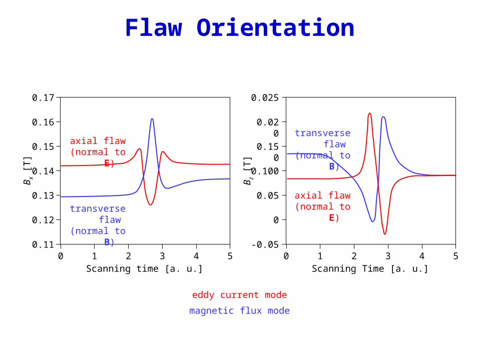
Flaw Orientation
0.17
0.16
0.15
0.14
0.13
0.12
0.11
Bx
[T]
0 1 2 3 4 5Scanning time [a. u.]
transverse flaw(normal to B)
axial flaw(normal to E)
0.025
0.020
0.150
0.100
0.05
0
-0.05B
z [T
]0 1 2 3 4 5
Scanning Time [a. u.]
transverse flaw(normal to B)
axial flaw(normal to E)
eddy current mode
magnetic flux mode
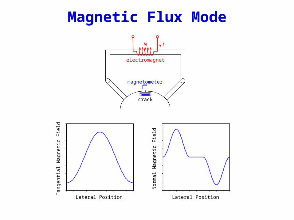
Magnetic Flux Mode
electromagnet
crack
N I
magnetometer
Lateral Position
Tan
gent
ial M
agne
tic
Fie
ld
Lateral Position
Nor
mal
Mag
neti
c F
ield

5.2 Direct Current Potential Drop
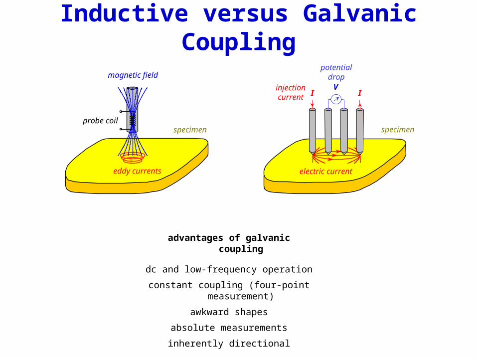
Inductive versus Galvanic Coupling
specimen
eddy currents
probe coil
magnetic field
electric current
VI I
injectioncurrent
potential drop
specimen
advantages of galvanic coupling
dc and low-frequency operation
constant coupling (four-point measurement)
awkward shapes
absolute measurements
inherently directional

Thin-Plate Approximation
combined electric current and potential field2a2b
t << a
( ) ( )2
IE r J r
r t
( ) ( )2r r
I drV r E r dr
t r
( ) ln const2
IV r r
t
( ) ( )V V V
lnI a b
Vt a b
2 ( ) ( )V V a b V a b
I (+) I (-)V (+) V (-)
I (+) I (-)
V (+) V (-)
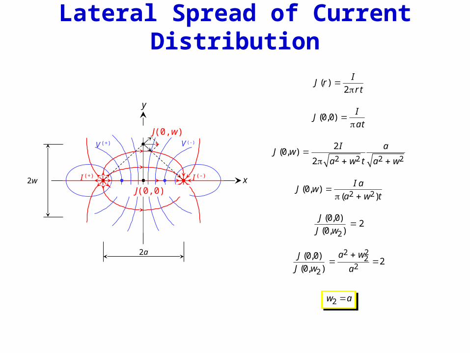
Lateral Spread of Current Distribution
( )2
IJ r
r t
(0,0)I
Jat
2 2 2 2
2(0, )
2
I aJ w
a w t a w
2 2(0, )
( )
I aJ w
a w t
2
(0,0)2
(0, )
J
J w
2 22
22
(0,0)2
(0, )
a wJ
J w a
2w a
2w I (+) I (-)
V (+) V (-)
x
y
2a
J(0,w)
J(0,0)

Thick-Plate Approximation
2( ) ( )
2
IE r J r
r
2( ) ( )
2r r
I drV r E r dr
r
( ) const2
IV r
r
t >> a
2a2b
I (+) I (-)V (+) V (-)
combined electric current and potential field
I (+) I (-)V (+) V (-)
( ) ( )V V V
1 1IV
a b a b
2 ( ) ( )V V a b V a b
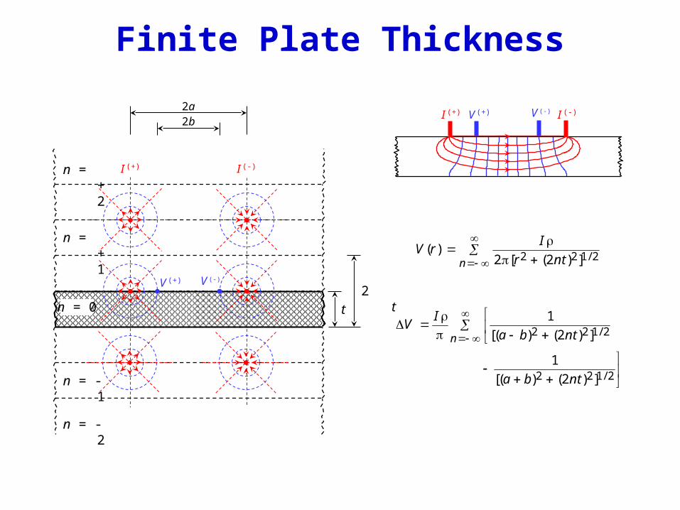
Finite Plate Thickness
2a2b
t
2 2 1/ 2( )
2 [ (2 ) ]n
IV r
r nt
2 2 1/ 2
2 2 1/ 2
1
[( ) (2 ) ]
1
[( ) (2 ) ]
n
IV
a b nt
a b nt
I (+) I (-)
V (+) V (-)
n = 0
n = -1
n = +1
n = -2
n = +2
2t
I (+) I (-)V (+) V (-)
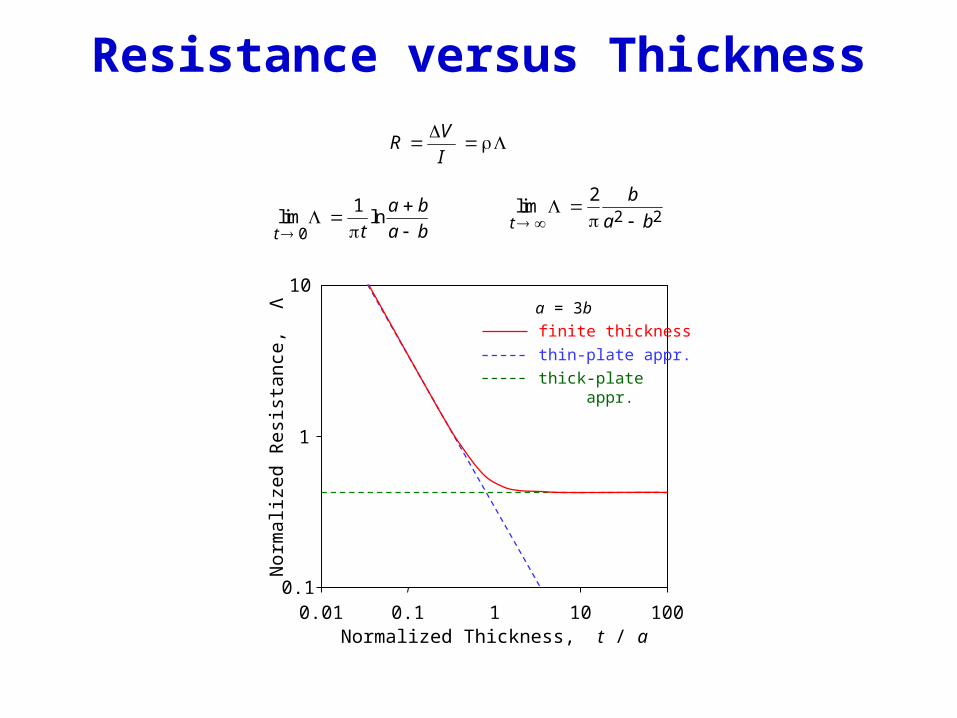
Resistance versus Thickness
0
1lim lnt
a b
t a b
2 2
2lim
t
b
a b
VR
I
0.1
1
10
0.01 0.1 1 10 100Normalized Thickness, t / a
Nor
mal
ized
Res
ista
nce,
Λ
finite thickness
thin-plate appr.
thick-plate appr.
a = 3b

Crack Detection by DCPD
intact specimen
I (+) I (-)V (+) V (-)
( ) ( )0V V V
t
I (+) I (-)V (+) V (-)
cracked specimen
( ) ( )cV V V
c
1
2
3
0 0.2 0.4 0.6 0.8 1Normalized Crack Depth, c / t
Nor
mal
ized
Pot
enti
al D
rop,
ΔV
c / Δ
V0
a / t =
0.441.21.8
a = 3b
infinite slot
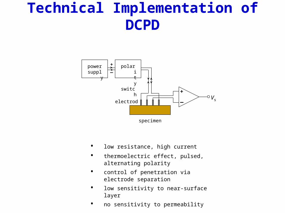
Technical Implementation of DCPD
• low resistance, high current
• thermoelectric effect, pulsed, alternating polarity
• control of penetration via electrode separation
• low sensitivity to near-surface layer
• no sensitivity to permeability
powersupply
polarityswitch
+
_
specimen
electrodesVs
+_

5.3 Alternating Current Potential Drop
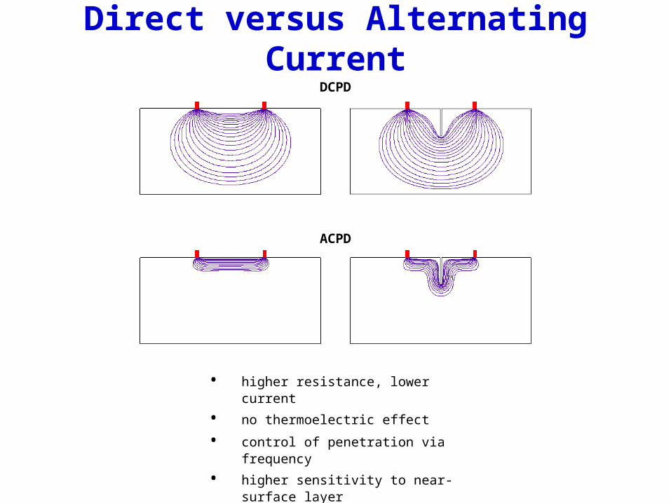
Direct versus Alternating CurrentDCPD
ACPD
• higher resistance, lower current
• no thermoelectric effect
• control of penetration via frequency
• higher sensitivity to near-surface layer
• sensitivity to permeability

Thin-Plate/Thin-Skin Approximation
0lim lnf
V a b
I t a b
2a2b
t << aI (+) I (-)V (+) V (-)
Re lnV a b
I T a b
min ,T t
f
lim Re lnf
V f a b
I a b

Skin Effect in Thin Nonmagnetic Plates
t( )f f t
t 20
1f
t
analytical prediction
a = 20 mm, b = 10 mm, t = 2 mm
100
101
102
103
100 101 102 103 104 105
Frequency [Hz]
Res
ista
nce
[µΩ
]
1 %IACS 2 %IACS 5 %IACS 10 %IAC
S
20 %IACS 50 %IACS
100 %IACS
ft
a = 20 mm, b = 10 mm, σ = 50 %IACS
0.05 mm0.1 mm0.2 mm0.5 mm
1 mm2 mm5 mm
ft100
101
102
103
100 101 102 103 104 105
Frequency [Hz]
Res
ista
nce
[µΩ
]
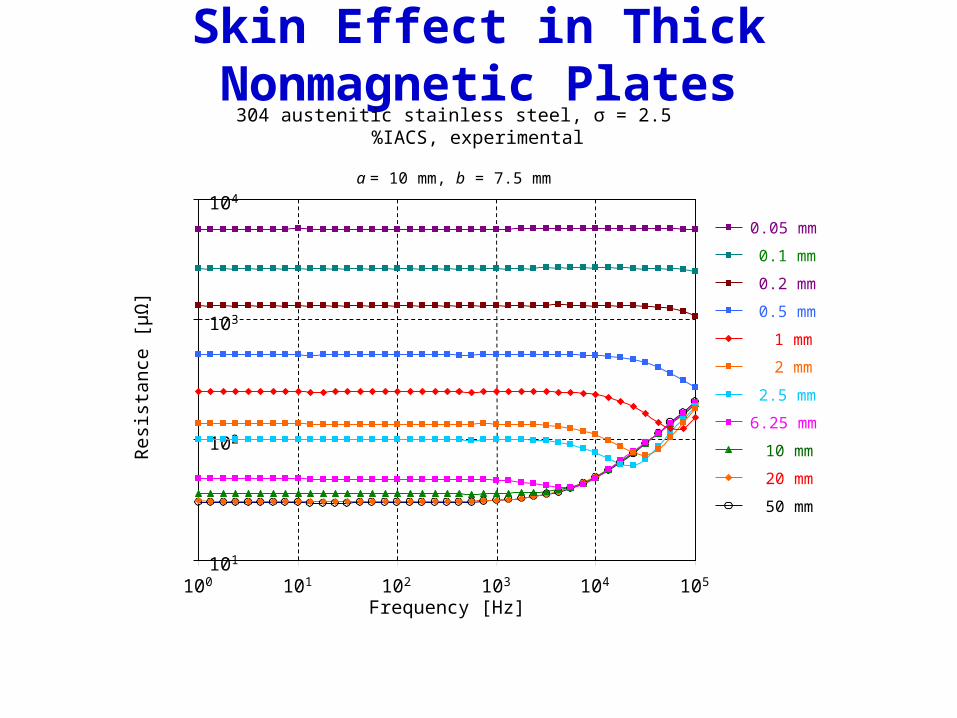
Skin Effect in Thick Nonmagnetic Plates304 austenitic stainless steel, σ = 2.5 %IACS, experimental
101
102
103
104
100 101 102 103 104 105
Frequency [Hz]
Res
ista
nce
[µΩ
]
50 mm
20 mm
10 mm
6.25 mm
2.5 mm
2 mm
1 mm
0.5 mm
0.2 mm
0.1 mm
0.05 mm
a = 10 mm, b = 7.5 mm
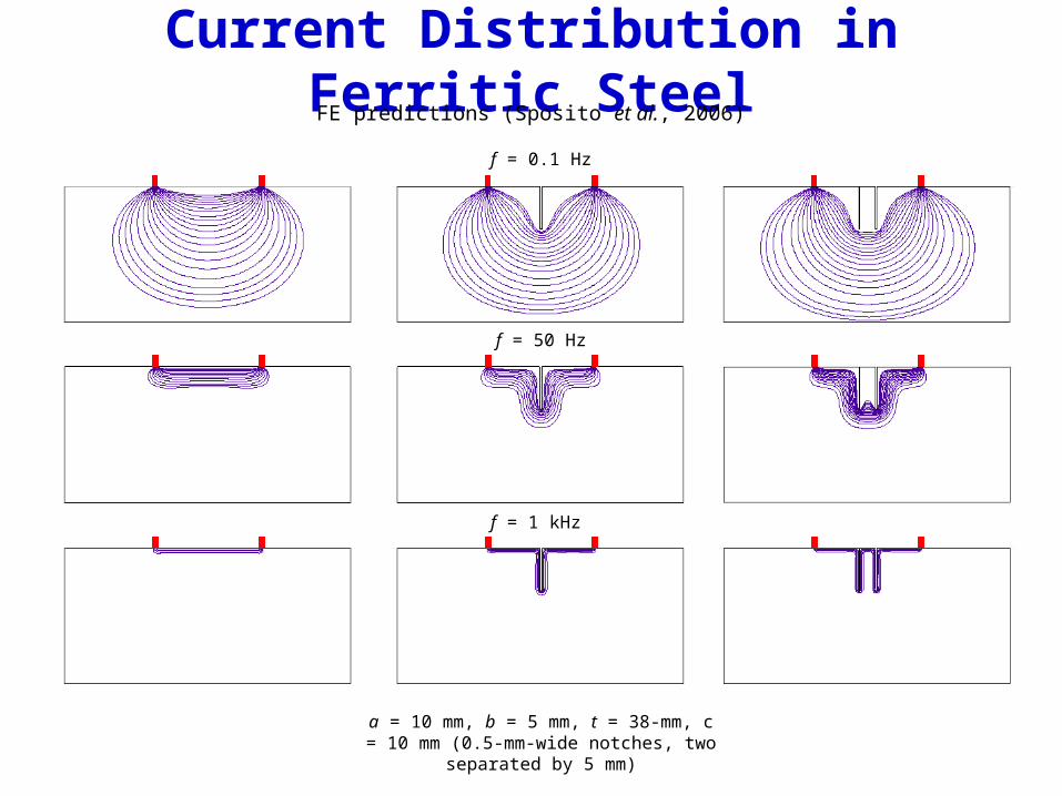
Current Distribution in Ferritic Steel
f = 0.1 Hz
FE predictions (Sposito et al., 2006)
f = 50 Hz
f = 1 kHz
a = 10 mm, b = 5 mm, t = 38-mm, c = 10 mm (0.5-mm-wide notches, two separated by 5 mm)
Thin-Skin Approximation
VZ R i X
I
c 0 c 0c
0 0
R RK
R
0 lna b
a b
c2
lna b c
a b
*0 0R R *
c cR R
0
1
2
1 2 3Electrode Shape Factor, a / b
Ele
ctro
de G
ain,
0
2b2a
2b2a
c
0 lna b
Ra b
2lnc
a b cR
a b
c0 0
1 2lim
c
cK
a b
* fR
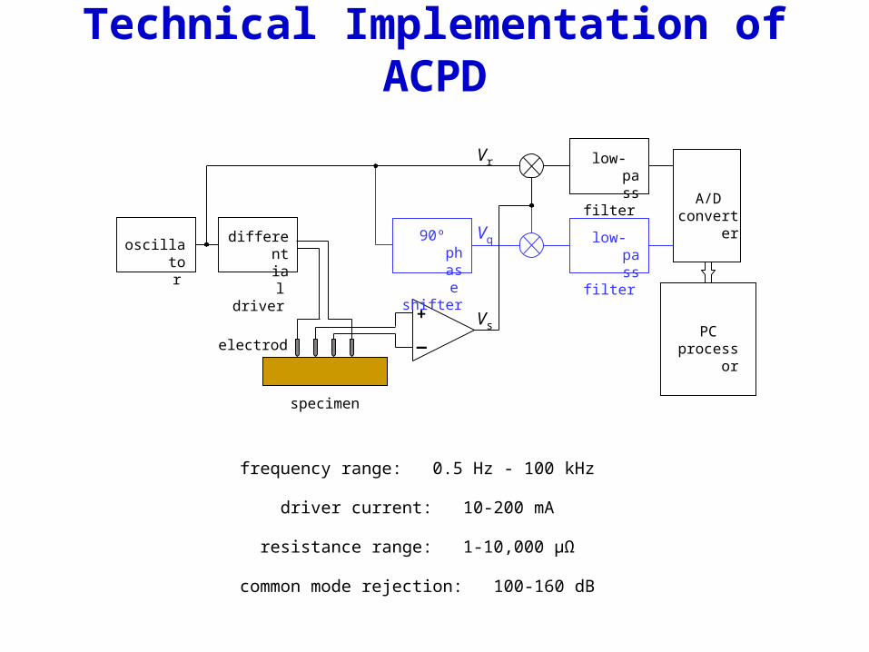
Technical Implementation of ACPD
low-passfilter
low-passfilter
oscillatordifferential
driver
+
_
90º phaseshifter
A/Dconverter
specimen
electrodesPC
processor
Vr
Vs
Vq
frequency range: 0.5 Hz - 100 kHz
driver current: 10-200 mA
resistance range: 1-10,000 µΩ
common mode rejection: 100-160 dB .

a = 0.160”
b = 0.080”
w = 0.054”
2 d = 0.120”
voltagesensing
currentinjection
welding
weldment
d
w
edge weld
clamshellcatalytic converter
Application Example: Weld Penetration
NDE [mil]
Fra
ctur
e S
urfa
ce [
mil
s]
0
10
20
30
40
50
60
70
80
0 10 20 30 40 50 60 70 80
weld penetration (w)
Weld Penetration [mil]
Res
ista
nce
[µΩ
]
0
50
100
150
200
0 20 40 60 80 100 120
b =
120 mils
80 mils100 mils
electrode separation (b)

Application Example: Erosion Monitoring
0 5 10 15 20Time [day]
20
21
22
23
24
25
Tem
pera
ture
[ºC
]
32.0
32.2
32.4
32.6
32.8
33.0R
esis
tanc
e [µ
Ω]
0 5 10 15 20Time [day]
20
21
22
23
24
25
Tem
pera
ture
[ºC
]
32.0
32.2
32.4
32.6
32.8
33.0
Res
ista
nce
[µΩ
]
erosionerosion
before compensation after compensation
β 0.001 [1/ºC]
0 0( ) [1 ( )]T T T
50
60
70
80
90
100
110
120
130
0 200 400 600 800Temperature [ºC]
Res
isti
vity
[µ
Ω c
m]
301 302 303 304 309 310 316 321 347 403
internalerosion/corrosion
pipe