Shunt-Based 200-A Peak Current Measurement … · Shunt-Based 200-A Peak Current Measurement...
28
5 V 2.5 V –2.5 V REF2033 3.3 V 1.65 V Isolation amplifier AMC1200 1.65 V (VREF) 3.3 V 2.5 V –2.5 V 0- to 3.3-V output interface to ADC Gain = 10 PWM rectifier 3-phase inverter M AC Single-line diagram of source connection Shunt TIDA-00445 OPA2376 OPA376 LM4040 SN6501 1 TIDUB91A – December 2015 – Revised March 2016 Submit Documentation Feedback Copyright © 2015–2016, Texas Instruments Incorporated Shunt-Based 200-A Peak Current Measurement Reference Design Using Isolation Amplifier TI Designs Shunt-Based 200-A Peak Current Measurement Reference Design Using Isolation Amplifier All trademarks are the property of their respective owners. TI Designs This TI Design provides a reference solution for isolated current measurement using shunt and isolated amplifiers. By limiting the shunt voltage to 25 mV, this design is able to reduce power dissipation in the shunt and achieves a high current measurement range of up to 200 A. Shunt voltage is further amplified by precision op amps in instrumentation amplifier-based configuration with a gain of 10 to match the input range of isolation amplifier. The output of isolation amplifier is level shifted and scaled to utilize the complete input range of 3.3-V ADC. This design uses free running transformer driver for generating isolated supply voltage for the high voltage side of the circuit. Small form factor for the power supply is achieved by the operation of driver at 400 kHz. Design Resources TIDA-00445 Design Folder AMC1200 Product Folder OPA2376 Product Folder OPA376 Product Folder REF2033 Product Folder SN6501 Product Folder LM4040 Product Folder ASK Our E2E Experts Design Features • Shunt-Based Isolated 200-A PK Current Measurement Solution • Limiting Shunt Voltage to 25 mV Lessens Power Dissipation • High-Side Current Sense Circuit With High Common-Mode Voltage of 1200-V PEAK , supporting up to 690-V AC Mains Powered Drives • Calibrated AC Accuracy of < 1% Across Temperatures –25°C to 85°C • Can Interface Directly With Differential or Single-Ended ADC • Small Form Factor Push Pull-Based Isolated Power Supply to Power High-Side Circuit • Built-in 1.65-V REF to Level Shift Output Featured Applications • Active Front-End Converters • UPS • Variable Speed Drives
-
Upload
nguyenkien -
Category
Documents
-
view
235 -
download
1
Transcript of Shunt-Based 200-A Peak Current Measurement … · Shunt-Based 200-A Peak Current Measurement...

5 V
2.5 V ±2.5 V
REF20333.3 V
1.65 V
Isolation amplifier
AMC1200
1.65 V(VREF)
3.3 V
2.5 V±2.5 V
0- to 3.3-V outputinterface to ADC
Gain = 10
PWM rectifier
3-phase inverter
MAC
Single-line diagram of source connection Shunt
TIDA-00445
OPA2376
OPA376
LM4040
SN6501
1TIDUB91A–December 2015–Revised March 2016Submit Documentation Feedback
Copyright © 2015–2016, Texas Instruments Incorporated
Shunt-Based 200-A Peak Current Measurement Reference Design UsingIsolation Amplifier
TI DesignsShunt-Based 200-A Peak Current Measurement ReferenceDesign Using Isolation Amplifier
All trademarks are the property of their respective owners.
TI DesignsThis TI Design provides a reference solution forisolated current measurement using shunt and isolatedamplifiers. By limiting the shunt voltage to 25 mV, thisdesign is able to reduce power dissipation in the shuntand achieves a high current measurement range of upto 200 A. Shunt voltage is further amplified byprecision op amps in instrumentation amplifier-basedconfiguration with a gain of 10 to match the inputrange of isolation amplifier. The output of isolationamplifier is level shifted and scaled to utilize thecomplete input range of 3.3-V ADC. This design usesfree running transformer driver for generating isolatedsupply voltage for the high voltage side of the circuit.Small form factor for the power supply is achieved bythe operation of driver at 400 kHz.
Design Resources
TIDA-00445 Design FolderAMC1200 Product FolderOPA2376 Product FolderOPA376 Product FolderREF2033 Product FolderSN6501 Product FolderLM4040 Product Folder
ASK Our E2E Experts
Design Features• Shunt-Based Isolated 200-APK Current
Measurement Solution• Limiting Shunt Voltage to 25 mV Lessens Power
Dissipation• High-Side Current Sense Circuit With High
Common-Mode Voltage of 1200-VPEAK, supportingup to 690-V AC Mains Powered Drives
• Calibrated AC Accuracy of < 1% AcrossTemperatures –25°C to 85°C
• Can Interface Directly With Differential orSingle-Ended ADC
• Small Form Factor Push Pull-Based Isolated PowerSupply to Power High-Side Circuit
• Built-in 1.65-VREF to Level Shift Output
Featured Applications• Active Front-End Converters• UPS• Variable Speed Drives

System Description www.ti.com
2 TIDUB91A–December 2015–Revised March 2016Submit Documentation Feedback
Copyright © 2015–2016, Texas Instruments Incorporated
Shunt-Based 200-A Peak Current Measurement Reference Design UsingIsolation Amplifier
An IMPORTANT NOTICE at the end of this TI reference design addresses authorized use, intellectual property matters and otherimportant disclaimers and information.
1 System DescriptionCurrent measurement is an inherent part of any inverter-driven application such as motor control, UPS,active front-end (AFE) converters, and so on. Motor control algorithms like vector control and direct torquecontrol require current sensing for control purposes. Active front-end converters also measure grid currentto ensure they are in phase with voltage. Current measurement in UPS is used to control the batterycharging current as well as inverter operation and overload protection.
AFE converters are often used in high-performance adjustable speed drives (ASDs) where frequentacceleration and de-acceleration is required. AFE converters have many advantages like constant DCvoltage, fast dynamic response, unity power factor, low harmonic distortion, and bidirectional power flow.Generally, two control methods have been proposed for PWM rectifiers: Voltage-oriented control (VOC)and direct power control (DPC). The main goal of these control techniques is to reduce the currentharmonic and to regulate the DC bus voltage.
For normal operation, AFE requires three kinds of sensors to detect AC voltages, AC currents, and DCvoltage. A DC voltage sensor is demanded for the DC voltage feedback control and excessive voltageprotection. The two AC voltage sensors are needed to detect the phase angle of the source voltage, whichis taken as a reference frame of the controller, and thus to perform input power factor control. The two linecurrent sensors are required for the input current control for boosting action and excessive currentprotection. Alternatively, the single current sensor technique of PWM inverters can be applied to the AFE,where the phase currents are reconstructed using the measured DC link currents and the switching statesof the PWM inverter. Current sensor locations in the AFE are depicted in Figure 1.
Figure 1. Current Sensor Locations in AFE
Multiple solutions exist today to measure current like Hall, flux gate sensors, current transformers, andshunt. Magnetic-based solutions inherently offer isolation benefits and have the capability to measurehigher currents. However, magnetic-based solutions can be expensive. The shunts are usually limited tomeasure currents less than 50 A owing to higher power dissipation. This TI Design provides a low-costsolution to enhance current measurement range using a 125-μΩ shunt up to 200 APK with isolationamplifier and signal conditioning circuit. The voltage across the shunt is limited to 25 mV, which issubsequently amplified to 250 mV by a gain stage before fed to the isolation amplifier. The completecircuit design with simulation and test results are covered in this design guide. The current measurementrange can be further enhanced by reducing the value of the shunt.

www.ti.com Key System Specifications
3TIDUB91A–December 2015–Revised March 2016Submit Documentation Feedback
Copyright © 2015–2016, Texas Instruments Incorporated
Shunt-Based 200-A Peak Current Measurement Reference Design UsingIsolation Amplifier
2 Key System Specifications
Table 1. Key System Specifications
PARAMETER SPECIFICATIONMaximum current 200 APK
Current type AC and DCCommon-mode voltage 1200 VPK
Calibrated accuracy < 1%Common-mode transient immunity 15 kV/µsOutput 150 mV to 3.15 VOperating ambient temperature –25°C to 85°CFeatures Isolated current sense outputs designed to be interfaced to 3.3-V built-in ADCs of MCUs

5 V
2.5 V ±2.5 V
REF20333.3 V
1.65 V
Isolation amplifier
AMC1200
1.65 V(VREF)
3.3 V
2.5 V±2.5 V
0- to 3.3-V outputinterface to ADC
Gain = 10
PWM rectifier
3-phase inverter
MAC
Single-line diagram of source connection Shunt
TIDA-00445
OPA2376
OPA376
LM4040
SN6501
Block Diagram www.ti.com
4 TIDUB91A–December 2015–Revised March 2016Submit Documentation Feedback
Copyright © 2015–2016, Texas Instruments Incorporated
Shunt-Based 200-A Peak Current Measurement Reference Design UsingIsolation Amplifier
3 Block DiagramThe block diagram for current measurement using shunt is shown in Figure 2. The main parts of thisdesign consists of gain stage succeeding shunt using a precision op amp (OPA2376), an isolationamplifier (AMC1200), and a differential to single-ended conversion using the OPA376.
Figure 2. Block Diagram for Current Measurement Using Shunt
The front-end gain stage is designed using the OPA2376 in instrumentation amplifier topology enabling itto accept differential input and have differential output. The overall gain of this stage is set to 10 foramplifying the ±25 mV across the shunt to ±250 mV to fit the input range of the isolation amplifier. TheOPA2376 is supplied with ±2.5 V.
The next stage involves the AMC1200, which provides galvanic isolation of up to 4000 VPEAK between thehigh-voltage and low-voltage circuit. It has a fixed internal gain of 8 and accepts a maximum input of±250 mV to operate in a linear region. It is powered on the high-voltage side by ±2.5 V and on the low-voltage side by 3.3 V, thus giving a differential output at a common-mode voltage of 1.29 V. This common-mode voltage can either be given directly to differential ADC or to next level shifter stage.
The output of isolation amplifier is fed to level shifter circuit. This circuit converts the differential outputfrom the AMC1200 to a single-ended signal along with level shift to match the input range of the single-ended ADC. This is achieved using the precision op amp OPA376, and the final output is mapped on to0 to 3.3 V. This op amp is powered using 3.3 V with a reference voltage of 1.65 V for level shifting.
The power supply circuit consists of the REF2033 and the SN6501.
The REF2033 derives 3.3 and 1.65 V from a 5-V supply. 3.3 V is used to power the OPA376 and the low-voltage side of the AMC1200. 1.65 V is used for as a reference voltage for the OPA376 to map output ofisolation amplifier to0 to 3.3 V.
The SN6501 drives the transformer to generate an isolated power supply for powering the high-voltageside of the circuit consisting of the front-end gain stage and the high side of the AMC1200. It is poweredfrom the 5-V input supply.

www.ti.com Block Diagram
5TIDUB91A–December 2015–Revised March 2016Submit Documentation Feedback
Copyright © 2015–2016, Texas Instruments Incorporated
Shunt-Based 200-A Peak Current Measurement Reference Design UsingIsolation Amplifier
3.1 Highlighted ProductsThis TIDA-00445 reference design features the following devices, which were selected based on theirspecifications. The key features of the highlighted products are mentioned as follows. For moreinformation on each of these devices, see their respective product folders at http://www.ti.com or click onthe links for the product folders on the first page of this reference design.
3.1.1 OPA376, OPA2376The OPA376 family represent a new generation of low-noise operational amplifiers with e-trim, offeringoutstanding AC precision and AC performance. Rail-to-rail input and output, low offset (25 μV max), lownoise (7.5 nV/√Hz), quiescent current (950 μA max), and a 5.5-MHz bandwidth make this part veryattractive for a variety of precision and portable applications.
In this design, the OPA2376 works as an instrumentation amplifier for the front-end gain stage and in levelshifter circuit.
This op amp was chosen for this design for its extremely low voltage offset, low temperature drift, rail-to-rail output, low noise, and low cost.
3.1.2 AMC1200The AMC1200 is a precision isolation amplifier with an output separated from the input circuitry by asilicon dioxide (SiO2) barrier that is highly resistant to magnetic interference. This barrier has been certifiedto provide galvanic isolation of up to 4000 VPEAK according to VDE-V 0884-10 and UL1577. Used inconjunction with isolated power supplies, this device prevents noise currents on a high common-modevoltage line from entering the local ground and interfering with or damaging sensitive circuitry.
The excellent performance of this device supports accurate current control resulting in system level powersaving and especially in motor control applications, lower torque ripple.
The AMC1200 is used in this design to provide galvanic isolation between the high and low voltage sides.It was selected mainly because of its very high transient immunity (10 kV/μs min), very low non-linearity(0.075 % max), and very low offset error.
3.1.3 REF2033Applications with only a positive supply voltage often require additional stable voltage in the middle of theADC input range to bias input bipolar signals. The REF2033 provides a reference voltage for the ADC anda second highly accurate voltage that can be used to bias the input bipolar signals.
The REF2033 offers excellent temperature drift (8 ppm/°C, max) and initial accuracy (0.05%) on both theVREF and VBIAS outputs while operating at a quiescent current less than 430 μA. In addition, the VREF andVBIAS outputs track each other with a precision of 6 ppm/°C (max) across the temperature range of –40°Cto 85°C. All these features increase the precision of the signal chain and decrease board space, whilereducing the cost of the system as compared to a discrete solution. Both the VREF and VBIAS have the sameexcellent specifications and can sink and source current equally well. Very long-term stability and low-noise levels make these devices ideally suited for high-precision industrial applications.
The REF2033 is used for its dual outputs in very small package, very low drift in output with temperature,and for its VREF and VBIAS tracking for higher accuracy.
3.1.4 SN6501The SN6501 is a monolithic oscillator and power driver, specifically designed for small form factor, isolatedpower supplies in isolated interface applications. The device drives a low-profile, center-tappedtransformer primary from a 3.3- or 5-V DC power supply. The secondary can be wound to provide anyisolated voltage based on transformer turns ratio.
This device includes an oscillator that feeds a gate-drive circuit. The gate-drive, comprised of a frequencydivider and a break-before-make (BBM) logic, provides two complementary output signals that alternatelyturn the two output transistors on and off with a duty cycle of 50%.
The SN6501 is used in this design for its isolated power supply to power the AMC1200 high-voltage sideand first gain stage.

System Design Theory www.ti.com
6 TIDUB91A–December 2015–Revised March 2016Submit Documentation Feedback
Copyright © 2015–2016, Texas Instruments Incorporated
Shunt-Based 200-A Peak Current Measurement Reference Design UsingIsolation Amplifier
4 System Design TheoryThis section details the design procedure for each circuit section.
4.1 Selection of Shunt ResistorThe value of the shunt resistor is chosen to have a 25-mV drop across it while the 200-A current is flowingthrough it, leading to 125 μΩ. The minimum power handling capability of the shunt must be 5 W. Fortesting purpose, two 250-μΩ resistors (CSS2725FTL250CT from Stack pole Electronics) were connectedin parallel with each having a 125-A current capability and 4-W dissipation. Other important parametersinclude the resistance tolerance, the temperature coefficient of resistance, low thermal EMF, and lowinductance.
4.2 Front-End Gain Stage With Isolation Amplifier
4.2.1 Gain Stage Using OPA2376This design is aimed to measure current as high as 200-A DC or 200-A peak-to-peak AC with a maximumdrop of 25 mV across the shunt. The major requirement of this particular stage is to provide an amplifieddifferential output to match the input (250 mV) of the isolation amplifier.
The individual op amp gains are set to 5, leading to a total gain of 10. Because the outputs are differential,each op amp provides an output of ±125 mV out of phase with each other by 180°. This is achieved by theconfiguration shown in Figure 3, which resembles instrumentation amplifier configuration:
Figure 3. Configuration to Get Differential Output
G
G
R14 R1 4R
R= ® =
X
G
R1V V1 1
R
æ ö= +ç ÷
ç ÷è ø
( ) ( )G
G
I R1 R IR2
R1 R R2
+ = - -
+ =
( )X G
Y
V I R1 R
V IR2
= +
= -
X YV V= -
X Y
G
R1 R2V V V1 1
R
æ ö+- = +ç ÷
ç ÷è ø
( )
( )
X Y G
G
X Y
G
V1 V2V V R1 R R2
R
R1 R2V V V1 V2 1
R
-- = + +
æ ö+- = - +ç ÷
ç ÷è ø
G
V1 V2I
R
-
=
( )X G Y
X Y G
V IR1 IR IR2 V 0
V V I R1 R R2
- - - - =
- = + +
www.ti.com System Design Theory
7TIDUB91A–December 2015–Revised March 2016Submit Documentation Feedback
Copyright © 2015–2016, Texas Instruments Incorporated
Shunt-Based 200-A Peak Current Measurement Reference Design UsingIsolation Amplifier
The voltage drop across the shunt is given to positive terminals of both op amps shown in Figure 3.Applying KVL to the loop VX – R1 – RG – R2 – VY:
(1)
Here, I is given as Equation 1 now becomes:
(2)
In this design, V2 is grounded with the high-voltage side ground of the board. Thus, considering V2 to beat ground potential with respect to V1:
Since the design needs a differential output that can directly be given to isolation amplifier, VX and VY mustbe equal and opposite of each other:
(3)
Again referring to Figure 3, if V2 is considered at ground potential, VX and VY now become
According to Equation 3:
(4)
Equation 4 shows one of the constraints for choosing the values of resistors. To provide an overall gain of10, each individual op amp has to provide a gain of 5 so that both the inputs to isolation amplifier areequal and opposite.
Again looking at Figure 3, considering V2 to be at ground potential, U2 is behaving like a non-invertingamplifier having transfer function:
To have a gain of 5:
(5)
From Equation 4 and Equation 5, R2 = 5 RG.
In order to limit the gain error, 0.1% accurate resistors are chosen. The choices of feedback resistors arerestricted to less than 10 kΩ to reduce the impact of noise voltages. Based on availability and accuracyneeded, the values chosen for this design are RG = 1.27 kΩ, R1 = 5.1 kΩ, and R2 = 6.34 kΩ.

5.10k
R8
1.27kR9
6.34k
R7
VCC
VEE
GND1
GND1
0.1µF
C6
0.1µF
C4
0R3
GND1
TP3
TP4
TP6
1
2
J1
1725656
0.22µFC3
18
R1
18
R2
1
3
2
48
U3A
OPA2376AID
7
5
6
48
U3BOPA2376AID
System Design Theory www.ti.com
8 TIDUB91A–December 2015–Revised March 2016Submit Documentation Feedback
Copyright © 2015–2016, Texas Instruments Incorporated
Shunt-Based 200-A Peak Current Measurement Reference Design UsingIsolation Amplifier
The simulation results using TINA-TI for this particular section are shown in Figure 4. All TINA-TI modelscan be found on the respective device product folders.
Figure 4. Simulation Result of Gain Stage
• VSHUNT is the voltage across shunt• VX is the output of upper op amp in the schematic• VY is the output of lower op amp in the schematic• VDIFF_OUTPUT is the output of this gain stage.
An RC filter of 20-kHz cut-off frequency is added before the gain stage to avoid entry of any highfrequency noise into the circuit. This filter can be changed according to the requirements of bandwidthversus noise immunity. The schematic for this stage is shown in Figure 5.
Figure 5. First Gain Stage
Connector J1 is used to connect the front-end stage with the shunt. The output of this gain stage is fed toisolation amplifier through the RC filter.

www.ti.com System Design Theory
9TIDUB91A–December 2015–Revised March 2016Submit Documentation Feedback
Copyright © 2015–2016, Texas Instruments Incorporated
Shunt-Based 200-A Peak Current Measurement Reference Design UsingIsolation Amplifier
4.2.2 Isolation AmplifierThis design uses the AMC1200 to provide galvanic isolation between the high- and low-voltage sides. TheAMC1200 provides a fixed gain of 8 along with level shifting the output. The high-voltage side is to bepowered by 5 V while the low-voltage side can be powered either by 5 V or 3.3 V depending on the levelshift of the output required.
This design uses ±2.5 V to power the high-voltage side and 3.3 V to power the low-voltage side. A TINAsimulation model for the isolation amplifier along with gain stage is shown in Figure 6. Here,VDIFF_OUTPUT = ±250 mV, where VDIFF_OUTPUT is the output of gain stage which is given to isolation amplifier,and VISO_OUT = ±250 mV × 8 = ±2 V, where VISO_OUT is the output of isolation amplifier.
Figure 6. TINA Model of Isolation Amplifier and First Gain Stage
In Figure 6, a current of 200 A is passed through a resistor of 125 μΩ, resulting in a voltage drop of25 mV, which is amplified 10 times and given to the isolation amplifier. The output of both stages areshown as simulation results in Figure 7.
Figure 7. Simulation Result of Isolation Amplifier
5.10k
R8
1.27kR9
6.34k
R7
V3.3
GND2
VCC
VEE
VEE
VCC
GND1
GND1
GND1
GND1
GND2
0.1µF
C6
0.1µF
C4
0.1µF
C7
0.1µF
C9
0.1µF
C8
VINP
VINN
0R3
GND1
TP3
TP4
TP7
TP5
TP9
TP10
TP6
1
2
J1
1725656
0.22µFC3
18
R1
18
R2
1
2
3
4
5
6
7
8
+
-
V+
V-
V-
V+
U4
AMC1200BDWV
12.0
R16
12.0
R17 330pF C18
12.0
R18
12.0
R19
330pFC19
1
3
2
48
U3A
OPA2376AID
7
5
6
48
U3BOPA2376AID
System Design Theory www.ti.com
10 TIDUB91A–December 2015–Revised March 2016Submit Documentation Feedback
Copyright © 2015–2016, Texas Instruments Incorporated
Shunt-Based 200-A Peak Current Measurement Reference Design UsingIsolation Amplifier
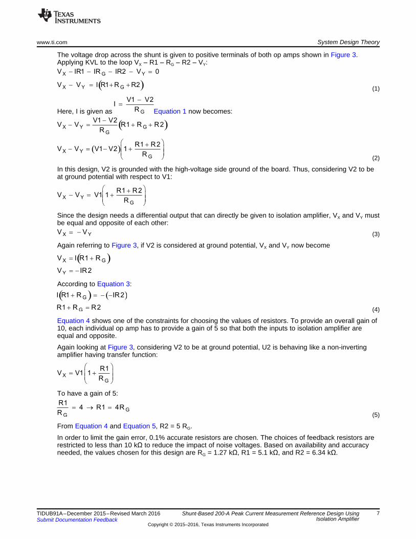
The schematic for this circuit is shown in Figure 8.
Figure 8. Isolation Amplifier Along With Front-End Amplifier
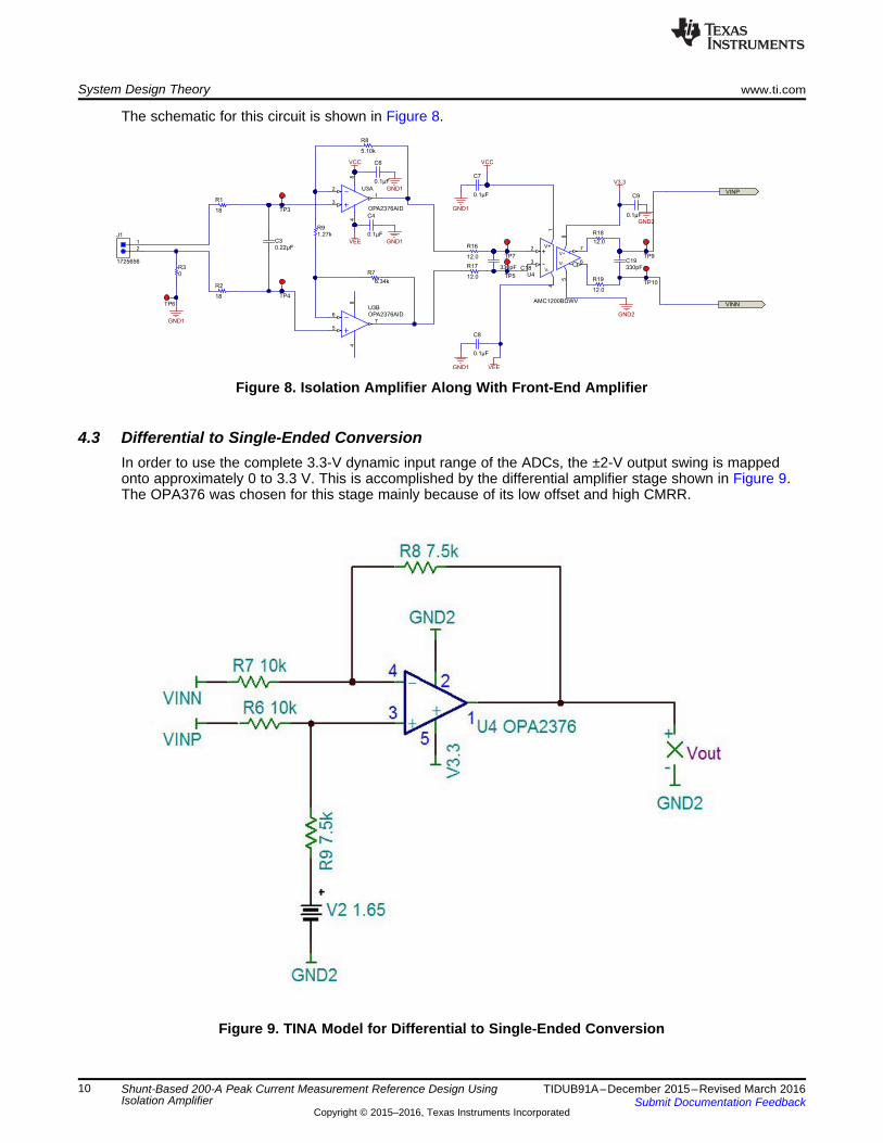
4.3 Differential to Single-Ended ConversionIn order to use the complete 3.3-V dynamic input range of the ADCs, the ±2-V output swing is mappedonto approximately 0 to 3.3 V. This is accomplished by the differential amplifier stage shown in Figure 9.The OPA376 was chosen for this stage mainly because of its low offset and high CMRR.
Figure 9. TINA Model for Differential to Single-Ended Conversion

( )R131.5 2
R11
R130.75
R11
æ ö= ç ÷
è ø
=
( )R13
Max swing allowed VINP VINNR11
= -
( )OUT REF
R13V VINP VINN V
R11
æ ö= - +ç ÷
è ø
www.ti.com System Design Theory
11TIDUB91A–December 2015–Revised March 2016Submit Documentation Feedback
Copyright © 2015–2016, Texas Instruments Incorporated
Shunt-Based 200-A Peak Current Measurement Reference Design UsingIsolation Amplifier
The transfer function for this circuit can be derived easily considering R13 = R12 and R11 = R10 (seeFigure 11) and using only two variables for them. The transfer function turns out to be:
(6)
Here, VREF is 1.65 V.
The OPA376 output voltage swing is limited up to 10 mV from the rails typically and 20 mV overtemperature. Considering the mismatch in resistor values, the output voltage is designed to be limited to alittle over 100 mV from the rails.
The ±2-V input to the differential amplifier is to be mapped onto nearly 0 to 3.3 V with 1.65 VREF. Providinga window of 150 mV from the rails, the maximum swing of output becomes 0.15 to 3.15 V. As a result, thepositive and negative swing that is allowed is 3.15 V – 1.65 V = 1.5 V riding over 1.65 VREF.
Thus, the ratio of resistors needed to achieve this shift is calculated as given:
(7)
To have a margin of 150 mV from the rails, chosen values are R13 = 7.5 kΩ and R11 = 10 kΩ; Thesimulation result with the output of this differential amplifier is shown in Figure 10.
Figure 10. Simulation Result for Differential to Single-Ended Converter
Here, VISO_OUT is the output of the AMC1200 as depicted in Figure 10, and VOUT is the final output of levelshifter. The schematic of the level shifter is shown in Figure 11.

GND2
V3.3
V1.65
GND2
0.1µF
C15
VINP
VINN
GND2
GND2
1
2345
J3142-0701-201
TP13
0.22µFC17
36
R1420.0k
R11
20.0kR10
14.7k
R13
14.7kR12
1
2
3
4
5
U7OPA376AIDBVR
System Design Theory www.ti.com
12 TIDUB91A–December 2015–Revised March 2016Submit Documentation Feedback
Copyright © 2015–2016, Texas Instruments Incorporated
Shunt-Based 200-A Peak Current Measurement Reference Design UsingIsolation Amplifier
Figure 11. Differential Amplifier Stage
To compare the overall performance and linearity of the circuit, the transfer function is plotted for inputcurrent versus output of every stage separately as shown in Figure 12.
Figure 12. Transfer Function Plotted Using TINA

GND2
GND2
P5V
61
3
5
4
2
T1
750342879
D11
VCC2
D23
GND4
GND5
U5
SN6501DBVR
0.1µF
C11
GND2
GND1
VEE
1: 3.5VCC
TP1
TP2
Green
12
D1
10µFC5
D3
MBR0540T1G
D2
MBR0540T1G
1µFC1
1µFC2
NC
U2
LM4040BIM3-2.5
NC
U1
LM4040BIM3-2.5
576R6
576R5
10µFC14
1.00kR4
( )T min
5.5 VV 9.1 Vµs
2 300 kHz³ =
´
( ) ( )( ) ( )
( )IN max
T min IN max
VT maxV V
2 2 f min³ ´ =
´
www.ti.com System Design Theory
13TIDUB91A–December 2015–Revised March 2016Submit Documentation Feedback
Copyright © 2015–2016, Texas Instruments Incorporated
Shunt-Based 200-A Peak Current Measurement Reference Design UsingIsolation Amplifier
4.4 Power Supply and Reference Solution
4.4.1 Isolated Power SupplyThe AMC1200 requires an isolated power supply for powering its input section. The SN6501 is used as aswitching device to generate a 5-V isolated output and drives transformer.
The SN6501 is a monolithic oscillator and power-driver, specifically designed for isolated power suppliesin isolated interface applications with a small form factor. It drives a low-profile, center-tapped transformerprimary from a 3.3- or 5-V DC power supply. The SN6501 consists of an oscillator followed by a gate drivecircuit that provides the complementary output signals to drive the ground referenced N-channel powerswitches. The internal logic ensures break-before-make action between the two switches.
The SN6501 features:• Push-pull driver for small transformers• Single 3.3- or 5-V supply
While selecting the transformer, it is important to prevent transformer from saturation. To achieve this, thetransformer’s V-t product must be greater than the maximum V-t product applied by the SN6501. Themaximum voltage delivered by the SN6501 is the nominal converter input plus 10%. The maximum timethis voltage is applied to the primary is half the period of the lowest frequency at the specified inputvoltage. Therefore, the transformer’s minimum V-t product is determined through:
(8)
Common V-t values for low-power center-tapped transformers range from 22 to 150 Vμs with typicalfootprints of 10 × 12 mm.
This design needs to sense bipolar signal using a unipolar power supply. The front-end amplifier shouldbe able to take negative as well as positive inputs. Thus it is necessary to power it using a dual supply.Therefore, after rectifying the output of the transformer, we have to split it to get ±2.5 V. This is achievedusing zener diodes as seen in Figure 13.
Figure 13. Isolated Power Supply
VCC and VEE as shown in Figure 13 are used to power the first gain stage as well as the high-voltage sideof isolation amplifier. The turn’s ratio of chosen transformer is 1:3.5. Thus, for a 5-V primary input voltage,the secondary voltage is 17.5 V. After accounting for the forward voltage drop of the diodes, the voltageavailable after rectification is around 16.5 V.

VBIAS1
GND2
EN3
VIN4
VREF5
U6
REF2033AIDDCR
V3.3
V1.65
GND2
P5V
GND2
0.1µF
C12
GND2
0.1µFC10
0.1µFC16
GND2
TP8
TP11
5.75 V575
10R
mA== W
RES
16.5V 2.5 5.75 V
2= - =
System Design Theory www.ti.com
14 TIDUB91A–December 2015–Revised March 2016Submit Documentation Feedback
Copyright © 2015–2016, Texas Instruments Incorporated
Shunt-Based 200-A Peak Current Measurement Reference Design UsingIsolation Amplifier
The maximum output current required from this supply is less than 10 mA, and the minimum currentrequired by the Zener to stay in regulation is only 45 μA. Voltage across the resistor in series with Zeneris:
(9)
For a current of 10 mA, the required resistor value is
4.4.2 Reference SolutionIn this application, a bipolar signal has to be sensed using a unipolar power supply. To achieve this, it isrequired to level shift the output of the signal conditioning stage to the midpoint of the power supply rail. Avoltage reference is required to bias the signal conditioning stage output to the middle of the ADC dynamicrange. The REF2033 IC provides both the 3.3-V supply to the OPA317 as well as the 1.65-V referencevoltage for biasing the signal to the middle of the ADC range. Both the outputs of the REF2033 IC cansink or source 20 mA. Also, there is excellent tracking between the 3.3-V and 1.65-V supplies, and boththe supplies are available in a single, extremely small SOT23-5 package, thus reducing BOM count andboard size. This power supply section is shown in Figure 14.
Figure 14. Power Supply and Reference Circuit
The IC is supplied with a 5-V power supply. The outputs are 3.3 V and 1.65 V. Place 0.1-µF noisedecoupling capacitors close to the IC pins for clean power input and output rails.

www.ti.com Test Setup
15TIDUB91A–December 2015–Revised March 2016Submit Documentation Feedback
Copyright © 2015–2016, Texas Instruments Incorporated
Shunt-Based 200-A Peak Current Measurement Reference Design UsingIsolation Amplifier
5 Test SetupTests were conducted with DC input voltage, AC input voltage, and current input. The frequency of ACinput used for conducting the tests was 50 Hz. The values of voltages were measured after every stageusing a 6½ digit multimeter from Agilent with the aid of averaging functionality. The test setup for DC testis shown in Figure 15.
Figure 15. Test Setup for DC Input
The DC input voltage was supplied by a Keithley 2450 source meter. Accuracy of the design wascalculated for every 1 mV in the input voltage over a range of –15 to 25 mV.
A similar test was conducted with AC input voltage and current wherein the design was tested for inputranging from 1 to 17 mVRMS with 1-mV steps.

Test Setup www.ti.com
16 TIDUB91A–December 2015–Revised March 2016Submit Documentation Feedback
Copyright © 2015–2016, Texas Instruments Incorporated
Shunt-Based 200-A Peak Current Measurement Reference Design UsingIsolation Amplifier
For testing the design over temperature range of –25°C to 85°C, the board was kept inside thetemperature chamber and similar tests were conducted. Figure 16 depicts the setup for testing across thetemperature range of –25°C to 85°C.
Figure 16. Test Setup for Testing Across Temperature Range

VCC
VEE
www.ti.com Test Data
17TIDUB91A–December 2015–Revised March 2016Submit Documentation Feedback
Copyright © 2015–2016, Texas Instruments Incorporated
Shunt-Based 200-A Peak Current Measurement Reference Design UsingIsolation Amplifier
6 Test DataThe following test results are provided in following sections.
6.1 Power SupplyFigure 17 shows ±2.5-V isolated power supplies generated on board to bias the front-end gain stage andhigh-voltage side of the AMC1200.
Figure 17. ±2.5-V Supply

3.3 V
1.65 V
Test Data www.ti.com
18 TIDUB91A–December 2015–Revised March 2016Submit Documentation Feedback
Copyright © 2015–2016, Texas Instruments Incorporated
Shunt-Based 200-A Peak Current Measurement Reference Design UsingIsolation Amplifier
Figure 18 shows the 3.3-V supply powering the low-voltage side of the AMC1200 and level shifter and the1.65-V built-in reference to level shift the output.
Figure 18. 3.3-V Supply and 1.65-V Reference Voltage
Input Voltage RMS (mV)
Err
or
0 2 4 6 8 10 12 14 16 18-0.8%
-0.7%
-0.6%
-0.5%
-0.4%
-0.3%
-0.2%
-0.1%
0
0.1%
0.2%
0.3%
D002
Calibrated Accuracy at+25°C+85°C-25°C
Input Voltage (mV)
Err
or
-20 -15 -10 -5 0 5 10 15 20 25-0.5%
-0.4%
-0.3%
-0.2%
-0.1%
0
0.1%
0.2%
0.3%
0.4%
0.5%
D001
Calibrated Accuracy at+25°C+85°C-25°C
www.ti.com Test Data
19TIDUB91A–December 2015–Revised March 2016Submit Documentation Feedback
Copyright © 2015–2016, Texas Instruments Incorporated
Shunt-Based 200-A Peak Current Measurement Reference Design UsingIsolation Amplifier
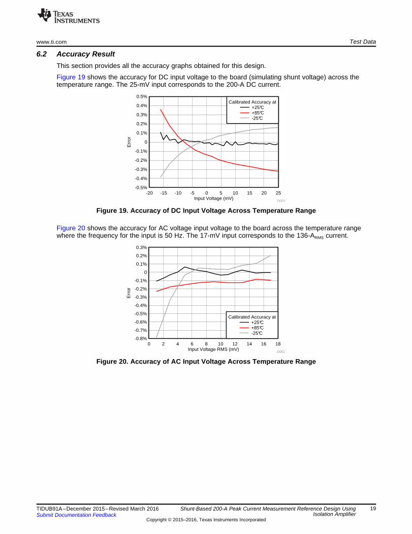
6.2 Accuracy ResultThis section provides all the accuracy graphs obtained for this design.
Figure 19 shows the accuracy for DC input voltage to the board (simulating shunt voltage) across thetemperature range. The 25-mV input corresponds to the 200-A DC current.
Figure 19. Accuracy of DC Input Voltage Across Temperature Range
Figure 20 shows the accuracy for AC voltage input voltage to the board across the temperature rangewhere the frequency for the input is 50 Hz. The 17-mV input corresponds to the 136-ARMS current.
Figure 20. Accuracy of AC Input Voltage Across Temperature Range

Input Current RMS (A)
Err
or
5 10 15 20 25 30 35 40 45 50 55 60-1.75%
-1.5%
-1.25%
-1%
-0.75%
-0.5%
-0.25%
0
0.25%
0.5%
0.75%
D006
Uncalibrated Accuracy ofFront Gain StageAMCLevel ShifterOverall System
Input Voltage (mV)
Err
or
-20 -15 -10 -5 0 5 10 15 20 25-2.5%
-2%
-1.5%
-1%
-0.5%
0
0.5%
1%
1.5%
2%
D004
Uncalibrated Accuracy ofFront Gain StageAMCLevel ShifterOverall System
Input Voltage (mV)
Err
or
0 2 4 6 8 10 12 14 16 18-1.5%
-1.25%
-1%
-0.75%
-0.5%
-0.25%
0
0.25%
D005
Uncalibrated Accuracy ofFront Gain StageAMCLevel ShifterOverall System
Input Current RMS (A)
Err
or
10 15 20 25 30 35 40 45 50 55 60-0.4%
-0.3%
-0.2%
-0.1%
0
0.1%
0.2%
0.3%
0.4%
D003
Calibrated Accuracy at+25°C+85°C-25°C
Test Data www.ti.com
20 TIDUB91A–December 2015–Revised March 2016Submit Documentation Feedback
Copyright © 2015–2016, Texas Instruments Incorporated
Shunt-Based 200-A Peak Current Measurement Reference Design UsingIsolation Amplifier
Figure 21 shows the accuracy for AC current input wherein the current was passed through the shuntresistor of 125 μΩ and the voltage drop across shunt was fed to the board as an input voltage.
Figure 21. Accuracy of AC Current Input Across Temperature Range
The following figures provide a deeper analysis wherein the behavior of all the stages is shown separatelyfor various tests conducted at 25°C. Figure 22 shows the behavior of the individual stages for the DC inputvoltage. Figure 23 and Figure 24 show the behavior for AC voltage input and AC current input flowingthrough the shunt, respectively.
Figure 22. Accuracy of System at 25°C (DC InputVoltage)
Figure 23. Accuracy of System at 25°C (ACRMS InputVoltage)
Figure 24. Accuracy of System at 25°C (AC Current Input)

Output of AMC
Input to AMC
www.ti.com Test Data
21TIDUB91A–December 2015–Revised March 2016Submit Documentation Feedback
Copyright © 2015–2016, Texas Instruments Incorporated
Shunt-Based 200-A Peak Current Measurement Reference Design UsingIsolation Amplifier
6.3 Time ResponseThis section shows the response of the design to a step input of 25 mV. Figure 25 shows the total risetime of the input and corresponding rise time of the output.
Figure 25. Rise Time of Input (CH1) and Output (CH2)
The measured rise time of the step input is 16.76 μs and the corresponding rise time of output is 29 μs.Figure 26 shows the rise time of only the AMC1200 when a step input of 250 mV is fed to it.
Figure 26. Rise Time of AMC1200

Output
Step input
Output of AMC
Input to AMC
Test Data www.ti.com
22 TIDUB91A–December 2015–Revised March 2016Submit Documentation Feedback
Copyright © 2015–2016, Texas Instruments Incorporated
Shunt-Based 200-A Peak Current Measurement Reference Design UsingIsolation Amplifier
The rise time of the input to the AMC1200 is 19.90 μs, and the corresponding rise time of the AMC1200 is21.36 μs. Figure 27 and Figure 28 show the propagation delay of the AMC1200 and the entire board,respectively.
Figure 27. Propagation Delay of AMC1200
Figure 28. Propagation Delay of the Board
As seen in these waveforms, the measured propagation delay of the AMC1200 is 2.4 μs and the boardis 7 μs.

5.10k
R8
1.27kR9
6.34k
R7
GND2
V3.3
V3.3
GND2
VBIAS1
GND2
EN3
VIN4
VREF5
U6
REF2033AIDDCR
V3.3
V1.65
GND2
P5V
V1.65
GND2
GND2
P5V
61
3
5
4
2
T1
750342879
VCC
VEE
VEE
VCC
GND1
GND1
GND1
GND1
GND2
GND2
GND2
1
2
J2
1725656
0.1µF
C12
0.1µF
C6
0.1µF
C4
0.1µF
C7
0.1µF
C9
0.1µF
C8
0.1µF
C15
P5V
GND2
GND2
0.1µFC10
VINP
VINN
VINP
VINN
D11
VCC2
D23
GND4
GND5
U5
SN6501DBVR
GND2
0.1µF
C11
GND2
0R3
GND1
0.1µFC16
GND2
GND1
VEE
1: 3.5
D4
MBR0520LT1G
GND2
1
2345
J3142-0701-201
TP3
TP4
TP7
TP5
TP9
TP10
TP13
TP8
TP11
TP6
TP12
VCC
TP1
TP2
Green
12
D1
Green
12
D5
1.00kR15
10µFC13
10µFC5
D3
MBR0540T1G
D2
MBR0540T1G
1µFC1
1µFC2
NC
U2
LM4040BIM3-2.5
NC
U1
LM4040BIM3-2.5
576R6
576R5
1
2
J1
1725656
10µFC14
0.22µFC3
18
R1
18
R20.22µFC17
36
R14
1.00kR4
20.0k
R11
20.0kR10
14.7k
R13
14.7kR12
1
2
3
4
5
6
7
8
+
-
V+
V-
V-
V+
U4
AMC1200BDWV
12.0
R16
12.0
R17 330pF C18
12.0
R18
12.0
R19
330pFC19
1
3
2
48
U3A
OPA2376AID
7
5
6
48
U3BOPA2376AID
1
2
3
4
5
U7OPA376AIDBVR
www.ti.com Design Files
23TIDUB91A–December 2015–Revised March 2016Submit Documentation Feedback
Copyright © 2015–2016, Texas Instruments Incorporated
Shunt-Based 200-A Peak Current Measurement Reference Design UsingIsolation Amplifier
7 Design Files
7.1 SchematicsTo download the schematics, see the design files at TIDA-00445.
Figure 29. TIDA-00445 Schematic

Design Files www.ti.com
24 TIDUB91A–December 2015–Revised March 2016Submit Documentation Feedback
Copyright © 2015–2016, Texas Instruments Incorporated
Shunt-Based 200-A Peak Current Measurement Reference Design UsingIsolation Amplifier
7.2 Bill of MaterialsTo download the bill of materials (BOM), see the design files at TIDA-00445.
7.3 PCB Layout Recommendations• No copper between isolation with a minimum width of 9 mm (as represented by the arrows in
Figure 30).
Figure 30. PCB Layout Showing Isolation Between High- and Low-Voltage Side of AMC1200
• Do not place any test points near the transformer to avoid noise pick up.• Place decoupling capacitors very close to their corresponding pins with a low impedance path to the
device GND.

www.ti.com Design Files
25TIDUB91A–December 2015–Revised March 2016Submit Documentation Feedback
Copyright © 2015–2016, Texas Instruments Incorporated
Shunt-Based 200-A Peak Current Measurement Reference Design UsingIsolation Amplifier
Figure 31. PCB Layout Representing Signal Chain
• Keep trace length from the input to signal chain equal and make sure the entire signal chain is in onestraight line (as represented in Figure 31).
• Place input resistors very close to their corresponding pins. Traces for output resistors can be a littlelonger if required.
• Make sure to have non-plated mounting if any are between isolated regions.
7.3.1 Layout PrintsTo download the layout prints, see the design files at TIDA-00445.
7.4 Altium ProjectTo download the Altium project files, see the design files at TIDA-00445.
7.5 Gerber FilesTo download the Gerber files, see the design files at TIDA-00445.
7.6 Assembly DrawingsTo download the assembly drawings, see the design files at TIDA-00445.

About the Authors www.ti.com
26 TIDUB91A–December 2015–Revised March 2016Submit Documentation Feedback
Copyright © 2015–2016, Texas Instruments Incorporated
Shunt-Based 200-A Peak Current Measurement Reference Design UsingIsolation Amplifier
8 About the AuthorsN. NAVANEETH KUMAR is a Systems Architect at Texas Instruments, where he is responsible fordeveloping subsystem solutions for motor controls within Industrial Systems. N. Navaneeth brings to thisrole his extensive experience in power electronics, EMC, analog, and mixed signal designs. He hassystem-level product design experience in drives, solar inverters, UPS, and protection relays. N.Navaneeth earned his bachelor of electronics and communication engineering from Bharathiar University,India and his master of science in electronic product development from Bolton University, UK.
NEHA NAIN is a Systems Engineer at Texas Instruments, where she is responsible for developingsubsystem reference design solutions for Industrial equipment. Neha earned her bachelor of electrical andelectronics engineering from PES Institute of Technology (now PES University), Bangalore.

www.ti.com Revision History
27TIDUB91A–December 2015–Revised March 2016Submit Documentation Feedback
Copyright © 2015–2016, Texas Instruments Incorporated
Revision History
Revision HistoryNOTE: Page numbers for previous revisions may differ from page numbers in the current version.
Changes from Original (December 2015) to A Revision ................................................................................................ Page
• Changed from preview page............................................................................................................. 1

IMPORTANT NOTICE FOR TI REFERENCE DESIGNS
Texas Instruments Incorporated ("TI") reference designs are solely intended to assist designers (“Buyers”) who are developing systems thatincorporate TI semiconductor products (also referred to herein as “components”). Buyer understands and agrees that Buyer remainsresponsible for using its independent analysis, evaluation and judgment in designing Buyer’s systems and products.TI reference designs have been created using standard laboratory conditions and engineering practices. TI has not conducted anytesting other than that specifically described in the published documentation for a particular reference design. TI may makecorrections, enhancements, improvements and other changes to its reference designs.Buyers are authorized to use TI reference designs with the TI component(s) identified in each particular reference design and to modify thereference design in the development of their end products. HOWEVER, NO OTHER LICENSE, EXPRESS OR IMPLIED, BY ESTOPPELOR OTHERWISE TO ANY OTHER TI INTELLECTUAL PROPERTY RIGHT, AND NO LICENSE TO ANY THIRD PARTY TECHNOLOGYOR INTELLECTUAL PROPERTY RIGHT, IS GRANTED HEREIN, including but not limited to any patent right, copyright, mask work right,or other intellectual property right relating to any combination, machine, or process in which TI components or services are used.Information published by TI regarding third-party products or services does not constitute a license to use such products or services, or awarranty or endorsement thereof. Use of such information may require a license from a third party under the patents or other intellectualproperty of the third party, or a license from TI under the patents or other intellectual property of TI.TI REFERENCE DESIGNS ARE PROVIDED "AS IS". TI MAKES NO WARRANTIES OR REPRESENTATIONS WITH REGARD TO THEREFERENCE DESIGNS OR USE OF THE REFERENCE DESIGNS, EXPRESS, IMPLIED OR STATUTORY, INCLUDING ACCURACY ORCOMPLETENESS. TI DISCLAIMS ANY WARRANTY OF TITLE AND ANY IMPLIED WARRANTIES OF MERCHANTABILITY, FITNESSFOR A PARTICULAR PURPOSE, QUIET ENJOYMENT, QUIET POSSESSION, AND NON-INFRINGEMENT OF ANY THIRD PARTYINTELLECTUAL PROPERTY RIGHTS WITH REGARD TO TI REFERENCE DESIGNS OR USE THEREOF. TI SHALL NOT BE LIABLEFOR AND SHALL NOT DEFEND OR INDEMNIFY BUYERS AGAINST ANY THIRD PARTY INFRINGEMENT CLAIM THAT RELATES TOOR IS BASED ON A COMBINATION OF COMPONENTS PROVIDED IN A TI REFERENCE DESIGN. IN NO EVENT SHALL TI BELIABLE FOR ANY ACTUAL, SPECIAL, INCIDENTAL, CONSEQUENTIAL OR INDIRECT DAMAGES, HOWEVER CAUSED, ON ANYTHEORY OF LIABILITY AND WHETHER OR NOT TI HAS BEEN ADVISED OF THE POSSIBILITY OF SUCH DAMAGES, ARISING INANY WAY OUT OF TI REFERENCE DESIGNS OR BUYER’S USE OF TI REFERENCE DESIGNS.TI reserves the right to make corrections, enhancements, improvements and other changes to its semiconductor products and services perJESD46, latest issue, and to discontinue any product or service per JESD48, latest issue. Buyers should obtain the latest relevantinformation before placing orders and should verify that such information is current and complete. All semiconductor products are soldsubject to TI’s terms and conditions of sale supplied at the time of order acknowledgment.TI warrants performance of its components to the specifications applicable at the time of sale, in accordance with the warranty in TI’s termsand conditions of sale of semiconductor products. Testing and other quality control techniques for TI components are used to the extent TIdeems necessary to support this warranty. Except where mandated by applicable law, testing of all parameters of each component is notnecessarily performed.TI assumes no liability for applications assistance or the design of Buyers’ products. Buyers are responsible for their products andapplications using TI components. To minimize the risks associated with Buyers’ products and applications, Buyers should provideadequate design and operating safeguards.Reproduction of significant portions of TI information in TI data books, data sheets or reference designs is permissible only if reproduction iswithout alteration and is accompanied by all associated warranties, conditions, limitations, and notices. TI is not responsible or liable forsuch altered documentation. Information of third parties may be subject to additional restrictions.Buyer acknowledges and agrees that it is solely responsible for compliance with all legal, regulatory and safety-related requirementsconcerning its products, and any use of TI components in its applications, notwithstanding any applications-related information or supportthat may be provided by TI. Buyer represents and agrees that it has all the necessary expertise to create and implement safeguards thatanticipate dangerous failures, monitor failures and their consequences, lessen the likelihood of dangerous failures and take appropriateremedial actions. Buyer will fully indemnify TI and its representatives against any damages arising out of the use of any TI components inBuyer’s safety-critical applications.In some cases, TI components may be promoted specifically to facilitate safety-related applications. With such components, TI’s goal is tohelp enable customers to design and create their own end-product solutions that meet applicable functional safety standards andrequirements. Nonetheless, such components are subject to these terms.No TI components are authorized for use in FDA Class III (or similar life-critical medical equipment) unless authorized officers of the partieshave executed an agreement specifically governing such use.Only those TI components that TI has specifically designated as military grade or “enhanced plastic” are designed and intended for use inmilitary/aerospace applications or environments. Buyer acknowledges and agrees that any military or aerospace use of TI components thathave not been so designated is solely at Buyer's risk, and Buyer is solely responsible for compliance with all legal and regulatoryrequirements in connection with such use.TI has specifically designated certain components as meeting ISO/TS16949 requirements, mainly for automotive use. In any case of use ofnon-designated products, TI will not be responsible for any failure to meet ISO/TS16949.IMPORTANT NOTICE
Mailing Address: Texas Instruments, Post Office Box 655303, Dallas, Texas 75265Copyright © 2016, Texas Instruments Incorporated