21.3: Adappqtive Equalization and Data Recovery in a Dual ...
33
21.3: Adaptive Equalization and Data Recovery in a Dual-Mode (PAM2/4) Serial Link Transceiver Vladimir Stojanovic 1,2 , Andrew Ho 1 , Bruno Garlepp 1 , 1 1 12 1 Fred Chen 1 , Jason Wei 1 , Elad Alon 1,2 , Carl Werner 1 , Jared Zerbe 1 and Mark Horowitz 2 1 Rambus Inc 1 Rambus Inc. 2 Stanford University
Transcript of 21.3: Adappqtive Equalization and Data Recovery in a Dual ...
21.3: Adaptive Equalization and Data p qRecovery in a Dual-Mode (PAM2/4)
Serial Link Transceiver
Vladimir Stojanovic1,2, Andrew Ho1, Bruno Garlepp1, 1 1 1 2 1Fred Chen1, Jason Wei1, Elad Alon1,2, Carl Werner1,
Jared Zerbe1 and Mark Horowitz2
1 Rambus Inc1 Rambus Inc.2 Stanford University
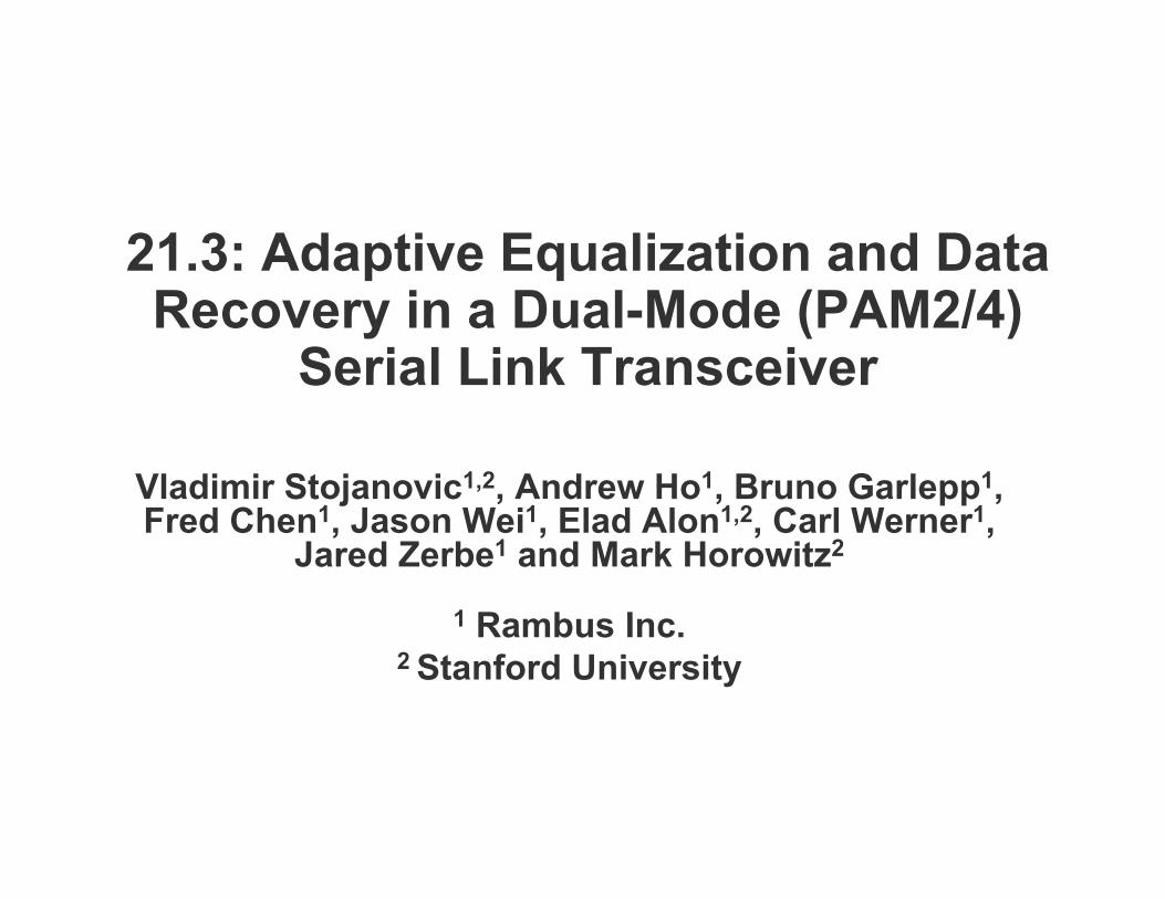
Backplane channels0
dB]
p
• Same backplane
-20
-10
enua
tion
[d 9" FR4Same backplane• Loss is variable
50
-40
-30Atte
9" FR4, i t b
26" FR4• Custom fit• Equalization
-60
-50 via stub
26" FR4,via stub
• Modulation
• Lots of different links 0 2 4 6 8 10frequency [GHz]
• Lots of different links• Huge control overhead• Nice to have link adapt itself to the channelNice to have link adapt itself to the channel
• Adapt both coefficients and modulation/equalization type
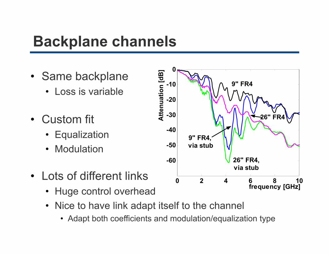
Backplane channel – variable in timep
dB• Changes in time• Temperature
H idit
dB
• Humidity
• Slow but significant• Need to re-adjust the
equalizerCan do with slow• Can do with slow, simple hardware
GHz
G. Sheets, J. D’Ambrosia “The Impact of Environmental Conditions on Channel Performance," DesignCon 2004
Outline• Show adaptive and reconfigurable link
• Minimum hardware overhead
• Link equalization and modulation• Dual-mode (PAM2/PAM4) linkDual mode (PAM2/PAM4) link• Making the link adaptive
Results• Results
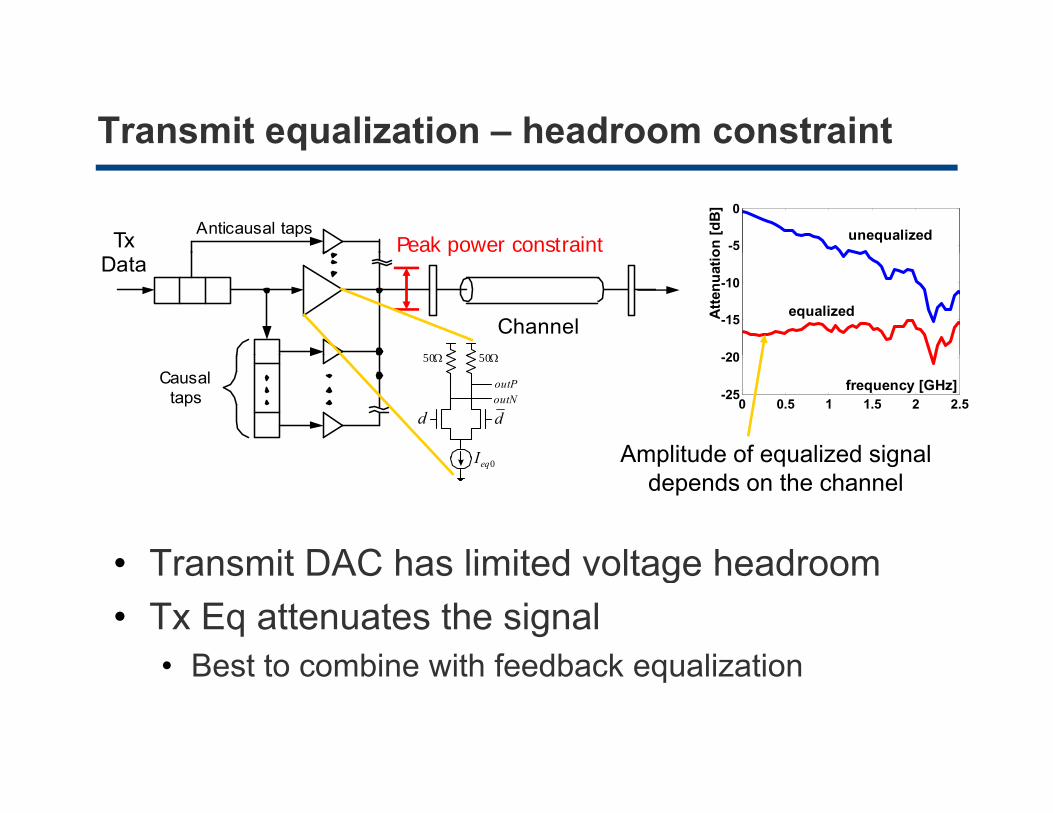
Transmit equalization – headroom constraintq
-5
0
on [d
B]
unequalizedTx Anticausal tapsPeak power constraint
20
-15
-10
Atte
nuat
io
equalized
Data
Channel
p
Ω50Ω50
0 0.5 1 1.5 2 2.5-25
-20
frequency [GHz]
Amplitude of equalized signal
Causaltaps
I
doutNoutP
d
Ω50Ω50
• Transmit DAC has limited voltage headroom
Amplitude of equalized signaldepends on the channel
0eqI
• Transmit DAC has limited voltage headroom• Tx Eq attenuates the signal
• Best to combine with feedback equalization• Best to combine with feedback equalization
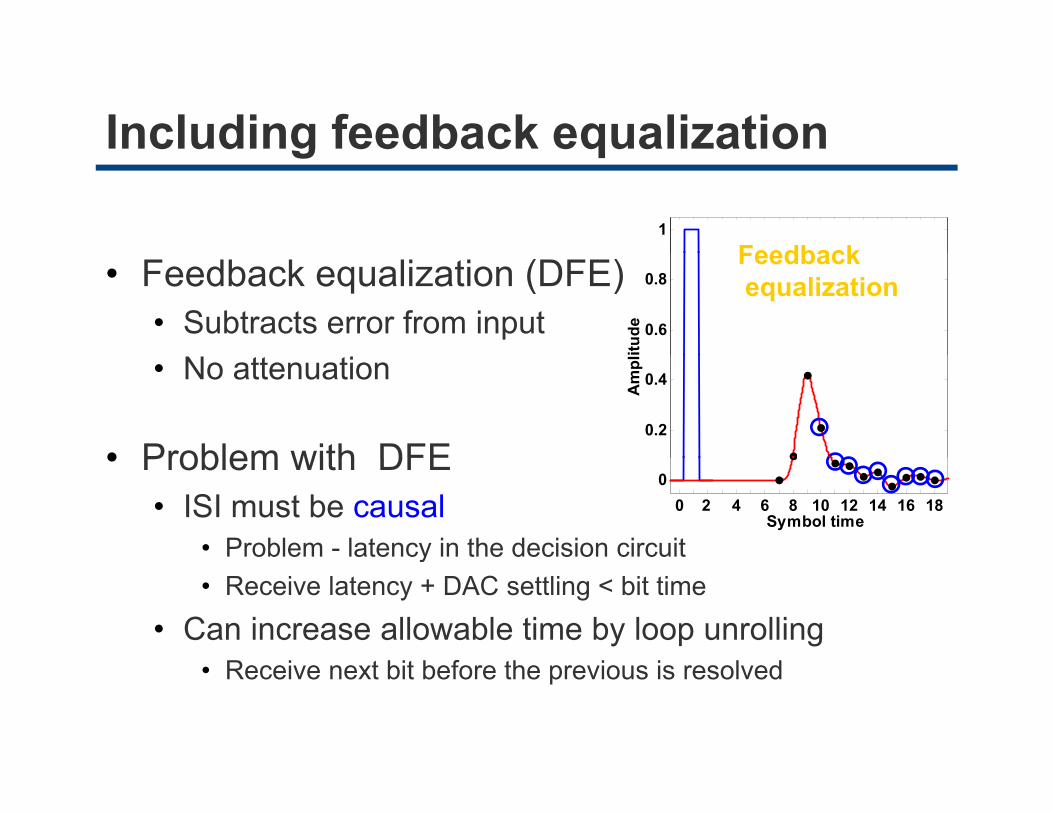
Including feedback equalizationg q
1
Feedback• Feedback equalization (DFE)• Subtracts error from input 0.6
0.8
itude
Feedbackequalization
• No attenuation
• Problem with DFE0.2
0.4Am
pl
• Problem with DFE• ISI must be causal
• Problem - latency in the decision circuit
0 2 4 6 8 10 12 14 16 180
Symbol time
y• Receive latency + DAC settling < bit time
• Can increase allowable time by loop unrollingR i t bit b f th i i l d• Receive next bit before the previous is resolved
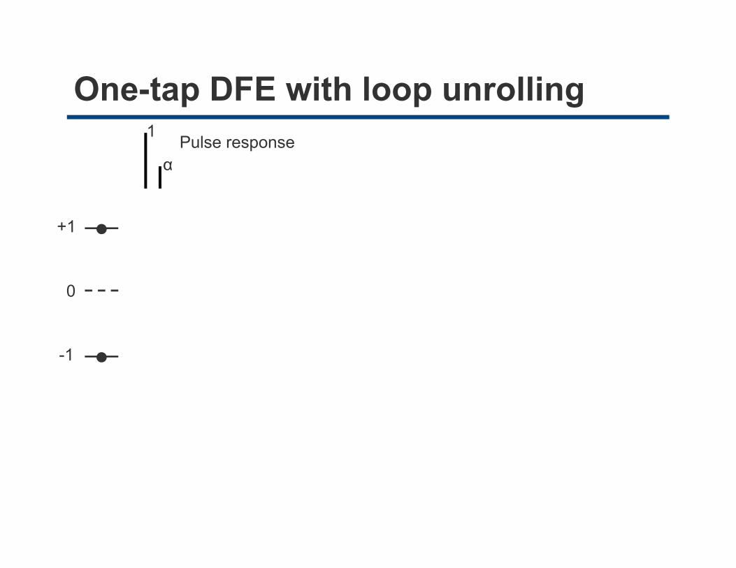
One-tap DFE with loop unrollingp p g1
αPulse response
+1
0
-1
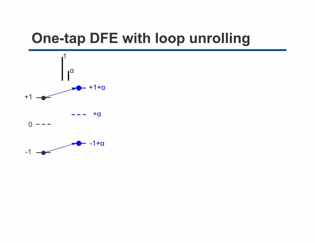
One-tap DFE with loop unrollingp p g1
α
+1+1+α
0+α
-1-1+α
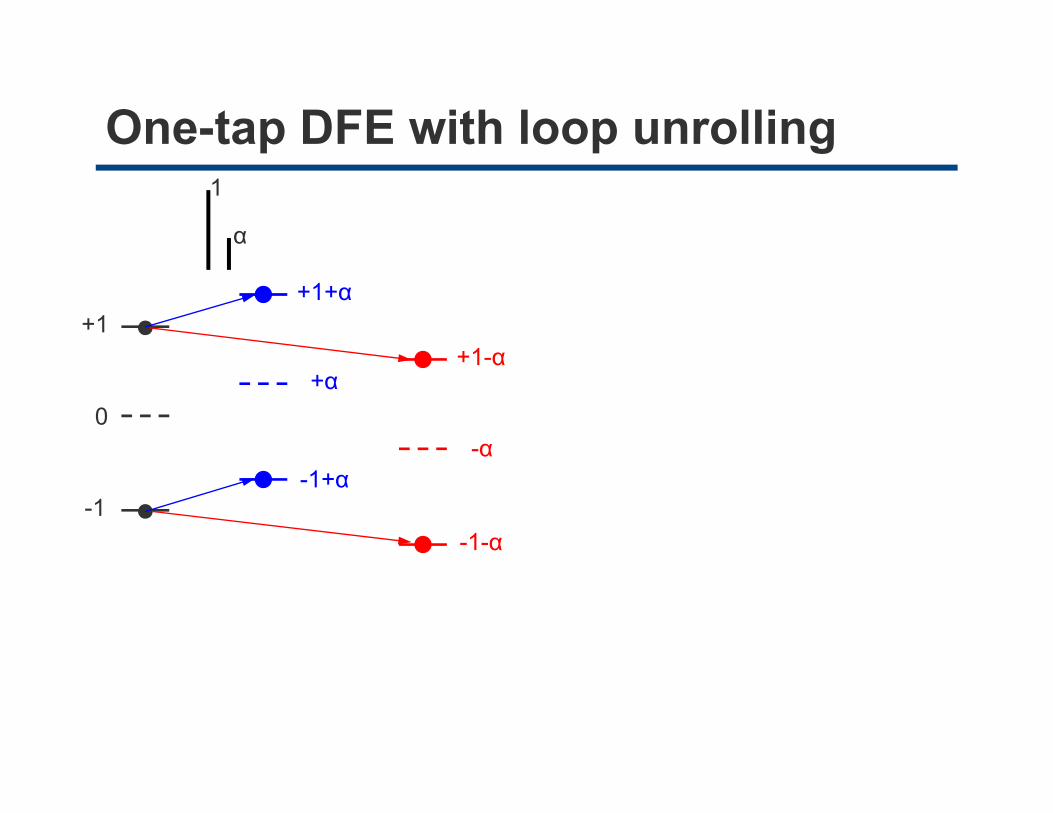
One-tap DFE with loop unrollingp p g1
α
+1+1+α
+1 α
0+α
+1-α
-α
-1-1+α
-1-α
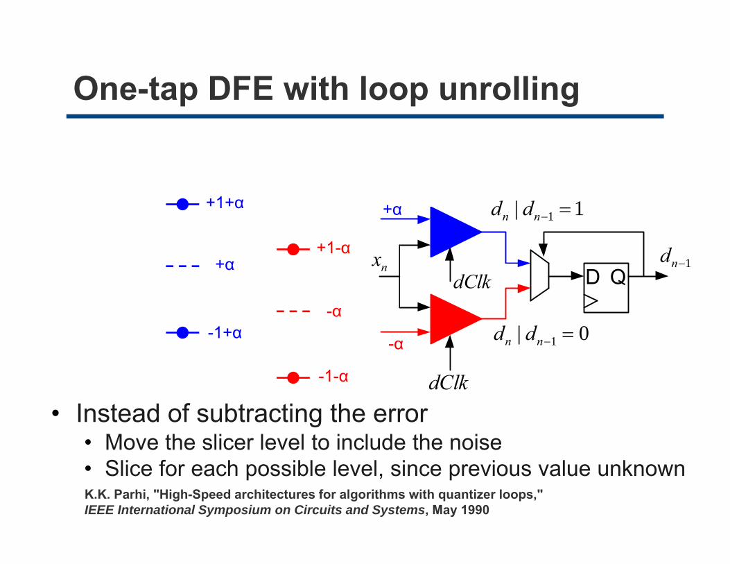
One-tap DFE with loop unrollingp p g
+1+α
+1 α
1| 1 =−nn dd+α
+α+1-α
-α
D Q1−nd
dClknx
-1+α
-1-α dClk
0| 1 =−nn dd-α
• Instead of subtracting the error• Move the slicer level to include the noise
S f
dClk
• Slice for each possible level, since previous value unknownK.K. Parhi, "High-Speed architectures for algorithms with quantizer loops," IEEE International Symposium on Circuits and Systems, May 1990
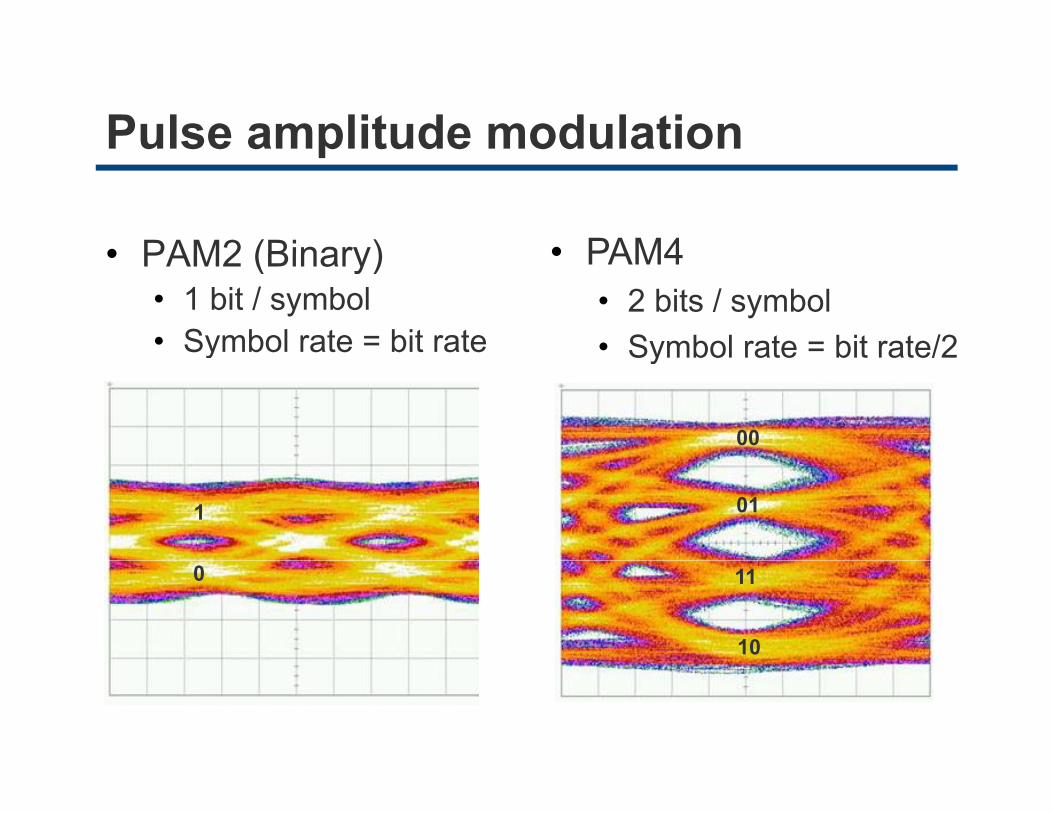
Pulse amplitude modulationp
• PAM2 (Binary) • PAM4• PAM2 (Binary)• 1 bit / symbol• Symbol rate = bit rate
• PAM4 • 2 bits / symbol• Symbol rate = bit rate/2y Symbol rate bit rate/2
00
011
10
110
Outline• Show adaptive and reconfigurable link
• Minimum hardware overhead
• Link equalization and modulation• Dual-mode (PAM2/PAM4) linkDual mode (PAM2/PAM4) link• Making the link adaptive
Results• Results
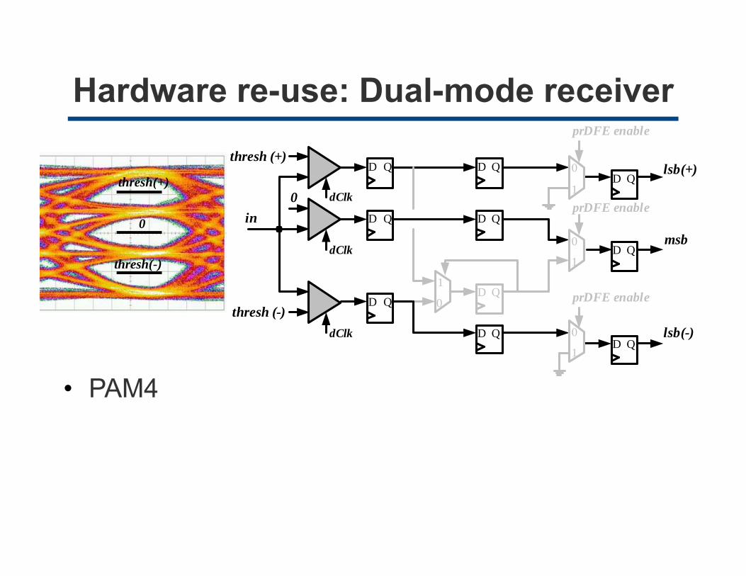
Hardware re-use: Dual-mode receiver
D QD Qthresh (+)
lsb(+)
prDFE enable
D Q0
th h(+)
D Q D Qin0
msb
prDFE enabledClk
dClk
D Q
D Q0
1thresh(+)
0
D Qthresh (-)
dClk
prDFE enable
D Q
D Q1
0
1thresh(-)
• PAM4
lsb(-)D QdClkD Q
0
1
PAM4
Hardware re-use: Dual-mode receiver
D QD Qthresh (+)
lsb(+)
prDFE enable
D Q0
th h(+)
D Q D Qin0
msb
prDFE enabledClk
dClk
D Q
D Q0
1thresh(+)
0
D Qthresh (-)
dClk
prDFE enable
D Q
D Q1
0
1
outN
clkclk
Q
thresh(-)
lsb(-)D QdClkD Q
0
1inP
inNinP
outNoutP
outP outN
Q
• PAM4 inNclkthreshII
+2 threshII
−2 Q
PAM4
pre-amp with offset comparator
Hardware re-use: Dual-mode receiver
D QD Qthresh (+)
lsb(+)
prDFE enable
D Q0
0 D Q D Qin0
msb
prDFE enabledClk
dClk
D Q
D Q0
1
D Qthresh (-)
dClk
prDFE enable
D Q
D Q1
0
1
lsb(-)D QdClkD Q
0
1
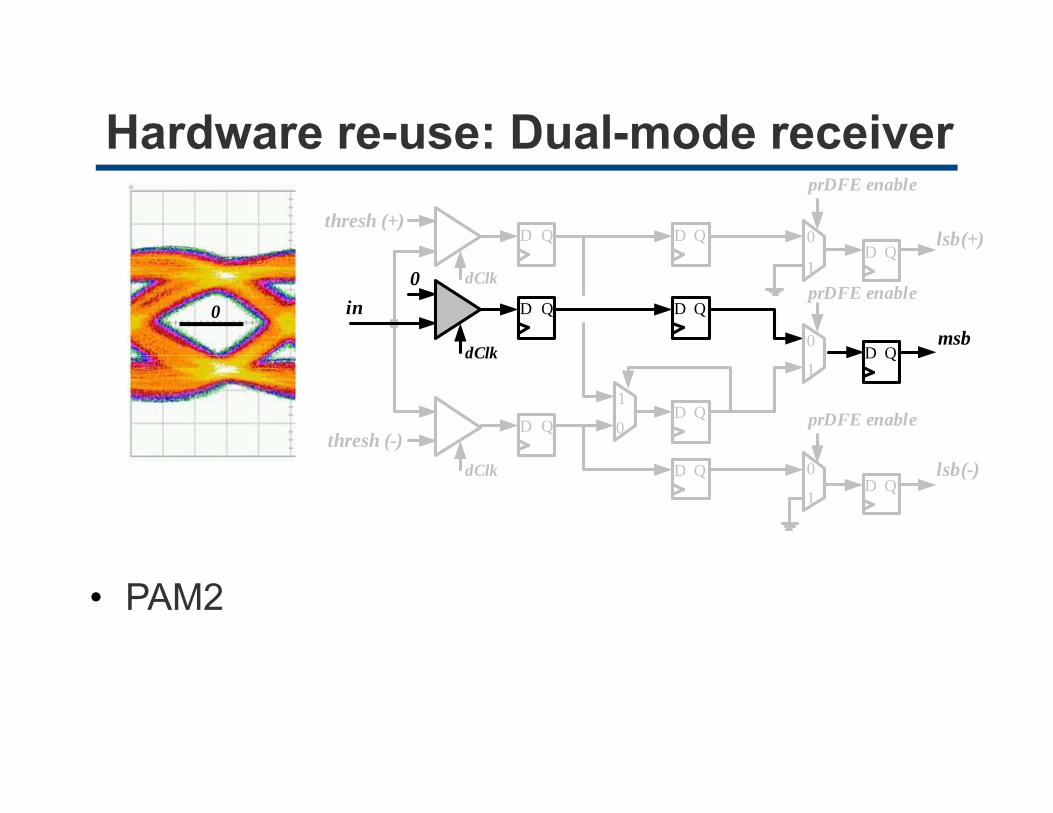
• PAM2
Hardware re-use: Dual-mode receiver
D QD Qthresh (+)
lsb(+)
prDFE enable
D Q0
D Q D Qin0
msb
prDFE enabledClk
dClk
D Q
D Q0
1
D Qthresh (-)
dClk
prDFE enable
D Q
D Q1
0
1
lsb(-)D QdClkD Q
0
1
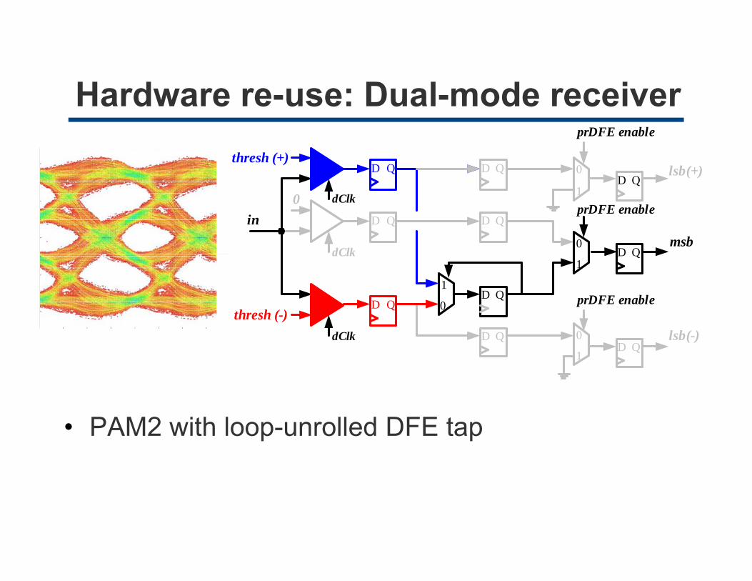
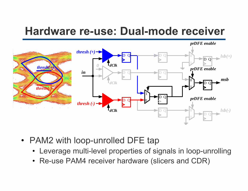
• PAM2 with loop-unrolled DFE tap
Hardware re-use: Dual-mode receiver
D QD Qthresh (+)
lsb(+)
prDFE enable
D Q0
thresh(+)D Q D Qin
0
msb
prDFE enabledClk
dClk
D Q
D Q0
1
thresh(-)
D Qthresh (-)
dClk
prDFE enable
D Q
D Q1
0
1
lsb(-)D QdClkD Q
0
1
• PAM2 with loop-unrolled DFE tap• Leverage multi-level properties of signals in loop-unrolling• Re-use PAM4 receiver hardware (slicers and CDR)
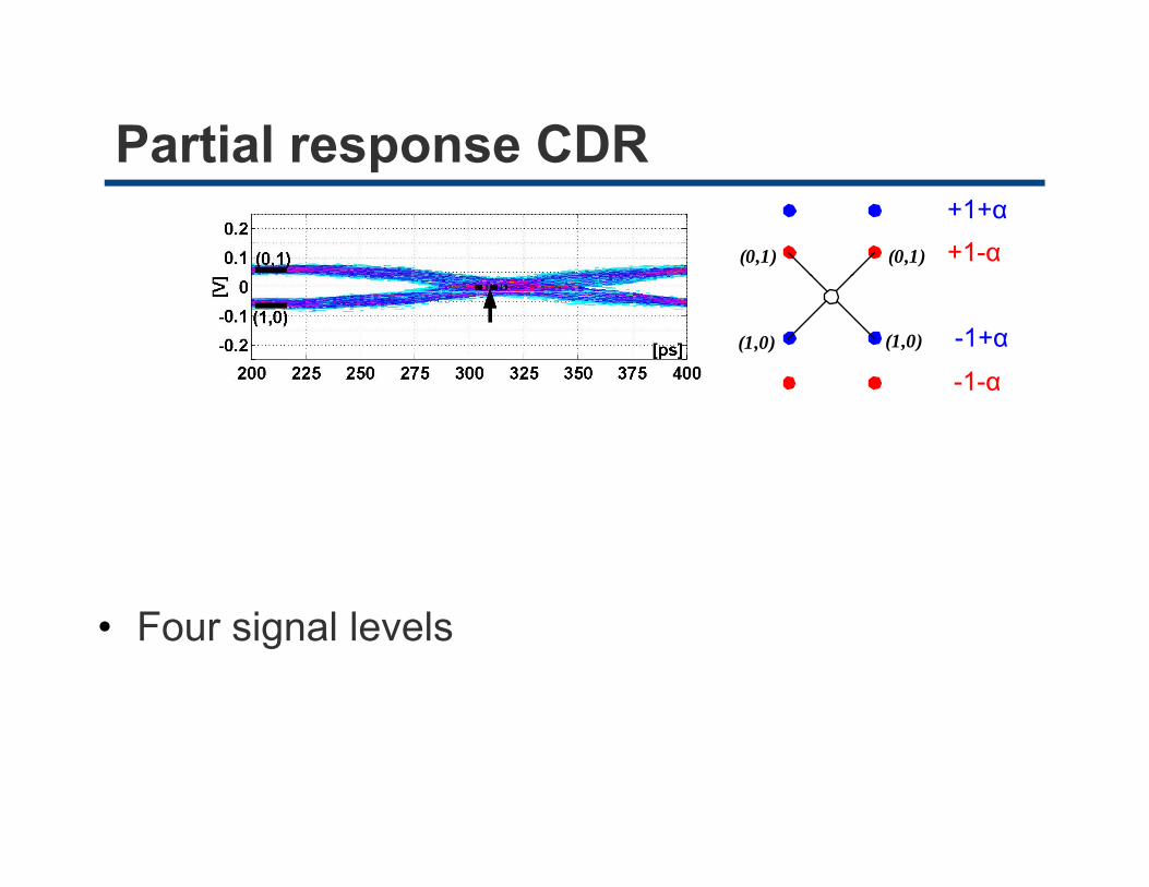
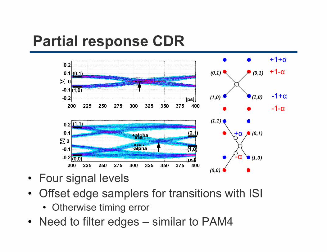
Partial response CDRp+1+α+1-α(0,1) (0,1)
-1-α
-1+α(1,0) (1,0)
1 α
F i l l l• Four signal levels
Partial response CDRp+1+α+1-α(0,1) (0,1)
-1-α
-1+α(1,0) (1,0)
1 α(1,1)
(0,1)+α
F i l l l(0,0)
(1,0)-α
• Four signal levels • Offset edge samplers for transitions with ISI
Otherwise timing error• Otherwise timing error• Need to filter edges – similar to PAM4
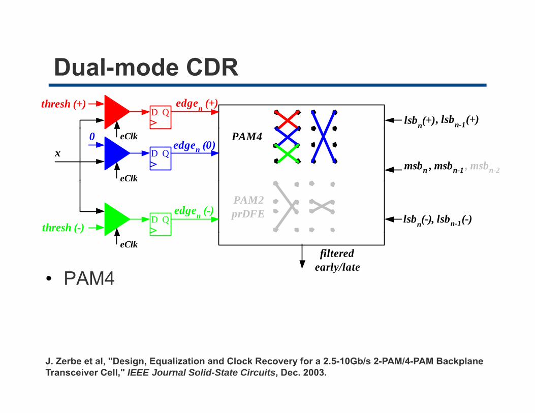
Dual-mode CDRD Q
thresh (+) edgen (+)lsbn(+), lsbn-1(+)
D Qx0 eClk
eClk
edgen (0)PAM4
msbn , msbn-1 , msbn-2
D Qthresh (-)
eClk
edgen (-)PAM2prDFE lsbn(-), lsbn-1(-)
• PAM4
( )eClk
filteredearly/late
PAM4
J. Zerbe et al, "Design, Equalization and Clock Recovery for a 2.5-10Gb/s 2-PAM/4-PAM Backplane Transceiver Cell," IEEE Journal Solid-State Circuits, Dec. 2003.
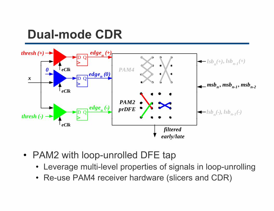
Dual-mode CDRD Q
thresh (+) edgen (+)lsbn(+), lsbn-1(+)
D Qx0 eClk
eClk
edgen (0)PAM4
msbn , msbn-1 , msbn-2
D Qthresh (-)
eClk
edgen (-)PAM2prDFE lsbn(-), lsbn-1(-)
( )eClk
filteredearly/late
• PAM2 with loop-unrolled DFE tap• Leverage multi-level properties of signals in loop-unrolling• Re-use PAM4 receiver hardware (slicers and CDR)
Outline• Show adaptive and reconfigurable link
• Minimum hardware overhead
• Link equalization and modulation• Dual-mode (PAM2/PAM4) linkDual mode (PAM2/PAM4) link• Making the link adaptive
Results• Results
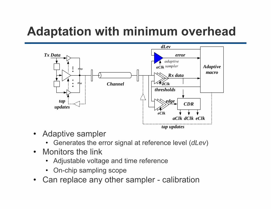
Adaptation with minimum overheadTx Data
dLev
adaptivel
error
Ad i
Channel
sampler
Rx data
Adaptivemacro
thresholds
aClk
dClk
tapupdates CDRedge
aClk dClk eClkeClk
• Adaptive sampler • Generates the error signal at reference level (dLev)
tap updates
aClk dClk eClk
Generates the error signal at reference level (dLev)• Monitors the link
• Adjustable voltage and time reference• On chip sampling scope• On-chip sampling scope
• Can replace any other sampler - calibration
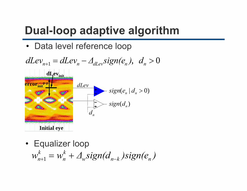
Dual-loop adaptive algorithmp p g• Data level reference loop
0>d)sign(eΔdLevdLevdLevinitdLevinitdLevinit
error p-p dL
0,1 >−=+ nndLevnn d)sign(eΔdLevdLev
errorinitp p
)0|( >nn designdLev
)( ndsign
Initial eyeInitial eye
nd
• Equalizer loop))sign(esign(dΔww kk += ))sign(esign(dΔww nknwnn −+ +=1
Dual-loop adaptive algorithmp p g• Data level reference loop
0>d)sign(eΔdLevdLevdLevinit dLevmid dLev
dLevinit dLevmid dLev
dLevinit dLevmid dLeverror p-p
0,1 >−=+ nndLevnn d)sign(eΔdLevdLev
… …
dLevend
… …
dLevend
… …
dLevenderrorinitp p
dLev
Initial eye Mid-way equalized EqualizedInitial eye Mid-way equalized Equalizednd
• Equalizer loop))sign(esign(dΔww kk +=
• Scale the equalizer - output Tx constraint
))sign(esign(dΔww nknwnn −+ +=1
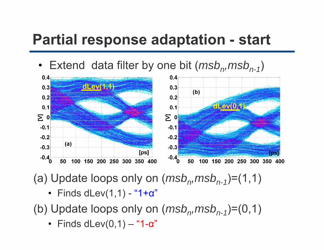
Partial response adaptation - startp p• Extend data filter by one bit (msbn,msbn-1)
(a) Update loops only on (msbn,msbn-1)=(1,1)• Finds dLev(1,1) - “1+α”
(b) Update loops only on (msbn,msbn-1)=(0,1)• Finds dLev(0,1) – “1-α”
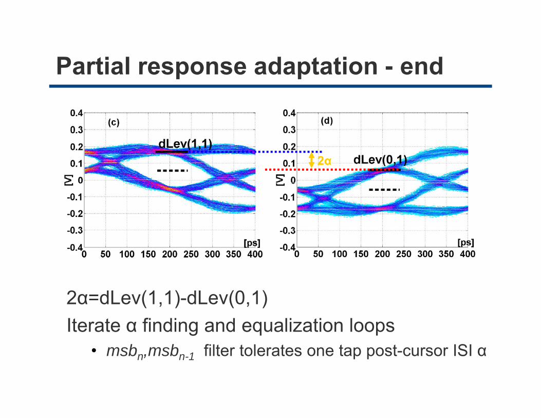
Partial response adaptation - endp p
2α
2α=dLev(1,1)-dLev(0,1)Iterate α finding and equalization loops
• msbn,msbn-1 filter tolerates one tap post-cursor ISI α
Outline• Show adaptive and reconfigurable link
• Minimum hardware overhead
• Link equalization and modulation• Dual-mode (PAM2/PAM4) linkDual mode (PAM2/PAM4) link• Making the link adaptive
Results• Results
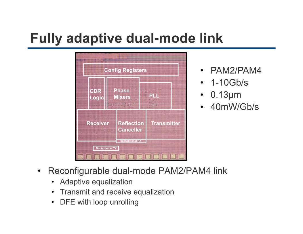
Fully adaptive dual-mode linky p
• PAM2/PAM4Config Registers PAM2/PAM4• 1-10Gb/s• 0.13µm
g g
PhaseMixers
CDRLogic PLL
• 40mW/Gb/sTransmitterReflection
CancellerReceiver
Backchannel RX
Backchannel TX
• Reconfigurable dual-mode PAM2/PAM4 link• Adaptive equalization• Transmit and receive equalization• Transmit and receive equalization• DFE with loop unrolling
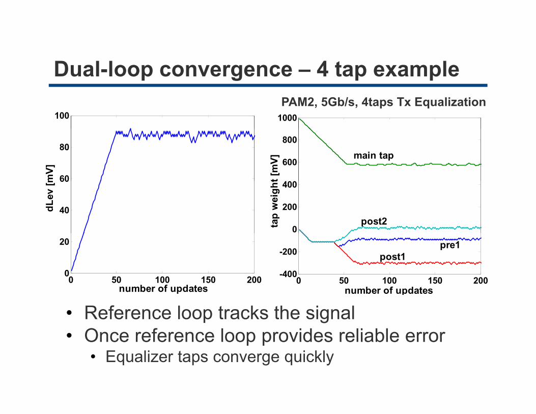
Dual-loop convergence – 4 tap exampleua oop co e ge ce tap e a p e
1000100PAM2, 5Gb/s, 4taps Tx Equalization
600
800
t [m
V] main tap
60
80
mV]
0
200
400
tap
wei
ght
post2 40
60
dLev
[m
0 50 100 150 200-400
-200 post1 pre1
0 50 100 150 2000
20
b f d t
• Reference loop tracks the signal• Once reference loop provides reliable error
number of updatesnumber of updates
Once reference loop provides reliable error• Equalizer taps converge quickly
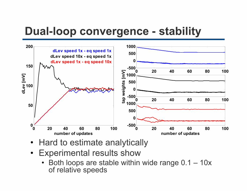
Dual-loop convergence - stabilityp g y200
dLev speed 1x - eq speed 1x dLev speed 10x - eq speed 1x
0500
1000
150
[mV]
dLev speed 1x - eq speed 10x
0 20 40 60 80 100-500
0
ts [m
V]
5001000
50
100
dLev
tap
wei
ght
0 20 40 60 80 100-500
0
1000
0 20 40 60 80 1000
0 20 40 60 80 100-500
0500
• Hard to estimate analytically• Experimental results show
number of updates number of updates
Experimental results show • Both loops are stable within wide range 0.1 – 10x
of relative speeds
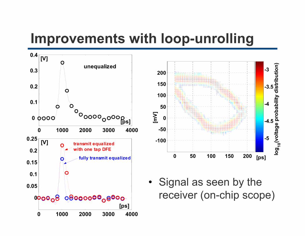
Improvements with loop-unrollingp p g
200 -3 tion)
0.3
0.4 [V] unequalized
100
150
200
4
-3.5
ility
dis
tribu
t
0 1
0.2
-50
0
50
[mV]
-4.5
-4
tage
pro
bab
0 1000 2000 3000 4000
0
0.1
[ps]
0 50 100 150 200
-100
[ps]
-5
log 10
(vol
t
0 15
0.2
0.25 [V] transmit equalized with one tap DFE
fully transmit equalized
• Signal as seen by the i ( hi )
0.05
0.1
0.15
receiver (on-chip scope)0 1000 2000 3000 4000
0[ps]
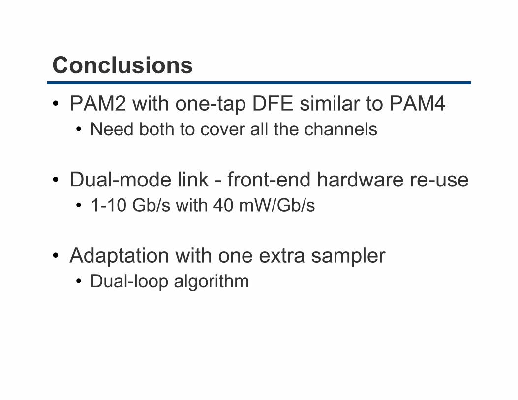
Conclusions• PAM2 with one-tap DFE similar to PAM4
N d b th t ll th h l• Need both to cover all the channels
D l d li k f t d h d• Dual-mode link - front-end hardware re-use• 1-10 Gb/s with 40 mW/Gb/s
• Adaptation with one extra samplerD l l l ith• Dual-loop algorithm