1524.DataSheet.RevD - Renesas Electronics
25
General Description Features ICS1524A Block Diagram Dual Output Phase Controlled SSTL_3/PECL Clock Generator • Wide input frequency range • 8 kHz to 100 MHz • 250 MHz balanced PECL differential outputs • 150 MHz single-ended SSTL_3 clock outputs • Dynamic Phase Adjust (DPA) for DPACLK outputs • Software controlled phase adjustment • 360 o Adjustment down to 1/64 clock increments • External or internal loop filter selection • Uses 3.3 VDC Inputs are 5 volt tolerant. • I 2 C-bus serial interface runs at either low speed (100 kHz) or high speed (400 kHz). • Hardware and Software PLL Lock detection The ICS1524A is a low-cost, very high-performance frequency generator and phase controlled clock synthe- sizer. It is perfectly suited to phase controlled clock synthesis and distribution as well as line-locked and genlocked applications. The ICS1524A offers two channels of clock phase con- trolled outputs; CLK and DPACLK. These two output channels have both 250 MHz PECL differential and 150 MHz SSTL_3 single-ended output pins. The CLK output channel has a fixed phase relationship to the PLL’s input and the DPACLK uses the Dynamic Phase Adjust cir- cuitry to allow control of the clock phase relative to input signal. Optionally, the CLK outputs can operate at half the clock rate and phase aligned with the DPACLK channel, en- abling deMUXing of multiplexed analog-to-digital converters. The FUNC pin provides either the regener- ated input from the phase-locked loop (PLL) divider chain output or a re-synchronized and sharpened input HSYNC. The advanced PLL uses either its internal program- mable feedback divider or an external divider and is programmed by a standard I 2 C-bus™ serial interface. I 2 C-bus is a trademark of Philips Corporation. Applications • Generic Frequency Synthesis • LCD Monitors and Projectors • Genlocking Multiple Video Systems HSYNC OSC IC 2 DPACLK+/- FUNC DPACLK Loop Filter CLK+/- CLK Pin Configuration 24 Pin 300-mil SOIC ICS1524A 1 2 3 4 5 6 7 8 9 10 11 12 24 23 22 21 20 19 18 17 16 15 14 13 VDDD VSSD SDA SCL PDEN EXTFB HSYNC EXTFIL XFILRET VDDA VSSA OSC IREF CLK+ (PECL) C VSSQ VDDQ CLK (SSTL) CLK (SSTL) FUNC (SSTL) LOCK/REF (SSTL) I CADR LK– (PECL) DPACLK+ (PECL) DPACLK– (PECL) DPA 2
Transcript of 1524.DataSheet.RevD - Renesas Electronics
General Description Features
ICS1524A
Block Diagram
Dual Output Phase Controlled SSTL_3/PECL Clock Generator
• Wide input frequency range• 8 kHz to 100 MHz
• 250 MHz balanced PECL differential outputs• 150 MHz single-ended SSTL_3 clock outputs• Dynamic Phase Adjust (DPA) for DPACLK
outputs• Software controlled phase adjustment• 360o Adjustment down to 1/64 clock
increments• External or internal loop filter selection• Uses 3.3 VDC Inputs are 5 volt tolerant.• I2C-bus serial interface runs at either low speed
(100 kHz) or high speed (400 kHz).• Hardware and Software PLL Lock detection
The ICS1524A is a low-cost, very high-performancefrequency generator and phase controlled clock synthe-sizer. It is perfectly suited to phase controlled clocksynthesis and distribution as well as line-locked andgenlocked applications.
The ICS1524A offers two channels of clock phase con-trolled outputs; CLK and DPACLK. These two outputchannels have both 250 MHz PECL differential and 150MHz SSTL_3 single-ended output pins. The CLK outputchannel has a fixed phase relationship to the PLL’s inputand the DPACLK uses the Dynamic Phase Adjust cir-cuitry to allow control of the clock phase relative to inputsignal.
Optionally, the CLK outputs can operate at half the clockrate and phase aligned with the DPACLK channel, en-abling deMUXing of multiplexed analog-to-digitalconverters. The FUNC pin provides either the regener-ated input from the phase-locked loop (PLL) dividerchain output or a re-synchronized and sharpened inputHSYNC.
The advanced PLL uses either its internal program-mable feedback divider or an external divider and isprogrammed by a standard I2C-bus™ serial interface.
I2C-bus is a trademark of Philips Corporation.
Applications• Generic Frequency Synthesis• LCD Monitors and Projectors• Genlocking Multiple Video Systems
HSYNC
OSC
I C2 DPACLK+/-FUNC
DPACLK
LoopFilter
CLK+/-CLK
Pin Configuration
24 Pin 300-mil SOIC
ICS
1524
A
123456789
101112
242322212019181716151413
VDDDVSSD
SDASCL
PDENEXTFBHSYNCEXTFIL
XFILRETVDDAVSSAOSC
IREFCLK+ (PECL)C
VSSQVDDQ
CLK (SSTL)CLK (SSTL)FUNC (SSTL)LOCK/REF (SSTL)I CADR
LK– (PECL)DPACLK+ (PECL)DPACLK– (PECL)
DPA
2
ICS1524A
2
Document Revision HistoryRev A
ICS1523 Rev T Datasheet used as a starting templateNew Block Diagram substituted for old 1523 one
Removed reference to CLK / 2 FunctionalityCreated a set of clock outputs that bypass the DPAExternal PDEN is now the IN-SEL MUX control bit
Text descriptions changed to support new 1524 block diagramRev B
Replaced page 15 “Layout Guidelines”Replaced SIOC Package diagram on page 22“Advanced Status” removedRedrew front page graphics for clairity
Rev CCorrected Chip Revision and Chip Version values on page 5Changed Title on Page 1Minor format changes to pages 8 and 21Corrected pin names on page 10
Rev D Miscellaneous updates to Block Diagram on page 3Changed reference from “Phase Detector” to “Charge Pump”. Pages 4-7, 10
3
ICS1524A
ICS1524A Rev F 05/13/10
PD
EN PD
_Pol
Reg
0x0
:1
PD
EN
Reg
0x0
:0
DPA
CLK
DPA
CLK
+
DPA
CLK
-
CLK CLK
+
CLK
-
PS
DR
eg 0
x1:4
-5P
OS
TS
CA
LER
Div
ider
DPA
_LO
CK
RE
G 1
2:0
PLL
_LO
CK
RE
G 1
2:1
MU
X
Osc
_Div
Reg
0x7
:0-6
Ref_
Pol
Reg
0x0
:2
In_S
elRe
g 0
x7:7
Fbk_
Sel
Reg
0x0
:4Fb
k_Po
lRe
g 0
x0:3
LOC
K/R
EF
EnD
LSRe
g 0
:7
EnPL
SRe
g 0
:6
PFD
Reg
0x1
:0-2
Fill_
Sel
Reg
0x4
:7O
ut_S
clR
eg 0
x6:6
-7
OE
_Tck
Reg
0x6
:1
OE
_Pck
Reg
0x6
:0
OE
_T2
Reg
0x6
:3
OE
_P2
Reg
0x6
:2
OE
_FR
eg 0
x6:4
Ck2
_Inv
Reg
6:5
DPA
_OS
Reg
0x4
:0-5
DPA
_Res
Reg
0x5
:0-1
Func
_Sel
Reg
0x0
:5
FBD
Reg
0x2
:0-7
FBD
Reg
0x3
:0-3
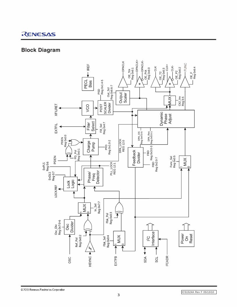
Block Diagram
ICS1524A
4
Pin Descriptions
Notes:1. These LVTTL inputs are 5 V-tolerant.2. Connect to ground if unused.
.ONNIP EMANNIP EPYT NOITPIRCSED STNEMMOC
1 DDDV RWP ylppuslatigiD snoitceslatigidotV3.32 DSSV RWP dnuorglatigiD snoitceslatigidrofdnuorG3 ADS TUO/NI atadlaireS I2 sub-C 1
4 LCS NI kcolclaireS I2 sub-C 1
5 NEDP NI pmuPegrahC pmupegrahcsdnepsuS 1
6 BFTXE NI kcabdeeflanretxE ottupniredividlanretxE DFP 1
7 CNYSH NI cnyslatnoziroH LLPottupnikcolC 1
8 LIFTXE NI retliflanretxE retlifpoolLLPlanretxE9 TERLIFX NI nruterretliflanretxE nruterretlifpoolLLPlanretxE01 ADDV RWP ylppusgolanA yrtiucricgolanarofV3.311 ASSV RWP dnuorggolanA yrtiucricgolanarofdnuorG21 CSO NI rotallicsO rotallicsolatsyrcmorftupnI egakcap 2,1
31 I2 RDAC NI I2 sserddaCIpihC 2 tcelessserddaC
etirwhC4,daerhD4=woLetirwhE4,daerhF4=hgiH
41 FER/KCOL LTSS ecnerefer/rotacidnikcoL tupniFERrokcolAPDroLLPsyalpsiD51 CNUF LTSS tuptuonoitcnuF tuptuoCNYSHelbatceles3_LTSS61 KLC LTSS tkcolclexiP kcolC3_LTSSdeyaleD-noN71 KLCAPD LTSS kcolCdeyaleDAPD kcolC3_LTSSdeyaleDAPD81 QDDV RWP ylppusrevirdtuptuO srevirdtuptuorofDDVV3.391 QSSV RWP dnuorgrevirdtuptuO srevirdtuptuorofdnuorG02 –KLCAPD LCEP -kcolcLCEPdeyaleDAPD .niardnepOkcolCLCEPdetrevnIdeyaleDAPD
12 +KLCAPD LCEP +kcolcLCEPdeyaleDAPD .niardnepOkcolCLCEPdeyaleDAPD
22 –KLC LCEP -kcolcLCEP .niardnepOkcolCLCEPdetrevnIdeyaleD-noN32 +KLC LCEP +kcolcLCEP .niardnepOkcolCLCEPdeyaleD-noN42 FERI NI tnerrucecnerefeR stuptuoLCEProftnerrucecnerefeR
5
ICS1524A
ICS1524A Rev F 05/13/10
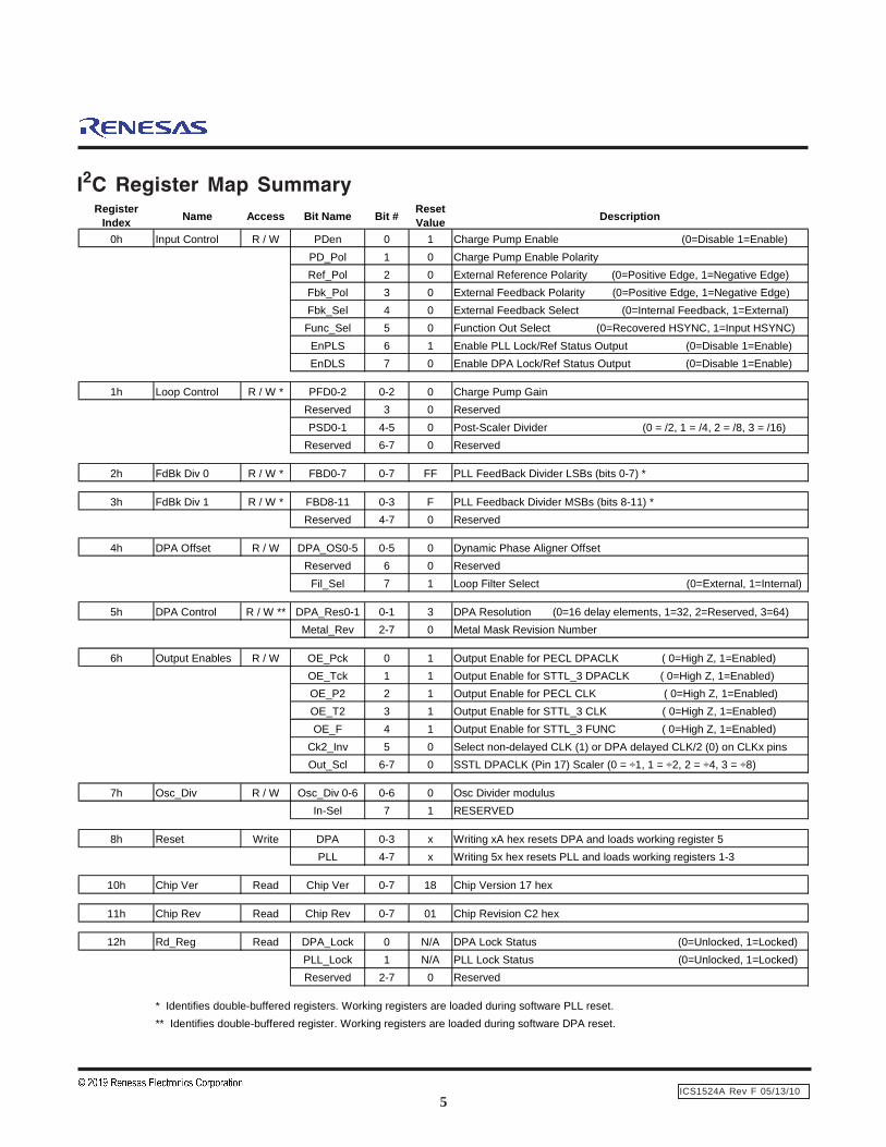
I2C Register Map SummaryRegister
Index Name Access Bit Name Bit # Reset Value Description
0h Input Control R / W PDen 0 1 Charge Pump Enable (0=Disable 1=Enable)PD_Pol 1 0 Charge Pump Enable Polarity Ref_Pol 2 0 External Reference Polarity (0=Positive Edge, 1=Negative Edge)Fbk_Pol 3 0 External Feedback Polarity (0=Positive Edge, 1=Negative Edge)Fbk_Sel 4 0 External Feedback Select (0=Internal Feedback, 1=External)Func_Sel 5 0 Function Out Select (0=Recovered HSYNC, 1=Input HSYNC)EnPLS 6 1 Enable PLL Lock/Ref Status Output (0=Disable 1=Enable)EnDLS 7 0 Enable DPA Lock/Ref Status Output (0=Disable 1=Enable)
1h Loop Control R / W * PFD0-2 0-2 0 Charge Pump GainReserved 3 0 ReservedPSD0-1 4-5 0 Post-Scaler Divider (0 = /2, 1 = /4, 2 = /8, 3 = /16)
Reserved 6-7 0 Reserved
2h FdBk Div 0 R / W * FBD0-7 0-7 FF PLL FeedBack Divider LSBs (bits 0-7) *
3h FdBk Div 1 R / W * FBD8-11 0-3 F PLL Feedback Divider MSBs (bits 8-11) *Reserved 4-7 0 Reserved
4h DPA Offset R / W DPA_OS0-5 0-5 0 Dynamic Phase Aligner OffsetReserved 6 0 Reserved
Fil_Sel 7 1 Loop Filter Select (0=External, 1=Internal)
5h DPA Control R / W ** DPA_Res0-1 0-1 3 DPA Resolution (0=16 delay elements, 1=32, 2=Reserved, 3=64)Metal_Rev 2-7 0 Metal Mask Revision Number
6h Output Enables R / W OE_Pck 0 1 Output Enable for PECL DPACLK ( 0=High Z, 1=Enabled)OE_Tck 1 1 Output Enable for STTL_3 DPACLK ( 0=High Z, 1=Enabled)OE_P2 2 1 Output Enable for PECL CLK ( 0=High Z, 1=Enabled)OE_T2 3 1 Output Enable for STTL_3 CLK ( 0=High Z, 1=Enabled)OE_F 4 1 Output Enable for STTL_3 FUNC ( 0=High Z, 1=Enabled)
Ck2_Inv 5 0 Select non-delayed CLK (1) or DPA delayed CLK/2 (0) on CLKx pinsOut_Scl 6-7 0 SSTL DPACLK (Pin 17) Scaler (0 = ÷1, 1 = ÷2, 2 = ÷4, 3 = ÷8)
7h Osc_Div R / W Osc_Div 0-6 0-6 0 Osc Divider modulusIn-Sel 7 1 RESERVED
8h Reset Write DPA 0-3 x Writing xA hex resets DPA and loads working register 5PLL 4-7 x Writing 5x hex resets PLL and loads working registers 1-3
10h Chip Ver Read Chip Ver 0-7 18 Chip Version 17 hex
11h Chip Rev Read Chip Rev 0-7 01 Chip Revision C2 hex
12h Rd_Reg Read DPA_Lock 0 N/A DPA Lock Status (0=Unlocked, 1=Locked)PLL_Lock 1 N/A PLL Lock Status (0=Unlocked, 1=Locked)Reserved 2-7 0 Reserved
* Identifies double-buffered registers. Working registers are loaded during software PLL reset.** Identifies double-buffered register. Working registers are loaded during software DPA reset.
ICS1524A
6
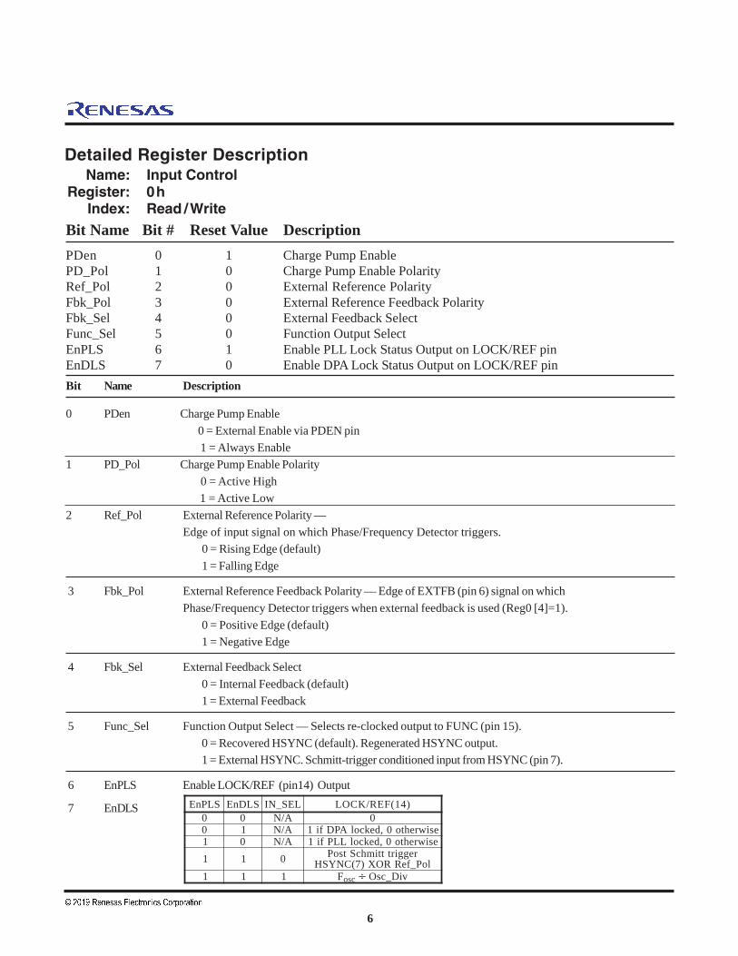
Detailed Register DescriptionName: Input Control
Register: 0hIndex: Read /Write
Bit Name Description
0 PDen Charge Pump Enable 0 = External Enable via PDEN pin 1 = Always Enable
1 PD_Pol Charge Pump Enable Polarity0 = Active High1 = Active Low
2 Ref_Pol External Reference Polarity —Edge of input signal on which Phase/Frequency Detector triggers.
0 = Rising Edge (default)1 = Falling Edge
3 Fbk_Pol External Reference Feedback Polarity — Edge of EXTFB (pin 6) signal on whichPhase/Frequency Detector triggers when external feedback is used (Reg0 [4]=1).
0 = Positive Edge (default)1 = Negative Edge
4 Fbk_Sel External Feedback Select0 = Internal Feedback (default)1 = External Feedback
5 Func_Sel Function Output Select — Selects re-clocked output to FUNC (pin 15).0 = Recovered HSYNC (default). Regenerated HSYNC output.1 = External HSYNC. Schmitt-trigger conditioned input from HSYNC (pin 7).
6 EnPLS Enable LOCK/REF (pin14) Output
7 EnDLS
Bit Name Bit # Reset Value DescriptionPDen 0 1 Charge Pump EnablePD_Pol 1 0 Charge Pump Enable PolarityRef_Pol 2 0 External Reference PolarityFbk_Pol 3 0 External Reference Feedback PolarityFbk_Sel 4 0 External Feedback SelectFunc_Sel 5 0 Function Output SelectEnPLS 6 1 Enable PLL Lock Status Output on LOCK/REF pinEnDLS 7 0 Enable DPA Lock Status Output on LOCK/REF pin
SLPnE SLDnE LES_NI )41(FER/KCOL0 0 A/N 00 1 A/N esiwrehto0,dekcolAPDfi11 0 A/N esiwrehto0,dekcolLLPfi11 1 0 reggirtttimhcStsoP
loP_feRROX)7(CNYSH1 1 1 F cso ÷ viD_csO
7
ICS1524A
ICS1524A Rev F 05/13/10
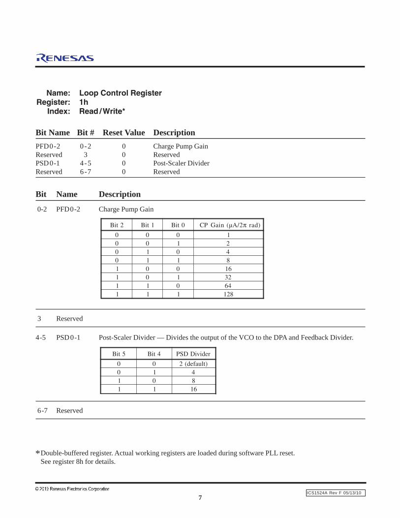
Name: Loop Control RegisterRegister: 1h
Index: Read /Write*
Bit Name Bit # Reset Value DescriptionPFD0-2 0-2 0 Charge Pump GainReserved 3 0 ReservedPSD0-1 4-5 0 Post-Scaler DividerReserved 6-7 0 Reserved
Bit Name Description
0-2 PFD0-2 Charge Pump Gain
3 Reserved
4-5 PSD0-1 Post-Scaler Divider — Divides the output of the VCO to the DPA and Feedback Divider.
6-7 Reserved
*Double-buffered register. Actual working registers are loaded during software PLL reset.See register 8h for details.
2tiB 1tiB 0tiB 2/Aµ(niaGCP π )dar
0 0 0 10 0 1 20 1 0 40 1 1 81 0 0 611 0 1 231 1 0 461 1 1 821
5tiB 4tiB rediviDDSP
0 0 )tluafed(20 1 41 0 81 1 61
ICS1524A
8
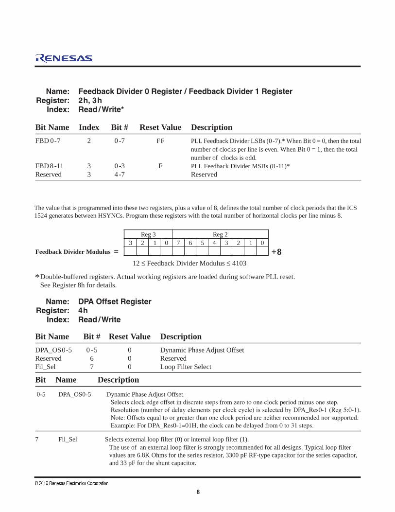
Name: Feedback Divider 0 Register / Feedback Divider 1 RegisterRegister: 2h, 3h
Index: Read /Write*
Bit Name Index Bit # Reset Value DescriptionFBD 0-7 2 0-7 FF PLL Feedback Divider LSBs (0-7).* When Bit 0 = 0, then the total
number of clocks per line is even. When Bit 0 = 1, then the totalnumber of clocks is odd.
FBD8-11 3 0-3 F PLL Feedback Divider MSBs (8 -11)*Reserved 3 4-7 Reserved
Feedback Divider Modulus =
*Double-buffered registers. Actual working registers are loaded during software PLL reset.See Register 8h for details.
Name: DPA Offset RegisterRegister: 4h
Index: Read /Write
Bit Name Bit # Reset Value DescriptionDPA_OS0-5 0-5 0 Dynamic Phase Adjust OffsetReserved 6 0 ReservedFil_Sel 7 0 Loop Filter Select
Bit Name Description
0-5 DPA_OS0-5 Dynamic Phase Adjust Offset.Selects clock edge offset in discrete steps from zero to one clock period minus one step.Resolution (number of delay elements per clock cycle) is selected by DPA_Res0-1 (Reg 5:0-1).Note: Offsets equal to or greater than one clock period are neither recommended nor supported.Example: For DPA_Res0-1=01H, the clock can be delayed from 0 to 31 steps.
7 Fil_Sel Selects external loop filter (0) or internal loop filter (1).The use of an external loop filter is strongly recommended for all designs. Typical loop filtervalues are 6.8K Ohms for the series resistor, 3300 pF RF-type capacitor for the series capacitor,and 33 pF for the shunt capacitor.
12 ≤ Feedback Divider Modulus ≤ 4103
The value that is programmed into these two registers, plus a value of 8, defines the total number of clock periods that the ICS1524 generates between HSYNCs. Program these registers with the total number of horizontal clocks per line minus 8.
3geR 2geR3 2 1 0 7 6 5 4 3 2 1 0
+8
9
ICS1524A
ICS1524A Rev F 05/13/10
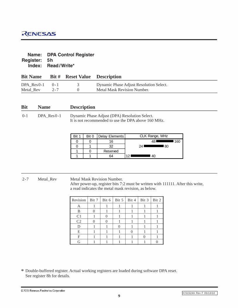
Name: DPA Control RegisterRegister: 5h
Index: Read /Write*
Bit Name Bit # Reset Value DescriptionDPA_Res0-1 0- 1 3 Dynamic Phase Adjust Resolution Select.Metal_Rev 2-7 0 Metal Mask Revision Number.
Bit Name Description
0-1 DPA_Res0-1 Dynamic Phase Adjust (DPA) Resolution Select.It is not recommended to use the DPA above 160 MHz.
2-7 Metal_Rev Metal Mask Revision Number.After power-up, register bits 7:2 must be written with 111111. After this write,a read indicates the metal mask revision, as below.
* Double-buffered register. Actual working registers are loaded during software DPA reset.See register 8h for details.
Bit 1 Bit 0 Delay Elements0 0 16 48 1600 1 32 24 801 0 Reserved1 1 64 12 40
CLK Range, MHz
noisiveR 7tiB 6tiB 5tiB 4tiB 3tiB 2tiBA 1 1 1 1 1 1B 0 1 1 1 1 11C 1 0 1 1 1 12C 0 0 1 1 1 1
D 1 1 0 1 1 1E 1 1 1 0 1 1F 1 1 1 1 0 1G 1 1 1 1 1 0
ICS1524A
10
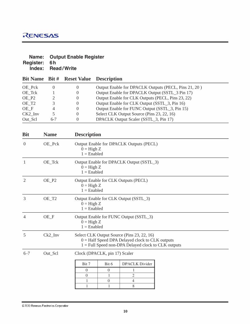
Name: Output Enable RegisterRegister: 6h
Index: Read /Write
Bit Name Bit # Reset Value DescriptionOE_Pck 0 0 Output Enable for DPACLK Outputs (PECL, Pins 21, 20 )OE_Tck 1 0 Output Enable for DPACLK Output (SSTL_3 Pin 17)OE_P2 2 0 Output Enable for CLK Outputs (PECL, Pins 23, 22)OE_T2 3 0 Output Enable for CLK Output (SSTL_3, Pin 16)OE_F 4 0 Output Enable for FUNC Output (SSTL_3, Pin 15)CK2_Inv 5 0 Select CLK Output Source (Pins 23, 22, 16)Out_Scl 6-7 0 DPACLK Output Scaler (SSTL_3, Pin 17)
Bit Name Description
0 OE_Pck Output Enable for DPACLK Outputs (PECL)0 = High Z1 = Enabled
1 OE_Tck Output Enable for DPACLK Output (SSTL_3)0 = High Z1 = Enabled
2 OE_P2 Output Enable for CLK Outputs (PECL)0 = High Z1 = Enabled
3 OE_T2 Output Enable for CLK Output (SSTL_3)0 = High Z1 = Enabled
4 OE_F Output Enable for FUNC Output (SSTL_3)0 = High Z1 = Enabled
5 Ck2_Inv Select CLK Output Source (Pins 23, 22, 16)0 = Half Speed DPA Delayed clock to CLK outputs1 = Full Speed non-DPA Delayed clock to CLK outputs
6-7 Out_Scl Clock (DPACLK, pin 17) Scaler
0 0 10 1 21 0 41 1 8
DPACLK DividerBit 7 Bit 6
11
ICS1524A
ICS1524A Rev F 05/13/10
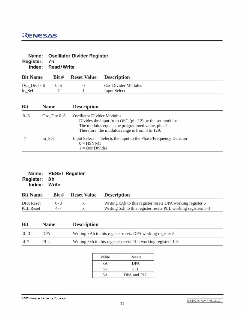
Name: Oscillator Divider RegisterRegister: 7h
Index: Read /Write
Bit Name Bit # Reset Value DescriptionOsc_Div 0-6 0-6 0 Osc Divider ModulusIn_Sel 7 1 Input Select
Bit Name Description
0-6 Osc_Div 0-6 Oscillator Divider Modulus.Divides the input from OSC (pin 12) by the set modulus.The modulus equals the programmed value, plus 2.Therefore, the modulus range is from 3 to 129.
7 In_Sel Input Select — Selects the input to the Phase/Frequency Detector0 = HSYNC1 = Osc Divider
Name: RESET RegisterRegister: 8h
Index: Write
Bit Name Bit # Reset Value DescriptionDPA Reset 0 -3 x Writing xAh to this register resets DPA working register 5PLL Reset 4 -7 x Writing 5xh to this register resets PLL working registers 1-3
Bit Name Description
0 -3 DPA Writing xAh to this register resets DPA working register 5
4 -7 PLL Writing 5xh to this register resets PLL working registers 1-3
eulaV steseRAx APDx5 LLPA5 LLPdnaAPD
ICS1524A
12
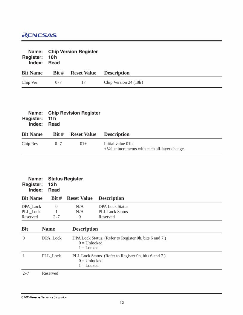
Name: Chip Version RegisterRegister: 10h
Index: Read
Bit Name Bit # Reset Value Description
Chip Ver 0-7 17 Chip Version 24 (18h)
Name: Chip Revision RegisterRegister: 11h
Index: Read
Bit Name Bit # Reset Value Description
Chip Rev 0 -7 01+ Initial value 01h.+Value increments with each all-layer change.
Name: Status RegisterRegister: 12h
Index: Read
Bit Name Bit # Reset Value DescriptionDPA_Lock 0 N/A DPA Lock StatusPLL_Lock 1 N/A PLL Lock StatusReserved 2-7 0 Reserved
Bit Name Description
0 DPA_Lock DPA Lock Status. (Refer to Register 0h, bits 6 and 7.)0 = Unlocked1 = Locked
1 PLL_Lock PLL Lock Status. (Refer to Register 0h, bits 6 and 7.)0 = Unlocked1 = Locked
2-7 Reserved
13
ICS1524A
ICS1524A Rev F 05/13/10
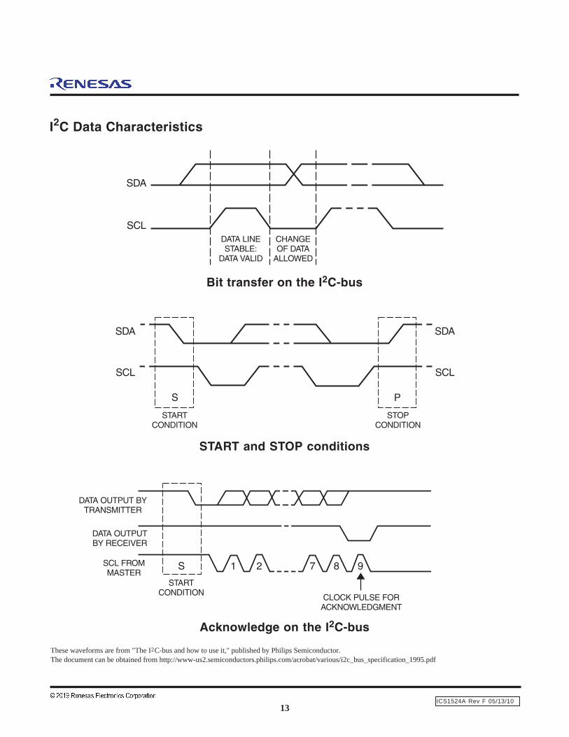
I2C Data Characteristics
Bit transfer on the I2C-bus
START and STOP conditions
Acknowledge on the I2C-bus
These waveforms are from "The I2C-bus and how to use it," published by Philips Semiconductor.The document can be obtained from http://www-us2.semiconductors.philips.com/acrobat/various/i2c_bus_specification_1995.pdf
ICS1524A
14
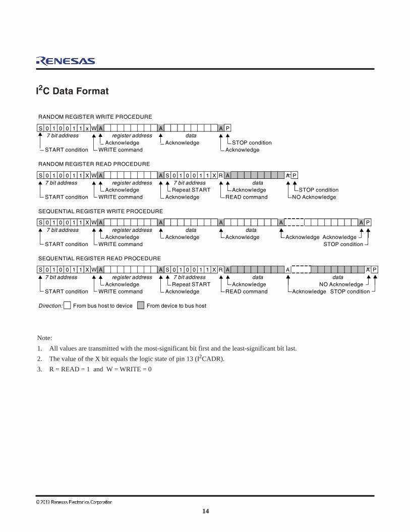
I2C Data Format
RANDOM REGISTER WRITE PROCEDURE
S 0 1 0 0 1 1 x W A A A P 7 bit address register address data
Acknowledge Acknowledge STOP conditionSTART condition WRITE command Acknowledge
RANDOM REGISTER READ PROCEDURE
S 0 1 0 0 1 1 X W A A S 0 1 0 0 1 1 X R A A P7 bit address register address 7 bit address data
Acknowledge Repeat START Acknowledge STOP conditionSTART condition WRITE command Acknowledge READ command NO Acknowledge
SEQUENTIAL REGISTER WRITE PROCEDURE
S 0 1 0 0 1 1 X W A A A A A P 7 bit address register address data data
Acknowledge Acknowledge Acknowledge Acknowledge AcknowledgeSTART condition WRITE command STOP condition
SEQUENTIAL REGISTER READ PROCEDURE
S 0 1 0 0 1 1 X W A A S 0 1 0 0 1 1 X R A A A P7 bit address register address 7 bit address data data
Acknowledge Repeat START Acknowledge NO AcknowledgeSTART condition WRITE command Acknowledge READ command Acknowledge STOP condition
Direction: From bus host to device From device to bus host
Note:1. All values are transmitted with the most-significant bit first and the least-significant bit last.2. The value of the X bit equals the logic state of pin 13 (I2CADR).3. R = READ = 1 and W = WRITE = 0
15
ICS1524A
ICS1524A Rev F 05/13/10
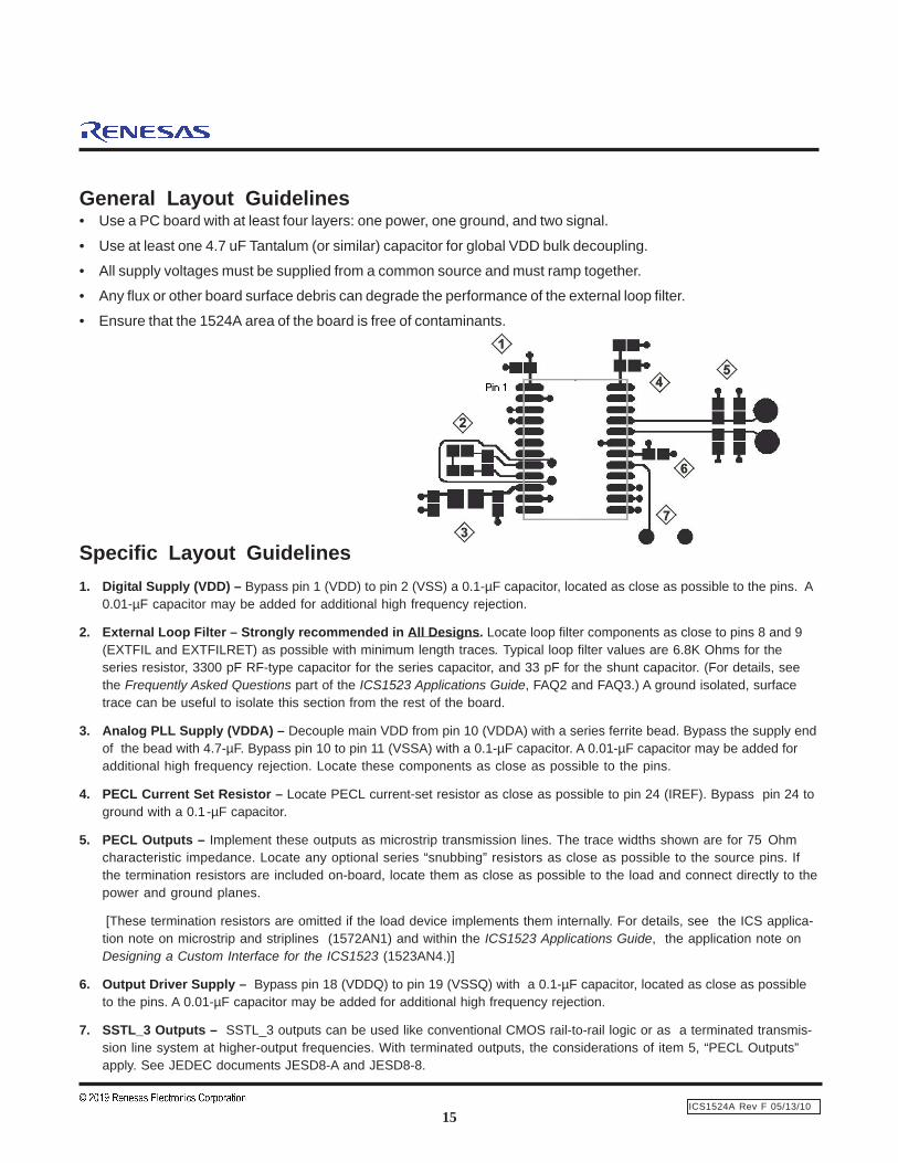
Specific Layout Guidelines1. Digital Supply (VDD) – Bypass pin 1 (VDD) to pin 2 (VSS) a 0.1-µF capacitor, located as close as possible to the pins. A
0.01-µF capacitor may be added for additional high frequency rejection.
2. External Loop Filter – Strongly recommended in All Designs. Locate loop filter components as close to pins 8 and 9(EXTFIL and EXTFILRET) as possible with minimum length traces. Typical loop filter values are 6.8K Ohms for theseries resistor, 3300 pF RF-type capacitor for the series capacitor, and 33 pF for the shunt capacitor. (For details, seethe Frequently Asked Questions part of the ICS1523 Applications Guide, FAQ2 and FAQ3.) A ground isolated, surfacetrace can be useful to isolate this section from the rest of the board.
3. Analog PLL Supply (VDDA) – Decouple main VDD from pin 10 (VDDA) with a series ferrite bead. Bypass the supply endof the bead with 4.7-µF. Bypass pin 10 to pin 11 (VSSA) with a 0.1-µF capacitor. A 0.01-µF capacitor may be added foradditional high frequency rejection. Locate these components as close as possible to the pins.
4. PECL Current Set Resistor – Locate PECL current-set resistor as close as possible to pin 24 (IREF). Bypass pin 24 toground with a 0.1 -µF capacitor.
5. PECL Outputs – Implement these outputs as microstrip transmission lines. The trace widths shown are for 75 Ohmcharacteristic impedance. Locate any optional series “snubbing” resistors as close as possible to the source pins. Ifthe termination resistors are included on-board, locate them as close as possible to the load and connect directly to thepower and ground planes.
[These termination resistors are omitted if the load device implements them internally. For details, see the ICS applica-tion note on microstrip and striplines (1572AN1) and within the ICS1523 Applications Guide, the application note onDesigning a Custom Interface for the ICS1523 (1523AN4.)]
6. Output Driver Supply – Bypass pin 18 (VDDQ) to pin 19 (VSSQ) with a 0.1-µF capacitor, located as close as possibleto the pins. A 0.01-µF capacitor may be added for additional high frequency rejection.
7. SSTL_3 Outputs – SSTL_3 outputs can be used like conventional CMOS rail-to-rail logic or as a terminated transmis-sion line system at higher-output frequencies. With terminated outputs, the considerations of item 5, “PECL Outputs”apply. See JEDEC documents JESD8-A and JESD8-8.
.
General Layout Guidelines• Use a PC board with at least four layers: one power, one ground, and two signal.
• Use at least one 4.7 uF Tantalum (or similar) capacitor for global VDD bulk decoupling.
• All supply voltages must be supplied from a common source and must ramp together.
• Any flux or other board surface debris can degrade the performance of the external loop filter.
• Ensure that the 1524A area of the board is free of contaminants.
ICS1524A
16
PECL OutputsFor information on using the ICS1524A’s PECL output pins, please refer to Application Note 4: Designing a CustomPECL Interface for the ICS1523
SSTL_3 OutputsUnterminated OutputsIn the ICS1524A, unterminated SSTL_3 output pins display exponential transitions similar to those of rectangularpulses presented to RC loads. The 10-90% rise time is typically 1.6 ns, and the corresponding fall time is typically700 ps. In turn, this asymmetry contributes to duty cycle asymmetry at higher output frequencies. In the absence ofsignificant load capacitance (which can further increase rise and fall time), this asymmetry is the dominant factordetermining high-frequency performance of these single-ended outputs. Typically, no termination is required either forthe LOCK/REF, FUNC, and CLK/2 outputs or for CLK outputs up to approximately 135 MHz.
Terminated OutputsSSTL_3 outputs are intended to terminate in low impedances to reduce the effect of external circuit capacitance.Use of transmission line techniques enables use of longer traces between source and driver without increasingringing due to reflections. Where external capacitance is minimal and substantial voltage swing is required to meetLVTTL VIH and VOL requirements, the intrinsic rise and fall times of ICS1524A SSTL outputs are only slightly improvedby termination in a low impedance.
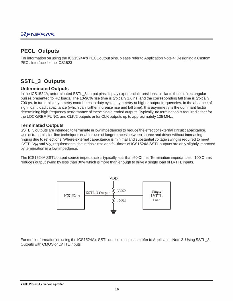
The ICS1524A SSTL output source impedance is typically less than 60 Ohms. Termination impedance of 100 Ohmsreduces output swing by less than 30% which is more than enough to drive a single load of LVTTL inputs.
For more information on using the ICS1524A’s SSTL output pins, please refer to Application Note 3: Using SSTL_3Outputs with CMOS or LVTTL Inputs
ICS1524A
VDD
SSTL-3 Output 330Ω
150Ω
SingleLVTTL
Load
17
ICS1524A
ICS1524A Rev F 05/13/10
Absolute Maximum Ratings
VDD, VDDA, VDDQ (measured to VSS) . . . . . . . . . . . . . . . . . 4.3 VDigital Inputs . . . . . . . . . . . . . . . . . . . . . . . . . . . . . . . . . . . . . . . . VSS – 0.3 V to 5.5 VAnalog Outputs . . . . . . . . . . . . . . . . . . . . . . . . . . . . . . . . . . . . . . . VSSA – 0.3 V to VDDA +0.3 VDigital Outputs . . . . . . . . . . . . . . . . . . . . . . . . . . . . . . . . . . . . . . . VSSQ – 0.3 V to VDDQ +0.3 VStorage Temperature . . . . . . . . . . . . . . . . . . . . . . . . . . . . . . . . . . . – 65°C to +150°CJunction Temperature . . . . . . . . . . . . . . . . . . . . . . . . . . . . . . . . . . 175°CSoldering Temperature . . . . . . . . . . . . . . . . . . . . . . . . . . . . . . . . . 260°CESD Susceptibility* . . . . . . . . . . . . . . . . . . . . . . . . . . . . . . . . . . > 2 KV(*Electrostatic-sensitive devices. Do not open or handle except in a static-free workstation.)
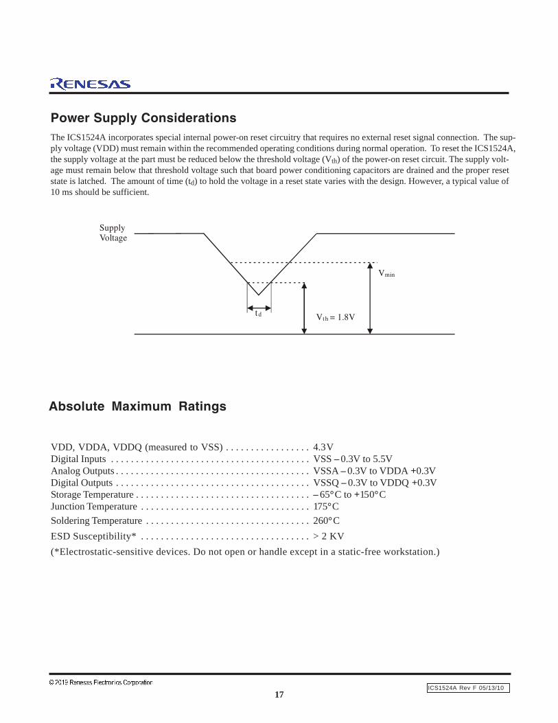
Power Supply ConsiderationsThe ICS1524A incorporates special internal power-on reset circuitry that requires no external reset signal connection. The sup-ply voltage (VDD) must remain within the recommended operating conditions during normal operation. To reset the ICS1524A,the supply voltage at the part must be reduced below the threshold voltage (Vth) of the power-on reset circuit. The supply volt-age must remain below that threshold voltage such that board power conditioning capacitors are drained and the proper resetstate is latched. The amount of time (td) to hold the voltage in a reset state varies with the design. However, a typical value of10 ms should be sufficient.
Supply Voltage
td V = 1.8Vth
Vmin
ICS1524A
18
Recommended Operating Conditions
VDD, VDDQ, VDDA (measured to VSS) . 3.0 to 3.6 VOperating Temperature (Ambient) . . . . . . 0 to +70°C
tnerruCylppuSCD
RETEMARAP LOBMYS SNOITIDNOC NIM XAM STINUlatigiD,tnerruCylppuS DDDI V6.3=DDDV — 52 Am
srevirDtuptuO,tnerruCylppuS QDDI .delbanesrevirdtuptuoon,V6.3=QDDV — 6 AmgolanA,tnerruCylppuS ADDI V6.3=ADDV — 5 Am
,CSO,CNYSH,BFTXE,NEDP,LCS,ADS(stupnIlatigiD I2C )RDARETEMARAP LOBMYS SNOITIDNOC NIM XAM STINU
egatloVhgiHtupnI HIV 2 5.5 VegatloVwoLtupnI LIV 3.0-SSV 8.0 V
siseretsyHtupnI 2.0 6.0 VtnerruChgiHtupnI HII V HI DDV= — 01± AµtnerruCwoLtupnI LII V LI 0= — 002± Aµ
ecnaticapaCtupnI niC — 01 Fp
)lanoitceridiBsiADS:edoMtuptuOnI(ADSRETEMARAP LOBMYS SNOITIDNOC NIM XAM STINU
egatloVwoLtuptuO LOV samumixamV0.6=HOV.Am3=TUOI.rotsiserpu-lluplanretxeehtybdenimreted 4.0 V
KLC,+KLC,–KLCAPD,+KLCAPD(stuptuOLCEP )-RETEMARAP LOBMYS SNOITIDNOC NIM XAM STINU
egatloVhgiHtuptuO HOV 0=TUOI — DDV VycneuqerFtuptuOmumixaM XAMpF V3.3=DDDV — 052 zHM
egatloVwoLtuptuOwolebllaftontsumLOV:etoN(
tcerrocehttahtosneviglevelehtebnacTUOIrofeulav
).deniatniam
LOV eulavdemmargorp=TUOI 0.1 — V
(stuptuO3-LTSS APD KCOL,CNUF,KLC,KLC )FER/RETEMARAP LOBMYS SNOITIDNOC NIM XAM STINU
ecnatsiseRtuptuO RO V<1 O V2< — 08 ΩycneuqerFtuptuOmumixaM XAMsF V3.3=DDDV — 051 zHM
scitsiretcarahCtupnICARETEMARAP LOBMYS SNOITIDNOC NIM XAM STINUycneuqerFtupnICNYSH f CNYSH 800. 01 zHM
ycneuqerFtupnICSO f CSO 20. 001 zHM
19
ICS1524A
ICS1524A Rev F 05/13/10
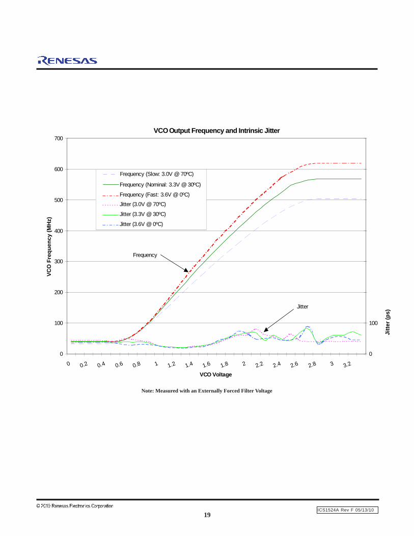
VCO Output Frequency and Intrinsic Jitter
0
100
200
300
400
500
600
700
0 0.2 0.4 0.6 0.8 1 1.2 1.4 1.6 1.8 2 2.2 2.4 2.6 2.8 3 3.2
VCO Voltage
VCO
Fre
quen
cy (M
Hz)
0
100
200
300
400
500
600
700
Jitte
r (ps
)
Frequency (Slow: 3.0V @ 70ºC)
Frequency (Nominal: 3.3V @ 30ºC)
Frequency (Fast: 3.6V @ 0ºC)Jitter (3.0V @ 70ºC)
Jitter (3.3V @ 30ºC)
Jitter (3.6V @ 0ºC)
Frequency
Jitter
Note: Measured with an Externally Forced Filter Voltage
ICS1524A
20
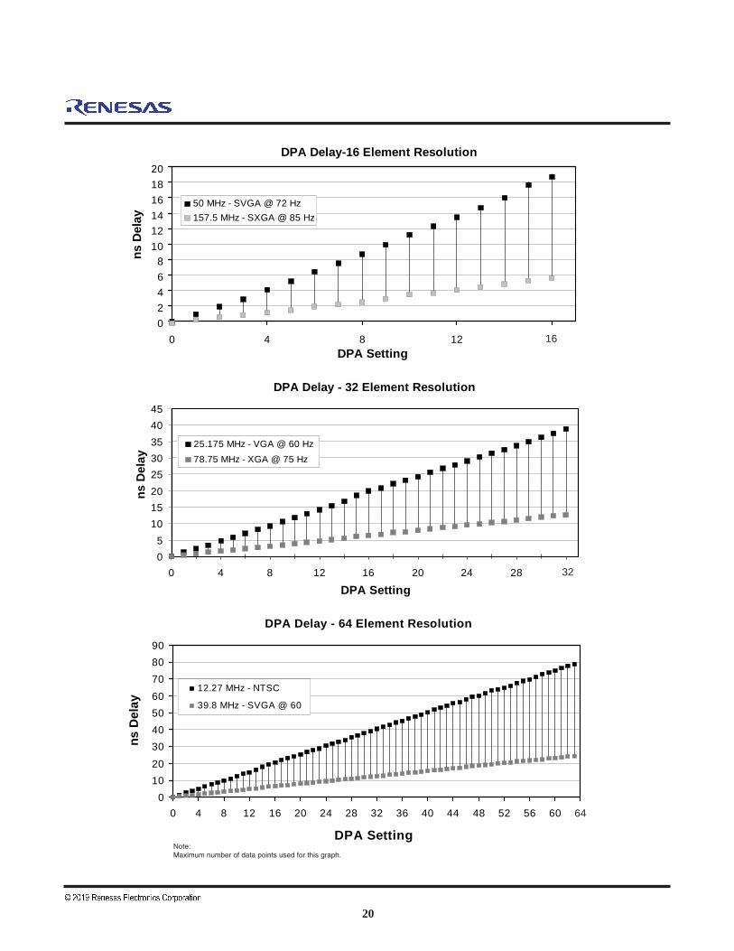
DPA Delay-16 Element Resolution
02468
101214161820
0 4 8 12DPA Setting
ns D
elay
50 MHz - SVGA @ 72 Hz157.5 MHz - SXGA @ 85 Hz
DPA Delay - 32 Element Resolution
05
1015202530354045
0 4 8 12 16 20 24 28
DPA Setting
ns D
elay
25.175 MHz - VGA @ 60 Hz78.75 MHz - XGA @ 75 Hz
16
DPA Delay - 64 Element Resolution
0102030405060708090
0 4 8 12 16 20 24 28 32 36 40 44 48 52 56 60
DPA Setting
ns D
elay
12.27 MHz - NTSC
39.8 MHz - SVGA @ 60
32
64
Note:Maximum number of data points used for this graph.
21
ICS1524A
ICS1524A Rev F 05/13/10
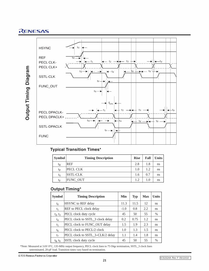
Ou
tpu
t T
imin
g D
iag
ram
lobmyS noitpircseDgnimiT niM pyT xaM stinU
t0 yaledFERotCNYSH 3.11 5.11 21 snt1 yaledkcolcLCEPotFER 0.1- 8.0 2.2 sn
t2 t, 3 elcycytudkcolcLCEP 54 05 55 %t4 yaledkcolc3_LTSSotkcolcLCEP 2.0 57.0 2.1 snt5 yaledTUO_CNUFotkcolcLCEP 5.1 9.1 3.2 snt6 kcolc2/LCEPotkcolcLCEP 0.1 3.1 5.1 snt7 yaled2/KLC–3_LTSSotkcolcLCEP 1.1 4.1 8.1 sn
t8 t, 9 elcycytudkcolcLTSS 54 05 55 %
*Note: Measured at 3.6V 0°C, 135-MHz output frequency, PECL clock lines to 75 Οηµ termination, SSTL_3 clock linesunterminated, 20-pF load. Transition times vary based on termination.
Typical Transition Times*
Output Timing*
REF
HSYNC
PECL CLK-PECL CLK+
SSTL-CLK
FUNC_OUT
t0
tR
tS
tF
t5
t4 t8 t9
t1 t2 t3 tp
PECL DPACLK-PECL DPACLK+
SSTL-DPACLK
FUNC
tDPA
t8 t9tS
tF
t4
t1 t2 t3 tp
lobmyS noitpircseDgnimiT esiR llaF stinU
tR FER 8.2 8.1 sntP KLCLCEP 0.1 2.1 sntS KLC-LTSS 6.1 7.0 sntF TUO_CNUF 2.1 0.1 sn
ICS1524A
22
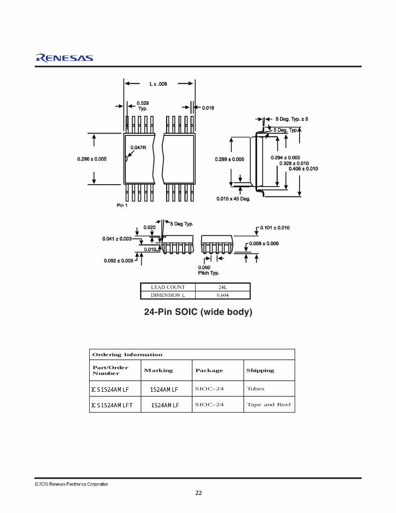
24-Pin SOIC (wide body)
noitamrofnIgniredrO
redrO/traPrebmuN gnikraM egakcaP gnippihS
M4251SCI M4251SCI 42-COIS sebuT
TM4251SCI M4251SCI 42-COIS leeRdnaepaT
millerm
Text Box
ICS1524AM
millerm
Text Box
ICS1524AMT
millerm
Text Box
1524AM
millerm
Text Box
1524AM
millerm
Text Box
millerm
Text Box
ICS1524AMLF
millerm
Text Box
ICS1524AMLFT
millerm
Text Box
1524AMLF
millerm
Text Box
1524AMLF
23
ICS1524A
ICS1524A Rev D 12/23/2005
NOTES

ICS1524A
24
Corporate HeadquartersTOYOSU FORESIA, 3-2-24 Toyosu,Koto-ku, Tokyo 135-0061, Japanwww.renesas.com
Contact InformationFor further information on a product, technology, the most up-to-date version of a document, or your nearest sales office, please visit:www.renesas.com/contact/
TrademarksRenesas and the Renesas logo are trademarks of Renesas Electronics Corporation. All trademarks and registered trademarks are the property of their respective owners.
IMPORTANT NOTICE AND DISCLAIMER
RENESAS ELECTRONICS CORPORATION AND ITS SUBSIDIARIES (“RENESAS”) PROVIDES TECHNICAL SPECIFICATIONS AND RELIABILITY DATA (INCLUDING DATASHEETS), DESIGN RESOURCES (INCLUDING REFERENCE DESIGNS), APPLICATION OR OTHER DESIGN ADVICE, WEB TOOLS, SAFETY INFORMATION, AND OTHER RESOURCES “AS IS” AND WITH ALL FAULTS, AND DISCLAIMS ALL WARRANTIES, EXPRESS OR IMPLIED, INCLUDING, WITHOUT LIMITATION, ANY IMPLIED WARRANTIES OF MERCHANTABILITY, FITNESS FOR A PARTICULAR PURPOSE, OR NON-INFRINGEMENT OF THIRD PARTY INTELLECTUAL PROPERTY RIGHTS.
These resources are intended for developers skilled in the art designing with Renesas products. You are solely responsible for (1) selecting the appropriate products for your application, (2) designing, validating, and testing your application, and (3) ensuring your application meets applicable standards, and any other safety, security, or other requirements. These resources are subject to change without notice. Renesas grants you permission to use these resources only for development of an application that uses Renesas products. Other reproduction or use of these resources is strictly prohibited. No license is granted to any other Renesas intellectual property or to any third party intellectual property. Renesas disclaims responsibility for, and you will fully indemnify Renesas and its representatives against, any claims, damages, costs, losses, or liabilities arising out of your use of these resources. Renesas' products are provided only subject to Renesas' Terms and Conditions of Sale or other applicable terms agreed to in writing. No use of any Renesas resources expands or otherwise alters any applicable warranties or warranty disclaimers for these products.
(Rev.1.0 Mar 2020)
© 2020 Renesas Electronics Corporation. All rights reserved.