EL4544 Datasheet - Renesas Electronics
26
FN7362 Rev 5.00 Page 1 of 26 February 23, 2012 FN7362 Rev 5.00 February 23, 2012 EL4544 Triple 16x5 Differential Crosspoint Switch Capable of Operation in Single-Ended or Differential Input Modes DATASHEET The EL4544 is a high bandwidth 16-channel differential RGB to 5-channel RGB single-ended RGB-HV video crosspoint switch with embedded sync extraction. There are four 16-Channel input muxes, each capable of receiving a complete RGB video signal, and five output muxes, each capable of “seeing” any one of the four RGB inputs. Additionally, the fifth input mux has an overlay “screen on screen” function that can be displayed in conjunction with any of the stacked RGB inputs. The EL4544 has a fast disable feature to reduce power consumption. The device also provides a presence of signal indicator by looking for syncs on a designated channel. Features • Serial programming of switch array • Parallel or serial modes • High Z output disable • Drives 150 loads • 60MHz 0.1dB gain flatness • -3dB bandwidth of 300MHz • Crosstalk rejection: 75dB @ 100MHz • Channels settle to 5% within 10ns after overlay switching • 356 pin PBGA packaging • Pb-free (RoHS compliant) Applications • Video switching Ordering Information PART NUMBER (Note) PART MARKING PACKAGE (Pb-Free) PKG. DWG. # EL4544IGZ EL4544IGZ 356 Pin (27x27mm) PBGA V356.27x27B NOTE: These Intersil Pb-free WLCSP and BGA packaged products employ special Pb-free material sets; molding compounds/die attach materials and SnAgCu - e1 solder ball terminals, which are RoHS compliant and compatible with both SnPb and Pb-free soldering operations. Intersil Pb-free WLCSP and BGA packaged products are MSL classified at Pb-free peak reflow temperatures that meet or exceed the Pb-free requirements of IPC/JEDEC J STD-020.
Transcript of EL4544 Datasheet - Renesas Electronics

FN7362Rev 5.00
February 23, 2012
EL4544Triple 16x5 Differential Crosspoint Switch Capable of Operation in Single-Ended or Differential Input Modes
DATASHEET
The EL4544 is a high bandwidth 16-channel differential RGB to 5-channel RGB single-ended RGB-HV video crosspoint switch with embedded sync extraction. There are four 16-Channel input muxes, each capable of receiving a complete RGB video signal, and five output muxes, each capable of “seeing” any one of the four RGB inputs. Additionally, the fifth input mux has an overlay “screen on screen” function that can be displayed in conjunction with any of the stacked RGB inputs.
The EL4544 has a fast disable feature to reduce power consumption. The device also provides a presence of signal indicator by looking for syncs on a designated channel.
Features
• Serial programming of switch array
• Parallel or serial modes
• High Z output disable
• Drives 150 loads
• 60MHz 0.1dB gain flatness
• -3dB bandwidth of 300MHz
• Crosstalk rejection: 75dB @ 100MHz
• Channels settle to 5% within 10ns after overlay switching
• 356 pin PBGA packaging
• Pb-free (RoHS compliant)
Applications
• Video switching
Ordering InformationPART
NUMBER(Note)
PARTMARKING
PACKAGE(Pb-Free) PKG. DWG. #
EL4544IGZ EL4544IGZ 356 Pin (27x27mm) PBGA V356.27x27B
NOTE: These Intersil Pb-free WLCSP and BGA packaged products employ special Pb-free material sets; molding compounds/die attach materials and SnAgCu - e1 solder ball terminals, which are RoHS compliant and compatible with both SnPb and Pb-free soldering operations. Intersil Pb-free WLCSP and BGA packaged products are MSL classified at Pb-free peak reflow temperatures that meet or exceed the Pb-free requirements of IPC/JEDEC J STD-020.
FN7362 Rev 5.00 Page 1 of 26February 23, 2012

EL4544
PinoutEL4544
(356 PIN PBGA)TOP VIEW
20
19
18
17
16
15
14
13
12
11
10
9
8
7
6
5
4
2
3
1
A B C D E F G H J K L M N P R T U V W Y
Vp Vm BpF BpE BpD BpC BpB BpA Bp9 Bp8 Bp7 Bp6 Bp5 Bp4 Bp3 Bp2 Bp1 Bp0 Vm Vp
Vm Vm BnF BnE BnD BnC BnB BnA Bn9 Bn8 Bn7 Bn6 Bn5 Bn4 Bn3 Bn2 Bn1 Bn0 Vm Vm
RpF RnF TMon1 Vm Vm Vm Vm Vm Vm Vp Vm Vm Vm Vm Vm Vm Vm TMon2 GnF GpF
RpE RnE Vm Vm Vm Vm Vm Vm Vm Vm Vm Vm Vm Vm Vm Vm Vm Vm GnE GpE
RpD RnD Vm Vm Vm Vm GnD GpD
RpC RnC Vm Vm Vm Vm Vm Vm Vm Vm Vm Vm Vm Vm Vm Vm GnC GpC
RpB RnB Vm Vm Vm Vm Vm Vm Vm Vm Vm Vm Vm Vm Vm Vm GnB GpB
RpA RnA Vm Vm Vm Vm Vm Vm Vm Vm Vm Vm Vm Vm Vm Vm GnA GpA
Rp9 Rn9 Vm Vm Vm Vm Vm Vm Vm Vm Vm Vm Vm Vm Vm Vm Gn9 Gp9
Rp8 Rn8 Vp Vm Vm Vm Vm Vm Vm Vm Vm Vm Vm Vm Vm Vp Gn8 Gp8
Rp7 Rn7 Vm Vm Vm Vm Vm Vm Vm Vm Vm Vm Vm Vm Vm Vm Gn7 Gp7
Rp6 Rn6 Vm Vm Vm Vm Vm Vm Vm Vm Vm Vm Vm Vm Vm Vm Gn6 Gp6
Rp5 Rn5 Vm Vm Vm Vm Vm Vm Vm Vm Vm Vm Vm Vm Vm Vm Gn5 Gp5
Rp4 Rn4 Vm Vm Vm Vm Vm Vm Vm Vm Vm Vm Vm Vm Vm Vm Gn4 Gp4
Rp3 Rn3 RAZ GAZ Vm Vm Vm Vm Vm Vm Vm Vm Vm Vm NC NC Gn3 Gp3
Rp2 Rn2 Trans RefOL Vdp Chip Gn2 Gp2
Rp1 Rn1 Cal ROL BAZ Vm Vm Vm Vm Vm Vm Vm Vm Vm sEn Reset Gn1 Gp1GOL sDo
Rp0 Rn0 Vp Ovl Vm Vm Vm Vm Vm Vm Vm Vm Vm Vm sClk Vp Gn0 Gp0BOL sDi
VpS Hs Vs VmS Hd Vd VmD VpC Hc Vc VmC VpB Hb Vb VpA Ha Va VmAVpD VmB
Rs Gs Bs RefS Gd Bd RefD Rc Gc Bc RefC Rb Gb Bb Ra Ga Ba RefARd RefB
= EMPTY LOCATION (UNPOPULATED)= BALLGRID
FN7362 Rev 5.00 Page 2 of 26February 23, 2012

EL4544
Pin Descriptions
PIN NAME SOLDER BALL DESCRIPTION EQUIVALENT CIRCUIT
Rp0 A3 Red plus input 0
Rn0 B3 Red minus input 0 Reference Circuit 1
Rp1 A4 Red plus input 1 Reference Circuit 1
Rn1 B4 Red minus input 1 Reference Circuit 1
Rp2 A5 Red plus input 2 Reference Circuit 1
Rn2 B5 Red minus input 2 Reference Circuit 1
Rp3 A6 Red plus input 3 Reference Circuit 1
Rn3 B6 Red minus input 3 Reference Circuit 1
Rp4 A7 Red plus input 4 Reference Circuit 1
Rn4 B7 Red minus input 4 Reference Circuit 1
Rp5 A8 Red plus input 5 Reference Circuit 1
Rn5 B8 Red minus input 5 Reference Circuit 1
Rp6 A9 Red plus input 6 Reference Circuit 1
Rn6 B9 Red minus input 6 Reference Circuit 1
Rp7 A10 Red plus input 7 Reference Circuit 1
Rn7 B10 Red minus input 7
Vm Multiple Balls Analog minus supply
Vp C11 Analog plus supply Reference Circuit 1
Rp8 A11 Red plus input 8 Reference Circuit 1
Rn8 B11 Red minus input 8 Reference Circuit 1
Rp9 A12 Red plus input 9 Reference Circuit 1
Rn9 B12 Red minus input 9 Reference Circuit 1
RpA A13 Red plus input 10 Reference Circuit 1
RnA B13 Red minus input 10 Reference Circuit 1
RpB A14 Red plus input 11 Reference Circuit 1
RnB B14 Red minus input 11 Reference Circuit 1
RpC A15 Red plus input 12 Reference Circuit 1
RnC B15 Red minus input 12 Reference Circuit 1
RpD A16 Red plus input 13 Reference Circuit 1
RnD B16 Red minus input 13 Reference Circuit 1
RpE A17 Red plus input 14 Reference Circuit 1
RnE B17 Red minus input 14 Reference Circuit 1
RpF A18 Red plus input 15 Reference Circuit 1
RnF B18 Red minus input 15 Reference Circuit 1
VP
1.75k
VM
+–
VM
VREF1.5V
CIRCUIT 1
FN7362 Rev 5.00 Page 3 of 26February 23, 2012
EL4544
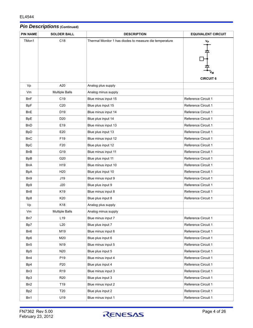
TMon1 C18 Thermal Monitor 1 has diodes to measure die temperature
Vp A20 Analog plus supply
Vm Multiple Balls Analog minus supply
BnF C19 Blue minus input 15 Reference Circuit 1
BpF C20 Blue plus input 15 Reference Circuit 1
BnE D19 Blue minus input 14 Reference Circuit 1
BpE D20 Blue plus input 14 Reference Circuit 1
BnD E19 Blue minus input 13 Reference Circuit 1
BpD E20 Blue plus input 13 Reference Circuit 1
BnC F19 Blue minus input 12 Reference Circuit 1
BpC F20 Blue plus input 12 Reference Circuit 1
BnB G19 Blue minus input 11 Reference Circuit 1
BpB G20 Blue plus input 11 Reference Circuit 1
BnA H19 Blue minus input 10 Reference Circuit 1
BpA H20 Blue plus input 10 Reference Circuit 1
Bn9 J19 Blue minus input 9 Reference Circuit 1
Bp9 J20 Blue plus input 9 Reference Circuit 1
Bn8 K19 Blue minus input 8 Reference Circuit 1
Bp8 K20 Blue plus input 8 Reference Circuit 1
Vp K18 Analog plus supply
Vm Multiple Balls Analog minus supply
Bn7 L19 Blue minus input 7 Reference Circuit 1
Bp7 L20 Blue plus input 7 Reference Circuit 1
Bn6 M19 Blue minus input 6 Reference Circuit 1
Bp6 M20 Blue plus input 6 Reference Circuit 1
Bn5 N19 Blue minus input 5 Reference Circuit 1
Bp5 N20 Blue plus input 5 Reference Circuit 1
Bn4 P19 Blue minus input 4 Reference Circuit 1
Bp4 P20 Blue plus input 4 Reference Circuit 1
Bn3 R19 Blue minus input 3 Reference Circuit 1
Bp3 R20 Blue plus input 3 Reference Circuit 1
Bn2 T19 Blue minus input 2 Reference Circuit 1
Bp2 T20 Blue plus input 2 Reference Circuit 1
Bn1 U19 Blue minus input 1 Reference Circuit 1
Pin Descriptions (Continued)
PIN NAME SOLDER BALL DESCRIPTION EQUIVALENT CIRCUIT
CIRCUIT 6
VP
VM
FN7362 Rev 5.00 Page 4 of 26February 23, 2012

EL4544
Bp1 U20 Blue plus input 1 Reference Circuit 1
Bn0 V19 Blue minus input 0 Reference Circuit 1
Bp0 V20 Blue plus input 0 Reference Circuit 1
Vm Vm Analog minus supply
Vp Y20 Analog plus supply
TMon2 V18 Thermal Monitor 2 has diodes to measure die temperature Reference Circuit 6
GnF W18 Green minus input 15 Reference Circuit 1
GpF Y18 Green plus input 15 Reference Circuit 1
GnE W17 Green minus input 14 Reference Circuit 1
GpE Y17 Green plus input 14 Reference Circuit 1
GnD W16 Green minus input 13 Reference Circuit 1
GpD Y16 Green plus input 13 Reference Circuit 1
GnC W15 Green minus input 12 Reference Circuit 1
GpC Y15 Green plus input 12 Reference Circuit 1
GnB W14 Green minus input 11 Reference Circuit 1
GpB Y14 Green plus input 11 Reference Circuit 1
GnA W13 Green minus input 10 Reference Circuit 1
GpA Y13 Green plus input 10 Reference Circuit 1
Gn9 W12 Green minus input 9 Reference Circuit 1
Gp9 Y12 Green plus input 9 Reference Circuit 1
Gn8 W11 Green minus input 8 Reference Circuit 1
Gp8 Y11 Green plus input 8 Reference Circuit 1
Vp V11 Analog plus supply
Vm Multiple Balls Analog minus supply
Gn7 W10 Green minus input 7 Reference Circuit 1
Gp7 Y10 Green plus input 7 Reference Circuit 1
Gn6 W9 Green minus input 6 Reference Circuit 1
Gp6 Y9 Green plus input 6 Reference Circuit 1
Gn5 W8 Green minus input 5 Reference Circuit 1
Gp5 Y8 Green plus input 5 Reference Circuit 1
Gn4 W7 Green minus input 4 Reference Circuit 1
Gp4 Y7 Green plus input 4 Reference Circuit 1
Gn3 W6 Green minus input 3 Reference Circuit 1
Gp3 Y6 Green plus input 3 Reference Circuit 1
Gn2 W5 Green minus input 2 Reference Circuit 1
Gp2 Y5 Green plus input 2 Reference Circuit 1
Gn1 W4 Green minus input 1 Reference Circuit 1
Gp1 Y4 Green plus input 1 Reference Circuit 1
Gn0 W3 Green minus input 0 Reference Circuit 1
Gp0 Y3 Green plus input 0 Reference Circuit 1
Pin Descriptions (Continued)
PIN NAME SOLDER BALL DESCRIPTION EQUIVALENT CIRCUIT
FN7362 Rev 5.00 Page 5 of 26February 23, 2012

EL4544
Vm Vm Analog minus supply
Vp V3 Analog plus supply
Chip V5 Chip enable (active low): when "HI" disables all analog except references; all analog or digital video outputs are in a high impedance state; all registers hold their data but remain programmable since the serial interface is left active
Vdp U5 Digital logic power supply: nominally at 3V
Reset V4 Reset (active low): clears all registers in interface and calibration sections; this causes the chip to standby with all outputs in a high impedance state
Reference Circuit 4
sEn U4 Serial bus enable (active low): enables the serial bus when "LO"; latches the current value when transitioning to "HI"
Reference Circuit 4
Vp V3 Analog plus supply
Vm Multiple Balls Analog minus supply
sClk U3 Serial bus clock Reference Circuit 4
sDo T4 Serial bus data output Reference Circuit 4
sDi T3 Serial bus data input
RefA Y1 Output stage reference level (input) A Reference Circuit 6
VmA Y2 RGB video output stages' minus supply A
Ba W1 Blue output A
Pin Descriptions (Continued)
PIN NAME SOLDER BALL DESCRIPTION EQUIVALENT CIRCUIT
CIRCUIT 4
VDP
VM VM
CIRCUIT 5
VDP
VM
CIRCUIT 7
VP
35k
VM VM
CIRCUIT 2
VP
VM
FN7362 Rev 5.00 Page 6 of 26February 23, 2012
EL4544
Va W2 Vertical sync output A Reference Circuit 5
Ga V1 Green output A Reference Circuit 2
Ha V2 Horizontal sync output A Reference Circuit 5
Ra U1 Red output A Reference Circuit 2
VpA U2 RGB video output stages' plus supply A Reference Circuit 7
RefB T1 Output stage reference level (input) B Reference Circuit 6
VmB T2 RGB video output stages' minus supply B Reference Circuit 7
Bb R1 Blue output B Reference Circuit 2
Vb R2 Vertical sync output B Reference Circuit 5
Gb P1 Green output B Reference Circuit 2
Hb P2 Horizontal sync output B Reference Circuit 5
Rb N1 Red output B Reference Circuit 2
VpB N2 RGB video output stages' plus supply B Reference Circuit 7
RefC M1 Output stage reference level (input) C Reference Circuit 6
VmC M2 RGB video output stages' minus supply C Reference Circuit 7
Bc L1 Blue output C Reference Circuit 2
Vc L2 Vertical sync output C Reference Circuit 5
Gc K1 Green output C Reference Circuit 2
Hc K2 Horizontal sync output C Reference Circuit 5
Rc J1 Red output C Reference Circuit 2
VpC J2 RGB video output stages' plus supply C Reference Circuit 7
RefD H1 Output stage reference level (input) D Reference Circuit 6
VmD H2 RGB video output stages' minus supply D Reference Circuit 7
Bd G1 Blue output D Reference Circuit 2
Vd G2 Vertical sync output D Reference Circuit 5
Gd F1 Green output D Reference Circuit 2
Hd F2 Horizontal sync output D Reference Circuit 5
Rd E1 Red output D Reference Circuit 2
VpD E2 RGB video output stages' plus supply D Reference Circuit 7
RefS D1 Output stage reference level (input) S Reference Circuit 6
VmS D2 RGB video output stages' minus supply S Reference Circuit 7
Bs C1 Blue output S Reference Circuit 2
Vs C2 Vertical sync output S Reference Circuit 5
Gs B1 Green output S Reference Circuit 2
Hs B2 Horizontal sync output S Reference Circuit 5
Rs A1 Red output S Reference Circuit 2
VpS A2 RGB video output stages' plus supply S Reference Circuit 7
BOL E3 Blue overlay input for output group S Reference Circuit 6
GOL E4 Green overlay input for output group S Reference Circuit 6
ROL D4 Red overlay input for output group S Reference Circuit 6
Pin Descriptions (Continued)
PIN NAME SOLDER BALL DESCRIPTION EQUIVALENT CIRCUIT
FN7362 Rev 5.00 Page 7 of 26February 23, 2012

EL4544
RefOL D5 Overlay inputs' reference level for output group S Reference Circuit 6
Vm Multiple Balls Analog minus supply
BAZ F4 Blue auto-zero internal calibration level monitor for output group S
GAZ D6 Green auto-zero internal calibration level monitor for output group S Reference Circuit 3
Vp C3 Analog plus supply
RAZ C6 Red auto zero internal calibration level monitor for output group S Reference Circuit 3
Vdp U5 Digital logic power supply: nominally at 3V
Ovl D3 Digital input to select whether overlay is active for output group S Reference Circuit 4
Cal C4 Digital input to calibrate S output group Reference Circuit 4
Trans C5 Digital input to select a transparent overlay for output group S Reference Circuit 4
Vp C3 Analog plus supply
Vm MultipleBalls Analog minus supply
Vm A19 Analog minus supply
Vm B19, B20, C7, C8, C9, C10, C12, C13, C14, C15, C16, C17,
D7, D8, D9, D10, D11, D12, D13, D14, D15, D16, D17, D18, E17, E18, F3, F6, F7, F8, F9, F10, F11, F12, F13, F14, F15, F17, F18, G3, G4, G6, G7, G8, G9, G10, G11, G12, G13, G14, G15, G17, G18, H3, H4, H6, H7,
H8, H9, H10, H11, H12, H13, H14, H15, H17, H18, J3, J4, J6, J7, J8, J9, J10, J11, J12, J13,
J14, J15, J17, J18, K3, K4, K6, K7, K8, K9, K10, K11, K12, K13, K14, K15, K17, L3, L4, L6, L7,
L8, L9, L10, L11, L12, L13, L14, L15, L17, L18, M3, M4, M6, M7, M8, M9, M10, M11, M12, M13, M14, M15, M17, M18, N3, N4,
N6, N7, N8, N9, N10, N11, N12, N13, N14, N15, N17, N18, P3, P4, P6, P7, P8, P9, P10, P11, P12, P13, P14, P15, P17, P18, R3, R4, R6, R7, R8, R9, R10, R11, R12, R13, R1, R15, R17,
R18, T17, T18, U7, U8, U9, U10, U11, U12, U13, U14, U15, U16, U17, U18, V7, V8, V9, V10, V12, V13, V14, V15, V16, V17, W19,
W20, Y19
N/C U6, V6 Not connected; may be grounded
Pin Descriptions (Continued)
PIN NAME SOLDER BALL DESCRIPTION EQUIVALENT CIRCUIT
CIRCUIT 3
VP
VM
200
FN7362 Rev 5.00 Page 8 of 26February 23, 2012

EL4544
Absolute Maximum Ratings (TA = +25°C) Thermal Information
VSA . . . . . . . . . . . . . . . . . . . . . . . . . . . . . . . . . . . . . . . . . . . . . . 5.5VInput Voltage . . . . . . . . . . . . . . . . . . . . . . . . . . . . . . . . . . . . . . . VSAVSD . . . . . . . . . . . . . . . . . . . . . . . . . . . . . . . . . . . . . . . . . . . . . . 3.6VOutput Current . . . . . . . . . . . . . . . . . . . . . . . . . . . . . . . . . . . . . 80mA
Thermal Resistance (Typical, Note 1) JA (°C/W)
356 Ld PBGA . . . . . . . . . . . . . . . . . . . . . . . . . . . . . . 25Storage Temperature Range . . . . . . . . . . . . . . . . . . -65°C to +150°COperating Junction Temperature . . . . . . . . . . . . . . . . . . . . . . +135°CRecommended Operating Temperature . . . . . . . . . . -40°C to +85°CPb-free reflow profile . . . . . . . . . . . . . . . . . . . . . . . . . .see link below
http://www.intersil.com/pbfree/Pb-FreeReflow.asp
CAUTION: Do not operate at or near the maximum ratings listed for extended periods of time. Exposure to such conditions may adversely impact product reliability andresult in failures not covered by warranty.
IMPORTANT NOTE: All parameters having Min/Max specifications are guaranteed. Typical values are for information purposes only. Unless otherwise noted, all testsare at the specified temperature and are pulsed tests, therefore: TJ = TC = TA
NOTE:
1. JA is measured with the component mounted on a high effective thermal conductivity test board in free air. See Tech Brief TB379 for details.
Electrical Specifications VSA = 5V, VSD = 3.3V, Gain = 2, RL = 150, CL = 2.7pF, TA = +25°C.
PARAMETER DESCRIPTION CONDITION MIN TYP MAX UNIT
SUPPLY CHARACTERISTICS
VSA Recommended Analog Supply Voltage 4.75 5.0 5.25 V
VSD Recommended Digital Supply Voltage 2.4 3.3 3.6 V
ISD Digital Supply Current Enabled 3 10 mA
ISA Analog Supply Current Enabled - no load, all amplifiers enabled 685 790 mA
Disabled 33 50 mA
PSRR Power Supply Rejection Ratio 4.75V to 5.25V 40 dB
CHARACTERISTICS OF DIFFERENTIAL INPUTS
CMRR Input Common Mode Rejection Ratio 0V to 1.5V 45 66 dB
AV Gain Accuracy for A, B, C, D, S Channels Range of Deviation from gain of 2 (excluding overlay)
1.85 2.0 2.15 V/V
VN Input Referred Voltage Noise 40 nV/Hz
VOS Input Referred Offset Voltage Includes muxes and output amps; A, B, C, D channels, gain = 1
-80 0 80 mV
S-Channel in auto-calibration mode, gain = 1 -20 5 20 mV
CIN Input Capacitance 2 pF
RIN Input Resistance, Single-ended 1100 1500
VINSET Input Biasing Voltage 1.49 1.55 1.61 V
OVERLAY SWITCHING CHARACTERISTICS
PAPERTURE Pixel Mux Aperture of Uncertainty 5% setting for max signal charge 10 ns
OUTPUT CHARACTERISTICS
Output Impedance
Enabled 100 m
Disabled 10 M
VOUT Maximum Recommended Output Range 0 3.3 V
IOUT Output Current Short-circuit (5) 60 mA
FN7362 Rev 5.00 Page 9 of 26February 23, 2012

EL4544
AC PERFORMANCE
SR Slew Rate 2VP-P symmetrical, RL = 150AV = 2, (Note 2)
800 V/µs
BW -3dB Bandwidth -3dB, 200mVP-P, load of 150 300 MHz
0.1dB Bandwidth 0.1dB, 200mVP-P, load of 150 60 MHz
Settling Time 1% Settling Time 2VOUT step, load of 150 10 ns
Crosstalk Hostile Crosstalk Between any 2 Channels
100MHz -70 dB
Worst Case Hostile Crosstalk One Channel Affected by all Other Channels Running the Same Signal
100MHz -50 dB
NOTE:
2. Limits should be considered typical and are not production tested.
Electrical Specifications VSA = 5V, VSD = 3.3V, Gain = 2, RL = 150, CL = 2.7pF, TA = +25°C. (Continued)
PARAMETER DESCRIPTION CONDITION MIN TYP MAX UNIT
FN7362 Rev 5.00 Page 10 of 26February 23, 2012

EL4544
I/O Block Diagram of Video Signals
SYNCB15
G15
R15
16x2:1MUX
AiR
G
B
H
V
R0
L
L
2
2
2
B15
G15
R15
16x2:1MUX
BiR
G
B
H
V
R0
B15
G15
R15
16x2:1MUX
CiR
G
B
H
V
R0
B15
G15
R15
16x2:1MUX
DiR
G
B
H
V
R0
R
G
B
H
V
L
L
2
2
2
R
G
B
H
V
L
L
2
2
2
R
G
B
H
V
L
L
2
2
2
R
G
B
H
V
Rs
Gs
Bs
Hs
Vs
OutA = (Ra, Ga, Ba + Ha, Va)
Ai
Bi
Ci
Di
Ax
Bx
Cx
Dx
Sx
OutB = (Rb, Gb, Bb + Hb, Vb)
OutC = (Rc, Gc, Bc + Hc, Vc)
OutD = (Rd, Gd, Bd + Hd, Vd)
OutS = (Rs, Gs, Bs, Hs, Vs)
Ro
Go
Bo
Rs
Gs
Bs
2
2
2
Rso
Gso
Bso
L
L Hs
Vs
OutSO = (Rso, Gso, Bs, Hs, Vs)
TRANSPARENT
OVERLAY CALIBRATE/HOLD
2:1 PIXEL MUX
4x5 XPOINT MUX
NOTES:
3. Each output group is a 5 element vector(R, G, B + H, V)
4. Each input group is a 3 element vector(R, G, B)
5. All outputs drive back terminated 75 cable
SDI (SERIAL DATA INPUT)
SCLK (SERIAL CLOCK)
SEN (SERIAL CLOCK ENABLE/LATCH)
SDO (SERIAL DATA OUTPUT)
RESET (CLEARS ALL REGISTERS)
CONTROL REGISTERS
WHEN HI, DATA IS CLOCKED IN, WHEN LO, DATA IS LATCHED TO ENABLE SELECTION
SYNC
SYNC
SYNC
2
2
2
2
2
2
2
2
2
2
2
2
INPUT GAIN SELECTION
OUTPUT GAIN SELECTION
FN7362 Rev 5.00 Page 11 of 26February 23, 2012

EL4544
I/O Block Diagram of Video Signals with Power Supplies and References
B15
G15
R15
16x2:1MUX
AiR
G
B
H
V
R0
L
L
2
2
2
B15
G15
R15
16x2:1MUX
BiR
G
B
H
V
R0
B15
G15
R15
16x2:1MUX
CiR
G
B
H
V
R0
B15
G15
R15
16x2:1MUX
DiR
G
B
H
V
R0
R
G
B
H
V
L
L
2
2
2
R
G
B
H
V
L
L
2
2
2
R
G
B
H
V
L
L
2
2
2
R
G
B
H
V
Rs
Gs
Bs
Hs
Vs
OutA = (Ra, Ga, Ba + Ha, Va)
Ai
Bi
Ci
Di
Ax
Bx
Cx
Dx
Sx
OutB = (Rb, Gb, Bb + Hb, Vb)
OutC = (Rc, Gc, Bc + Hc, Vc)
OutD = (Rd, Gd, Bd + Hd, Vd)
OutS = (Rs, Gs, Bs, Hs, Vs)
Ro
Go
Bo
Rs
Gs
Bs
2
2
2
Rso
Gso
Bso
L
L Hs
Vs
OutSO = (Rso, Gso, Bs, Hs, Vs)
TRANSPARENT
OVERLAY CALIBRATE/HOLD
2:1 PIXEL MUX
4x5 XPOINT MUX
NOTES:
1. Each output group is a 5 element vector(R, G, B + H, V)
2. Each input group is a 3 element vector(R, G, B)
3. All outputs drive back terminated 75 cable
SDI (SERIAL DATA INPUT)
SCLK (SERIAL CLOCK)
SEN (SERIAL CLOCK ENABLE/LATCH)
SDO (SERIAL DATA OUTPUT)
RESET (CLEARS ALL REGISTERS)
CONTROL REGISTERS
WHEN HI, DATA IS CLOCKED IN, WHEN LO, DATA IS LATCHED TO ENABLE SELECTION
RefBVmAVpB
RefBVmBVpC
RefCVmCVpD
RefDVmD
VpS
VmSRefS
VpA
SYNC
SYNC
SYNC
SYNC
2
2
2
2
2
2
2
2
2
2
2
2
FN7362 Rev 5.00 Page 12 of 26February 23, 2012

EL4544
Serial Bus Interface Architecture
LF3 LF2 LF1 LF0
LOAD
CLR
0
d3 d2 d1 d0
LM3 LM2 LM1 LM0
LOAD
CLR
mLm3 Lm2 Lm1 Lm0
L03 L02 L01 L00
LOAD
CLR
FL03 L02 L01 L00
d3 d2 d1 d0
4-BITSELECTOR
S0
Sm
SF
b3 b2 b1 b0
1-SHOT PULSE GENERATOR SEN
LOAD
RESETd3 d2 d1 d0
D0D1D2D3A0A1A2A3
RESET CLEAR8 BIT SHIFT REGISTER
SDO
SEN
SCLK
SDI
ADDRESS DATA
NOTE: The selector has 16 outputs, connected to 16 AND gates, connected to 16 4-bit latches. Rising edge of SEN triggers the load one-shot.
LF3 LF2 LF1 LF0
DQ
FN7362 Rev 5.00 Page 13 of 26February 23, 2012

EL4544
Serial Bus Interface Timing Diagram
WRITE TO REGISTER OF EL4544 (ADDRESS = XXXX)
A0 D3 D0
CURRENT (m) REGISTERADDRESS (4 BITS)
CURRENT (m) INPUTDATA (4 BITS)
t(SEN)IDLE
8
td(SEN)
(1/F)*SCLKt(SCLK)LOt(SCLK)HI
td(SCLK)START
SEN
SCLK
SDI
t(SDI)HOLD
t(SDI)SETUP
D0
PREVIOUS (m-1) ADDRESS (4 BITS) PREVIOUS (m-1) DATA (4 BITS)
NOTE: Readback of the serial bus register can be done as follows: After SEN is taken low, latching data, and before writing the next word, the data in the register can be read back by clocking out 8 bits before writing in the next word.
D2 D1A2 A1
LSB MSB LSB
A3
MSB
LSB MSB LSBMSB
A0 D3 D0D2 D1A2 A1A3
PREVIOUS... (m-2)ADDRESS
FN7362 Rev 5.00 Page 14 of 26February 23, 2012

EL4544
Serial Bus Interface Control Table
HEXADDRESS
CODE FUNCTION
ADDRESS DATA
A3 A2 A1 A0 D3 D2 D1 D0
0 Ai Input Mux: Select Input of Input Mux Ai 0 0 0 0 S3 S2 S1 S0
1 Bi Input Mux: Select Input of Input Mux Bi 0 0 0 1 S3 S2 S1 S0
2 Ci Input Mux: Select Input of Input Mux Ci 0 0 1 0 S3 S2 S1 S0
3 Di Input Mux: Select Input of Input Mux Di 0 0 1 1 S3 S2 S1 S0
4 Enable Any of the 4 Input Muxes: Di/Ci/Bi/Ai 0 1 0 0 EnDi EnCi EnBi EnAi
5 Ti Input Test Mux: Select Which Input Group is Connected to Input Test Mux
0 1 0 1 TiS3 TiS2 TiS1 TiS0
6 Enable Test Muxes: Input and Output 0 1 1 0 EnTi ToS2 ToS1 ToS0
7 Enable Sync Detectors for Di/Ci/Bi/Ai 0 1 1 1 EnDSync EnCSync EnBSync EnASync
8 Ax Crosspoint Mux: Enable/Gain = 2 or 1/Select Input (2Bits)
1 0 0 0 En AV = 2/not1
S1 S0
9 Bx Crosspoint Mux: Enable/Gain = 2 or 1/Select Input (2Bits)
1 0 0 1 En AV = 2/not1
S1 S0
A Cx Crosspoint Mux: Enable/Gain = 2 or 1/Select Input (2Bits)
1 0 1 0 En AV = 2/not1
S1 S0
B Dx Crosspoint Mux: Enable/Gain = 2 or 1/Select Input (2Bits)
1 0 1 1 En AV = 2/not1
S1 S0
C Sx Crosspoint Mux: Enable/Gain = 2 or 1/Select Input (2Bits)
1 1 0 0 En AV = 2/not1
S1 S0
D Sync, Overlay, and Calibration Modes 1 1 0 1 X Trans Toggle Autocal
E Gain for: Di/Ci/Bi/AiSet to HI for gain of 2Set to LO for gain of 1
1 1 1 0 AvDi = 2 AvCi = 2 AvBi = 2 AvDi = 2
F No Operation 1 1 1 1 X X X X
Order bits are loaded 1 2 3 4 5 6 7 8
FN7362 Rev 5.00 Page 15 of 26February 23, 2012

EL4544
Typical Performance Curves
FIGURE 1. FREQUENCY FOR VARIOUS RLOAD FIGURE 2. FREQUENCY FOR VARIOUS CLOAD
FIGURE 3. GAIN vs FREQUENCY FOR VARIOUS INPUT CHANNELS
FIGURE 4. GAIN vs FREQUENCY FOR VARIOUS OUTPUT COLOR CHANNELS
FIGURE 5. GAIN vs FREQUENCY FOR VARIOUS NON-INVERTING INPUTS
FIGURE 6. GAIN vs FREQUENCY FOR VARIOUS INVERTING INPUTS
-20
-15
-10
-5
0
5
10
15
20
1.00E+05 1.00E+06 1.00E+07 1.00E+08 1.00E+09 1.00E+10FREQUENCY (Hz)
NO
RM
AL
IZE
D G
AIN
(d
B)
RL = 500
RL = 300
RL = 150
RL = 1k
-5-4-3-2-10123456789
1011
1.00E+05 1.00E+06 1.00E+07 1.00E+08 1.00E+09 1.00E+10FREQUENCY (Hz)
NO
RM
AL
IZE
D G
AIN
(d
B)
CL = 4.7pFCL = 2.7pF
CL= 0pF
CL = 6.8 pF
CL = 10pF
CL = 27pF
100k 1G1M 10M 100M
5
3
1
-1
-3
-5
NO
RM
AL
IZE
D G
AIN
(d
B)
FREQUENCY (Hz)
DIFFERENTIAL INPUTSAVIN = 1AVOUT = 1
INPUTS 0 TO 15OUT Ax
TYPICAL
-5
DIFFERENTIAL INPUTSAVIN = 1AVOUT = 1OUTPUT CHANNELS = R, B, G
GREEN
RED
BLUE
5
3
1
-1
-3
-5
NO
RM
AL
IZE
D G
AIN
(d
B)
100k 500M1M 10M 100M
FREQUENCY (Hz)
100k 1G1M 10M 100M
5
3
1
-1
-3
-5
NO
RM
AL
IZE
D G
AIN
(d
B)
FREQUENCY (Hz)
AVIN = 1AVOUT = 1
INPUTS 0 TO 15 OUT Ax
TYPICAL
AVIN = 1AVOUT = 1
INPUTS 0 TO 15OUT Ax
TYPICAL
5
3
1
-1
-3
-5
NO
RM
AL
IZE
D G
AIN
(d
B)
100k 500M1M 10M 100M
FREQUENCY (Hz)
FN7362 Rev 5.00 Page 16 of 26February 23, 2012

EL4544
FIGURE 7. GAIN vs FREQUENCY FOR VARIOUS GAINS FIGURE 8. GAIN vs FREQUENCY FOR VARIOUS GAINS
FIGURE 9. GAIN vs FREQUENCY FOR VARIOUS GAIN COMBINATIONS
FIGURE 10. GAIN vs FREQUENCY FOR VARIOUS INPUT MUX LOADING
FIGURE 11. GAIN vs FREQUENCY DIFFERENTIAL INPUT COMPARISON
FIGURE 12. GAIN vs FREQUENCY FOR VARIOUS GAINS
Typical Performance Curves (Continued)
NON-INVERTING INPUTS
100k 1G1M 10M 100M
5
3
1
-1
-3
-5
NO
RM
AL
IZE
D G
AIN
(d
B)
FREQUENCY (Hz)
AVIN = 1, AVOUT = 2
AVIN = 2, AVOUT = 2
AVIN = 1, AVOUT = 1
AVIN = 2, AVOUT = 1
INVERTING INPUTS
100k 1G1M 10M 100M
5
3
1
-1
-3
-5
NO
RM
AL
IZE
D G
AIN
(d
B)
FREQUENCY (Hz)
AVIN = 1, AVOUT = 2
AVIN = 2, AVOUT = 2
AVIN = 1, AVOUT = 1
AVIN = 2, AVOUT = 1
100k 1G1M 10M 100M
5
3
1
-1
-3
-5
NO
RM
AL
IZE
D G
AIN
(d
B)
FREQUENCY (Hz)
AVIN = 2, AVOUT = 1
AVIN = 1, AVOUT = 1
AVIN = 1, AVOUT = 2(-0.1dB 180MHz)
AVIN = 2, AVOUT = 2(-0.1dB 150MHz)
100k 1G1M 10M 100M
5
3
1
-1
-3
-5
NO
RM
AL
IZE
D G
AIN
(d
B)
FREQUENCY (Hz)
ALL OUTPUT MUXes ENABLED OR DISABLED NO EFFECT
GPO
100k 1G1M 10M 100M
5
3
1
-1
-3
-5
NO
RM
AL
IZE
D G
AIN
(d
B)
FREQUENCY (Hz)
AVIN=1AVOUT=1
GNO
100k 1G1M 10M 100M
5
3
1
-1
-3
-5
NO
RM
AL
IZE
D G
AIN
(d
B)
FREQUENCY (Hz)
Sx OUTPUT CHANNEL IN OVERLAY MODE
GAIN = 1
GAIN = 2
FN7362 Rev 5.00 Page 17 of 26February 23, 2012

EL4544
FIGURE 13. GAIN vs FREQUENCY FOR Sx CHANNEL FUNCTIONS
FIGURE 14. GAIN vs FREQUENCY FOR Sx CHANNEL FUNCTIONS
FIGURE 15. GAIN vs FREQUENCY FOR VARIOUS GAINS FIGURE 16. GAIN vs FREQUENCY FOR VARIOUS GAINS
FIGURE 17. PEAKING FOR VARIOUS POWER SUPPLY SETTINGS
FIGURE 18. INPUT TO OUTPUT ISOLATION (DISABLED)
Typical Performance Curves (Continued)
AUTO CAL DISABLED-3dB 390MHz
INPUT = OVERLAYOUTPUT = SxAVIN = 2
100k 1G1M 10M 100M
5
3
1
-1
-3
-5
NO
RM
AL
IZE
D G
AIN
(d
B)
FREQUENCY (Hz)
AUTO CAL ENABLED-3dB 192MHz
Sx OUTPUT CHANNEL IN OVERLAY MODEAVIN = 1
100k 1G1M 10M 100M
5
3
1
-1
-3
-5
NO
RM
AL
IZE
D G
AIN
(d
B)
FREQUENCY (Hz)
AUTO CAL DISABLED-3dB 322MHz
AUTO CAL ENABLED-3dB 192MHz
AVIN = 23dB = 390MHz
INPUT = OVERLAYOUTPUT = SxAUTO CAL = DISABLED
100k 1G1M 10M 100M
5
3
1
-1
-3
-5
NO
RM
AL
IZE
D G
AIN
(d
B)
FREQUENCY (Hz)
AVIN = AVOUT = 13dB 322MHz
AVIN = 23dB 176MHz
INPUT = OVERLAYOUTPUT = SxAUTO CAL = ENABLED
100k 1G1M 10M 100M
5
3
1
-1
-3
-5
NO
RM
AL
IZE
D G
AIN
(d
B)
FREQUENCY (Hz)
AVIN = AVOUT = 13dB 162MHz
100k 500M1M 10M 100M
7
5
3
1
-1
-3
NO
RM
AL
IZE
D G
AIN
(d
B)
FREQUENCY (Hz)
VA = VARIOUSVD = 3.0VREFOUT = 1.5VAVIN = 2
4.43V
4.45V4.47V4.5V
4.6V4.7V
4.42V
4.55V
5V
100k 500M1M 10M 100M
-30
-50
-70
-90
-110
-130
INP
UT
TO
OU
TP
UT
DIS
AB
LE
D (
dB
)
FREQUENCY (Hz)
AVTOTAL = 4
FN7362 Rev 5.00 Page 18 of 26February 23, 2012

EL4544
FIGURE 19. CROSSTALK FOR VARIOUS GAINS FIGURE 20. CROSSTALK FOR VARIOUS BROADCAST MODES
FIGURE 21. GROUP DELAY FOR OUTPUT CHANNELS A, B, C, D, S
FIGURE 22. GROUP DELAY FOR OVERLAY MODE
FIGURE 23. CMRR FIGURE 24. OUTPUT IMPEDANCE
Typical Performance Curves (Continued)
100k 500M1M 10M 100M
-30
-50
-70
-90
-110
-130
CR
OS
STA
LK
(d
B)
FREQUENCY (Hz)
INPUT SIGNAL-20dBm AVTOTAL = 4
AVIN = 2
AVIN = 1
100k 500M1M 10M 100M
-30
-50
-70
-90
-110
-130
CR
OS
STA
LK
(d
B)
FREQUENCY (Hz)
AVIN = 2 Ax INBx LISTENBROADCAST
Ax INBx LISTENAx ON Bx ON
Ax INBx LISTENAx Cx Dx ON
Ax INBx LISTENALL OTHERS OFF
100k 500M1M 10M 100M
25
15
5
-5
-15
-25
GR
OU
P D
EL
AY
(5
ns
/DIV
)
FREQUENCY (Hz)
100k 500M1M 10M 100M
25
15
5
-5
-15
-25
GR
OU
P D
EL
AY
(5
ns
/DIV
)
FREQUENCY (Hz)
100k 500M1M 10M 100M
10
-10
-30
-50
-70
-90
CM
RR
(d
B)
FREQUENCY (Hz)
AVIN = 2
10k 100M100k 1M 10M
300
200
150
100
50
0
OU
TP
UT
IM
PE
DA
NC
E (
)
FREQUENCY (Hz)
AVIN = 2
FN7362 Rev 5.00 Page 19 of 26February 23, 2012

EL4544
FIGURE 25. VOLTAGE NOISE vs FREQUENCY FIGURE 26. SLEW RATE vs SUPPLY (VD)
FIGURE 27. SMALL SIGNAL NEGATIVE PULSE RESPONSE FIGURE 28. SMALL SIGNAL POSITIVE PULSE RESPONSE
FIGURE 29. LARGE SIGNAL NEGATIVE PULSE RESPONSE FIGURE 30. LARGE SIGNAL POSITIVE PULSE RESPONSE
Typical Performance Curves (Continued)
100 100M1k 1M
10k
1k
100
VO
LTA
GE
NO
ISE
(n
V/
Hz)
FREQUENCY (Hz)
10100k 10M10k 3.0 7.03.5 5.5
700
300
0
SL
EW
RA
TE
(V
/µs
)
SUPPLY VOLTAGE (VD) VOLTS
100
4.5 6.05.04.0
500
6.5
600
200
400
AVIN = 2
VO
LTA
GE
(50
0mV
/DIV
)
TIME (10ns/DIV)
OUTPUT
INPUT
AVIN = 1AVOUT = 1GNO
VO
LTA
GE
(50
0mV
/DIV
)
TIME (10ns/DIV)
AVIN = 1AVOUT = 1GPO
OUTPUT
INPUT
VO
LTA
GE
(50
0mV
/DIV
)
TIME (10ns/DIV)
INPUT
OUTPUT
AVIN = 1AVOUT = 1GPO
VO
LTA
GE
(50
0mV
/DIV
)
TIME (10ns/DIV)
INPUT
OUTPUT
AVIN = 1AVOUT = 1GNO
FN7362 Rev 5.00 Page 20 of 26February 23, 2012

EL4544
FIGURE 31. ENABLE TIME FIGURE 32. DISABLE TIME
FIGURE 33. POWER SUPPLY CURRENT AS FUNCTION OF OUTPUT MUXES ENABLED - ALL INPUT MUXES DISABLED
FIGURE 34. POWER SUPPLY CURRENT AS FUNCTION OF INPUT AND OUTPUT MUXES ENABLED
FIGURE 35. POWER SUPPLY CURRENT AS FUNCTION OF INPUT MUXES ENABLED (ALL OUTPUT MUXES ENABLED)
FIGURE 36. POWER SUPPLY CURRENT AS FUNCTION OF INPUT MUXES ENABLED (ALL OUTPUT MUXES DISABLED)
Typical Performance Curves (Continued)
TIME (1.0µs/DIV)
ENABLE PULSE(STEP)
GATED OUTPUT SIGNAL
20ns
VO
LTA
GE
(50
0mV
/DIV
)
TIME (1ns/DIV)
940ns
ENABLE PULSE(STEP)
GATED OUTPUT SIGNALV
OLT
AG
E (
500m
V/D
IV)
0
50
100
150
200
250
300
350
400
0 1 2 3 4 5
NUMBER OF OUTPUT MUXES ENABLED
SU
PP
LY C
UR
RE
NT
(m
A)
Va = 5.0V, Vd = 3.0V, RefOL = 1.5V0
100
200
300
400
500
600
0 1 2 3 4 5 6 7 8 9
NUMBER OF MUXES ENABLED 1 TO 5 (OUTPUT MUXES)
SU
PP
LY C
UR
RE
NT
(m
A)
OUTPUT MUXES 1 TO 5
INPUT MUXES 1 TO 4
Va = 5.0V, Vd = 3.0V, RefOL = 1.5V
ENABLED
ENABLED
5 TO 9 (INPUT MUXES)
300
350
400
450
500
550
600
1.0 1.5 2.0 2.5 3.0 3.5 4.0
NUMBER OF INPUT MUXES ENABLED
SU
PP
LY C
UR
RE
NT
(m
A)
Va = 5.0V, Vd = 3.0V, RefOL = 1.5V
0
50
100
150
200
250
300
0 1 2 3 4
NUMBER OF INPUT MUXES ENABLED
Va
SU
PP
LY C
UR
RE
NT
(m
A)
Va = 5.0V, Vd = 3.0V, RefOL = 1.5V
FN7362 Rev 5.00 Page 21 of 26February 23, 2012

EL4544
FIGURE 37. ANALOG CURRENT vs DIGITAL SUPPLY VOLTAGE
FIGURE 38. SUPPLY CURRENT VERSUS SUPPLY VOLTAGE BASE LINE IDLE (ALL INPUTS AND OUTPUTS DISABLED)
FIGURE 39. THIRD-ORDER INTERCEPT POINT vs FREQUENCY GREEN CHANNEL
FIGURE 40. THIRD-ORDER INTERCEPT POINT vs FREQUENCY BLUE CHANNEL
FIGURE 41. THIRD-ORDER INTERCEPT POINT vs FREQUENCY RED CHANNEL
FIGURE 42. IP3 AVTOTAL = 4 BLUE CHANNEL
Typical Performance Curves (Continued)
0
50
100
150
200
250
300
350
400
450
500
0 0.5 1.0 1.5 2.0 2.5 3.0
DIGITAL SUPPLY VOLTAGE (V)
AN
AL
OG
SU
PP
LY/Q
UIE
SC
EN
T/
CU
RR
EN
T (
mA
)
0
20
40
60
80
100
120
2.0 2.5 3.0 3.5 4.0 4.5 5.0 5.5
SUPPLY VOLTAGE (V)
SU
PP
LY C
UR
RE
NT
(m
A)
MAIN VOLTAGE SUPPLY (Va) Vd = 3.0V, RefOL = 1.5V
0
5
10
15
20
25
30
35
40
1.0 10M 100M
FREQUENCY (Hz)
IP3
(d
Bm
) AVIN = 1
AVIN = 2
AVTOTAL = 4
0
5
10
15
20
25
30
35
40
1.0 10M 100M
FREQUENCY (Hz)
IP3
(d
Bm
)
AVTOTAL = 4
AVIN = 2
AVIN = 1
0
5
10
15
20
25
30
35
40
1.0 10M 100M
FREQUENCY (Hz)
IP3
(dB
m)
AVTOTAL = 4
AVIN = 2
AVIN = 1
-110
-100
-90
-80
-70
-60
-50
-40
-30
-20
-10
0
9.995 9.997 9.999 10.001 10.003 10.005 10.007 10.009
FREQUENCY (MHz)
AM
PL
ITU
DE
(d
Bm
)
IP3 = 36.2AVTOTAL = 4f1 = 10MHzf2 = 10.004MHz
f2f1
2f1-f2 2f2-f1
FN7362 Rev 5.00 Page 22 of 26February 23, 2012
EL4544
Functional Overview
Overall Functionality
The EL4544 is a video crosspoint switch that has 16 (RGB differential) input channels (with H and V sync embedded in their common-modes) which connect via an internal crosspoint mux to 5 (RGB + HV) single-ended output channels. The 5th output group has enhanced features that include: a pixel-by-pixel overlay mux and auto-calibrated offset cancellation. All analog and digital outputs have a high-impedance state, allowing several EL4544 to share the same output connections.
16 RGB Differential Video Inputs with Encoded Sync
For each of the 16 RGB groups of differential video inputs, horizontal and vertical sync are encoded as a combination of the common modes for each RGB group. Each of these differential input pins has a single-ended signal range that spans the entire 0V to 5V supply range. The embedded sync signals are provided by the EL4543 Triple Differential Twisted Pair Driver IC.
Overall Analog Signal Flow
There are four independent internal input multiplexors represented as Ai, Bi, Ci, and Di in the “I/O Block Diagram of Video Signals with Power Supplies and References” on page 12 and the “Serial Bus Interface Control Table” on page 15 (hexa-decimal addresses 0h, 1h, 2h, 3h). These muxes convert the selected RGB differential input signal to single-ended RGB and extract H and V sync. The five output crosspoint multiplexors represented as Ax, Bx, Cx, Dx, and Sx, can independently select from the four internal (RGBHV) signal groups Ai, Bi, Ci, and Di by programming the hexadecimal serial bus addresses 8h, 9h, Ah, Bh, and Ch. There are five RGBHV single-ended output signal groups labelled A, B, C, D, and S which buffer signals from the corresponding crosspoint outputs Ax, Bx, Cx, Dx, and Sx.
Each of these output groups has an independent reference pin (RefA, RefB, RefC, RefD, and RefS) that allows the user to program the reference level that corresponds to a zero voltage differential input.
Analog and Digital Video Outputs
All analog outputs (A, B, C, D, and S) have a signal range from 0V to 3.5V and are capable of driving the 150 load presented by a terminated video cable. The H and V sync outputs and all other digital I/O are compatible with 3V operation; their signal swings are determined by connecting the digital supply pin Vdp to a 3V source.
All the analog video outputs must be terminated with an AC or DC coupled 150Ω load to ground. If power dissipation is an issue and DC coupling is not desired, then placing a 150Ω resistor in series with a 100pF capacitor to ground will provide adequate termination.
How to Configure the Analog Video Outputs to Swing to 0V
The RGB analog outputs of the A, B, C, D, and S output groups are all capable of a range of swing that reaches the negative supply pin Vm = 0V. However, since the EL4544 has no internal supply connections, its single-ended outputs run out of bandwidth, slew rate, and linearity below 0.5V. If accurate wide band performance below 0.5V is required, add external pull-down resistors between each analog output and an external -5V supply.
This will keep the output stage biased. Values between 3k to 1k are suggested. The lower the selected resistance, the wider the bandwidth will be at 0V, but lower external resistance will increase overall IC power dissipation significantly since these resistors are loading their respective output stages.
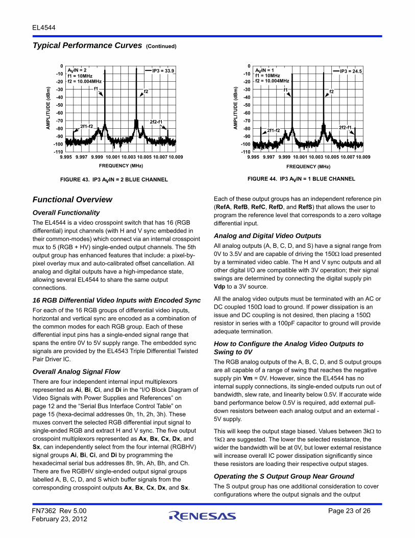
Operating the S Output Group Near Ground
The S output group has one additional consideration to cover configurations where the output signals and the output
FIGURE 43. IP3 AVIN = 2 BLUE CHANNEL FIGURE 44. IP3 AVIN = 1 BLUE CHANNEL
Typical Performance Curves (Continued)
-110
-100
-90
-80
-70
-60
-50
-40
-30
-20
-10
9.995 9.997 9.999 10.001 10.003 10.005 10.007 10.009
FREQUENCY (MHz)
AM
PL
ITU
DE
(d
Bm
)
IP3 = 33.9AVIN = 2f1 = 10MHzf2 = 10.004MHz
0
f1f2
2f2-f12f1-f2
-110
-100
-90
-80
-70
-60
-50
-40
-30
-20
-10
0
9.995 9.997 9.999 10.001 10.003 10.005 10.007 10.009
FREQUENCY (MHz)
AM
PL
ITU
DE
(d
Bm
)
IP3 = 24.5AVIN = 1f1 = 10MHzf2 = 10.004MHz
f2
2f1-f22f2-f1
f1
FN7362 Rev 5.00 Page 23 of 26February 23, 2012

EL4544
reference pin RefS are operated below 0.5V. Under these circumstances, each of the three auto-zero monitoring pins RAZ, GAZ, and BAZ, require an external 10k resistor connecting each to an external -5V supply. This keeps the auto-zero circuitry active all the way down to ground.
Switchable Video Output Group Has Overlay Capability and Offset Cancellation
The S group of output signals have an overlay switch that allows single-ended inputs ROL, GOL, and BOL, to be inserted on a pixel-by-pixel basis. The pin RefOL allows the user to program the overlay input (reference) level that produces an output voltage equal to the output reference pin RefS. The S group of video outputs has an Auto-Calibration mode which can null out offsets through the entire selected signal path from its inputs to its outputs. (It is usually triggered during the front or back porch of video when the input signal is known to be at Black Level).
Transparent vs Opaque Overlays
The overlay input for the S group is directly selected by the Overlay control pin Ovl. Two types of overlay are possible. The simplest overlay alternates between the dedicated overlay input and the "thru" input (that has been selected by the cross-point multiplexor). The "transparent" overlay mode is different from the standard overlay mode in that it presents the average of the overlay input and the "thru" input signal during overlay. The transparent mode is selected either by driving the Trans pin low or by programming bit D2 in Register D of the Serial Interface to a logical "1".
Serial Interface Control of the Auto-Calibration Feature
Programming bit D0 in Register D of the Serial Interface to a logical "1" activates the "Auto-Calibration" Mode which allows offsets from all inputs to the S group to be nulled-out via a calibration sequence. The programming Bit D1 in Register D of the Serial Interface is called Toggle. It allows for two modes of auto-calibration. If Toggle is programmed to a logical "0", Toggle mode is inactive. The auto-calibration cycle must be executed separately for both input groups (the overlay and the through signal groups).
What Happens During an Auto-Calibration Cycle
The auto-calibration (auto-zero) feature only applies to the S group of outputs. An auto-calibration cycle works as follows for either the overlay input or a selected "thru" input from the cross-point: During any time when the input signal is known to be at a "zero-level" ("zero-level" is a differential-zero input signal for any of the 16-RGB differential inputs or when the pin voltages to the overlay inputs ROL = GOL = BOL are all equal to RefOL), setting the calibration pin Cal to a logical "LO" activates the sample phase of auto-calibration and forces the analog outputs to be equal to the reference voltage of pin RefS. When pin Cal is brought back to a logical "HI", the calibration is held until the next calibration cycle, and the S group will accurately convey the video signal with low offsets. A
small hold-step (1mV) can be observed whenever the calibration signal is released. Each subsequent activation of the sampling phase refreshes the calibration. If Toggle mode is inactive, the user must individually calibrate both the overlay and non-overlay ("thru") output states by selecting the between them and running calibration separately for both of the input conditions. Changing the input selections by reprogramming the crosspoint to another input path or by changing the overlay mode (transparent/opaque), requires refreshing of this calibration. Ideally, the calibration is refreshed once per line of video. The drift during a line of video is negligible. (On the lab bench, using manual control, a drift rate on the order of 0.2mV/s will be observed.)
Toggle Mode Automatically Supervises the Calibration Cycles
The purpose of Toggle mode is to automatically alternate between calibrating the overlay and calibrating the "thru" paths to the S Output group. The Toggle mode assumes that overlays never exist outside of the video screen (that overlay only occurs during active video). When using the Toggle mode, the overlay function must be inactive during and around sync. When Toggle mode is active and the overlay switch is disabled, the EL4544 will automatically toggle between "thru" and overlay selections for alternate pulsing of the calibrate signal. Thus, every alternate calibrate pulse will override the selected "thru" state of the overlay switch, perform an auto-zero function, and then return the overlay switch back to its original "thru" position. This is true if the programming Bit D1 in Register D (labelled Toggle) of the Serial Interface is programmed to a logical "1". Whenever the IC is reset by momentarily pulling the Reset pin "LO", the Toggle mode is initialized such that the first path calibrated is the overlay path. The next calibration cycle will automatically calibrate the "thru" path.
Incorrect Use of the Toggle Mode
If the overlay is selected during auto-calibration with the Toggle mode active, the "thru" path will never be calibrated. Only the overlay gets calibrated in this configuration.
Integrated Die Temperature Probes
Thermal monitoring pins TMon1 and TMon2 allow the user to effectively monitor the die temperature by lightly forward biasing internal diodes and measuring their forward voltage drop. Since these diodes will have a -2mV/°C tempco, they can be an effective means of evaluating the thermal management of the user's application board and may even be configured to provide a thermally-triggered shutdown. To implement this feature, pull either of these pins below the negative supply with precision current source of 10µA to 100µA. Measure the forward drop at room temperature with the chip disabled. During operation, every +1°C rise in temperature will produce a 2mV drop in the forward voltage.
FN7362 Rev 5.00 Page 24 of 26February 23, 2012

EL4544
Intersil products are manufactured, assembled and tested utilizing ISO9001 quality systems as notedin the quality certifications found at www.intersil.com/en/support/qualandreliability.html
Intersil products are sold by description only. Intersil may modify the circuit design and/or specifications of products at any time without notice, provided that such modification does not, in Intersil's sole judgment, affect the form, fit or function of the product. Accordingly, the reader is cautioned to verify that datasheets are current before placing orders. Information furnished by Intersil is believed to be accurate and reliable. However, no responsibility is assumed by Intersil or its subsidiaries for its use; nor for any infringements of patents or other rights of third parties which may result from its use. No license is granted by implication or otherwise under any patent or patent rights of Intersil or its subsidiaries.
For information regarding Intersil Corporation and its products, see www.intersil.com
For additional products, see www.intersil.com/en/products.html
© Copyright Intersil Americas LLC 2005-2007. All Rights Reserved.All trademarks and registered trademarks are the property of their respective owners.
Some Tips on the Most Effective Programming of the EL4544
The video inputs present a 1.75k single ended and a 3.5k differential load to an incoming video signal. Since this load is in parallel with the external termination network, it has a consistent effect on the system gain. To maintain this consistency, it is inadvisable to program more than one input stage (Ai, Bi, Ci, or Di) to "look" at any given video input (RGB0, RGB1, …, RGBF) since each activated input stage puts an additional parallel load of 3.5k onto the selected input. When programming the serial interface this is simply expressed as: Avoid programming the same value into the four data registers (for Ai, Bi, Ci, and Di) at hex addresses 0H, 1H, 2H, and 3H. They should all have unique values. This is important since if any inputs are selected more than once, their gains will mismatch an input that has only been selected once.
If one wishes to broadcast the same signal to multiple output channels, this can easily be accomplished without violating the advice of the previous paragraph. Select the input that needs to be broadcast using any one of the four input selectors (Ai, Bi, Ci, or Di), then have any of up to five of the output stages (Ax, Bx, Cx, Dx, Sx) point to the input stage that is pointing to the desired input signal. These are selected using hex 8H, 9H, AH, BH, and CH. Now the EL4544 is broadcasting a single video source to multiple outputs without excessively loading down the selected input.
Sync Decoding of EL4544
The EL4544 is designed to receive and decode Horizontal and Vertical Sync signals that have been encoded as
common-mode signals of the Red, Green, and Blue Video inputs. The EL4543 provides this encoding as shown in Table 1.
The EL4544 decodes the common-mode signals into H and V syncs as follows: Horizontal Sync is TRUE when the Blue_Common_Mode voltage is greater than the Average_of_Red_and_Green_Common_Mode voltage. Vertical Sync is TRUE when the Average_of_Red_and_Blue_Common_Mode voltage is greater than the Green_Common_Mode voltage. The sync comparators have an internal symmetrical hysteresis that is less than ±50mV. Timing skews between comparators under all conditions are less than one pixel. The comparators have an input common mode that allows for operation at least 1V from the negative supplies and at least 1.5V from the positive supplies.
Logic Levels for Serial Interface and Control Logic
TABLE 1. SYNC SIGNAL ENCODING
H V
COMMON MODE A
(RED)
COMMON MODE B (GREEN)
COMMON MODE C (BLUE)
Low High 3.0 2.0 2.5
Low Low 2.5 3.0 2.0
High Low 2.0 3.0 2.5
High High 2.5 2.0 3.0
TABLE 2. INPUT LOGIC THRESHOLD (+5V SUPPLY)
VLO, max 0.8V
VHI, min 2V
FN7362 Rev 5.00 Page 25 of 26February 23, 2012

EL4544
FN7362 Rev 5.00 Page 26 of 26February 23, 2012
Package Outline Drawing
V356.27x27B356 BALL PLASTIC BALL GRID ARRAY PACKAGE (PBGA)Rev 2, 10/10
NON SOLDERMASK DEFINED PADS.
1.27
1.27
SOLDERMASK OPENING = 0.67MM (TYP x356) PAD DIAMATER = 0.55MM (TYP X356)
registered outline MS-034/A variation BAL-2.
A1 ball pad corner I.D. for plate mold: To be marked by ink.
Reference specifications: This drawing conforms to JEDEC
crowns of the solder balls.
Primary datum C and seating plane are defined by the spherical
All dimensions and tolerances conform to ASME Y14.5M-1994.
6.
3 .
5.
4.
1.
Dimensions are in millimeters.2.
NOTES:
BOTTOM VIEW
SIDE VIEWTYPICAL RECOMMENDED LAND PATTERN
TOP VIEW
B
4X 45°
A1 BALL PAD5.
A1 BALL
0.20 (4X)
A
0.56 ±0.06
1.17±0.05
0.60±0.10
2.33 ±0.21
SEATING PLANE4.
0.35 C
0.25 C
C
30° TYP
Ø0.30 M C A B
3.
0.15 C
24.00+0.35-0.05
4X 10.00 27.00
24.00+0.35-0.05
4X 10.00
27.00
0.76 +0.14-0.16
(1.44)
(1.44) 1.273X R0.50
YWVUTRPN
1.27
20 1417
1819
1615 1113
12 109
D
H
KLM
J
FG
E
78 6 4
5 3
BC
A
21
Ø16.8 AVAILABLE MARKING AREA
PAD CORNER
INDICATOR, 1.0DIA., OPTIONAL
CHAMFER
Ø0.15 M C
Dimension is measured at the maximum solder ball diameter, parallel to primary datum C.
Auto mold: Dimple to be formed by mold cap.