ISL9110A Datasheet - Renesas Electronics
16
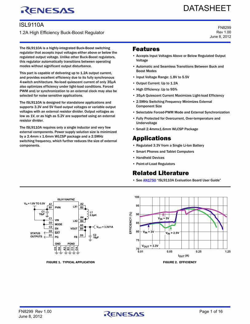
FN8299 Rev 1.00 Page 1 of 16 June 8, 2012 FN8299 Rev 1.00 June 8, 2012 ISL9110A 1.2A High Efficiency Buck-Boost Regulator DATASHEET The ISL9110A is a highly-integrated Buck-Boost switching regulator that accepts input voltages either above or below the regulated output voltage. Unlike other Buck-Boost regulators, this regulator automatically transitions between operating modes without significant output disturbance. This part is capable of delivering up to 1.2A output current, and provides excellent efficiency due to its fully synchronous 4-switch architecture. No-load quiescent current of only 35μA also optimizes efficiency under light-load conditions. Forced PWM and/or synchronization to an external clock may also be selected for noise sensitive applications. The ISL9110A is designed for standalone applications and supports 3.3V and 5V fixed output voltages or variable output voltages with an external resistor divider. Output voltages as low as 1V, or as high as 5.2V are supported using an external resistor divider. The ISL9110A requires only a single inductor and very few external components. Power supply solution size is minimized by a 2.4mm x 1.6mm WLCSP package and a 2.5MHz switching frequency, which further reduces the size of external components. Features • Accepts Input Voltages Above or Below Regulated Output Voltage • Automatic and Seamless Transitions Between Buck and Boost Modes • Input Voltage Range: 1.8V to 5.5V • Output Current: Up to 1.2A • High Efficiency: Up to 95% • 35μA Quiescent Current Maximizes Light-load Efficiency • 2.5MHz Switching Frequency Minimizes External Component Size • Selectable Forced-PWM Mode and External Synchronization • Fully Protected for Overcurrent, Over-temperature and Undervoltage • Small 2.4mmx1.6mm WLCSP Package Applications • Regulated 3.3V from a Single Li-Ion Battery • Smart Phones and Tablet Computers • Handheld Devices • Point-of-Load Regulators Related Literature • See AN1750 “ISL9110A Evaluation Board User Guide” FIGURE 1. TYPICAL APPLICATION FIGURE 2. EFFICIENCY VOUT = 3.3V/1A VOUT A5 FB D5 C2 10µF BAT PG STATUS OUTPUTS D2 D1 PVIN VIN = 1.8V TO 5.5V VIN B1 C1 MODE EN D3 C2 C1 10µF ISL9110AIITNZ D4 C3 LX1 LX2 B2 A4 L1 2.2µH B5 GND C5 B3 A3 C4 PGND B4 A2 A1 I OUT (A) EFFICIENCY (%) 70 75 80 85 90 95 100 0.01 0.05 0.25 1.25 V IN = 5V V IN = 2.5V V IN = 3V V OUT = 3.3V
Transcript of ISL9110A Datasheet - Renesas Electronics
FN8299Rev 1.00
June 8, 2012
ISL9110A1.2A High Efficiency Buck-Boost Regulator
DATASHEET
The ISL9110A is a highly-integrated Buck-Boost switching regulator that accepts input voltages either above or below the regulated output voltage. Unlike other Buck-Boost regulators, this regulator automatically transitions between operating modes without significant output disturbance.
This part is capable of delivering up to 1.2A output current, and provides excellent efficiency due to its fully synchronous 4-switch architecture. No-load quiescent current of only 35µA also optimizes efficiency under light-load conditions. Forced PWM and/or synchronization to an external clock may also be selected for noise sensitive applications.
The ISL9110A is designed for standalone applications and supports 3.3V and 5V fixed output voltages or variable output voltages with an external resistor divider. Output voltages as low as 1V, or as high as 5.2V are supported using an external resistor divider.
The ISL9110A requires only a single inductor and very few external components. Power supply solution size is minimized by a 2.4mm x 1.6mm WLCSP package and a 2.5MHz switching frequency, which further reduces the size of external components.
Features• Accepts Input Voltages Above or Below Regulated Output
Voltage
• Automatic and Seamless Transitions Between Buck and Boost Modes
• Input Voltage Range: 1.8V to 5.5V
• Output Current: Up to 1.2A
• High Efficiency: Up to 95%
• 35µA Quiescent Current Maximizes Light-load Efficiency
• 2.5MHz Switching Frequency Minimizes External Component Size
• Selectable Forced-PWM Mode and External Synchronization
• Fully Protected for Overcurrent, Over-temperature and Undervoltage
• Small 2.4mmx1.6mm WLCSP Package
Applications• Regulated 3.3V from a Single Li-Ion Battery
• Smart Phones and Tablet Computers
• Handheld Devices
• Point-of-Load Regulators
Related Literature• See AN1750 “ISL9110A Evaluation Board User Guide”
FIGURE 1. TYPICAL APPLICATION FIGURE 2. EFFICIENCY
VOUT = 3.3V/1AVOUT
A5
FBD5 C2
10µF
BAT
PG
STATUSOUTPUTS
D2
D1
PVIN
VIN = 1.8V TO 5.5V
VIN
B1
C1
MODE
EN
D3
C2
C110µF
ISL9110AIITNZ
D4
C3
LX1
LX2
B2
A4
L12.2µH
B5
GND
C5
B3
A3
C4
PGND
B4
A2A1
IOUT (A)
EF
FIC
IEN
CY
(%
)
70
75
80
85
90
95
100
0.01 0.05 0.25 1.25
VIN = 5V
VIN = 2.5VVIN = 3V
VOUT = 3.3V
FN8299 Rev 1.00 Page 1 of 16June 8, 2012
ISL9110A
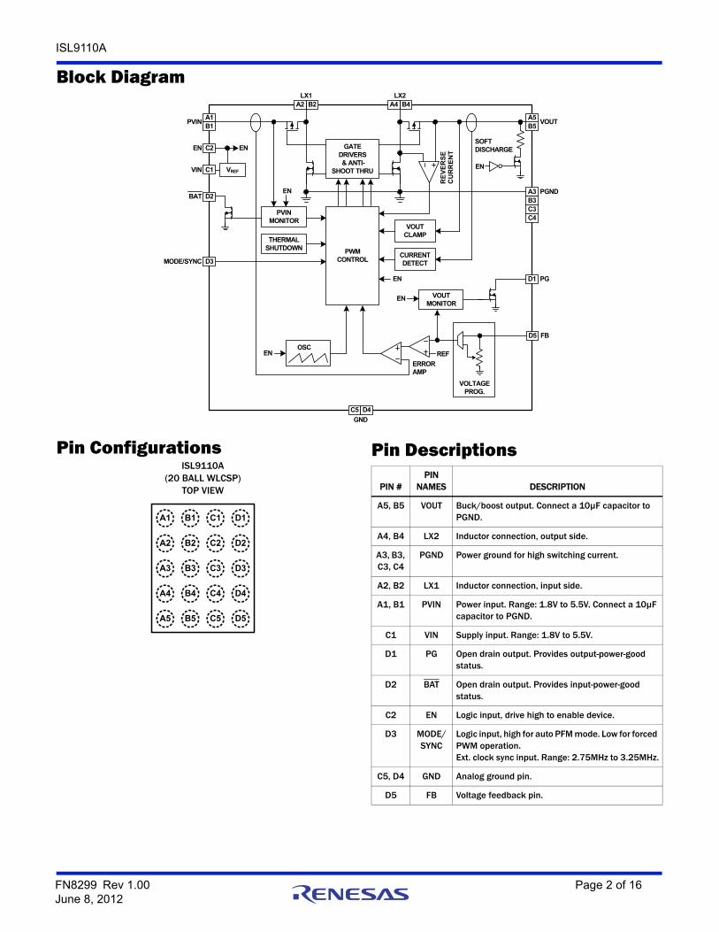
Block Diagram
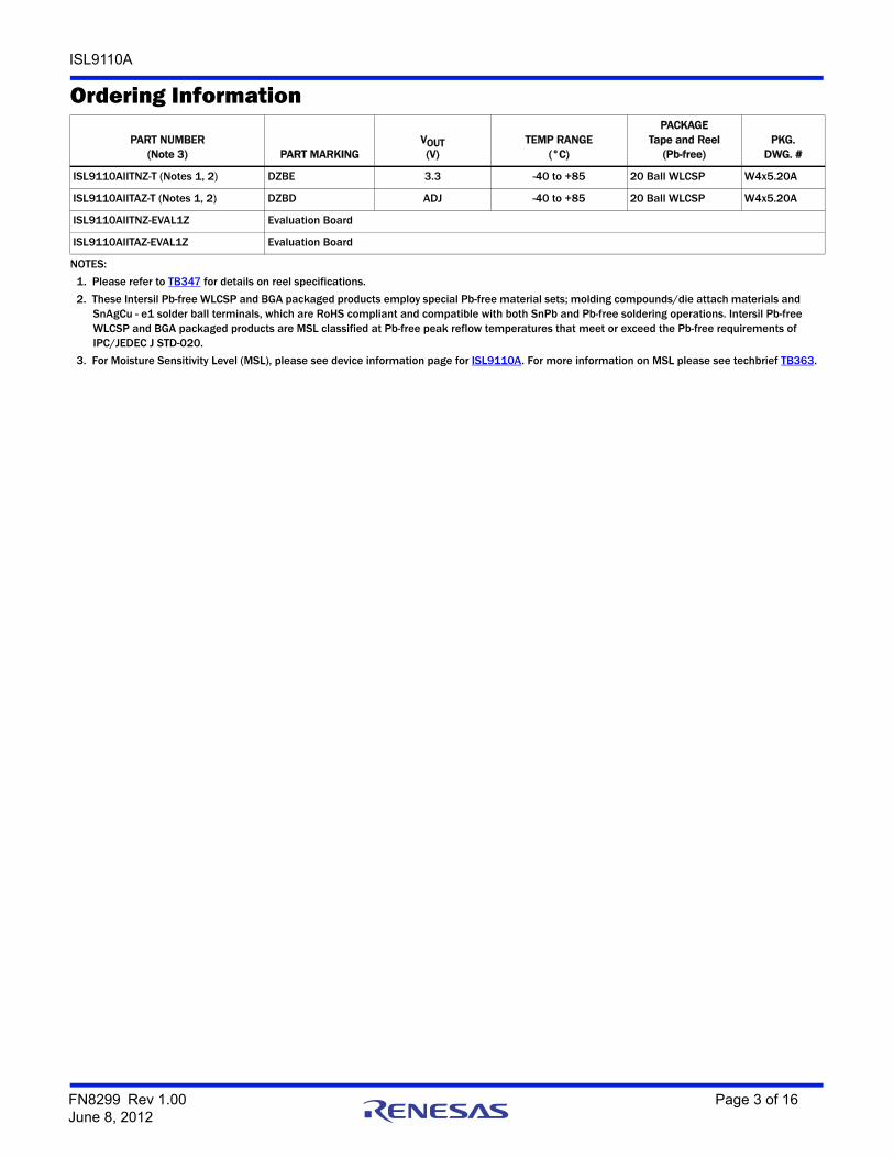
Pin ConfigurationsISL9110A
(20 BALL WLCSP)TOP VIEW
OSC
ERROR AMP
PVIN
PWM CONTROL
PVIN MONITOR
LX1
VREF
REF
RE
VE
RS
E
CU
RR
EN
T
VOUTA1
B2 B4LX2
GATE DRIVERS & ANTI-
SHOOT THRUC1VIN
THERMALSHUTDOWN
CURRENTDETECT
B5
VOUTMONITOR
C2
EN
D5 FB
A3 PGND
C5
GND
EN
EN
EN
EN EN
VOUTCLAMP
D2BAT
D3MODE/SYNC
D1 PG
VOLTAGEPROG.
EN
SOFTDISCHARGE
A5
A4A2
B1
B3C3C4
D4
A1 B1
A2 B2
C1 D1
C2 D2
A3 B3
A4 B4
C3 D3
C4 D4
A5 B5 C5 D5
Pin Descriptions
PIN #PIN
NAMES DESCRIPTION
A5, B5 VOUT Buck/boost output. Connect a 10µF capacitor to PGND.
A4, B4 LX2 Inductor connection, output side.
A3, B3, C3, C4
PGND Power ground for high switching current.
A2, B2 LX1 Inductor connection, input side.
A1, B1 PVIN Power input. Range: 1.8V to 5.5V. Connect a 10µF capacitor to PGND.
C1 VIN Supply input. Range: 1.8V to 5.5V.
D1 PG Open drain output. Provides output-power-good status.
D2 BAT Open drain output. Provides input-power-good status.
C2 EN Logic input, drive high to enable device.
D3 MODE/ SYNC
Logic input, high for auto PFM mode. Low for forced PWM operation.Ext. clock sync input. Range: 2.75MHz to 3.25MHz.
C5, D4 GND Analog ground pin.
D5 FB Voltage feedback pin.
FN8299 Rev 1.00 Page 2 of 16June 8, 2012
ISL9110A
Ordering Information
PART NUMBER(Note 3) PART MARKING
VOUT(V)
TEMP RANGE(°C)
PACKAGETape and Reel
(Pb-free)PKG.
DWG. #
ISL9110AIITNZ-T (Notes 1, 2) DZBE 3.3 -40 to +85 20 Ball WLCSP W4x5.20A
ISL9110AIITAZ-T (Notes 1, 2) DZBD ADJ -40 to +85 20 Ball WLCSP W4x5.20A
ISL9110AIITNZ-EVAL1Z Evaluation Board
ISL9110AIITAZ-EVAL1Z Evaluation Board
NOTES:
1. Please refer to TB347 for details on reel specifications.
2. These Intersil Pb-free WLCSP and BGA packaged products employ special Pb-free material sets; molding compounds/die attach materials and SnAgCu - e1 solder ball terminals, which are RoHS compliant and compatible with both SnPb and Pb-free soldering operations. Intersil Pb-free WLCSP and BGA packaged products are MSL classified at Pb-free peak reflow temperatures that meet or exceed the Pb-free requirements of IPC/JEDEC J STD-020.
3. For Moisture Sensitivity Level (MSL), please see device information page for ISL9110A. For more information on MSL please see techbrief TB363.
FN8299 Rev 1.00 Page 3 of 16June 8, 2012
ISL9110A
Table of ContentsApplications . . . . . . . . . . . . . . . . . . . . . . . . . . . . . . . . . . . . . . . . . . . . . . . . . . . . . . . . . . . . . . . . . . . . . . . . . . . . . . . . . . . . . . . . . . . . . . . . . . . . . . . . 1
Related Literature . . . . . . . . . . . . . . . . . . . . . . . . . . . . . . . . . . . . . . . . . . . . . . . . . . . . . . . . . . . . . . . . . . . . . . . . . . . . . . . . . . . . . . . . . . . . . . . . . . . 1
Block Diagram . . . . . . . . . . . . . . . . . . . . . . . . . . . . . . . . . . . . . . . . . . . . . . . . . . . . . . . . . . . . . . . . . . . . . . . . . . . . . . . . . . . . . . . . . . . . . . . . . . . . . . 2
Pin Descriptions. . . . . . . . . . . . . . . . . . . . . . . . . . . . . . . . . . . . . . . . . . . . . . . . . . . . . . . . . . . . . . . . . . . . . . . . . . . . . . . . . . . . . . . . . . . . . . . . . . . . . 2
Absolute Maximum Ratings. . . . . . . . . . . . . . . . . . . . . . . . . . . . . . . . . . . . . . . . . . . . . . . . . . . . . . . . . . . . . . . . . . . . . . . . . . . . . . . . . . . . . . . . . . . 5
Thermal Information . . . . . . . . . . . . . . . . . . . . . . . . . . . . . . . . . . . . . . . . . . . . . . . . . . . . . . . . . . . . . . . . . . . . . . . . . . . . . . . . . . . . . . . . . . . . . . . . . 5
Recommended Operating Conditions. . . . . . . . . . . . . . . . . . . . . . . . . . . . . . . . . . . . . . . . . . . . . . . . . . . . . . . . . . . . . . . . . . . . . . . . . . . . . . . . . . . 5
Analog Specifications . . . . . . . . . . . . . . . . . . . . . . . . . . . . . . . . . . . . . . . . . . . . . . . . . . . . . . . . . . . . . . . . . . . . . . . . . . . . . . . . . . . . . . . . . . . . . . . 5
Typical Performance Curves. . . . . . . . . . . . . . . . . . . . . . . . . . . . . . . . . . . . . . . . . . . . . . . . . . . . . . . . . . . . . . . . . . . . . . . . . . . . . . . . . . . . . . . . . . . 7
Functional Description . . . . . . . . . . . . . . . . . . . . . . . . . . . . . . . . . . . . . . . . . . . . . . . . . . . . . . . . . . . . . . . . . . . . . . . . . . . . . . . . . . . . . . . . . . . . . . 11Functional Overview . . . . . . . . . . . . . . . . . . . . . . . . . . . . . . . . . . . . . . . . . . . . . . . . . . . . . . . . . . . . . . . . . . . . . . . . . . . . . . . . . . . . . . . . . . . . . 11Internal Supply and References. . . . . . . . . . . . . . . . . . . . . . . . . . . . . . . . . . . . . . . . . . . . . . . . . . . . . . . . . . . . . . . . . . . . . . . . . . . . . . . . . . . . 11Enable Input . . . . . . . . . . . . . . . . . . . . . . . . . . . . . . . . . . . . . . . . . . . . . . . . . . . . . . . . . . . . . . . . . . . . . . . . . . . . . . . . . . . . . . . . . . . . . . . . . . . . 11Soft Discharge . . . . . . . . . . . . . . . . . . . . . . . . . . . . . . . . . . . . . . . . . . . . . . . . . . . . . . . . . . . . . . . . . . . . . . . . . . . . . . . . . . . . . . . . . . . . . . . . . . 11POR Sequence and Soft-start. . . . . . . . . . . . . . . . . . . . . . . . . . . . . . . . . . . . . . . . . . . . . . . . . . . . . . . . . . . . . . . . . . . . . . . . . . . . . . . . . . . . . . 11Overcurrent Protection . . . . . . . . . . . . . . . . . . . . . . . . . . . . . . . . . . . . . . . . . . . . . . . . . . . . . . . . . . . . . . . . . . . . . . . . . . . . . . . . . . . . . . . . . . . 11Short Circuit Protection. . . . . . . . . . . . . . . . . . . . . . . . . . . . . . . . . . . . . . . . . . . . . . . . . . . . . . . . . . . . . . . . . . . . . . . . . . . . . . . . . . . . . . . . . . . 11Undervoltage Lockout . . . . . . . . . . . . . . . . . . . . . . . . . . . . . . . . . . . . . . . . . . . . . . . . . . . . . . . . . . . . . . . . . . . . . . . . . . . . . . . . . . . . . . . . . . . . 11PG Status Output . . . . . . . . . . . . . . . . . . . . . . . . . . . . . . . . . . . . . . . . . . . . . . . . . . . . . . . . . . . . . . . . . . . . . . . . . . . . . . . . . . . . . . . . . . . . . . . . 11BAT Status Output . . . . . . . . . . . . . . . . . . . . . . . . . . . . . . . . . . . . . . . . . . . . . . . . . . . . . . . . . . . . . . . . . . . . . . . . . . . . . . . . . . . . . . . . . . . . . . . 11Ultrasonic Mode (Available Upon Request) . . . . . . . . . . . . . . . . . . . . . . . . . . . . . . . . . . . . . . . . . . . . . . . . . . . . . . . . . . . . . . . . . . . . . . . . . . 11Thermal Shutdown . . . . . . . . . . . . . . . . . . . . . . . . . . . . . . . . . . . . . . . . . . . . . . . . . . . . . . . . . . . . . . . . . . . . . . . . . . . . . . . . . . . . . . . . . . . . . . 12External Synchronization . . . . . . . . . . . . . . . . . . . . . . . . . . . . . . . . . . . . . . . . . . . . . . . . . . . . . . . . . . . . . . . . . . . . . . . . . . . . . . . . . . . . . . . . . 12Buck-Boost Conversion Topology. . . . . . . . . . . . . . . . . . . . . . . . . . . . . . . . . . . . . . . . . . . . . . . . . . . . . . . . . . . . . . . . . . . . . . . . . . . . . . . . . . . 12PWM Operation . . . . . . . . . . . . . . . . . . . . . . . . . . . . . . . . . . . . . . . . . . . . . . . . . . . . . . . . . . . . . . . . . . . . . . . . . . . . . . . . . . . . . . . . . . . . . . . . . 12PFM Operation . . . . . . . . . . . . . . . . . . . . . . . . . . . . . . . . . . . . . . . . . . . . . . . . . . . . . . . . . . . . . . . . . . . . . . . . . . . . . . . . . . . . . . . . . . . . . . . . . . 12Operation With VIN Close to VOUT. . . . . . . . . . . . . . . . . . . . . . . . . . . . . . . . . . . . . . . . . . . . . . . . . . . . . . . . . . . . . . . . . . . . . . . . . . . . . . . . . . 12Output Voltage Programming . . . . . . . . . . . . . . . . . . . . . . . . . . . . . . . . . . . . . . . . . . . . . . . . . . . . . . . . . . . . . . . . . . . . . . . . . . . . . . . . . . . . . 12
Applications Information . . . . . . . . . . . . . . . . . . . . . . . . . . . . . . . . . . . . . . . . . . . . . . . . . . . . . . . . . . . . . . . . . . . . . . . . . . . . . . . . . . . . . . . . . . . . 12Component Selection . . . . . . . . . . . . . . . . . . . . . . . . . . . . . . . . . . . . . . . . . . . . . . . . . . . . . . . . . . . . . . . . . . . . . . . . . . . . . . . . . . . . . . . . . . . . 12Output Voltage Programming, Adj. Version . . . . . . . . . . . . . . . . . . . . . . . . . . . . . . . . . . . . . . . . . . . . . . . . . . . . . . . . . . . . . . . . . . . . . . . . . . 13Feed-Forward Capacitor Selection. . . . . . . . . . . . . . . . . . . . . . . . . . . . . . . . . . . . . . . . . . . . . . . . . . . . . . . . . . . . . . . . . . . . . . . . . . . . . . . . . . 13Non-Adjustable Version FB Pin Connection . . . . . . . . . . . . . . . . . . . . . . . . . . . . . . . . . . . . . . . . . . . . . . . . . . . . . . . . . . . . . . . . . . . . . . . . . . 13Inductor Selection . . . . . . . . . . . . . . . . . . . . . . . . . . . . . . . . . . . . . . . . . . . . . . . . . . . . . . . . . . . . . . . . . . . . . . . . . . . . . . . . . . . . . . . . . . . . . . . 13PVIN and VOUT Capacitor Selection . . . . . . . . . . . . . . . . . . . . . . . . . . . . . . . . . . . . . . . . . . . . . . . . . . . . . . . . . . . . . . . . . . . . . . . . . . . . . . . . 13Application Example 1 . . . . . . . . . . . . . . . . . . . . . . . . . . . . . . . . . . . . . . . . . . . . . . . . . . . . . . . . . . . . . . . . . . . . . . . . . . . . . . . . . . . . . . . . . . . 13Application Example 2 . . . . . . . . . . . . . . . . . . . . . . . . . . . . . . . . . . . . . . . . . . . . . . . . . . . . . . . . . . . . . . . . . . . . . . . . . . . . . . . . . . . . . . . . . . . 13Recommended PCB Layout . . . . . . . . . . . . . . . . . . . . . . . . . . . . . . . . . . . . . . . . . . . . . . . . . . . . . . . . . . . . . . . . . . . . . . . . . . . . . . . . . . . . . . . 13
Revision History . . . . . . . . . . . . . . . . . . . . . . . . . . . . . . . . . . . . . . . . . . . . . . . . . . . . . . . . . . . . . . . . . . . . . . . . . . . . . . . . . . . . . . . . . . . . . . . . . . . . 15
Products . . . . . . . . . . . . . . . . . . . . . . . . . . . . . . . . . . . . . . . . . . . . . . . . . . . . . . . . . . . . . . . . . . . . . . . . . . . . . . . . . . . . . . . . . . . . . . . . . . . . . . . . . . 15
Package Outline Drawing. . . . . . . . . . . . . . . . . . . . . . . . . . . . . . . . . . . . . . . . . . . . . . . . . . . . . . . . . . . . . . . . . . . . . . . . . . . . . . . . . . . . . . . . . . . 16
FN8299 Rev 1.00 Page 4 of 16June 8, 2012
ISL9110A
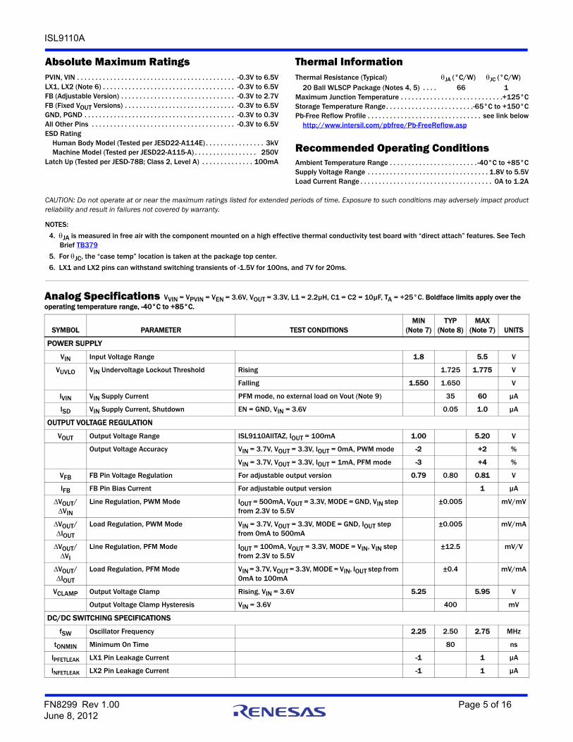
Absolute Maximum Ratings Thermal InformationPVIN, VIN . . . . . . . . . . . . . . . . . . . . . . . . . . . . . . . . . . . . . . . . . . . -0.3V to 6.5VLX1, LX2 (Note 6) . . . . . . . . . . . . . . . . . . . . . . . . . . . . . . . . . . . . -0.3V to 6.5VFB (Adjustable Version) . . . . . . . . . . . . . . . . . . . . . . . . . . . . . . . -0.3V to 2.7VFB (Fixed VOUT Versions) . . . . . . . . . . . . . . . . . . . . . . . . . . . . . . -0.3V to 6.5VGND, PGND . . . . . . . . . . . . . . . . . . . . . . . . . . . . . . . . . . . . . . . . . -0.3V to 0.3VAll Other Pins . . . . . . . . . . . . . . . . . . . . . . . . . . . . . . . . . . . . . . . -0.3V to 6.5VESD Rating
Human Body Model (Tested per JESD22-A114E) . . . . . . . . . . . . . . . . 3kVMachine Model (Tested per JESD22-A115-A) . . . . . . . . . . . . . . . . . 250V
Latch Up (Tested per JESD-78B; Class 2, Level A) . . . . . . . . . . . . . . 100mA
Thermal Resistance (Typical) JA (°C/W) JC (°C/W)20 Ball WLSCP Package (Notes 4, 5) . . . . 66 1
Maximum Junction Temperature . . . . . . . . . . . . . . . . . . . . . . . . . . . .+125°CStorage Temperature Range. . . . . . . . . . . . . . . . . . . . . . . .-65°C to +150°CPb-Free Reflow Profile . . . . . . . . . . . . . . . . . . . . . . . . . . . . . . . see link below
http://www.intersil.com/pbfree/Pb-FreeReflow.asp
Recommended Operating ConditionsAmbient Temperature Range . . . . . . . . . . . . . . . . . . . . . . . . -40°C to +85°CSupply Voltage Range . . . . . . . . . . . . . . . . . . . . . . . . . . . . . . . . . 1.8V to 5.5VLoad Current Range . . . . . . . . . . . . . . . . . . . . . . . . . . . . . . . . . . . . 0A to 1.2A
CAUTION: Do not operate at or near the maximum ratings listed for extended periods of time. Exposure to such conditions may adversely impact productreliability and result in failures not covered by warranty.
NOTES:
4. JA is measured in free air with the component mounted on a high effective thermal conductivity test board with “direct attach” features. See Tech Brief TB379
5. For JC, the “case temp” location is taken at the package top center.
6. LX1 and LX2 pins can withstand switching transients of -1.5V for 100ns, and 7V for 20ms.
Analog Specifications VVIN = VPVIN = VEN = 3.6V, VOUT = 3.3V, L1 = 2.2µH, C1 = C2 = 10µF, TA = +25°C. Boldface limits apply over the operating temperature range, -40°C to +85°C.
SYMBOL PARAMETER TEST CONDITIONSMIN
(Note 7)TYP
(Note 8)MAX
(Note 7) UNITS
POWER SUPPLY
VIN Input Voltage Range 1.8 5.5 V
VUVLO VIN Undervoltage Lockout Threshold Rising 1.725 1.775 V
Falling 1.550 1.650 V
IVIN VIN Supply Current PFM mode, no external load on Vout (Note 9) 35 60 µA
ISD VIN Supply Current, Shutdown EN = GND, VIN = 3.6V 0.05 1.0 µA
OUTPUT VOLTAGE REGULATION
VOUT Output Voltage Range ISL9110AIITAZ, IOUT = 100mA 1.00 5.20 V
Output Voltage Accuracy VIN = 3.7V, VOUT = 3.3V, IOUT = 0mA, PWM mode -2 +2 %
VIN = 3.7V, VOUT = 3.3V, IOUT = 1mA, PFM mode -3 +4 %
VFB FB Pin Voltage Regulation For adjustable output version 0.79 0.80 0.81 V
IFB FB Pin Bias Current For adjustable output version 1 µA
VOUT/VIN
Line Regulation, PWM Mode IOUT = 500mA, VOUT = 3.3V, MODE = GND, VIN step from 2.3V to 5.5V
±0.005 mV/mV
VOUT/IOUT
Load Regulation, PWM Mode VIN = 3.7V, VOUT = 3.3V, MODE = GND, IOUT step from 0mA to 500mA
±0.005 mV/mA
VOUT/VI
Line Regulation, PFM Mode IOUT = 100mA, VOUT = 3.3V, MODE = VIN, VIN step from 2.3V to 5.5V
±12.5 mV/V
VOUT/IOUT
Load Regulation, PFM Mode VIN = 3.7V, VOUT = 3.3V, MODE = VIN, IOUT step from 0mA to 100mA
±0.4 mV/mA
VCLAMP Output Voltage Clamp Rising, VIN = 3.6V 5.25 5.95 V
Output Voltage Clamp Hysteresis VIN = 3.6V 400 mV
DC/DC SWITCHING SPECIFICATIONS
fSW Oscillator Frequency 2.25 2.50 2.75 MHz
tONMIN Minimum On Time 80 ns
IPFETLEAK LX1 Pin Leakage Current -1 1 µA
INFETLEAK LX2 Pin Leakage Current -1 1 µA
FN8299 Rev 1.00 Page 5 of 16June 8, 2012
ISL9110A
SOFT-START and SOFT DISCHARGE
tSS Soft-start Time Time from when EN signal asserts to when output voltage ramp starts.
1 ms
Time from when output voltage ramp starts to when output voltage reaches 95% of its nominal value with device operating in buck mode.VIN = 4V, VOUT = 3.3V, IO = 200mA
1 ms
Time from when output voltage ramp starts to when output voltage reaches 95% of its nominal value with device operating in boost mode.VIN = 2V, VOUT = 3.3V, IO = 200mA
2 ms
RDISCHG VOUT Soft-Discharge ON-Resistance VIN = 3.6V, EN < VIL 120
POWER MOSFET
RDSON_P P-Channel MOSFET ON-Resistance VIN = 3.6V, IO = 200mA 0.10 0.17
VIN = 2.5V, IO = 200mA 0.13 0.23
RDSON_N N-Channel MOSFET ON-Resistance VIN = 3.6V, IO = 200mA 0.09 0.15
VIN = 2.5V, IO = 200mA 0.11 0.23
IPK_LMT P-Channel MOSFET Peak Current Limit VIN = 3.6V 2.0 2.4 2.8 A
PFM/PWM TRANSITION
Load Current Threshold, PFM to PWM VIN = 3.6V, VOUT = 3.3V 200 mA
Load Current Threshold, PWM to PFM VIN = 3.6V, VOUT = 3.3V 75 mA
External Synchronization Frequency Range 2.75 3.25 MHz
Thermal Shutdown 155 °C
Thermal Shutdown Hysteresis 30 °C
BATTERY MONITOR AND POWER GOOD COMPARATORS
VTBMON Battery Monitor Voltage Threshold 1.85 2.0 2.15 V
VHBMON Battery Monitor Voltage Hysteresis 100 mV
tBMON Battery Monitor Debounce Time 25 µs
PG Delay Time (Rising) 1 ms
PG Delay Time (Falling) 20 µs
Minimum Supply Voltage for Valid PG Signal EN = VIN 1.2 V
PGRNGLR PG Range - Lower (Rising) Percentage of programmed voltage 90 %
PGRNGLF PG Range - Lower (Falling) Percentage of programmed voltage 87 %
PGRNGUR PG Range - Upper (Rising) Percentage of programmed voltage 112 %
PGRNGUF PG Range - Upper (Falling) Percentage of programmed voltage 110 %
Compliance Voltage - PG, BAT VIN = 3.6V, ISINK = 1mA 0.3 V
LOGIC INPUTS
ILEAK Input Leakage 0.05 1 µA
VIH Input HIGH Voltage 1.4 V
VIL Input LOW Voltage 0.4 V
NOTES:
7. Parameters with MIN and/or MAX limits are 100% tested at +25°C, unless otherwise specified. Temperature limits established by characterization and are not production tested.
8. Typical values are for TA = +25°C and VIN = 3.6V.
9. Quiescent current measurements are taken when the output is not switching.
Analog Specifications VVIN = VPVIN = VEN = 3.6V, VOUT = 3.3V, L1 = 2.2µH, C1 = C2 = 10µF, TA = +25°C. Boldface limits apply over the operating temperature range, -40°C to +85°C. (Continued)
SYMBOL PARAMETER TEST CONDITIONSMIN
(Note 7)TYP
(Note 8)MAX
(Note 7) UNITS
FN8299 Rev 1.00 Page 6 of 16June 8, 2012
ISL9110A
Typical Performance Curves
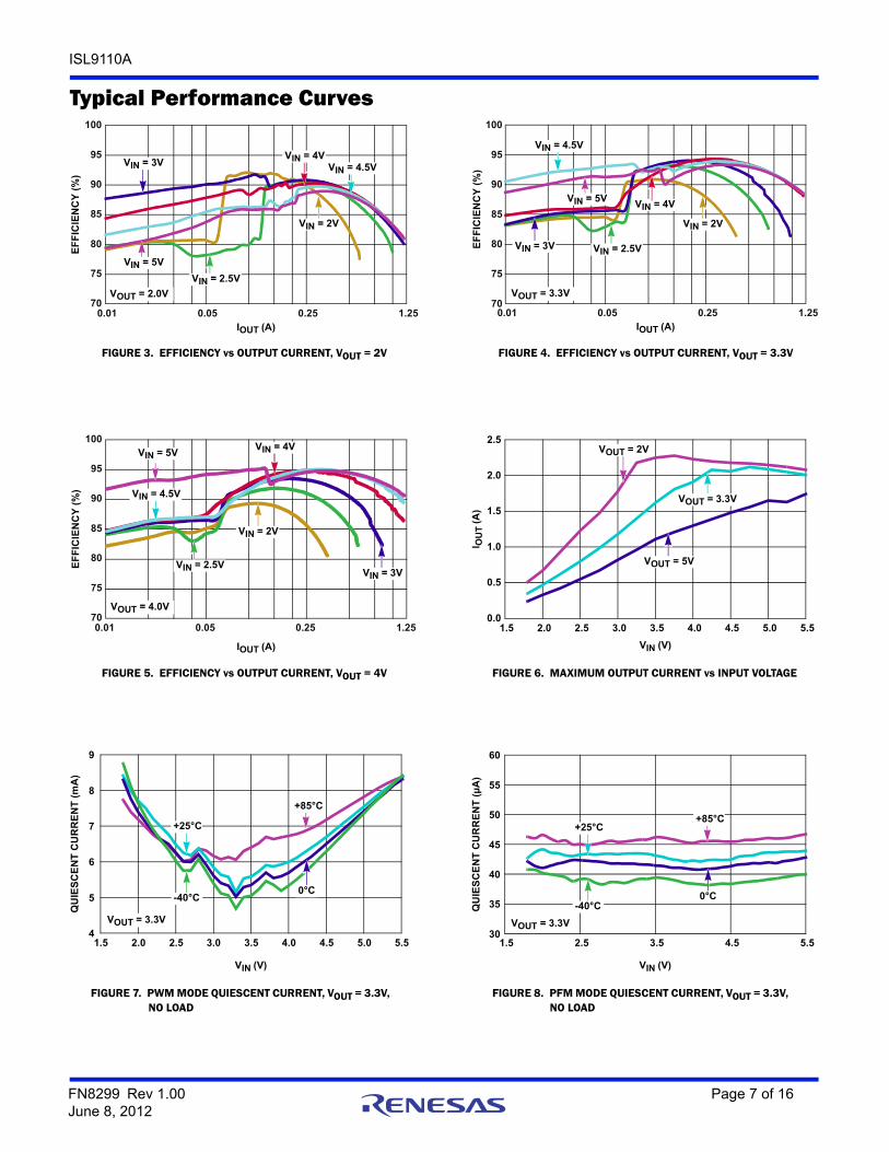
FIGURE 3. EFFICIENCY vs OUTPUT CURRENT, VOUT = 2V FIGURE 4. EFFICIENCY vs OUTPUT CURRENT, VOUT = 3.3V
FIGURE 5. EFFICIENCY vs OUTPUT CURRENT, VOUT = 4V FIGURE 6. MAXIMUM OUTPUT CURRENT vs INPUT VOLTAGE
FIGURE 7. PWM MODE QUIESCENT CURRENT, VOUT = 3.3V, NO LOAD
FIGURE 8. PFM MODE QUIESCENT CURRENT, VOUT = 3.3V, NO LOAD
70
75
80
85
90
95
100
0.01 0.05 0.25 1.25IOUT (A)
EF
FIC
IEN
CY
(%
)
VIN = 5V
VIN = 4.5V
VIN = 2.5V
VIN = 3V
VIN = 2V
VOUT = 2.0V
VIN = 4V
IOUT (A)
EF
FIC
IEN
CY
(%
)
70
75
80
85
90
95
100
0.01 0.05 0.25 1.25
VIN = 5V
VIN = 4.5V
VIN = 4V
VIN = 2.5V
VIN = 2V
VOUT = 3.3V
VIN = 3V
70
75
80
85
90
95
100
0.01 0.05 0.25 1.25
IOUT (A)
EF
FIC
IEN
CY
(%
)
VIN = 5V
VIN = 4.5V
VIN = 2.5VVIN = 3V
VIN = 2V
VOUT = 4.0V
VIN = 4V
0.0
0.5
1.0
1.5
2.0
2.5
1.5 2.0 2.5 3.0 3.5 4.0 4.5 5.0 5.5
I OU
T (
A)
VIN (V)
VOUT = 5V
VOUT = 3.3V
VOUT = 2V
4
5
6
7
8
9
1.5 2.0 2.5 3.0 3.5 4.0 4.5 5.0 5.5
QU
IES
CE
NT
CU
RR
EN
T (
mA
)
VIN (V)
-40°C0°C
+25°C
+85°C
VOUT = 3.3V
30
35
40
45
50
55
60
1.5 2.5 3.5 4.5 5.5
-40°C0°C
+25°C+85°C
VOUT = 3.3V
QU
IES
CE
NT
CU
RR
EN
T (
µA
)
VIN (V)
FN8299 Rev 1.00 Page 7 of 16June 8, 2012
ISL9110A
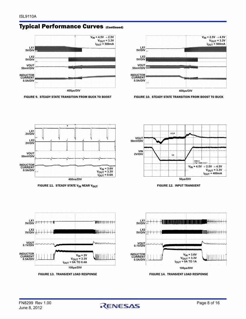
FIGURE 9. STEADY STATE TRANSITION FROM BUCK TO BOOST FIGURE 10. STEADY STATE TRANSITION FROM BOOST TO BUCK
FIGURE 11. STEADY STATE VIN NEAR VOUT FIGURE 12. INPUT TRANSIENT
FIGURE 13. TRANSIENT LOAD RESPONSE FIGURE 14. TRANSIENT LOAD RESPONSE
Typical Performance Curves (Continued)
LX15V/DIV
5V/DIVLX2
50mV/DIVVOUT
0.5A/DIVCURRENT
INDUCTOR
400µs/DIV
VIN = 4.5V 2.5VVOUT = 3.3V
IOUT = 500mALX1
5V/DIV
5V/DIVLX2
50mV/DIVVOUT
0.5A/DIVCURRENT
INDUCTOR
400µs/DIV
VIN = 2.5V 4.5VVOUT = 3.3V
IOUT = 500mA
LX12V/DIV
2V/DIVLX2
50mV/DIVVOUT
0.5A/DIVCURRENT
INDUCTOR
400ns/DIV
VIN = 3.6VVOUT = 3.3VIOUT = 0.6A
50mV/DIVVOUT
2V/DIVVIN
50µs/DIV
VIN = 4.5V 2.5V 4.5VVOUT = 3.3V
IOUT = 400mA
0.1V/DIVVOUT
0.5A/DIVCURRENT
INDUCTOR
100µs/DIV
LX15V/DIV
5V/DIVLX2
VIN = 2VVOUT = 3.3V
IOUT = 0A TO 0.4A
LX15V/DIV
5V/DIVLX2
0.1V/DIVVOUT
0.5A/DIVCURRENT
INDUCTOR
100µs/DIV
VIN = 3.6VVOUT = 3.3V
IOUT = 0A TO 1A
FN8299 Rev 1.00 Page 8 of 16June 8, 2012
ISL9110A
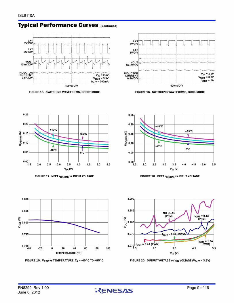
FIGURE 15. SWITCHING WAVEFORMS, BOOST MODE FIGURE 16. SWITCHING WAVEFORMS, BUCK MODE
FIGURE 17. NFET rDS(ON) vs INPUT VOLTAGE FIGURE 18. PFET rDS(ON) vs INPUT VOLTAGE
FIGURE 19. VREF vs TEMPERATURE, TA = -40°C TO +85°C FIGURE 20. OUTPUT VOLTAGE vs VIN VOLTAGE (VOUT = 3.3V)
Typical Performance Curves (Continued)
LX12V/DIV
2V/DIVLX2
10mV/DIVVOUT
0.5A/DIVCURRENT
INDUCTOR
400ns/DIV
VIN = 2.5VVOUT = 3.3V
IOUT = 500mA
LX15V/DIV
5V/DIVLX2
10mV/DIVVOUT
0.5A/DIVCURRENT
INDUCTOR
400ns/DIV
VIN = 4.5VVOUT = 3.3V
IOUT = 1A
0.00
0.05
0.10
0.15
0.20
0.25
1.5 2.0 2.5 3.0 3.5 4.0 4.5 5.0 5.5
-40°C0°C
+40°C
+85°C
RD
S(O
N)
(Ω)
VIN (V)
0.00
0.05
0.10
0.15
0.20
0.25
1.5 2.0 2.5 3.0 3.5 4.0 4.5 5.0 5.5
-40°C0°C
+40°C
+85°C
RD
S(O
N)
(Ω)
VIN (V)
0.790
0.795
0.800
0.805
0.810
-40 -20 0 20 40 60 80 100
VR
EF (
V)
TEMPERATURE (°C)
3.270
3.275
3.280
3.285
3.290
1.5 2.5 3.5 4.5 5.5
IOUT = 0.1A(PFM)
NO LOAD(PFM)
IOUT = 1.2A(PWM)
IOUT = 0.8A (PWM)
IOUT = 0.4A (PWM)
VO
UT (
V)
VIN (V)
FN8299 Rev 1.00 Page 9 of 16June 8, 2012
ISL9110A
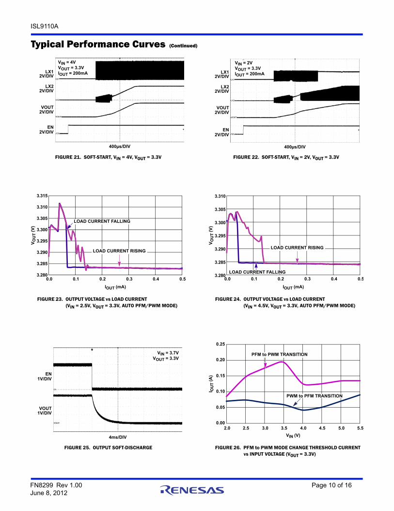
FIGURE 21. SOFT-START, VIN = 4V, VOUT = 3.3V FIGURE 22. SOFT-START, VIN = 2V, VOUT = 3.3V
FIGURE 23. OUTPUT VOLTAGE vs LOAD CURRENT (VIN = 2.5V, VOUT = 3.3V, AUTO PFM/PWM MODE)
FIGURE 24. OUTPUT VOLTAGE vs LOAD CURRENT (VIN = 4.5V, VOUT = 3.3V, AUTO PFM/PWM MODE)
FIGURE 25. OUTPUT SOFT-DISCHARGE FIGURE 26. PFM to PWM MODE CHANGE THRESHOLD CURRENT vs INPUT VOLTAGE (VOUT = 3.3V)
Typical Performance Curves (Continued)
LX12V/DIV
2V/DIVLX2
2V/DIVVOUT
2V/DIVEN
400µs/DIV
VIN = 4VVOUT = 3.3VIOUT = 200mA LX1
2V/DIV
2V/DIVLX2
2V/DIVVOUT
2V/DIVEN
400µs/DIV
VIN = 2VVOUT = 3.3VIOUT = 200mA
3.280
3.285
3.290
3.295
3.300
3.305
3.310
3.315
0.0 0.1 0.2 0.3 0.4 0.5
VO
UT
(V
)
IOUT (mA)
LOAD CURRENT RISING
LOAD CURRENT FALLING
3.280
3.285
3.290
3.295
3.300
3.305
3.310
0.0 0.1 0.2 0.3 0.4 0.5
VO
UT
(V
)
IOUT (mA)
LOAD CURRENT RISING
LOAD CURRENT FALLING
1V/DIVVOUT
1V/DIVEN
4ms/DIV
VIN = 3.7VVOUT = 3.3V
0.00
0.05
0.10
0.15
0.20
0.25
2.0 2.5 3.0 3.5 4.0 4.5 5.0 5.5
I OU
T (
A)
VIN (V)
PFM to PWM TRANSITION
PWM to PFM TRANSITION
FN8299 Rev 1.00 Page 10 of 16June 8, 2012
ISL9110A
Functional DescriptionFunctional OverviewRefer to the “Block Diagram” on page 2. The ISL9110A implements a complete buck boost switching regulator, with PWM controller, internal switches, references, protection circuitry, and control inputs.
The PWM controller automatically switches between buck and boost modes as necessary to maintain a steady output voltage, with changing input voltages and dynamic external loads.
The ISL9110A provides output-power-good and input-power-good open-drain status outputs on pins 7 and 8.
Internal Supply and ReferencesReferring to the “Block Diagram” on page 2, the ISL9110A provides two power input pins. The PVIN pin supplies input power to the DC/DC converter, while the VIN pin provides operating voltage source required for stable VREF generation. Separate ground pins (GND and PGND) are provided to avoid problems caused by ground shift due to the high switching currents.
Enable InputA master enable pin EN allows the device to be enabled. Driving EN low invokes a power-down mode, where most internal device functions, including input and output power good detection, are disabled.
Soft DischargeWhen the device is disabled by driving EN low, an internal resistor between VOUT and GND is activated. This internal resistor has a typical 120Ω resistance.
POR Sequence and Soft-startBringing the EN pin high allows the device to power-up. A number of events occur during the start-up sequence. The internal voltage reference powers up, and stabilizes. The device then starts operating. There is a typical 1ms delay between assertion of the EN pin and the start of switching regulator soft-start ramp.
The soft-start feature minimizes output voltage overshoot and input inrush currents. During soft-start, the reference voltage is ramped to provide a ramping VOUT voltage. While output voltage is lower than approximately 20% of the target output voltage, switching frequency is reduced to a fraction of the normal switching frequency to aid in producing low duty cycles necessary to avoid input inrush current spikes. Once the output voltage exceeds 20% of the target voltage, switching frequency is increased to its nominal value.
When the target output voltage is higher than the input voltage, there will be a transition from buck mode to boost mode during the soft-start sequence. At the time of this transition, the ramp rate of the reference voltage is decreased, such that the output voltage slew rate is decreased. This provides a slower output voltage slew rate.
The VOUT ramp time is not constant for all operating conditions. Soft-start into boost mode will take longer than soft-start into buck mode. The total soft-start time into buck operating mode is
typically 2ms, whereas the typical soft-start time into boost mode operating mode is typically 3ms. Increasing the load current will increase these typical soft-start times.
Overcurrent ProtectionWhen the current in the P-Channel MOSFET is sensed to reach the current limit for 16 consecutive switching cycles, the internal protection circuit is triggered, and switching is stopped for approximately 20ms. The device then performs a soft-start cycle. If the external output overcurrent condition exists after the soft-start cycle, the device will again detect 16 consecutive switching cycles reaching the peak current threshold. The process will repeat as long as the external overcurrent condition is present. This behavior is called ‘hiccup mode’.
Short Circuit ProtectionThe ISL9110A provides short-circuit protection by monitoring the feedback voltage. When feedback voltage is sensed to be lower than a certain threshold, the PWM oscillator frequency is reduced in order to protect the device from damage. The P-Channel MOSFET peak current limit remains active during this state.
Undervoltage LockoutThe undervoltage lockout (UVLO) feature prevents abnormal operation in the event that the supply voltage is too low to guarantee proper operation. When the VIN voltage falls below the UVLO threshold, the regulator is disabled.
PG Status OutputAn open drain output-power-good signal is provided in the ISL9110A. An internal window comparator is used to detect when VOUT is significantly higher or lower than the target output voltage. The PG output will be driven low when sensed VOUT voltage is outside of this ‘power good’ window. When VOUT voltage is inside the ‘power-good’ window, the PG pin goes Hi-Z.
The PG detection circuit detects this condition by monitoring voltage on the FB pin. Hysteresis is provided for the upper and lower PG thresholds to avoid oscillation of the PG output.
BAT Status OutputThe ISL9110A provides an open drain input-power-good status output. The BAT status pin will be driven low when VIN rises above the VTBMON threshold. The BAT status output goes Hi-Z when VBAT falls below the VTBMON threshold. Hysteresis is provided for the VTBMON threshold to avoid oscillation of the BAT output.
Ultrasonic Mode (Available Upon Request)
The ISL9110A provides an ultrasonic mode that can be enabled during IC manufacturing upon request.
In ultrasonic mode, the PFM switching frequency is forced to be above the audio frequency range.
This ultrasonic mode applies only to PFM mode operation. When enabled, the PFM mode switching frequency is forced well above the audio frequency range (fSW becomes typically 60kHz). This mode of operation, however, reduces the efficiency at light load.
FN8299 Rev 1.00 Page 11 of 16June 8, 2012
ISL9110A
Thermal ShutdownA built-in thermal protection feature protects the ISL9110A, if the die temperature reaches +155°C (typical). At this die temperature, the regulator is completely shut down. The die temperature continues to be monitored in this thermal-shutdown mode. When the die temperature falls to +125°C (typical), the device will resume normal operation.
When exiting thermal shutdown, the ISL9110A will execute its soft-start sequence.
External SynchronizationAn external sync feature is provided. Applying a clock signal with a frequency between 2.75MHz and 3.25MHz at the MODE/SYNC input forces the ISL9110A to synchronize to this external clock. The MODE/SYNC input supports standard logic levels.
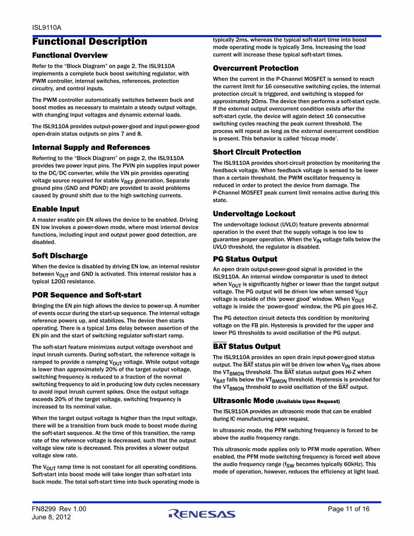
Buck-Boost Conversion TopologyThe ISL9110A operates in either buck or boost mode. When operating in conditions where VIN is close to VOUT, the ISL9110A alternates between buck and boost mode as necessary to provide a regulated output voltage.
Figure 27 shows a simplified diagram of the internal switches and external inductor.
PWM OperationIn buck PWM mode, Switch D is continuously closed, and Switch C is continuously open. Switches A and B operate as a synchronous buck converter when in this mode.
In boost PWM mode, Switch A remains closed and Switch B remains open. Switches C and D operate as a synchronous boost converter when in this mode.
PFM OperationDuring PFM operation in buck mode, Switch D is continuously closed, and Switch C is continuously open. Switches A and B operate in discontinuous mode during PFM operation.
During PFM operation in boost mode, the ISL9110A closes Switch A and Switch C to ramp up the current in the inductor. When inductor current reaches a certain threshold, the device turns off Switches A and C, then turns on Switches B and D. With Switches B and D closed, output voltage increases as the inductor current ramps down.
In most operating conditions, there will be multiple PFM pulses to charge up the output capacitor. These pulses continue until VOUT has achieved the upper threshold of the PFM hysteretic controller. Switching then stops, and remains stopped until VOUT decays to the lower threshold of the hysteretic PFM controller.
Operation With VIN Close to VOUTWhen the output voltage is close to the input voltage, the ISL9110A will rapidly and smoothly switch from boost to buck mode as needed to maintain the regulated output voltage. This behavior provides excellent efficiency and very low output voltage ripple.
Output Voltage ProgrammingThe ISL9110A is available in fixed and adjustable output voltage versions. To use the fixed output version, the VOUT pin must be connected directly to FB.
In the adjustable output voltage version (ISL9110AIITAZ), an external resistor divider is required to program the output voltage. The FB pin has very low input leakage current, so it is possible to use large value resistors (e.g. R1 = 1MΩ and R2 = 324kΩ) in the resistor divider connected to the FB input.
Applications InformationComponent SelectionThe fixed-output version of the ISL9110A requires only three external power components to implement the buck boost converter: an inductor, an input capacitor, and an output capacitor.
The adjustable ISL9110A versions require three additional components to program the output voltage. Two external resistors program the output voltage, and a small capacitor is added to improve stability and response.
An optional input supply filtering capacitor (“C3” in Figure 28) can be used to reduce the supply noise on the VIN pin, which provides power to the internal reference. In most applications, this capacitor is not needed.
FIGURE 27. BUCK BOOST TOPOLOGY
PVIN VOUT
SWITCH A SWITCH D
SWITCH B SWITCH C
LX1 LX2
L1
VOUT =3.0V/1AVOUT
A5
FBD5 C2
10µF
R1
R2
1M
365k
BAT
PGSTATUSOUTPUTS
D2
D1
PVIN
VIN =1.8V TO 5.5V
VIN
B1
C1
MODE
EN
D3
C2
C110µF
ISL9110AIITAZ
D4
C3
LX1
LX2
B2
A4
L12.2µH
C456pF
B5
GND
C5
B3
A3
C4
PGND
B4
A2A1
C31µF
FIGURE 28. TYPICAL ISL9110AIITAZ APPLICATION
FN8299 Rev 1.00 Page 12 of 16June 8, 2012
ISL9110A
Output Voltage Programming, Adj. VersionSetting and controlling the output voltage of the ISL9110AIITAZ (adjustable output version) can be accomplished by selecting the external resistor values.
Equation 1 can be used to derive the R1 and R2 resistor values:
When designing a PCB, include a GND guard band around the feedback resistor network to reduce noise and improve accuracy and stability. Resistors R1 and R2 should be positioned close to the FB pin.
Feed-Forward Capacitor Selection A small capacitor (C4 in Figure 28) in parallel with resistor R1 is required to provide the specified load and line regulation. The suggested value of this capacitor is 56pF for R1 = 1M. An NPO type capacitor is recommended.
Non-Adjustable Version FB Pin ConnectionThe fixed output versions of the ISL9110A does not require external resistors or a capacitor on the FB pin. Simply connect VOUT to FB, as shown in Figure 29.
Inductor SelectionAn inductor with high frequency core material (e.g. ferrite core) should be used to minimize core losses and provide good efficiency. The inductor must be able to handle the peak switching currents without saturating.
A 2.2µH inductor with ≥2.4A saturation current rating is recommended. Select an inductor with low DCR to provide good efficiency. In applications where radiated noise must be minimized, a toroidal or shielded inductor can be used.
PVIN and VOUT Capacitor Selection The input and output capacitors should be ceramic X5R type with low ESL and ESR. The recommended input capacitor value is 10µF. The recommended VOUT capacitor value is 10µF to 22µF.
Application Example 1An application using the fixed-output ISL9110AIITNZ is shown in Figure 30. This application requires only three external components.
Application Example 2An application requiring VOUT = 3.0V, using the adjustable-output ISL9110AIITAZ is shown in Figure 31. This application requires six external components.
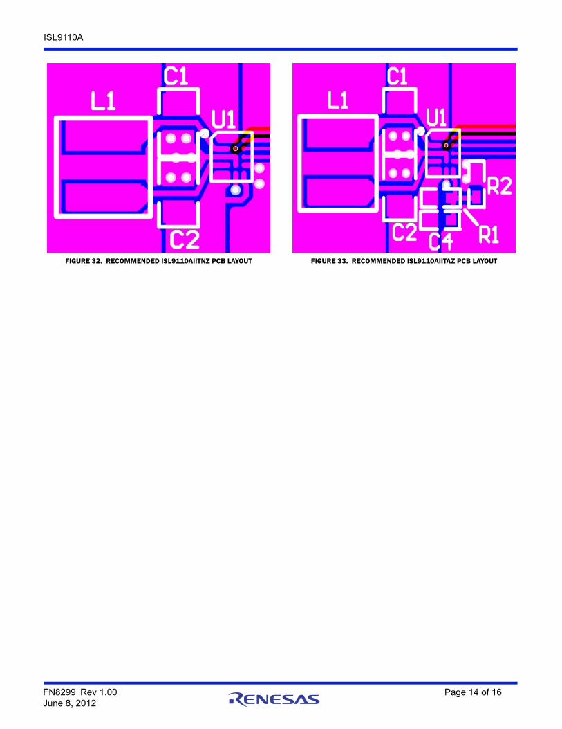
Recommended PCB LayoutCorrect PCB layout is critical for proper operation of the ISL9110A. The input and output capacitors should be positioned as closely to the IC as possible. The ground connections of the input and output capacitors should be kept as short as possible, and should be on the component layer to avoid problems that are caused by high switching currents flowing through PCB vias.
TABLE 1. INDUCTOR VENDOR INFORMATION
MANUFACTURER SERIES WEBSITE
Coilcraft LPS4018 www.coilcraft.com
Murata LQH44P www.murata.com
Taiyo Yuden NRS4018NRS5012
www.t-yuden.com
Sumida CDRH3D23/HPCDRH4D22/HP
www.sumida.com
Toko DEM3518C www.toko.co.jp
VOUT 0.8V 1R1R2--------+
= (EQ. 1)
FIGURE 29. TYPICAL ISL9110AIITNZ APPLICATION
VOUT =3.3V/1AVOUT
A5
FBD5 C2
10µF
BAT
PG
STATUSOUTPUTS
D2
D1
PVIN
VIN =1.8V-5.5V
VIN
B1
C1
MODE
EN
D3
C2
C110µF
ISL9110AIITNZ
D4
C3
LX1
LX2
B2
A4
L12.2µH
B5
GND
C5
B3
A3
C4
PGND
B4
A2A1
TABLE 2. CAPACITOR VENDOR INFORMATION
MANUFACTURER SERIES WEBSITE
AVX X5R www.avx.com
Murata X5R www.murata.com
Taiyo Yuden X5R www.t-yuden.com
TDK X5R www.tdk.com
FIGURE 30. TYPICAL ISL9110AIITNZ APPLICATION
VOUT =3.3V/1AVOUT
A5
FBD5 C2
10µF
BAT
PG
STATUSOUTPUTS
D2
D1
PVIN
VIN =1.8V-5.5V
VIN
B1
C1
MODE
EN
D3
C2
C110µF
ISL9110AIITNZ
D4
C3
LX1
LX2
B2
A4
L12.2µH
B5
GND
C5
B3
A3
C4
PGND
B4
A2A1
FIGURE 31. TYPICAL ISL9110AIITAZ APPLICATION
VOUT =3.0V/1AVOUT
A5
FBD5 C2
10µF
R1
R2
1M
365k
BAT
PG
STATUSOUTPUTS
D2
D1
PVIN
VIN =1.8V-5.5V
VIN
B1
C1
MODE
EN
D3
C2
C110µF
ISL9110AIITAZ
D4
C3
LX1
LX2
B2
A4
L12.2µH
C456pF
B5
GND
C5
B3
A3
C4
PGND
B4
A2A1
FN8299 Rev 1.00 Page 13 of 16June 8, 2012
ISL9110A
FIGURE 32. RECOMMENDED ISL9110AIITNZ PCB LAYOUT FIGURE 33. RECOMMENDED ISL9110AIITAZ PCB LAYOUT
FN8299 Rev 1.00 Page 14 of 16June 8, 2012
ISL9110A
Intersil products are manufactured, assembled and tested utilizing ISO9001 quality systems as notedin the quality certifications found at www.intersil.com/en/support/qualandreliability.html
Intersil products are sold by description only. Intersil may modify the circuit design and/or specifications of products at any time without notice, provided that such modification does not, in Intersil's sole judgment, affect the form, fit or function of the product. Accordingly, the reader is cautioned to verify that datasheets are current before placing orders. Information furnished by Intersil is believed to be accurate and reliable. However, no responsibility is assumed by Intersil or its subsidiaries for its use; nor for any infringements of patents or other rights of third parties which may result from its use. No license is granted by implication or otherwise under any patent or patent rights of Intersil or its subsidiaries.
For information regarding Intersil Corporation and its products, see www.intersil.com
For additional products, see www.intersil.com/en/products.html
© Copyright Intersil Americas LLC 2012. All Rights Reserved.All trademarks and registered trademarks are the property of their respective owners.
ProductsIntersil Corporation is a leader in the design and manufacture of high-performance analog semiconductors. The Company's products address some of the industry's fastest growing markets, such as, flat panel displays, cell phones, handheld products, and notebooks. Intersil's product families address power management and analog signal processing functions. Go to www.intersil.com/products for a complete list of Intersil product families.
For a complete listing of Applications, Related Documentation and Related Parts, please see the respective device information page on intersil.com: ISL9110A
To report errors or suggestions for this datasheet, please go to www.intersil.com/askourstaff
FITs are available from our website at http://rel.intersil.com/reports/search.php
Revision HistoryThe revision history provided is for informational purposes only and is believed to be accurate, but not warranted. Please go to web to make sure you have the latest revision.
DATE REVISION CHANGE
May 29, 2012 FN8299.1 Corrected “Pin Configuration” on page 2.
May 11, 2012 FN8299.0 Initial Release.
FN8299 Rev 1.00 Page 15 of 16June 8, 2012
ISL9110A
FN8299 Rev 1.00 Page 16 of 16June 8, 2012
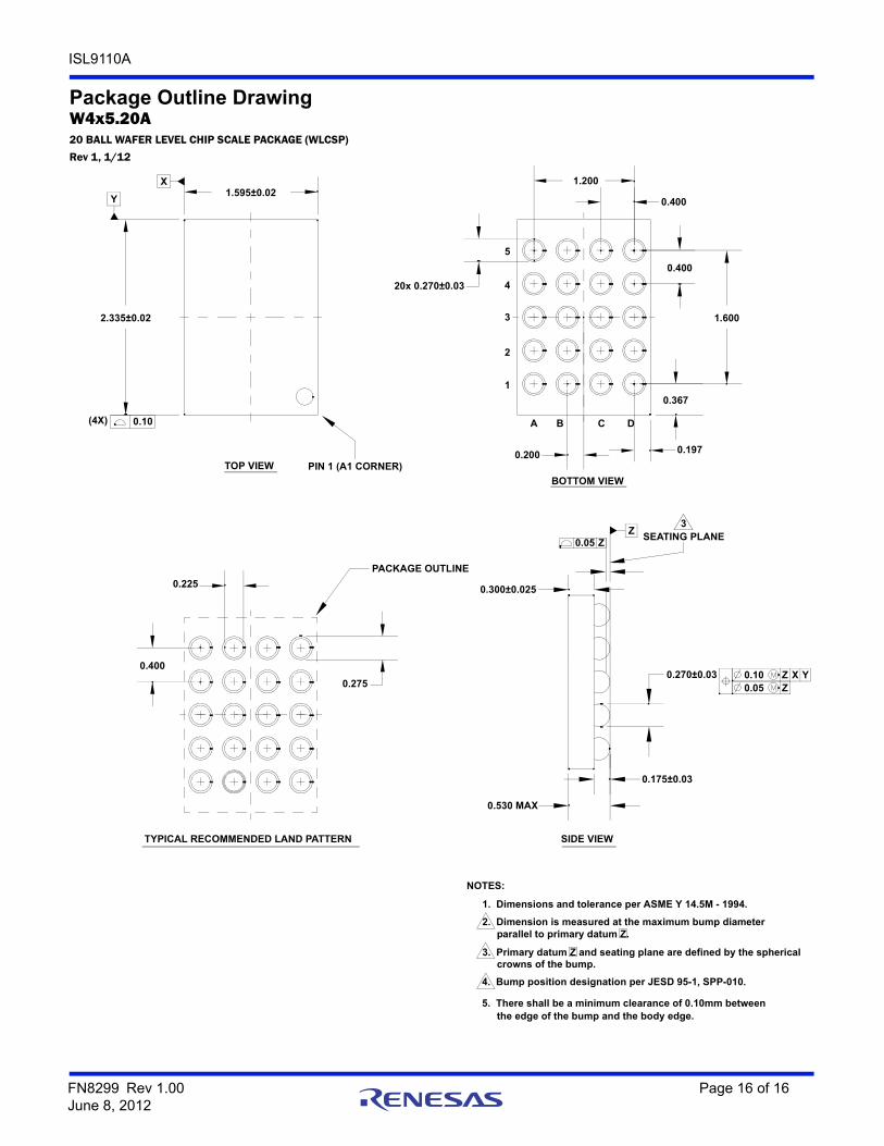
Package Outline DrawingW4x5.20A20 BALL WAFER LEVEL CHIP SCALE PACKAGE (WLCSP)
Rev 1, 1/12
0.270±0.03
0.175±0.03
0.530 MAX
0.300±0.025
SEATING PLANEZ
BOTTOM VIEW
SIDE VIEWTYPICAL RECOMMENDED LAND PATTERN
TOP VIEW PIN 1 (A1 CORNER)
PACKAGE OUTLINE
0.400
0.225
0.10(4X)
0.275
X
Y1.595±0.02
2.335±0.02
1.200
0.400
0.400
1.600
0.367
20x 0.270±0.03
A B C D
0.200
1
2
3
4
5
0.197
0.10 Z X Y0.05 Z
3
0.05 Z
1. Dimensions and tolerance per ASME Y 14.5M - 1994.
2. Dimension is measured at the maximum bump diameter parallel to primary datum Z.
3. Primary datum Z and seating plane are defined by the spherical crowns of the bump.
4. Bump position designation per JESD 95-1, SPP-010.
5. There shall be a minimum clearance of 0.10mm between the edge of the bump and the body edge.
NOTES: