ISL8016 Datasheet - Renesas Electronics
22
FN7616 Rev 1.00 Page 1 of 22 May 5, 2011 FN7616 Rev 1.00 May 5, 2011 ISL8016 6A Low Quiescent Current High Efficiency Synchronous Buck Regulator DATASHEET The ISL8016 is a high efficiency, monolithic, synchronous step-down DC/DC converter that can deliver up to 6A continuous output current from a 2.7V to 5.5V input supply. The output voltage is adjustable from 0.6V to V IN . With an adjustable current limit, reverse current protection, pre-bias start and over temperature protection the ISL8016 offers a highly robust power solution. It uses current control architecture to deliver fast transient response and excellent loop stability. The ISL8016 integrates a pair of low ON-resistance P-Channel and N-Channel internal MOSFETs to maximize efficiency and minimize external component count. 100% duty-cycle operation allows less than 200mV dropout at 6A output current. Adjustable frequency and synchronization allow the ISL8016 to be used in applications requiring low noise. Paralleling capability with phase interleaving allows the IC to support >6A output current while offering reduced input and output noise. The ISL8016 can be configured for discontinuous or forced continuous operation at light load. Forced continuous operation reduces noise and RF interference while discontinuous mode provides high efficiency by reducing switching losses at light loads. The ISL8016 is offered in a space saving 20 Ld 3x4 QFN lead free package with exposed pad lead frames for excellent thermal performance. The complete converter occupies less than 0.15in 2 area. Various fixed output voltages are available upon request. See Ordering Information on page 2 for more detail. Features • High Efficiency Synchronous Buck Regulator with up to 97% Efficiency • 1% Reference Accuracy Over-Temperature/Load/Line • Fixed Output Voltage Option • ±10% Output Voltage Margining • Adjustable Current Limit • Current Sharing Capable • Start-up with Pre-Biased Output • Internal Soft-Start - 1ms or Adjustable, Internal/External Compensation • Soft-Stop Output Discharge During Disabled • Adjustable Frequency from 500kHz to 4MHz - Default at 1MHz • External Synchronization up to 4MHz - Master to Slave Phase Shifting Capability • Peak current limiting, Hiccup Mode Short Circuit Protection and Over-Temperature Protection‘ Applications • DC/DC POL Modules • μC/μP, FPGA and DSP Power • Plug-in DC/DC Modules for Routers and Switchers • Portable Instruments • Test and Measurement Systems • Li-ion Battery Powered Devices FIGURE 1. EFFICIENCY T = +25°C V IN = 5V 70 75 80 85 90 95 100 0.0 1.0 2.0 3.0 4.0 5.0 6.0 I OUT (A) EFFICIENCY (%) 3.3V OUT PFM 3.3V OUT PWM
Transcript of ISL8016 Datasheet - Renesas Electronics

FN7616 Rev 1.00 Page 1 of 22May 5, 2011
FN7616Rev 1.00
May 5, 2011
ISL80166A Low Quiescent Current High Efficiency Synchronous Buck Regulator
DATASHEET
The ISL8016 is a high efficiency, monolithic, synchronous step-down DC/DC converter that can deliver up to 6A continuous output current from a 2.7V to 5.5V input supply. The output voltage is adjustable from 0.6V to VIN. With an adjustable current limit, reverse current protection, pre-bias start and over temperature protection the ISL8016 offers a highly robust power solution. It uses current control architecture to deliver fast transient response and excellent loop stability.
The ISL8016 integrates a pair of low ON-resistance P-Channel and N-Channel internal MOSFETs to maximize efficiency and minimize external component count. 100% duty-cycle operation allows less than 200mV dropout at 6A output current. Adjustable frequency and synchronization allow the ISL8016 to be used in applications requiring low noise. Paralleling capability with phase interleaving allows the IC to support >6A output current while offering reduced input and output noise.
The ISL8016 can be configured for discontinuous or forced continuous operation at light load. Forced continuous operation reduces noise and RF interference while discontinuous mode provides high efficiency by reducing switching losses at light loads.
The ISL8016 is offered in a space saving 20 Ld 3x4 QFN lead free package with exposed pad lead frames for excellent thermal performance. The complete converter occupies less than 0.15in2 area.
Various fixed output voltages are available upon request. See Ordering Information on page 2 for more detail.
Features• High Efficiency Synchronous Buck Regulator with up to 97%
Efficiency
• 1% Reference Accuracy Over-Temperature/Load/Line
• Fixed Output Voltage Option
• ±10% Output Voltage Margining
• Adjustable Current Limit
• Current Sharing Capable
• Start-up with Pre-Biased Output
• Internal Soft-Start - 1ms or Adjustable, Internal/External Compensation
• Soft-Stop Output Discharge During Disabled
• Adjustable Frequency from 500kHz to 4MHz - Default at 1MHz
• External Synchronization up to 4MHz - Master to Slave Phase Shifting Capability
• Peak current limiting, Hiccup Mode Short Circuit Protection and Over-Temperature Protection‘
Applications• DC/DC POL Modules
• µC/µP, FPGA and DSP Power
• Plug-in DC/DC Modules for Routers and Switchers
• Portable Instruments
• Test and Measurement Systems
• Li-ion Battery Powered Devices
FIGURE 1. EFFICIENCY T = +25°C VIN = 5V
70
75
80
85
90
95
100
0.0 1.0 2.0 3.0 4.0 5.0 6.0
IOUT (A)
EF
FIC
IEN
CY
(%
) 3.3VOUT PFM
3.3VOUT PWM

ISL8016
FN7616 Rev 1.00 Page 2 of 22May 5, 2011
Pin ConfigurationISL8016
(20 LD QFN)TOP VIEW
Ordering InformationPART NUMBER(Notes 1, 2, 3) PART MARKING OUTPUT VOLTAGE (V)
TEMP. RANGE (°C)
PACKAGE(Pb-Free)
PKG.DWG. #
ISL8016IRAJZ 016A Adjustable -40 to +85 20 Ld 3x4 QFN L20.3x4
ISL8016IR12Z 016W 1.2V -40 to +85 20 Ld 3x4 QFN L20.3x4
ISL8016IR15Z 016B 1.5V -40 to +85 20 Ld 3x4 QFN L20.3x4
ISL8016IR18Z 016C 1.8V -40 to +85 20 Ld 3x4 QFN L20.3x4
ISL8016IR25Z 016F 2.5V -40 to +85 20 Ld 3x4 QFN L20.3x4
ISL8016IR33Z 016N 3.3V -40 to +85 20 Ld 3x4 QFN L20.3x4
NOTES:
1. Add “-T*” suffix for tape and reel. Please refer to TB347 for details on reel specifications.
2. These Intersil Pb-free plastic packaged products employ special Pb-free material sets, molding compounds/die attach materials, and 100% matte tin plate plus anneal (e3 termination finish, which is RoHS compliant and compatible with both SnPb and Pb-free soldering operations). Intersil Pb-free products are MSL classified at Pb-free peak reflow temperatures that meet or exceed the Pb-free requirements of IPC/JEDEC J STD-020.
3. For Moisture Sensitivity Level (MSL), please see device information page for ISL8016. For more information on MSL please see techbrief TB363.
1
3
4
PGND
PHASE
PHASE
PG
ND
SG
ND
VF
BS
YN
CIN
2
6
97 8
VSET
FS
EN
COMP
VIN
VIN PG
PHASE
5
10
15
13
12
14
11
20 1719 18
16
SY
NC
OU
T
ISET
SS
PG
ND
VIN
PAD
ISL8016
FN7616 Rev 1.00 Page 3 of 22May 5, 2011
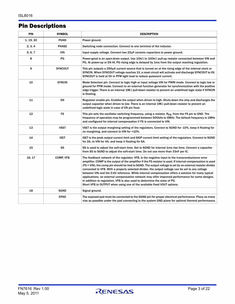
Pin DescriptionsPIN SYMBOL DESCRIPTION
1, 19, 20 PGND Power ground.
2, 3, 4 PHASE Switching node connection. Connect to one terminal of the inductor.
5, 6, 7 VIN Input supply voltage. Connect two 22µF ceramic capacitors to power ground.
8 PG Power-good is an open-drain output. Use 10k to 100k pull-up resistor connected between VIN and PG. At power-up or EN HI, PG rising edge is delayed by 1ms from the output reaching regulation.
9 SYNCOUT This pin outputs a 250µA current source that is turned on at the rising edge of the internal clock or SYNCIN. When SYNCOUT voltage reaches 1V, a reset circuit will activate and discharge SYNCOUT to 0V. SYNCOUT is held at 0V in PFM light load to reduce quiescent current.
10 SYNCIN Mode Selection pin. Connect to logic high or input voltage VIN for PWM mode. Connect to logic low or ground for PFM mode. Connect to an external function generator for synchronization with the positive edge trigger. There is an internal 1M pull-down resistor to prevent an undefined logic state if SYNCIN is floating.
11 EN Regulator enable pin. Enables the output when driven to high. Shuts down the chip and discharges the output capacitor when driven to low. There is an internal 1M pull-down resistor to prevent an undefined logic state in case of EN pin float.
12 FS This pin sets the oscillator switching frequency, using a resistor, RFS, from the FS pin to GND. The frequency of operation may be programmed between 500kHz to 4MHz. The default frequency is 1MHz and configured for internal compensation if FS is connected to VIN.
13 VSET VSET is the output margining setting of the regulators. Connect to SGND for -10%, keep it floating for no margining, and connect to VIN for +10%.
14 ISET ISET is the peak output current limit and SKIP current limit setting of the regulators. Connect to SGND for 2A, to VIN for 4A, and keep it floating for 6A.
15 SS SS is used to adjust the soft-start time. Set to SGND for internal 1ms rise time. Connect a capacitor from SS to SGND to adjust the soft-start time. Do not use more than 33nF per IC.
16, 17 COMP, VFB The feedback network of the regulator, VFB, is the negative input to the transconductance error amplifier. COMP is the output of the amplifier if the FS resistor is used. If internal compensation is used (FS = VIN), the comp pin should be tied to SGND. The output voltage is set by an external resistor divider connected to VFB. With a properly selected divider, the output voltage can be set to any voltage between VIN and the 0.6V reference. While internal compensation offers a solution for many typical applications, an external compensation network may offer improved performance for some designs. In addition to regulation, VFB is also used to determine the state of PG.Short VFB to OUTPUT when using one of the available fixed VOUT options.
18 SGND Signal ground.
EPAD The exposed pad must be connected to the SGND pin for proper electrical performance. Place as many vias as possible under the pad connecting to the system GND plane for optimal thermal performance.

ISL8016
FN7616 Rev 1.00 Page 4 of 22May 5, 2011
Typical Application Diagrams
L1.0µH
PHASE
PGND
VFB
VIN
EN
PG
SYNCOUT
INPUT 2.7V TO 5.5VOUTPUT
1.8V/6A
C1ISL8016
C2
R2200k
R3100k
2x47µF
SS
SGND
C3*10pF
R1100k
FIGURE 2. TYPICAL APPLICATION DIAGRAM - SINGLE CHIP 6A
COMP
SYNCIN
FS
ISET
VSET
VIN
* C3 is optional. Recommend putting a placeholder for it. Checkloop analysis first before use.
2x22µF
TABLE 1. COMPONENT VALUE SELECTION
VOUT 0.8V 1.2V 1.5V 1.8V 2.5V 3.3V 3.6V
C1 44µF 44µF 44µF 44µF 44µF 44µF 44µF
C2 (or C8) 2x47µF 2x47µF 2x47µF 2x47µF 2x47µF 2x47µF 2x47µF
C3 (or C5) 10pF 10pF 10pF 10pF 10pF 10pF 10pF
L1 (or L2) 0.47~1µH 0.47~1µH 0.47~1µH 0.68~1.5µH 0.68~1.5µH 1~2.2µH 1~2.2µH
R2 (or R5) 33k 100k 150k 200k 316k 450k 500k
R3 (or R6) 100k 100k 100k 100k 100k 100k 100k
ISL8016
FN7616 Rev 1.00 Page 5 of 22May 5, 2011
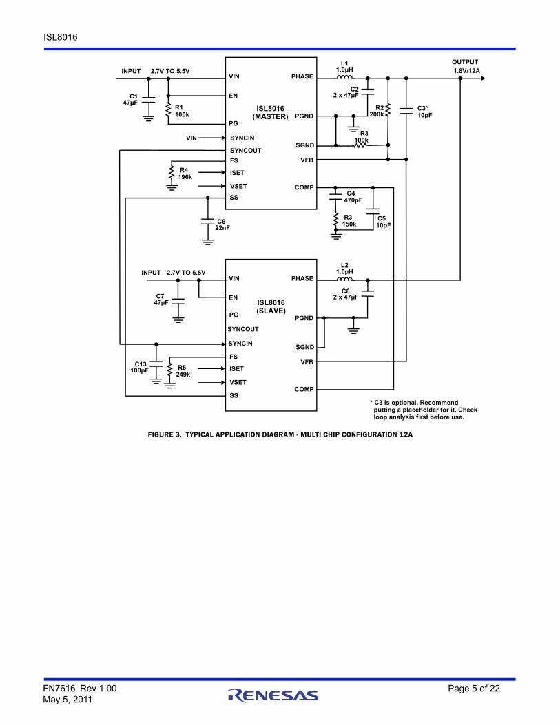
FIGURE 3. TYPICAL APPLICATION DIAGRAM - MULTI CHIP CONFIGURATION 12A
L21.0µH
PHASE
PGND
VFB
VIN
EN
PG
INPUT 2.7V TO 5.5V
C747µF ISL8016
C82 x 47µF
SS
SGND
C4470pF
COMP
L11.0µH
PHASE
PGND
VFB
VIN
EN
PG
INPUT 2.7V TO 5.5V
OUTPUT1.8V/12A
C147µF
ISL8016
C2
R2200k
R3100k
2 x 47µF
SS
SGND
C3*10pF
R1100k
COMP
VIN
R3150k
C510pF
C622nF
SYNCOUT
SYNCIN
FS
ISET
VSET
FS
ISET
VSET
SYNCIN
SYNCOUT
* C3 is optional. Recommend putting a placeholder for it. Checkloop analysis first before use.
C13100pF
(MASTER)
(SLAVE)
R4196k
R5249k

ISL8016
FN7616 Rev 1.00 Page 6 of 22May 5, 2011
Block Diagram
FIGURE 4. FUNCTIONAL BLOCK DIAGRAM
PHASE
++
CSA
+
+
OCP
SKIP
+
+
+
SlopeCOMPSLOPE
SoftSTARTSOFT
EAMPCOMP
PWM/PFMLOGIC
CONTROLLERPROTECTION
HS DRIVER
VFB
+0.85*VREF
PG
SYNCIN
SHUTDOWN
VIN
PGND
OSCILLATOR
ZERO-CROSSSENSING
BANDGAP
SCP
+0.1V
EN
SHUTDOWN
1msDELAY
55pF
168k
SGND
3pF
6k
-
- -
-
-
--
VDD
SS
COMP
100
SHUTDOWN
LSDRIVER
SYNCOUTFS
ISETTHRESHOLD
ISET
VSET
VREF
+
NEG CURRENTSENSING
250µA
P
N
+
0.8V-
UV
OV

ISL8016
FN7616 Rev 1.00 Page 7 of 22May 5, 2011
Absolute Maximum Ratings (Reference to GND) Thermal InformationVIN . . . . . . . . . . . . . . . . . . . . . . . . . . . . . . . . -0.3V to 5.8V (DC) or 7V (20ms)EN, FS, ISET, PG, SYNCOUT, SYNCIN VFB, VSET . . . . . . . -0.3V to VIN+0.3VPHASE . . . . . . . . . . . . -1.5V (100ns)/-0.3V (DC) to 6.5V (DC) or 7V (20ms)COMP, SS . . . . . . . . . . . . . . . . . . . . . . . . . . . . . . . . . . . . . . . . . . . -0.3V to 2.7VESD Rating
Human Body Model (Tested per JESD22-A114) . . . . . . . . . . . . . . . . . 3kVMachine Model (Tested per JESD22-A115). . . . . . . . . . . . . . . . . . . . 300VCharged Device Model (Tested per JESD22-C101E). . . . . . . . . . . . 1500V
Latch Up (Tested per JESD-78A; Class 2, Level A) . . . . . .100mA @ +85°C
Thermal Resistance (Typical) JA (°C/W) JC (°C/W)3x4 QFN Package (Notes 4, 5) . . . . . . . . . . 42 5
Junction Temperature Range . . . . . . . . . . . . . . . . . . . . . . .-55°C to +125°CStorage Temperature Range. . . . . . . . . . . . . . . . . . . . . . . .-65°C to +150°CPb-Free Reflow Profile . . . . . . . . . . . . . . . . . . . . . . . . . . . . . . . see link below
http://www.intersil.com/pbfree/Pb-FreeReflow.asp
Recommended Operating ConditionsVIN Supply Voltage Range . . . . . . . . . . . . . . . . . . . . . . . . . . . . . . 2.7V to 5.5VLoad Current Range . . . . . . . . . . . . . . . . . . . . . . . . . . . . . . . . . . . . . . 0A to 6AAmbient Temperature Range . . . . . . . . . . . . . . . . . . . . . . . . -40°C to +85°C
CAUTION: Do not operate at or near the maximum ratings listed for extended periods of time. Exposure to such conditions may adversely impact productreliability and result in failures not covered by warranty.
NOTES:
4. JA is measured in free air with the component mounted on a high effective thermal conductivity test board with “direct attach” features. See Tech Brief TB379.
5. JC, “case temperature” location is at the center of the exposed metal pad on the package underside.
Analog Specifications Unless otherwise noted, all parameter limits are established over the recommended operating conditions and the typical specification are measured at the following conditions: TA = -40°C to +85°C, VIN = 3.6V, EN = VIN, unless otherwise noted. Typical values are at TA = +25°C. Boldface limits apply over the operating temperature range, -40°C to +85°C.
PARAMETER SYMBOL TEST CONDITIONSMIN
(Note 6) TYPMAX
(Note 6) UNITS
INPUT SUPPLY
VIN Undervoltage Lockout Threshold VUVLO Rising, no load 2.5 2.7 V
Falling, no load 2.2 2.4 V
Quiescent Supply Current IVIN SYNCIN = GND, no load at the output 70 µA
SYNCIN = GND, no load at the output and no switches switching
70 90 µA
SYNCIN = VIN, FS = 1MHz, no load at the output 8 15 mA
Shut Down Supply Current ISD SYNCIN = GND, VIN = 5.5V, EN = low 5 7 µA
OUTPUT REGULATION
Reference Voltage - ISL8016IRAJZ VREF VSET = VIN 0.651 0.660 0.669 V
VSET = FLOAT 0.594 0.600 0.606 V
VSET = SGND 0.531 0.540 0.549 V
Output Voltage - ISL8016IR12Z VVFB VSET = FLOAT 1.188 1.200 1.212 V
Output Voltage - ISL8016IR15Z VVFB VSET = FLOAT 1.485 1.500 1.515 V
Output Voltage - ISL8016IR18Z VVFB VSET = FLOAT 1.782 1.800 1.818 V
Output Voltage - ISL8016IR25Z VVFB VSET = FLOAT 2.475 2.500 2.525 V
Output Voltage - ISL8016IR33Z VVFB VSET = FLOAT 3.266 3.300 3.333 V
Output Voltage Margining VVFB VSET = VIN, Percent of OUTPUT changed 9.5 10 10.5 %
VSET = SGND, Percent of OUTPUT changed -10.5 -10 -9.5 %
VFB Bias Current - ISL8016IRAJZ IVFB VFB = 0.75V 0.1 µA
Fixed Output VFB Bias Current - ISL8016IRXXZ IVFB VSET = FLOAT, VFB = 10% above OUTPUT 6 µA
Line Regulation VIN = VO + 0.5V to 5.5V (minimal 2.7V) 0.2 %/V
Soft-Start Ramp Time Cycle SS = SGND 1 ms
Soft-Start Charging Current ISS VSS = 0.1V 1.4 1.8 2.2 µA

ISL8016
FN7616 Rev 1.00 Page 8 of 22May 5, 2011
OVERCURRENT PROTECTION
Current Limit Blanking Time tOCON 17 Clock pulses
Overcurrent and Auto Restart Period tOCOFF 8 SS cycle
Positive Peak Current Limit IPLIMIT ISET = FLOAT 7.7 9.5 11.5 A
ISET = VIN 5.5 6.5 8.0 A
ISET = SGND 3 4.0 5 A
Peak Skip Limit ISKIP ISET = FLOAT 1.6 2 2.4 A
ISET = VIN 1.0 1.35 1.6 A
ISET = SGND 0.85 A
Zero Cross Threshold -300 300 mA
Negative Current Limit INLIMIT -4.25 -3 -1.75 A
COMPENSATION
Error Amplifier Trans-Conductance FS = VIN 100 µA/V
FS with Resistor 200 µA/V
Trans-Resistance RT 0.117 0.138 0.16
PHASE
P-Channel MOSFET ON-Resistance VIN = 5V, IO = 200mA 31 45 m
VIN = 2.7V, IO = 200mA 44 55 m
N-Channel MOSFET ON-Resistance VIN = 5V, IO = 200mA 19 35 m
VIN = 2.7V, IO = 200mA 25 50 m
PHASE Maximum Duty Cycle 100
PHASE Minimum On-Time SYNCIN = High 140 ns
OSCILLATOR
Nominal Switching Frequency Fsw FS = VIN 800 1000 1200 kHz
FS with RS = 402k 450 525 600 kHz
FS with RS = 42.4k 3300 3900 4500 kHz
SYNCIN Logic Low to High Transition Range 0.70 0.75 0.80 V
SYNCIN Hysteresis 0.15 V
SYNCIN Logic Input Leakage Current VIN = 3.6V 3.6 5 µA
SYNCOUT Charging Current ISO PWM 210 250 290 µA
PFM 0 µA
SYNCOUT Voltage Low 0.3 V
PG
Output Low Voltage 0.3 V
Delay Time (Rising Edge) 0.5 1 2 ms
PG Pin Leakage Current 0.01 0.1 µA
OVP PG Rising Threshold 0.80 V
UVP PG Rising Threshold 80 85 90 %
Analog Specifications Unless otherwise noted, all parameter limits are established over the recommended operating conditions and the typical specification are measured at the following conditions: TA = -40°C to +85°C, VIN = 3.6V, EN = VIN, unless otherwise noted. Typical values are at TA = +25°C. Boldface limits apply over the operating temperature range, -40°C to +85°C. (Continued)
PARAMETER SYMBOL TEST CONDITIONSMIN
(Note 6) TYPMAX
(Note 6) UNITS

ISL8016
FN7616 Rev 1.00 Page 9 of 22May 5, 2011
UVP PG Hysteresis 5 %
PGOOD Delay Time (Falling Edge) 7 µs
ISET, VSET
Logic Input Low 0.4 V
Logic Input Float 0.5 0.8 V
Logic Input High 0.9 V
Logic Input Leakage Current 0.1 1 µA
EN
Logic Input Low 0.4 V
Logic Input High 0.9 V
EN Logic Input Leakage Current 0.1 1 µA
Thermal Shutdown 150 °C
Thermal Shutdown Hysteresis 25 °C
NOTE:6. Compliance to datasheet limits is assured by one or more methods: production test, characterization and/or design.
Analog Specifications Unless otherwise noted, all parameter limits are established over the recommended operating conditions and the typical specification are measured at the following conditions: TA = -40°C to +85°C, VIN = 3.6V, EN = VIN, unless otherwise noted. Typical values are at TA = +25°C. Boldface limits apply over the operating temperature range, -40°C to +85°C. (Continued)
PARAMETER SYMBOL TEST CONDITIONSMIN
(Note 6) TYPMAX
(Note 6) UNITS

ISL8016
FN7616 Rev 1.00 Page 10 of 22May 5, 2011
Typical Operating Performance Unless otherwise noted, operating conditions are: TA = +25°C, VIN = 5V, EN = 3.3V, SYNCIN = VIN, L = 1.0µH, C1 = 2x22µF, C2 = 4x22µF, VOUT = 1.8V, IOUT = 0A to 6A.
FIGURE 5. EFFICIENCY vs LOAD (1MHz 3.3VIN PWM) FIGURE 6. EFFICIENCY vs LOAD (1MHz 3.3VIN PFM)
FIGURE 7. EFFICIENCY vs LOAD (1MHz 5VIN PWM) FIGURE 8. EFFICIENCY vs LOAD (1MHz 5VIN PFM)
FIGURE 9. POWER DISSIPATION vs LOAD (1MHz, VOUT = 1.8V) FIGURE 10. VOUT REGULATION vs VIN (PWM VOUT = 1.8V)
70
75
80
85
90
95
100
0.0 1.0 2.0 3.0 4.0 5.0 6.0
EF
FIC
IEN
CY
(%
)
IOUT (A)
1.2VOUT
1.8VOUT
2.5VOUT
1.5VOUT
70
75
80
85
90
95
100
0.0 0.3 0.6 0.9 1.2 1.5 1.8
EF
FIC
IEN
CY
(%
)
IOUT (A)
1.2VOUT 1.8VOUT
2.5VOUT
1.5VOUT
EF
FIC
IEN
CY
(%
)
IOUT (A)
70
75
80
85
90
95
100
0.0 1.0 2.0 3.0 4.0 5.0 6.0
1.2VOUT
1.8VOUT
2.5VOUT
1.5VOUT
3.3VOUT
EF
FIC
IEN
CY
(%
)
IOUT (A)
70
75
80
85
90
95
100
0.0 0.3 0.6 0.9 1.2 1.5 1.8
3.3VOUT
1.2VOUT 1.8VOUT2.5VOUT 1.5VOUT
PD
(W
)
IOUT (A)
0
0.3
0.6
0.9
1.2
1.5
1.8
0.0 1.0 2.0 3.0 4.0 5.0 6.0
5VIN PWM MODE
3.3VIN PWM MODE
VO
UT (
V)
VIN (V)
1.78
1.79
1.80
1.81
1.82
1.83
1.84
2.5 3.0 3.5 4.0 4.5 5.0 5.5
3A LOAD
6A LOAD
0A LOAD

ISL8016
FN7616 Rev 1.00 Page 11 of 22May 5, 2011
FIGURE 11. VOUT REGULATION vs VIN (PFM VOUT = 1.8V) FIGURE 12. VOUT REGULATION vs LOAD (1MHz, VOUT = 1.2V)
FIGURE 13. VOUT REGULATION vs LOAD (1MHz, VOUT = 1.5V) FIGURE 14. VOUT REGULATION vs LOAD (1MHz, VOUT = 1.8V)
FIGURE 15. VOUT REGULATION vs LOAD (1MHz, VOUT = 2.5V) FIGURE 16. VOUT REGULATION vs LOAD (1MHz, VOUT = 3.3V)
Typical Operating Performance Unless otherwise noted, operating conditions are: TA = +25°C, VIN = 5V, EN = 3.3V, SYNCIN = VIN, L = 1.0µH, C1 = 2x22µF, C2 = 4x22µF, VOUT = 1.8V, IOUT = 0A to 6A. (Continued)
VO
UT (
V)
VIN (V)
1.78
1.79
1.80
1.81
1.82
1.83
1.84
2.5 3.0 3.5 4.0 4.5 5.0 5.5
3A LOAD
6A LOAD
0A LOAD
VO
UT (
V)
IOUT (A)
1.18
1.19
1.20
1.21
1.22
1.23
1.24
0.0 1.0 2.0 3.0 4.0 5.0 6.0
3.3VIN PWM MODE
5VIN PFM MODE5VIN PWM MODE
3.3VIN PFM MODE
VO
UT (
V)
IOUT (A)
1.48
1.49
1.50
1.51
1.52
1.53
1.54
0.0 1.0 2.0 3.0 4.0 5.0 6.0
3.3VIN PWM MODE
5VIN PFM MODE
5VIN PWM MODE 3.3VIN PFM MODE
VO
UT (
V)
IOUT (A)
1.78
1.79
1.80
1.81
1.82
1.83
1.84
0.0 1.0 2.0 3.0 4.0 5.0 6.0
3.3VIN PWM MODE
5VIN PFM MODE
5VIN PWM MODE3.3VIN PFM MODE
VO
UT (
V)
IOUT (A)
2.48
2.49
2.50
2.51
2.52
2.53
2.54
0.0 1.0 2.0 3.0 4.0 5.0 6.0
3.3VIN PWM MODE
5VIN PFM MODE
5VIN PWM MODE3.3VIN PFM MODE
VO
UT (
V)
IOUT (A)
3.31
3.32
3.33
3.34
3.35
3.36
3.37
0.0 1.0 2.0 3.0 4.0 5.0 6.0
5VIN PFM MODE
5VIN PWM MODE

ISL8016
FN7616 Rev 1.00 Page 12 of 22May 5, 2011
FIGURE 17. STEADY STATE OPERATION AT NO LOAD (PWM) FIGURE 18. STEADY STATE OPERATION AT NO LOAD (PFM)
FIGURE 19. STEADY STATE OPERATION WITH FULL LOAD FIGURE 20. LOAD TRANSIENT (PWM)
FIGURE 21. LOAD TRANSIENT (PFM) FIGURE 22. SOFT-START WITH NO LOAD (PWM)
Typical Operating Performance Unless otherwise noted, operating conditions are: TA = +25°C, VIN = 5V, EN = 3.3V, SYNCIN = VIN, L = 1.0µH, C1 = 2x22µF, C2 = 4x22µF, VOUT = 1.8V, IOUT = 0A to 6A. (Continued)
PHASE 2V/DIV
VOUT RIPPLE 20mV/DIV
IL 1A/DIV
PHASE 2V/DIV
VOUT RIPPLE 20mV/DIV
IL 1A/DIV
PHASE 2V/DIV
VOUT RIPPLE 20mV/DIV
IL 2A/DIV
VOUT RIPPLE 50mV/DIV
IL 2A/DIV
VOUT RIPPLE 50mV/DIV
IL 52A/DIV
EN 2V/DIV
VOUT 1V/DIV
IL 1A/DIV
PG 5V/DIV

ISL8016
FN7616 Rev 1.00 Page 13 of 22May 5, 2011
FIGURE 23. SOFT-START AT NO LOAD (PFM) FIGURE 24. SOFT-START WITH PRE-BIASED 1V
FIGURE 25. SOFT-START AT FULL LOAD FIGURE 26. SOFT-DISCHARGE SHUTDOWN
FIGURE 27. STEADY STATE OPERATION AT NO LOAD WITH FREQUENCY = 2MHz
FIGURE 28. STEADY STATE OPERATION AT FULL LOAD WITH FREQUENCY = 2MHz
Typical Operating Performance Unless otherwise noted, operating conditions are: TA = +25°C, VIN = 5V, EN = 3.3V, SYNCIN = VIN, L = 1.0µH, C1 = 2x22µF, C2 = 4x22µF, VOUT = 1.8V, IOUT = 0A to 6A. (Continued)
EN 2V/DIV
VOUT 1V/DIV
IL 1A/DIV
PG 5V/DIV
EN 2V/DIV
VOUT 1V/DIV
IL 1A/DIV
PG 5V/DIV
EN 2V/DIV
VOUT 1V/DIV
IL 2A/DIV
PG 5V/DIV
EN 2V/DIV
VOUT 1V/DIV
IL 1A/DIV
PG 5V/DIV
PHASE 5V/DIV
IL 0.5A/DIV
SYNC 5V/DIV
VOUT RIPPLE 20mV/DIV
PHASE 5V/DIV
IL 2A/DIV
SYNC 5V/DIV
VOUT RIPPLE 20mV/DIV

ISL8016
FN7616 Rev 1.00 Page 14 of 22May 5, 2011
FIGURE 29. STEADY STATE OPERATION AT NO LOAD WITH FREQUENCY = 4MHz
FIGURE 30. STEADY STATE OPERATION AT FULL LOAD (PWM) WITH FREQUENCY = 4MHz
FIGURE 31. OUTPUT SHORT CIRCUIT FIGURE 32. OUTPUT SHORT CIRCUIT RECOVERY
Typical Operating Performance Unless otherwise noted, operating conditions are: TA = +25°C, VIN = 5V, EN = 3.3V, SYNCIN = VIN, L = 1.0µH, C1 = 2x22µF, C2 = 4x22µF, VOUT = 1.8V, IOUT = 0A to 6A. (Continued)
PHASE 5V/DIV
IL 0.2A/DIV
SYNC 5V/DIV
VOUT RIPPLE 20mV/DIV
PHASE 5V/DIV
IL 2A/DIV
SYNC 5V/DIV
VOUT RIPPLE 20mV/DIV
PHASE 5V/DIV
VOUT 1V/DIV
IL 2A/DIV
PG 5V/DIV
PHASE 5V/DIV
VOUT 1V/DIV
IL 5A/DIV
PG 5V/DIV

ISL8016
FN7616 Rev 1.00 Page 15 of 22May 5, 2011
Theory of OperationThe ISL8016 is a step-down switching regulator optimized for battery-powered handheld applications. The regulator operates at 1MHz fixed default switching frequency when FS is connected to VIN. By connecting a resistor from FS to SGND, the operating frequency may be adjusted from 500kHz to 4MHz. Unless forced, PWM is chosen (SYNCIN pulled HI), the regulator will allow PFM operation and reduce switching frequency at light loading to maximize efficiency. In this condition, no load quiescent is typically 70µA.
PWM Control SchemePulling the SYNCIN high (>0.8V) forces the converter into PWM mode, regardless of output current. The ISL8016 employs the current-mode pulse-width modulation (PWM) control scheme for fast transient response and pulse-by-pulse current limiting. Figure 4 shows the block diagram. The current loop consists of the oscillator, the PWM comparator, current sensing circuit and the slope compensation for the current loop stability. The slope compensation is 360mV/Ts. Current sense resistance, Rt, is typically 0.138V/A. The control reference for the current loop comes from the error amplifier's (EAMP) output.
The PWM operation is initialized by the clock from the oscillator. The P-Channel MOSFET is turned on at the beginning of a PWM cycle and the current in the MOSFET starts to ramp up. When the sum of the current amplifier CSA and the slope compensation reaches the control reference of the current loop, the PWM comparator EAMP output sends a signal to the PWM logic to turn off the P-FET and turn on the N-Channel MOSFET. The N-FET stays on until the end of the PWM cycle. Figure 33 shows the typical operating waveforms during the PWM operation. The dotted lines illustrate the sum of the slope compensation ramp and the current-sense amplifier’s CSA output.
The output voltage is regulated by controlling the VEAMP voltage to the current loop. The bandgap circuit outputs a 0.6V reference voltage to the voltage loop. The feedback signal comes from the VFB pin. The soft-start block only affects the operation during the start-up and will be discussed separately. The error amplifier is a transconductance amplifier that converts the voltage error signal to a current output. The voltage loop is internally compensated with the 55pF and 168kΩ RC network. The maximum EAMP voltage output is precisely clamped to 2.4V.
SKIP ModePulling the SYNCIN pin LO (<0.4V) forces the converter into PFM mode. The ISL8016 enters a pulse-skipping mode at light load to minimize the switching loss by reducing the switching frequency. Figure 34 illustrates the skip-mode operation. A zero-cross sensing circuit shown in Figure 4 monitors the N-FET current for zero crossing. When 8 consecutive cycles of the inductor current crossing zero are detected, the regulator enters the skip mode. During the eight detecting cycles, the current in the inductor is allowed to become negative. The counter is reset to zero when the current in any cycle does not cross zero.
Once the skip mode is entered, the pulse modulation starts being controlled by the SKIP comparator shown in Figure 34. Each pulse cycle is still synchronized by the PWM clock. The P-FET is turned on at the clock's rising edge and turned off when the output is higher than 1.5% of the nominal regulation or when its current reaches the peak Skip current limit value. Then the inductor current is discharging to 0A and stays at zero. The internal clock is disabled. The output voltage reduces gradually due to the load current discharging the output capacitor. When the output voltage drops to the nominal voltage, the P-FET will be turned on again at the rising edge of the internal clock as it repeats the previous operations.
The regulator resumes normal PWM mode operation when the output voltage drops 1.5% below the nominal voltage.
FIGURE 33. PWM OPERATION WAVEFORMS
VEAMP
VCSA
DUTYCYCLE
IL
VOUT
FIGURE 34. SKIP MODE OPERATION WAVEFORMS
CLOCK
IL
VOUT
NOMINAL
PFM CURRENT LIMIT
0
8 CYCLES
SYNCOUT
PWM PFM
NOMINAL -1.5%
PWM
LOAD CURRENT
0.8V
NOMINAL +1.5%
ISL8016
FN7616 Rev 1.00 Page 16 of 22May 5, 2011
Frequency AdjustThe frequency of operation is fixed at 1MHz and internal compensation when FS is tied to VIN. Adjustable frequency ranges from 500kHz to 4MHz via a simple resistor connecting FS to SGND according to Equation 1:
Figure 35 is a graph of the measured Frequency vs RT for a VIN of 2.7V and 5.5V.
Synchronization ControlThe ISL8016 can be synchronized from 500kHz to 4MHz by an external signal applied to the SYNCIN pin. SYNCIN frequency should be greater than 50% of internal clock frequency. The rising edge on the SYNCIN triggers the rising edge of the PHASE pulse. Make sure that the minimum on time of the PHASE node is greater than 140ns.
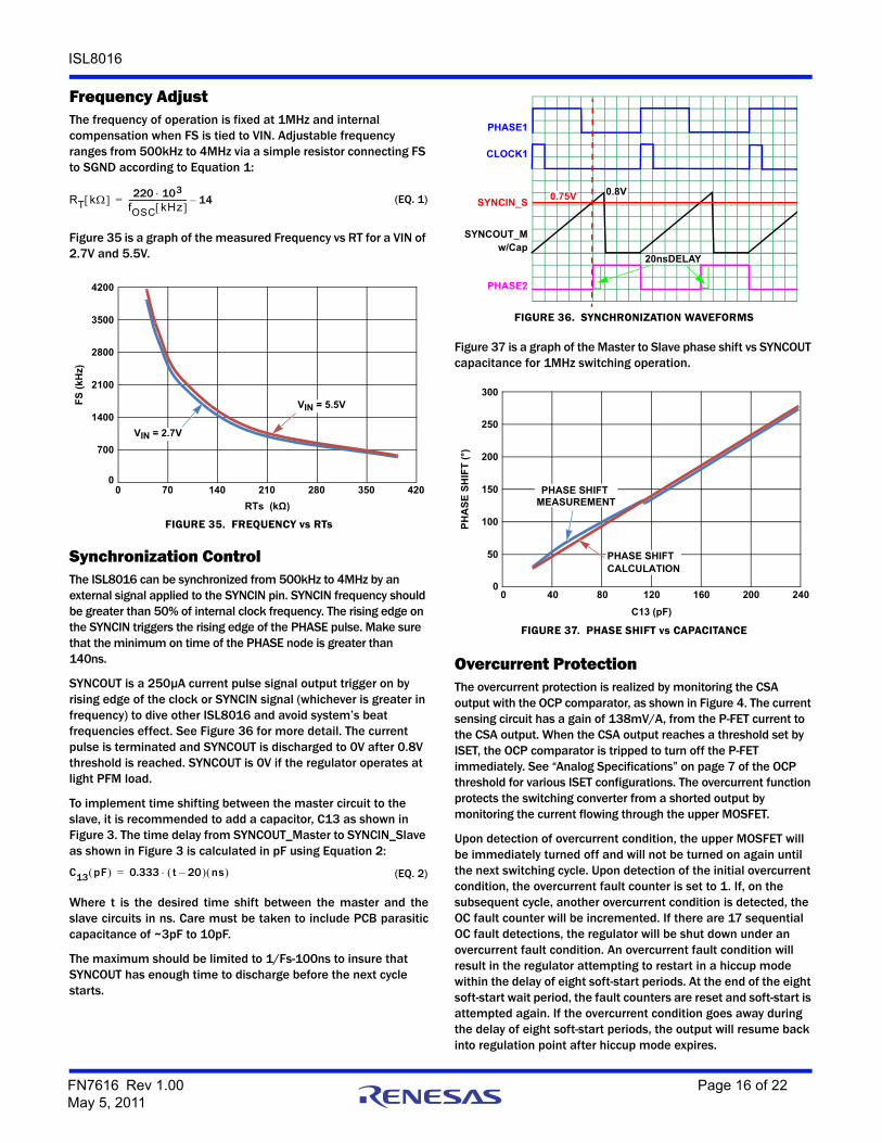
SYNCOUT is a 250µA current pulse signal output trigger on by rising edge of the clock or SYNCIN signal (whichever is greater in frequency) to dive other ISL8016 and avoid system’s beat frequencies effect. See Figure 36 for more detail. The current pulse is terminated and SYNCOUT is discharged to 0V after 0.8V threshold is reached. SYNCOUT is 0V if the regulator operates at light PFM load.
To implement time shifting between the master circuit to the slave, it is recommended to add a capacitor, C13 as shown in Figure 3. The time delay from SYNCOUT_Master to SYNCIN_Slave as shown in Figure 3 is calculated in pF using Equation 2:
Where t is the desired time shift between the master and theslave circuits in ns. Care must be taken to include PCB parasiticcapacitance of ~3pF to 10pF.
The maximum should be limited to 1/Fs-100ns to insure that SYNCOUT has enough time to discharge before the next cycle starts.
Figure 37 is a graph of the Master to Slave phase shift vs SYNCOUT capacitance for 1MHz switching operation.
Overcurrent ProtectionThe overcurrent protection is realized by monitoring the CSA output with the OCP comparator, as shown in Figure 4. The current sensing circuit has a gain of 138mV/A, from the P-FET current to the CSA output. When the CSA output reaches a threshold set by ISET, the OCP comparator is tripped to turn off the P-FET immediately. See “Analog Specifications” on page 7 of the OCP threshold for various ISET configurations. The overcurrent function protects the switching converter from a shorted output by monitoring the current flowing through the upper MOSFET.
Upon detection of overcurrent condition, the upper MOSFET will be immediately turned off and will not be turned on again until the next switching cycle. Upon detection of the initial overcurrent condition, the overcurrent fault counter is set to 1. If, on the subsequent cycle, another overcurrent condition is detected, the OC fault counter will be incremented. If there are 17 sequential OC fault detections, the regulator will be shut down under an overcurrent fault condition. An overcurrent fault condition will result in the regulator attempting to restart in a hiccup mode within the delay of eight soft-start periods. At the end of the eight soft-start wait period, the fault counters are reset and soft-start is attempted again. If the overcurrent condition goes away during the delay of eight soft-start periods, the output will resume back into regulation point after hiccup mode expires.
RT k 220 103fOSC kHz ------------------------------ 14–= (EQ. 1)
FIGURE 35. FREQUENCY vs RTs
0
700
1400
2100
2800
3500
4200
0 70 140 210 280 350 420
RTs (kΩ)
FS
(kH
z)
VIN = 2.7V
VIN = 5.5V
C13 pF 0.333 t 20– ns = (EQ. 2)
FIGURE 36. SYNCHRONIZATION WAVEFORMS
PHASE1
CLOCK1
SYNCOUT_Mw/Cap
SYNCIN_S
PHASE2
0.8V0.75V
20nsDELAY
0
50
100
150
200
250
300
0 40 80 120 160 200 240
C13 (pF)
PH
AS
E S
HIF
T (
°)
FIGURE 37. PHASE SHIFT vs CAPACITANCE
PHASE SHIFT MEASUREMENT
PHASE SHIFT CALCULATION

ISL8016
FN7616 Rev 1.00 Page 17 of 22May 5, 2011
Negative Current ProtectionSimilar to the overcurrent, the negative current protection is realized by monitoring the current across the low-side N-FET, as shown in Figure 4. When the valley point of the inductor current reaches -3A for 4 consecutive cycles, both P-FET and N-FET are off. The 100Ω in parallel to the N-FET will activate discharging the output into regulation. The control will begin to switch when output is within regulation. The regulator will be in PFM for 20µs before switching to PWM if necessary.
PG PG is an open-drain output of a window comparator that continuously monitors the buck regulator output voltage. PG is actively held low when EN is low and during the buck regulator soft-start period. After 1ms delay of the soft-start period, PG becomes high impedance as long as the output voltage is within nominal regulation voltage set by VFB. When VFB drops 15% below or raises 0.8V above the nominal regulation voltage, the ISL8016 pulls PG low. Any fault condition forces PG low until the fault condition is cleared by attempts to soft-start. For logic level output voltages, connect an external pull-up resistor, R1, between PG and VIN. A 100kΩ resistor works well in most applications.
UVLOWhen the input voltage is below the undervoltage lock-out (UVLO) threshold, the regulator is disabled.
Soft Start-UpThe soft start-up reduces the in-rush current during the start-up. The soft-start block outputs a ramp reference to the input of the error amplifier. This voltage ramp limits the inductor current as well as the output voltage speed so that the output voltage rises in a controlled fashion. When VFB is less than 0.1V at the beginning of the soft-start, the switching frequency is reduced to 200kHz so that the output can start-up smoothly at light load condition. During soft-start, the IC operates in the SKIP mode to support pre-biased output condition.
Tie SS to SGND for an internal soft-start of approximately 1ms. Connect a capacitor from SS to SGND to adjust the soft-start time. This capacitor, along with an internal 1.6µA current source sets the soft-start interval of the converter, tSS.
CSS must be less than 33nF to insure proper soft-start reset after fault condition.
Figure 38 is a comparison between measured and calculated output soft-start time versus Css capacitance.
EnableThe enable (EN) input allows the user to control the turning on or off of the regulator for purposes such as power-up sequencing. When the regulator is enabled, there is typically a 600µs delay for waking up the bandgap reference and then the soft start-up begins.
Discharge Mode (Soft-Stop)When a transition to shutdown mode occurs or the VIN UVLO is set, the outputs discharge to GND through an internal 100Ω switch. The discharge mode is disabled if SS is tied to an external capacitor.
Power MOSFETsThe power MOSFETs are optimized for best efficiency. The ON-resistance for the P-FET is typically 30mΩ and the ON-resistance for the N-FET is typically 20mΩ.
100% Duty CycleThe ISL8016 features 100% duty cycle operation to maximize the battery life. When the battery voltage drops to a level that the ISL8016 can no longer maintain the regulation at the output, the regulator completely turns on the P-FET. The maximum dropout voltage under the 100% duty-cycle operation is the product of the load current and the ON-resistance of the P-FET.
Thermal ShutdownThe ISL8016 has built-in thermal protection. When the internal temperature reaches +150°C, the regulator is completely shut down. As the temperature drops to +125°C, the ISL8016 resumes operation by stepping through the soft-start.
CSS F 3.33 tSS s = (EQ. 3)
0
3
6
9
12
15
18
0 8 16 24 32 40 48
CSS (nF)
VS
S (
ms
)
FIGURE 38. SOFT-START TIME vs CSS
SS (ms) MEASUREMENT
SS (ms)CALCULATION

ISL8016
FN7616 Rev 1.00 Page 18 of 22May 5, 2011
Applications Information Output Inductor and Capacitor SelectionTo consider steady state and transient operations, ISL8016 typically uses a 1.0µH output inductor. The higher or lower inductor value can be used to optimize the total converter system performance. For example, for higher output voltage 3.3V application, in order to decrease the inductor current ripple and output voltage ripple, the output inductor value can be increased. It is recommended to set the ripple inductor current approximately 30% of the maximum output current for optimized performance. The inductor ripple current can be expressed as shown in Equation 4:
The inductor’s saturation current rating needs to be at least larger than the peak current. The ISL8016 protects the typical peak current of 9A. The saturation current needs be over 12A for maximum output current application.
The ISL8016 uses an internal compensation network and the output capacitor value is dependent on the output voltage. The ceramic capacitor is recommended to be X5R or X7R.
In Table 1, the minimum output capacitor value is given for the different output voltages to make sure that the whole converter system is stable. Additional output capacitance may be added for improved transient response.
Output Voltage SelectionThe output voltage of the regulator can be programmed via an external resistor divider that is used to scale the output voltage relative to the internal reference voltage and feed it back to the inverting input of the error amplifier (refer to Figure 2).
The output voltage programming resistor, R2, will depend on the value chosen for the feedback resistor and the desired output voltage of the regulator. The value for the feedback resistor is typically between 10kΩ and 100kΩas shown in Equation 5.
If the output voltage desired is 0.6V, then R3 is left unpopulated and R2 is shorted. There is a leakage current from VIN to PHASE. It is recommended to preload the output with 10µA minimum. Capacitance, C3, maybe added to improve transient performance. A good starting point for C3 can be determined by choosing a value that provides an 80kHz corner frequency with R2.
VSET marginally adjusts VFB according to the “Analog Specifications” on page 7.
Figure 39 is the recommended minimum output voltage setting vs operational frequency in order to avoid the minimum On-Time specification.
Input Capacitor SelectionThe main functions for the input capacitor are to provide decoupling of the parasitic inductance and to provide filtering function to prevent the switching current flowing back to the battery rail. At least two 22µF X5R or X7R ceramic capacitors are a good starting point for the input capacitor selection.
Loop Compensation DesignWhen there is an external resistor connected from FS to SGND, the COMP pin is active for external loop compensation. The ISL8016 uses constant frequency peak current mode control architecture to achieve fast loop transient response. An accurate current sensing pilot device in parallel with the upper MOSFET is used for peak current control signal and overcurrent protection. The inductor is not considered as a state variable since its peak current is constant, and the system becomes single order system. It is much easier to design a type II compensator to stabilize the loop than to implement voltage mode control. Peak current mode control has inherent input voltage feed-forward function to achieve good line regulation. Figure 40 shows the small signal model of the synchronous buck regulator.
I
VO 1VOVIN--------–
L fS------------------------------------=
(EQ. 4)
R2 R3
VOVFB---------- 1– = (EQ. 5)
FIGURE 39. MINIMUM VOUT vs FREQUENCY
0.0
0.5
1.0
1.5
2.0
2.5
3.0
0.5 1.0 1.5 2.0 2.5 3.0 3.5 4.0FREQUENCY (MHz)
VO
UT (
V)
VIN = 3.3V
VIN = 5V
+
1:D
+
Co
Rc
-Av(S)
d
RT
He(S)+
K
ov
VINd
LP
+
1:D
+
Rc
Ro
RT
Fm
Ti(S)
K
o
TV(S)
VIN^
^
^
^
^
FIGURE 40. SMALL SIGNAL MODEL OF SYNCHRONOUS BUCK REGULATOR
RLP
ILd
IIN^ IL
^
VCOMP

ISL8016
FN7616 Rev 1.00 Page 19 of 22May 5, 2011
PWM COMPARATOR GAIN Fm:The PWM comparator gain Fm for peak current mode control is given by Equation 6:
Where, Se is the slew rate of the slope compensation and Sn is given by Equation 7:
Where Rt is trans-resistance, which is the gain of the current amplifier.
CURRENT SAMPLING TRANSFER FUNCTION He(S):In current loop, the current signal is sampled every switching cycle. It has the following transfer function:
where Qn and n are given by
Power Stage Transfer FunctionsTransfer function F1(S) from control to output voltage is:
Where
Transfer function F2(S) from control to inductor current is given by Equation 10:
where .
Current loop gain Ti(S) is expressed as Equation 11:
The voltage loop gain with open current loop is:
The Voltage loop gain with current loop closed is given by Equation 13:
Where is the feedback voltage of the voltage error amplifier. If Ti(S)>>1, then Equation 13 can be simplified by Equation 14:
From Equation 14, it is shown that the system is a single order system, which has a single pole located at before the half switching frequency. Therefore, a simple type II compensator can be easily used to stabilize the system.
Figure 41 shows the type II compensator and its transfer function is expressed as follows:
Where
Compensator design goal:
High DC gain
Loop bandwidth fc:
Gain margin: >10dB
Phase margin: 40°
The compensator design procedure is as follows:
Put compensator zero
Put one compensator pole at zero frequency to achieve high DC gain, and put another compensator pole at either ESR zero frequency or half switching frequency, whichever is lower. An optional zero can boost the phase margin. CZ2 is a zero due to R2 and C3
Put compensator zero
The loop gain Tv(S) at cross over frequency of fc has unity gain. Therefore, the compensator resistance R6 is determined by:
Fmd
vcomp---------------- 1
Se Sn+ Ts------------------------------= = (EQ. 6)
Sn Rt
Vin Vo–
LP--------------------= (EQ. 7)
He S S2
n2
-------=S
nQn-------------- 1+ + (EQ. 8)
Qn2---–= n fs=
F1 S vod
------ Vin
1 Sesr------------+
S2
o2
------- SoQp-------------- 1+ +
--------------------------------------= = (EQ. 9)
esr1
RcCo------------- Qp Ro
CoLP------ o
1
LPCo
-----------------=,,=
F2 S Iod----
VinRo RLP+-----------------------
1Sz------+
S2
o2
------- SoQp-------------- 1+ +
--------------------------------------= = (EQ. 10)
z1
RoCo-------------=
Ti S RtFmF2 S He S = (EQ. 11)
Tv S KFmF1 S Av S = (EQ. 12)
Lv S Tv S
1 Ti S +-----------------------= (EQ. 13)
KVFBVo
--------- VFB,=
Lv S VFBVo
---------Ro RLP+
Rt-----------------------
1S
esr------------+
1Sp-------+
----------------------Av S
He S --------------- p
1RoCo-------------,= (EQ. 14)
p
-
+
R6
VREF
VFB
Vo
GM
VCOMP
C7
-
+
C6
FIGURE 41. TYPE II COMPENSATOR
C3R2
R3
Av S vcomp
vFB---------------- GM
C6 C7+-------------------
1S
cz1------------+
1S
cz2------------+
S 1S
cp----------+
---------------------------------------------------------==
(EQ. 15)
cz11
R6C6-------------- cz2
1R2C3--------------= cp
C6 C7+
R6C6C7---------------------=,=
14---to
110-------
fs
cz1 1to3 1RoCo-------------=
cz2 5to8 1RoCo-------------=
R6
2fcVoCoRtGM VFB
--------------------------------= (EQ. 16)

ISL8016
FN7616 Rev 1.00 Page 20 of 22May 5, 2011
where GM is the sum of the trans-conductance, gm, of the voltage error amplifier in each phase. Compensator capacitor C6 is then given by:
Example: VIN = 5V, Vo = 2.5V, Io = 6A, fs = 1MHz, Co = 44µF/3mΩ, L = 1µH, GM = 100µs, Rt = 0.25V/A, VFB = 0.6V, Se = 0.15V/µs, Sn = 2.55105V/s, fc = 100kHz, then compensator resistance R6 = 120kΩ.
Put the compensator zero at 1.5kHz (~1.5x CoRo), and put the compensator pole at ESR zero which is 390kHz. The compensator capacitors are:
C6 = 220pF, C7 = 3pF (there is approximately 3pF parasitic capacitance from VCOMP to GND; therefore, C7 optional).
Figure 42 shows the simulated loop gain response. It is shown that it has 95kHz loop bandwidth with 79° phase margin and at least 10dB gain margin.
PCB Layout RecommendationThe PCB layout is a very important converter design step to make sure the designed converter works well. For ISL8016, the power loop is composed of the output inductor L’s, the output capacitor COUT, the PHASE’s pins, and the PGND pin. It is necessary to make the power loop as small as possible and the connecting traces among them should be direct, short and wide. The switching node of the converter, the PHASE pins, and the traces connected to the node are very noisy, so keep the voltage feedback trace away from these noisy traces. The input capacitor should be placed as close as possible to the VIN pin , and the ground of the input and output capacitors should be connected as close as possible. The heat of the IC is mainly dissipated through the thermal pad. Maximizing the copper area connected to the thermal pad is preferable. In addition, a solid ground plane is helpful for better EMI performance. It is recommended to add at least 5 vias ground connection within the pad for the best thermal relief.
C61
R6cz----------------- C7
12R6fesr-------------------------=,= (EQ. 17)
100 1k 10k 100k 1M-30
-15
0
15
30
45
60
GAIN LOOP (dB)
0
30
60
90
120
150
PHASE LOOP (°)
100 1k 10k 100k 1M
FIGURE 42. SIMULATED LOOP GAIN
180

FN7616 Rev 1.00 Page 21 of 22May 5, 2011
ISL8016
Intersil products are manufactured, assembled and tested utilizing ISO9001 quality systems as notedin the quality certifications found at www.intersil.com/en/support/qualandreliability.html
Intersil products are sold by description only. Intersil may modify the circuit design and/or specifications of products at any time without notice, provided that such modification does not, in Intersil's sole judgment, affect the form, fit or function of the product. Accordingly, the reader is cautioned to verify that datasheets are current before placing orders. Information furnished by Intersil is believed to be accurate and reliable. However, no responsibility is assumed by Intersil or its subsidiaries for its use; nor for any infringements of patents or other rights of third parties which may result from its use. No license is granted by implication or otherwise under any patent or patent rights of Intersil or its subsidiaries.
For information regarding Intersil Corporation and its products, see www.intersil.com
For additional products, see www.intersil.com/en/products.html
© Copyright Intersil Americas LLC 2011. All Rights Reserved.All trademarks and registered trademarks are the property of their respective owners.
ProductsIntersil Corporation is a leader in the design and manufacture of high-performance analog semiconductors. The Company's products address some of the industry's fastest growing markets, such as, flat panel displays, cell phones, handheld products, and notebooks. Intersil's product families address power management and analog signal processing functions. Go to www.intersil.com/products for a complete list of Intersil product families.
*For a complete listing of Applications, Related Documentation and Related Parts, please see the respective device information page on intersil.com: ISL8016
To report errors or suggestions for this datasheet, please go to: www.intersil.com/askourstaff
FITs are available from our website at: http://rel.intersil.com/reports/sear
Revision HistoryThe revision history provided is for informational purposes only and is believed to be accurate, but not warranted. Please go to web to make sure you have the latest Rev.
DATE REVISION CHANGE
4/21/11 FN7616.1 Figures 6 and 8 - smoothed curves.
3/31/11 FN7616.0 Initial Release.

ISL8016
FN7616 Rev 1.00 Page 22 of 22May 5, 2011
Package Outline Drawing
L20.3x420 LEAD QUAD FLAT NO-LEAD PLASTIC PACKAGERev 1, 3/10
TYPICAL RECOMMENDED LAND PATTERN
DETAIL "X"
TOP VIEW
BOTTOM VIEW
SIDE VIEW
located within the zone indicated. The pin #1 indentifier may be
Unless otherwise specified, tolerance : Decimal ± 0.05
Tiebar shown (if present) is a non-functional feature.
The configuration of the pin #1 identifier is optional, but must be
between 0.15mm and 0.30mm from the terminal tip.Dimension applies to the metallized terminal and is measured
Dimensions in ( ) for Reference Only.
Dimensioning and tolerancing conform to AMSE Y14.5m-1994.
6.
either a mold or mark feature.
3.
5.
4.
2.
Dimensions are in millimeters.1.
NOTES:
0.10 M C A B
M C0.05
0.15
0.08 C
0.10 C
A
B
C
C
4.00
3.00
20x 0.40±0.10
2.65
1.65
0.25
0.50
(2.80)
(1.65)
+0.10-0.15
+0.10-0.15
+0.05-0.0720X
A
A
4
(4X)
SEATING PLANE
0.9± 0.10
50.2 REF
0.05 MAX.
SEE DETAIL "X"
0.00 MIN.
(C 0.40)
1
2017
16
116
10 7
(3.80)
(2.65)
(20 x 0.25)
(20 x 0.60)
(16 x 0.50)
16X
VIEW "A-A"
PIN 1 INDEX AREA
PIN 1INDEX AREA
6
6