12-Bit High Speed Micro Power Sampling Analog-To-Digital Converter
24
ADS7816 DESCRIPTION The ADS7816 is a 12-bit, 200kHz sampling analog- to-digital converter. It features low power operation with automatic power down, a synchronous serial interface, and a differential input. The reference volt- age can be varied from 100mV to 5V, with a corre- sponding resolution from 24μV to 1.22mV. Low power, automatic power down, and small size make the ADS7816 ideal for battery operated systems or for systems where a large number of signals must be acquired simultaneously. It is also ideal for remote and/or isolated data acquisition. The ADS7816 is available in an 8-pin plastic mini-DIP, an 8-lead SOIC, or an 8-lead MSOP package. 12-Bit High Speed Micro Power Sampling ANALOG-TO-DIGITAL CONVERTER ® © 1996 Burr-Brown Corporation PDS-1355B Printed in U.S.A., March, 1997 International Airport Industrial Park • Mailing Address: PO Box 11400, Tucson, AZ 85734 • Street Address: 6730 S. Tucson Blvd., Tucson, AZ 85706 • Tel: (520) 746-1111 • Twx: 910-952-1111 Internet: http://www.burr-brown.com/ • FAXLine: (800) 548-6133 (US/Canada Only) • Cable: BBRCORP • Telex: 066-6491 • FAX: (520) 889-1510 • Immediate Product Info: (800) 548-6132 FEATURES ● 200kHz SAMPLING RATE ● MICRO POWER: 1.9mW at 200kHz 150μ W at 12.5kHz ● POWER DOWN: 3μA Max ● 8-PIN MINI-DIP, SOIC, AND MSOP ● DIFFERENTIAL INPUT ● SERIAL INTERFACE APPLICATIONS ● BATTERY OPERATED SYSTEMS ● REMOTE DATA ACQUISITION ● ISOLATED DATA ACQUISITION SAR Control Serial Interface D OUT Comparator S/H Amp CS/SHDN DCLOCK +In V REF –In CDAC OPA658 ADS7816 ADS7816 SBAS061
Transcript of 12-Bit High Speed Micro Power Sampling Analog-To-Digital Converter

ADS7816
DESCRIPTIONThe ADS7816 is a 12-bit, 200kHz sampling analog-to-digital converter. It features low power operationwith automatic power down, a synchronous serialinterface, and a differential input. The reference volt-age can be varied from 100mV to 5V, with a corre-sponding resolution from 24µV to 1.22mV.
Low power, automatic power down, and small sizemake the ADS7816 ideal for battery operated systemsor for systems where a large number of signals must beacquired simultaneously. It is also ideal for remoteand/or isolated data acquisition. The ADS7816 isavailable in an 8-pin plastic mini-DIP, an 8-lead SOIC,or an 8-lead MSOP package.
12-Bit High Speed Micro Power SamplingANALOG-TO-DIGITAL CONVERTER
®
©1996 Burr-Brown Corporation PDS-1355B Printed in U.S.A., March, 1997
International Airport Industrial Park • Mailing Address: PO Box 11400, Tucson, AZ 85734 • Street Address: 6730 S. Tucson Blvd., Tucson, AZ 85706 • Tel: (520) 746-1111 • Twx: 910-952-1111Internet: http://www.burr-brown.com/ • FAXLine: (800) 548-6133 (US/Canada Only) • Cable: BBRCORP • Telex: 066-6491 • FAX: (520) 889-1510 • Immediate Product Info: (800) 548-6132
FEATURES 200kHz SAMPLING RATE
MICRO POWER:1.9mW at 200kHz150µW at 12.5kHz
POWER DOWN: 3µA Max
8-PIN MINI-DIP, SOIC, AND MSOP
DIFFERENTIAL INPUT
SERIAL INTERFACE
APPLICATIONS BATTERY OPERATED SYSTEMS
REMOTE DATA ACQUISITION
ISOLATED DATA ACQUISITION
SAR Control
Serial Interface
DOUT
ComparatorS/H AmpCS/SHDN
DCLOCK
+In
VREF
–InCDAC
OPA658
ADS7816ADS7816
SBAS061
2
®
ADS7816
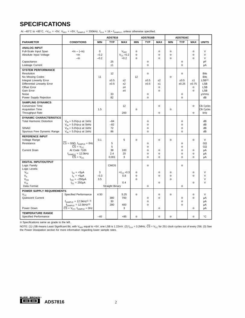
SPECIFICATIONS At –40°C to +85°C, +VCC = +5V, VREF = +5V, fSAMPLE = 200kHz, fCLK = 16 • fSAMPLE, unless otherwise specified.
ADS7816 ADS7816B ADS7816C
PARAMETER CONDITIONS MIN TYP MAX MIN TYP MAX MIN TYP MAX UNITS
ANALOG INPUTFull-Scale Input Span +In – (–In) 0 VREF VAbsolute Input Voltage +In –0.2 VCC +0.2 V
–In –0.2 +0.2 VCapacitance 25 pFLeakage Current ±1 µA
SYSTEM PERFORMANCEResolution 12 BitsNo Missing Codes 11 12 BitsIntegral Linearity Error ±0.5 ±2 ±0.5 ±2 ±0.5 ±1 LSB(1)
Differential Linearity Error ±0.5 ±2 ±0.5 ±1 ±0.25 ±0.75 LSBOffset Error ±4 LSBGain Error ±4 LSBNoise 33 µVrmsPower Supply Rejection 82 dB
SAMPLING DYNAMICSConversion Time 12 Clk CyclesAcquisition Time 1.5 Clk CyclesThroughput Rate 200 kHz
DYNAMIC CHARACTERISTICSTotal Harmonic Distortion VIN = 5.0Vp-p at 1kHz –84 dB
VIN = 5.0Vp-p at 5kHz –82 dBSINAD VIN = 5.0Vp-p at 1kHz 72 dBSpurious Free Dynamic Range VIN = 5.0Vp-p at 1kHz 86 dB
REFERENCE INPUTVoltage Range 0.1 5 VResistance CS = GND, fSAMPLE = 0Hz 5 GΩ
CS = VCC 5 GΩCurrent Drain At Code 710h 38 100 µA
fSAMPLE = 12.5kHz 2.4 20 µACS = VCC 0.001 3 µA
DIGITAL INPUT/OUTPUTLogic Family CMOS
Logic Levels:VIH IIH = +5µA 3 +VCC +0.3 V
VIL IIL = +5µA –0.3 0.8 V VOH IOH = –250µA 3.5 V VOL IOL = 250µA 0.4 V Data Format Straight Binary
POWER SUPPLY REQUIREMENTSVCC Specified Performance 4.50 5.25 VQuiescent Current 380 700 µA
fSAMPLE = 12.5kHz(2, 3) 30 µAfSAMPLE = 12.5kHz(3) 280 400 µA
Power Down CS = VCC, fSAMPLE = 0Hz 3 µA
TEMPERATURE RANGESpecified Performance –40 +85 °C
Specifications same as grade to the left.
NOTE: (1) LSB means Least Significant Bit, with VREF equal to +5V, one LSB is 1.22mV. (2) fCLK = 3.2MHz, CS = VCC for 251 clock cycles out of every 256. (3) Seethe Power Dissipation section for more information regarding lower sample rates.

3
®
ADS7816
The information provided herein is believed to be reliable; however, BURR-BROWN assumes no responsibility for inaccuracies or omissions. BURR-BROWNassumes no responsibility for the use of this information, and all use of such information shall be entirely at the user’s own risk. Prices and specifications are subjectto change without notice. No patent rights or licenses to any of the circuits described herein are implied or granted to any third party. BURR-BROWN does notauthorize or warrant any BURR-BROWN product for use in life support devices and/or systems.
ELECTROSTATICDISCHARGE SENSITIVITY
Electrostatic discharge can cause damage ranging from per-formance degradation to complete device failure. Burr-Brown Corporation recommends that all integrated circuitsbe handled and stored using appropriate ESD protectionmethods.
ESD damage can range from subtle performance degrada-tion to complete device failure. Precision integrated circuitsmay be more susceptible to damage because very smallparametric changes could cause the device not to meetpublished specifications.
ABSOLUTE MAXIMUM RATINGS (1)
+VCC ..................................................................................................... +6VAnalog Input ........................................................... –0.3V to (+VCC + 0.3V)Logic Input ............................................................. –0.3V to (+VCC + 0.3V)Case Temperature ......................................................................... +100°CJunction Temperature .................................................................... +150°CStorage Temperature ..................................................................... +125°CExternal Reference Voltage .............................................................. +5.5V
NOTE: (1) Stresses above these ratings may permanently damage the device.
PIN CONFIGURATION
PIN ASSIGNMENTSPIN NAME DESCRIPTION
1 VREF Reference Input.
2 +In Non Inverting Input.
3 –In Inverting Input. Connect to ground or to remote ground sense point.
4 GND Ground.
5 CS/SHDN Chip Select when LOW, Shutdown Mode when HIGH.
6 DOUT The serial output data word is comprised of 12 bits of data. In operation the data is valid on the falling edge of DCLOCK. Thesecond clock pulse after the falling edge of CS enables the serial output. After one null bit the data is valid for the next 12 edges.
7 DCLOCK Data Clock synchronizes the serial data transfer and determines conversion speed.
8 +VCC Power Supply.
PACKAGE/ORDERING INFORMATION
MAXIMUM MAXIMUMINTEGRAL DIFFERENTIAL PACKAGE
LINEARITY ERROR LINEARITY ERROR TEMPERATURE DRAWINGPRODUCT (LSB) (LSB) RANGE PACKAGE NUMBER (1)
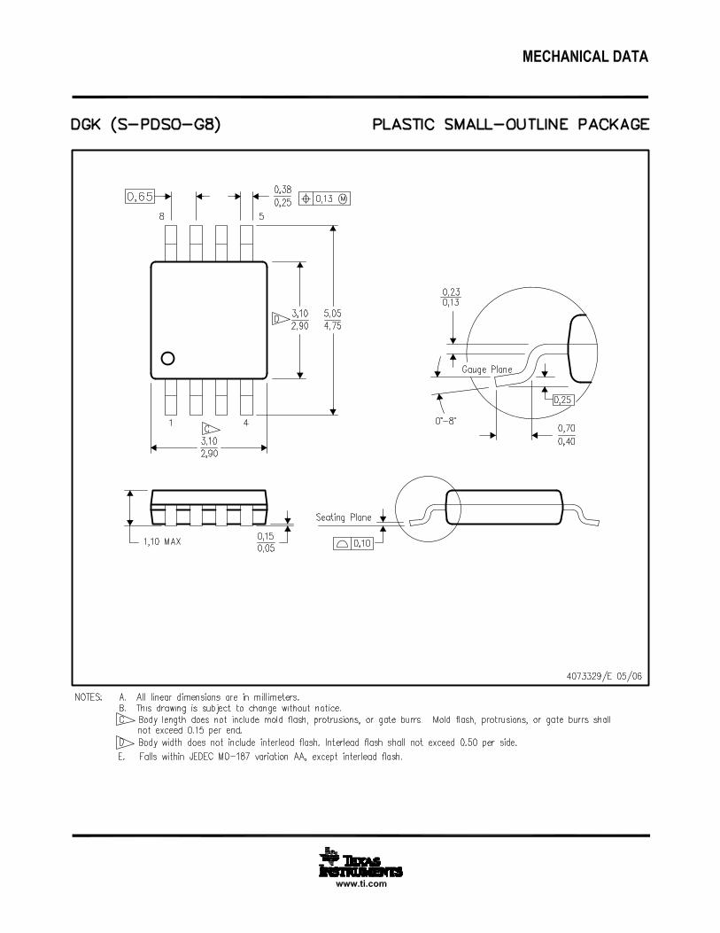
ADS7816P ±2 ±2 –40°C to +85°C Plastic DIP 006ADS7816U ±2 ±2 –40°C to +85°C SOIC 182ADS7816E ±2 ±2 –40°C to +85°C MSOP 337ADS7816PB ±2 ±1 –40°C to +85°C Plastic DIP 006ADS7816UB ±2 ±1 –40°C to +85°C SOIC 182ADS7816EB ±2 ±1 –40°C to +85°C MSOP 337ADS7816PC ±1 ±0.75 –40°C to +85°C Plastic DIP 006ADS7816UC ±1 ±0.75 –40°C to +85°C SOIC 182ADS7816EC ±1 ±0.75 –40°C to +85°C MSOP 337
NOTE: (1) For detailed drawing and dimension table, please see end of data sheet, or Appendix C of Burr-Brown IC Data Book.
1
2
3
4
8
7
6
5
+VCC
DCLOCK
DOUT
CS/SHDN
VREF
+In
–In
GND
ADS7816
8-Pin PDIP, 8-Lead SOIC, 8-Lead MSOP

4
®
ADS7816
TYPICAL PERFORMANCE CURVESAt TA = +25°C, VCC = +5V, VREF = +5V, fSAMPLE = 200kHz, and fCLK = 16 • fSAMPLE, unless otherwise specified.
CHANGE IN OFFSET vs REFERENCE VOLTAGE5
4.5
4
3.5
3
2.5
2
1.5
1
0.5
0
Cha
nge
in O
ffset
(LS
B)
1 2 3 4 5Reference Voltage (V)
CHANGE IN OFFSET vs TEMPERATURE0.6
0.4
0.2
0
–0.2
–0.4
–0.6
Del
ta fr
om 2
5°C
(LS
B)
–55 –40 –25 0 25 70 85
Temperature (°C)
CHANGE IN GAIN vs REFERENCE VOLTAGE4
3.5
3
2.5
2
1.5
1
0.5
0
Cha
nge
in G
ain
(LS
B)
1 2 3 4 5Reference Voltage (V)
CHANGE IN GAIN vs TEMPERATURE0.15
0.1
0.05
0
–0.05
–0.1
–0.15
Del
ta fr
om 2
5°C
(LS
B)
–55 –40 –25 0 25 70 85
Temperature (°C)
EFFECTIVE NUMBER OF BITS vs REFERENCE VOLTAGE
12
11.75
11.5
11.25
11
10.75
10.5
10.25
10
Effe
ctiv
e N
umbe
r of
Bits
(rm
s)
0.1 1 10
Reference Voltage (V)
PEAK-TO-PEAK NOISE vs REFERENCE VOLTAGE10
9
8
7
6
5
4
3
2
1
0
Pea
k-to
-Pea
k N
oise
(LS
B)
0.1 1 10
Reference Voltage (V)

5
®
ADS7816
SIGNAL-TO-(NOISE + DISTORTION) vs INPUT LEVEL80
70
60
50
40
30
20
10
0Sig
nal-t
o-(N
oise
Rat
io P
lus
Dis
tort
ion)
(dB
)
–40 –35 –30 –25 –20 –15 –10 –5 0
Input Level (dB)
SIGNAL-TO-(NOISE + DISTORTION) vs FREQUENCY100
90
80
70
60
50
40
30
20
10
0
Sig
nal-t
o-(N
oise
+ D
isto
rtio
n) (
dB)
1 10 100
Frequency (kHz)
TYPICAL PERFORMANCE CURVES (CONT)At TA = +25°C, VCC = +5V, VREF = +5V, fSAMPLE = 200kHz, and fCLK = 16 • fSAMPLE, unless otherwise specified.
POWER SUPPLY REJECTION vs RIPPLE FREQUENCY0
–10
–20
–30
–40
–50
–60
–70
–80
–90
Pow
er S
uppl
y R
ejec
tion
(dB
)
1 10 100 1000 10000
Ripple Frequency (kHz)
TOTAL HARMONIC DISTORTION vs FREQUENCY0
–10
–20
–30
–40
–50
–60
–70
–80
–90
–100
Tot
al H
arm
onic
Dis
tort
ion
(dB
)
1 10 100
Frequency (kHz)
FREQUENCY SPECTRUM (2048 Point FFT; fIN = 9.9kHz, –0.5dB)
0
–10
–20
–30
–40
–50
–60
–70
–80
–90
–100
–110
–120
Am
plitu
de (
dB)
0 25 50 75 100
Frequency (kHz)
SPURIOUS FREE DYNAMIC RANGE and SIGNAL-TO-NOISE RATIO vs FREQUENCY
100
90
80
70
60
50
40
30
20
10
0
Spu
rious
Fre
e D
ynam
ic R
ange
an
d S
igna
l-to-
Noi
se R
atio
(dB
)
1 10 100
Frequency (kHz)
Spurious Free Dynamic Range
Signal-to-Noise Ratio

6
®
ADS7816
TYPICAL PERFORMANCE CURVES (CONT)At TA = +25°C, VCC = +5V, VREF = +5V, fSAMPLE = 200kHz, and fCLK = 16 • fSAMPLE, unless otherwise specified.
INTEGRAL LINEARITY ERROR vs CODE1.00
0.75
0.50
0.25
0.00
–0.25
–0.50
–0.75
–1.00
Inte
gral
Lin
earit
y E
rror
(LS
B)
0 2048 4095
Code
DIFFERENTIAL LINEARITY ERROR vs CODE1.00
0.75
0.50
0.25
0.00
–0.25
–0.50
–0.75
–1.00
Diff
eren
tial L
inea
rity
Err
or (
LSB
)
0 2048 4095
Code
CHANGE IN INTEGRAL LINEARITY AND DIFFERENTIAL LINEARITY vs REFERENCE VOLTAGE
0.10
0.05
0.00
–0.05
–0.10
–0.15
–0.20
Del
ta fr
om +
5V R
efer
ence
(LS
B)
1 2 3 4 5
Reference Voltage (V)
Change in Differential Linearity (LSB)
Change in Integral Linearity (LSB)
INPUT LEAKAGE CURRENT vs TEMPERATURE10
1
0.1
0.01
Leak
age
Cur
rent
(nA
)
–55 –40 –25 0 25 70 85
Temperature (°C)
SUPPLY CURRENT vs TEMPERATURE450
400
350
300
250
200
150
Sup
ply
Cur
rent
(µA
)
–55 –40 –25 0 25 70 85
Temperature (°C)
fSAMPLE = 12.5kHz
fSAMPLE = 200kHz
POWER DOWN SUPPLY CURRENT vs TEMPERATURE
3
2.5
2
1.5
1
0.5
0
Sup
ply
Cur
rent
(µA
)
–55 –40 –25 0 25 70 85
Temperature (°C)
7
®
ADS7816
TYPICAL PERFORMANCE CURVES (CONT)At TA = +25°C, VCC = +5V, VREF = +5V, fSAMPLE = 200kHz, and fCLK = 16 • fSAMPLE, unless otherwise specified.
CHANGE IN INTEGRAL LINEARITY and DIFFERENTIAL LINEARITY vs SAMPLE RATE
1.5
1.0
0.5
0
–0.5
Del
ta fr
om f S
AM
PLE
= 2
00kH
z (L
SB
)
0 100 200 300 400 500
Sample Rate (kHz)
Change in Integral Linearity (LSB)
Change in Differential Linearity (LSB)
REFERENCE CURRENT vs TEMPERATURE (Code = 710h)
55
50
45
40
35
30
25
Ref
eren
ce C
urre
nt (
µA)
–55 –40 –25 0 25 70 85
Temperature (°C)
REFERENCE CURRENT vs SAMPLE RATE (Code = 710h)
40
35
30
25
20
15
10
5
0
Ref
eren
ce C
urre
nt (
µA)
0 40 80 120 160 200
Sample Rate (kHz)
8
®
ADS7816
THEORY OF OPERATIONThe ADS7816 is a classic successive approximation register(SAR) analog-to-digital (A/D) converter. The architecture isbased on capacitive redistribution which inherently includesa sample/hold function. The converter is fabricated on a 0.6µCMOS process. The architecture and process allow theADS7816 to acquire and convert an analog signal at up to200,000 conversions per second while consuming very littlepower.
The ADS7816 requires an external reference, an externalclock, and a single +5V power source. The external refer-ence can be any voltage between 100mV and VCC. The valueof the reference voltage directly sets the range of the analoginput. The reference input current depends on the conversionrate of the ADS7816.
The external clock can vary between 10kHz (625Hz through-put) and 3.2MHz (200kHz throughput). The duty cycle ofthe clock is essentially unimportant as long as the minimumhigh and low times are at least 150ns. The minimum clockfrequency is set by the leakage on the capacitors internal tothe ADS7816.
The analog input is provided to two input pins: +In and –In.When a conversion is initiated, the differential input on thesepins is sampled on the internal capacitor array. While aconversion is in progress, both inputs are disconnected fromany internal function.
The digital result of the conversion is clocked out by theDCLOCK input and is provided serially, most significant bitfirst, on the DOUT pin. The digital data that is provided on theDOUT pin is for the conversion currently in progress—thereis no pipeline delay. It is possible to continue to clock theADS7816 after the conversion is complete and to obtain theserial data least significant bit first. See the Digital Interfacesection for more information.
ANALOG INPUTThe +In and –In input pins allow for a differential input signal.Unlike some converters of this type, the –In input is not re-sampled later in the conversion cycle. When the convertergoes into the hold mode, the voltage difference between +Inand –In is captured on the internal capacitor array.
The range of the –In input is limited to ±200mV. Because ofthis, the differential input can be used to reject only smallsignals that are common to both inputs. Thus, the –In inputis best used to sense a remote signal ground that may moveslightly with respect to the local ground potential.
The input current on the analog inputs depends on a numberof factors: sample rate, input voltage, source impedance, andpower down mode. Essentially, the current into the ADS7816charges the internal capacitor array during the sample pe-riod. After this capacitance has been fully charged, there isno further input current. The source of the analog inputvoltage must be able to charge the input capacitance (25pF)
to a 12-bit settling level within 1.5 clock cycles. When theconverter goes into the hold mode or while it is in the powerdown mode, the input impedance is greater than 1GΩ.
Care must be taken regarding the absolute analog inputvoltage. To maintain the linearity of the converter, the –Ininput should not exceed GND ±200mV. The +In inputshould always remain within the range of GND –200mV toVCC +200mV. Outside of these ranges, the converter’s lin-earity may not meet specifications.
REFERENCE INPUTThe external reference sets the analog input range. TheADS7816 will operate with a reference in the range of 100mVto VCC. There are several important implications of this.
As the reference voltage is reduced, the analog voltageweight of each digital output code is reduced. This is oftenreferred to as the LSB (least significant bit) size and is equalto the reference voltage divided by 4096. This means thatany offset or gain error inherent in the A/D converter willappear to increase, in terms of LSB size, as the referencevoltage is reduced. The typical performance curves of“Change in Offset vs Reference Voltage” and “Change inGain vs Reference Voltage” provide more information.
The noise inherent in the converter will also appear toincrease with lower LSB size. With a 5V reference, theinternal noise of the converter typically contributes only0.16 LSB peak-to-peak of potential error to the output code.When the external reference is 100mV, the potential errorcontribution from the internal noise will be 50 times larger—8 LSBs. The errors due to the internal noise are gaussian innature and can be reduced by averaging consecutive conver-sion results.
For more information regarding noise, consult the typicalperformance curves “Effective Number of Bits vs ReferenceVoltage” and “Peak-to-Peak Noise vs Reference Voltage.”The effective number of bits (ENOB) figure is calculatedbased on the converter’s signal-to-(noise + distortion) ratiowith a 1kHz, 0dB input signal. SINAD is related to ENOBas follows: SINAD = 6.02 • ENOB +1.76.
With lower reference voltages, extra care should be taken toprovide a clean layout including adequate bypassing, a cleanpower supply, a low-noise reference, and a low-noise inputsignal. Because the LSB size is lower, the converter will alsobe more sensitive to external sources of error such as nearbydigital signals and electromagnetic interference.
The current that must be provided by the external referencewill depend on the conversion result. The current is lowestat full-scale (FFFh) and is typically 25µA at a 200kHzconversion rate (25°C). For the same conditions, the currentwill increase as the input approaches zero, reaching 50µA atan output result of 000h. The current does not increaselinearly, but depends, to some degree, on the bit pattern ofthe digital output.
9
®
ADS7816
SYMBOL DESCRIPTION MIN TYP MAX UNITS
tSMPL Analog Input Sample TIme 1.5 2.0 Clk Cycles
tCONV Conversion Time 12 Clk Cycles
tCYC Throughput Rate 200 kHz
tCSD CS Falling to 0 nsDCLOCK LOW
tSUCS CS Falling to 30 nsDCLOCK Rising
thDO DCLOCK Falling to 15 nsCurrent DOUT Not Valid
tdDO DCLOCK Falling to Next 85 150 nsDOUT Valid
tdis CS Rising to DOUT Tri-State 25 50 ns
ten DCLOCK Falling to DOUT 50 100 nsEnabled
tf DOUT Fall Time 70 100 ns
tr DOUT Rise Time 60 100 ns
value for one clock period. For the next 12 DCLOCKperiods, DOUT will output the conversion result, most sig-nificant bit first. After the least significant bit (B0) has beenoutput, subsequent clocks will repeat the output data but ina least significant bit first format.
After the most significant bit (B11) has been repeated, DOUTwill tri-state. Subsequent clocks will have no effect on theconverter. A new conversion is initiated only when CS hasbeen taken HIGH and returned LOW.
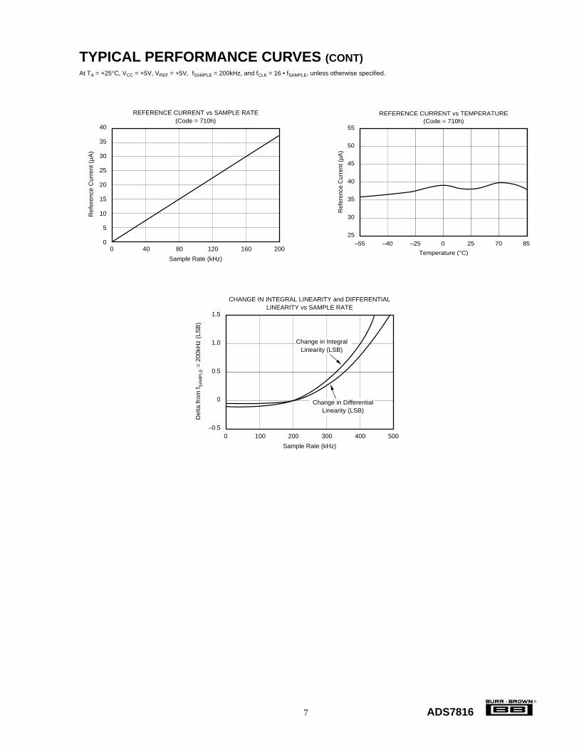
The reference current diminishes directly with both conver-sion rate and reference voltage. As the current from thereference is drawn on each bit decision, clocking the con-verter more quickly during a given conversion period willnot reduce the overall current drain from the reference. Thereference current changes only slightly with temperature.See the curves, “Reference Current vs Sample Rate” and“Reference Current vs Temperature” in the Typical Perfor-mance Curves section for more information.
DIGITAL INTERFACESERIAL INTERFACE
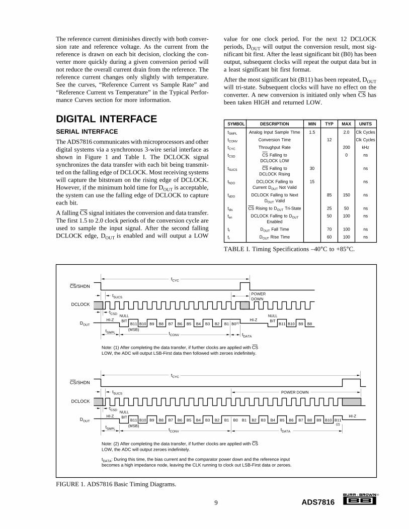
The ADS7816 communicates with microprocessors and otherdigital systems via a synchronous 3-wire serial interface asshown in Figure 1 and Table I. The DCLOCK signalsynchronizes the data transfer with each bit being transmit-ted on the falling edge of DCLOCK. Most receiving systemswill capture the bitstream on the rising edge of DCLOCK.However, if the minimum hold time for DOUT is acceptable,the system can use the falling edge of DCLOCK to captureeach bit.
A falling CS signal initiates the conversion and data transfer.The first 1.5 to 2.0 clock periods of the conversion cycle areused to sample the input signal. After the second fallingDCLOCK edge, DOUT is enabled and will output a LOW
FIGURE 1. ADS7816 Basic Timing Diagrams.
TABLE I. Timing Specifications –40°C to +85°C.
CS/SHDN
DOUT
DCLOCK
tDATA
tSUCS
tCSD
tCYC
tCONV
POWER DOWN
tSMPL
Note: (1) After completing the data transfer, if further clocks are applied with CS LOW, the ADC will output LSB-First data then followed with zeroes indefinitely.
B11
(MSB)
B10 B9 B8 B7 B6 B5 B4 B3 B2 B1 B0(1)
NULL BIT HI-ZHI-Z
B11 B10 B9 B8
NULL BIT
CS/SHDN
DOUT
DCLOCK
tCONV tDATA
tSUCS
tCYC
POWER DOWN
tSMPL
Note: (2) After completing the data transfer, if further clocks are applied with CS LOW, the ADC will output zeroes indefinitely. tDATA: During this time, the bias current and the comparator power down and the reference input becomes a high impedance node, leaving the CLK running to clock out LSB-First data or zeroes.
B11
(MSB)
B10 B9 B8 B7 B6 B5 B4 B4B3 B3B2 B2B1 B1B0
NULL BITHI-Z HI-Z
B5 B6 B7 B8 B9 B10 B11 (2)
tCSD

10
®
ADS7816
DOUT
1.4V
Test Point
3kΩ
100pF CLOAD
tr
DOUT
VOH
VOL
tf
tdDO
thDO
DOUT
DCLOCK
VOH
VOL
VIL
DOUT
Test Point
tdis Waveform 2, ten
tdis Waveform 1100pF CLOAD
3kΩ
tdis
CS/SHDN
DOUT Waveform 1(1)
DOUT Waveform 2(2)
90%
10%
VIH
1
B11
2
ten
CS/SHDN
DCLOCK
VOLDOUT
VCC
Load Circuit for tdDO, tr, and tf Voltage Waveforms for DOUT Rise and Fall TImes tr, and tf
Voltage Waveforms for DOUT Delay Times, tdDO Load Circuit for tdis and tden
Voltage Waveforms for ten
FIGURE 2. Timing Diagrams and Test Circuits for the Parameters in Table I.
Voltage Waveforms for tdis
DESCRIPTION ANALOG VALUE
Full Scale Range VREF
Least Significant VREF/4096Bit (LSB)
Full Scale VREF –1 LSB 1111 1111 1111 FFF
Midscale VREF/2 1000 0000 0000 800
Midscale – 1 LSB VREF/2 – 1 LSB 0111 1111 1111 7FF
Zero 0V 0000 0000 0000 000
Table II. Ideal Input Voltages and Output Codes.
DIGITAL OUTPUT:STRAIGHT BINARY
BINARY CODE HEX CODE
NOTES: (1) Waveform 1 is for an output with internal conditions such thatthe output is HIGH unless disabled by the output control. (2) Waveform 2is for an output with internal conditions such that the output is LOW unlessdisabled by the output control.
DATA FORMAT
The output data from the ADS7816 is in Straight Binaryformat as shown in Table II. This table represents the idealoutput code for the given input voltage and does not includethe effects of offset, gain error, or noise.
POWER DISSIPATIONThe architecture of the converter, the semiconductor fabrica-tion process, and a careful design allow the ADS7816 toconvert at up to a 200kHz rate while requiring very littlepower. Still, for the absolute lowest power dissipation, thereare several things to keep in mind.
The power dissipation of the ADS7816 scales directly withconversion rate. The first step to achieving the lowest powerdissipation is to find the lowest conversion rate that willsatisfy the requirements of the system.
In addition, the ADS7816 is in power down mode under twoconditions: when the conversion is complete and wheneverCS is HIGH (see Figure 1). Ideally, each conversion shouldoccur as quickly as possible, preferably, at a 3.2MHz clockrate. This way, the converter spends the longest possibletime in the power down mode. This is very important as the
11
®
ADS7816
converter not only uses power on each DCLOCK transition(as is typical for digital CMOS components) but also usessome current for the analog circuitry, such as the compara-tor. The analog section dissipates power continuously, untilthe power down mode is entered.
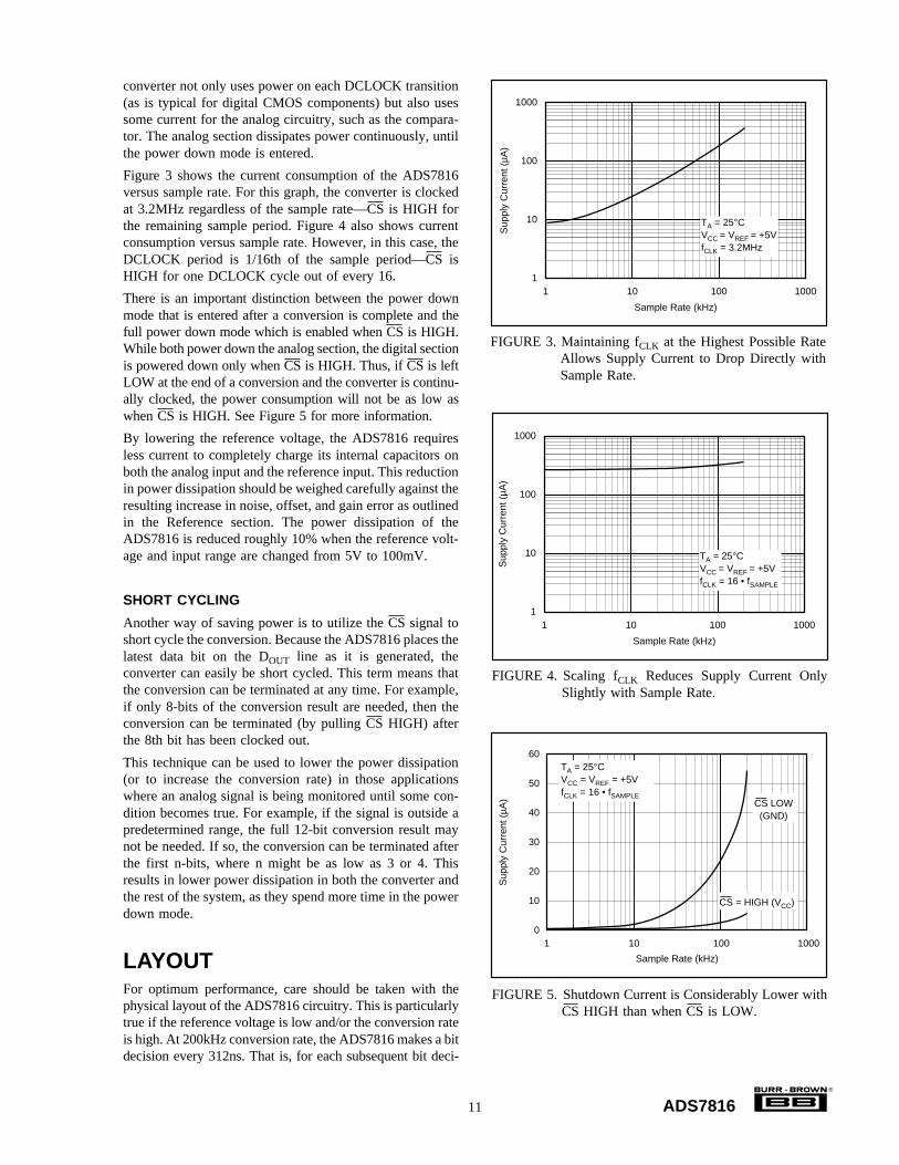
Figure 3 shows the current consumption of the ADS7816versus sample rate. For this graph, the converter is clockedat 3.2MHz regardless of the sample rate—CS is HIGH forthe remaining sample period. Figure 4 also shows currentconsumption versus sample rate. However, in this case, theDCLOCK period is 1/16th of the sample period—CS isHIGH for one DCLOCK cycle out of every 16.
There is an important distinction between the power downmode that is entered after a conversion is complete and thefull power down mode which is enabled when CS is HIGH.While both power down the analog section, the digital sectionis powered down only when CS is HIGH. Thus, if CS is leftLOW at the end of a conversion and the converter is continu-ally clocked, the power consumption will not be as low aswhen CS is HIGH. See Figure 5 for more information.
By lowering the reference voltage, the ADS7816 requiresless current to completely charge its internal capacitors onboth the analog input and the reference input. This reductionin power dissipation should be weighed carefully against theresulting increase in noise, offset, and gain error as outlinedin the Reference section. The power dissipation of theADS7816 is reduced roughly 10% when the reference volt-age and input range are changed from 5V to 100mV.
SHORT CYCLING
Another way of saving power is to utilize the CS signal toshort cycle the conversion. Because the ADS7816 places thelatest data bit on the DOUT line as it is generated, theconverter can easily be short cycled. This term means thatthe conversion can be terminated at any time. For example,if only 8-bits of the conversion result are needed, then theconversion can be terminated (by pulling CS HIGH) afterthe 8th bit has been clocked out.
This technique can be used to lower the power dissipation(or to increase the conversion rate) in those applicationswhere an analog signal is being monitored until some con-dition becomes true. For example, if the signal is outside apredetermined range, the full 12-bit conversion result maynot be needed. If so, the conversion can be terminated afterthe first n-bits, where n might be as low as 3 or 4. Thisresults in lower power dissipation in both the converter andthe rest of the system, as they spend more time in the powerdown mode.
LAYOUTFor optimum performance, care should be taken with thephysical layout of the ADS7816 circuitry. This is particularlytrue if the reference voltage is low and/or the conversion rateis high. At 200kHz conversion rate, the ADS7816 makes a bitdecision every 312ns. That is, for each subsequent bit deci-
1000
100
10
1
Sup
ply
Cur
rent
(µA
)
1 10 100 1000
Sample Rate (kHz)
TA = 25°C VCC = VREF = +5V fCLK = 3.2MHz
FIGURE 3. Maintaining fCLK at the Highest Possible RateAllows Supply Current to Drop Directly withSample Rate.
1000
100
10
1
Sup
ply
Cur
rent
(µA
)
1 10 100 1000
Sample Rate (kHz)
TA = 25°C VCC = VREF = +5V fCLK = 16 • fSAMPLE
FIGURE 4. Scaling fCLK Reduces Supply Current OnlySlightly with Sample Rate.
FIGURE 5. Shutdown Current is Considerably Lower withCS HIGH than when CS is LOW.
60
50
40
30
20
10
0
Sup
ply
Cur
rent
(µA
)
1 10 100 1000
Sample Rate (kHz)
TA = 25°C VCC = VREF = +5V fCLK = 16 • fSAMPLE
CS LOW (GND)
CS = HIGH (VCC)

12
®
ADS7816
sion, the digital output must be updated with the results of thelast bit decision, the capacitor array appropriately switchedand charged, and the input to the comparator settled to a12-bit level all within one clock cycle.
The basic SAR architecture is sensitive to spikes on thepower supply, reference, and ground connections that occurjust prior to latching the comparator output. Thus, duringany single conversion for an n-bit SAR converter, there aren “windows” in which large external transient voltages caneasily affect the conversion result. Such spikes might origi-nate from switching power supplies, digital logic, and highpower devices, to name a few. This particular source of errorcan be very difficult to track down if the glitch is almostsynchronous to the converter’s DCLOCK signal—as thephase difference between the two changes with time andtemperature, causing sporadic misoperation.
With this in mind, power to the ADS7816 should be cleanand well bypassed. A 0.1µF ceramic bypass capacitor shouldbe placed as close to the ADS7816 package as possible. Inaddition, a 1 to 10µF capacitor and a 10Ω series resistor maybe used to lowpass filter a noisy supply.
The reference should be similarly bypassed with a 0.1µFcapacitor. Again, a series resistor and large capacitor can beused to lowpass filter the reference voltage. If the referencevoltage originates from an op amp, be careful that the op-amp can drive the bypass capacitor without oscillation (theseries resistor can help in this case). Keep in mind that whilethe ADS7816 draws very little current from the reference onaverage, there are higher instantaneous current demandsplaced on the external reference circuitry.
Also, keep in mind that the ADS7816 offers no inherentrejection of noise or voltage variation in regards to thereference input. This is of particular concern when thereference input is tied to the power supply. Any noise andripple from the supply will appear directly in the digitalresults. While high frequency noise can be filtered out as
ADS7816
µP
DCLOCK
DOUT
CS/SHDNA0
A1
U3
U4
U1
U2
Thermocouple
ISO Thermal Block
MUX
OPA2370.3V
0.4V
0.2V
0.1V
+5V
R2 59kΩ
R4 1kΩ
R3 500kΩ
R5 500Ω
R7 10Ω
C3 0.1µF
C4 10µF C5
0.1µF
R6 1MΩ
R1 150kΩD1
TC2
TC1
TC3
+5V
C2 0.1µF
C1 10µF
+5VR8
46kΩ
R9 1kΩ
R10 1kΩ
R11 1kΩ
R12 1kΩ
VREF
3-Wire Interface
FIGURE 6. Thermocouple Application Using a MUX to Scale the Input Range of the ADS7816.
described in the previous paragraph, voltage variation due tothe line frequency (50Hz or 60Hz), can be difficult toremove.
The GND pin on the ADS7816 should be placed on a cleanground point. In many cases, this will be the “analog”ground. Avoid connecting the GND pin too close to thegrounding point for a microprocessor, microcontroller, ordigital signal processor. If needed, run a ground trace di-rectly from the converter to the power supply connectionpoint. The ideal layout will include an analog ground planefor the converter and associated analog circuitry.
The –In input pin should be connected directly to ground. Inthose cases where the ADS7816 is a large distance from thesignal source and/or the circuit environment contains largeEMI or RFI sources, the –In input should be connected to theground nearest the signal source. This should be done witha signal trace that is adjacent to the +In input trace. Ifappropriate, coax cable or twisted-pair wire can be used.
APPLICATION CIRCUITSFigures 6, 7, and 8 show some typical application circuits forthe ADS7816. Figure 6 uses an ADS7816 and a multiplexerto provide for a flexible data acquisition circuit. A resistorstring provides for various voltages at the multiplexer input.The selected voltage is buffered and driven into VREF. Asshown in Figure 6, the input range of the ADS7816 isprogrammable to 100mV, 200mV, 300mV, or 400mV. The100mV range would be useful for sensors such as thethermocouple shown.
Figure 7 is more complex variation of Figure 6 with in-creased flexibility. In this circuit, a digital signal processordesigned for audio applications is put to use in running threeADS7816s and a DAC56. The DAC56 provides a variablevoltage for VREF—enabling the input range of the ADS7816sto be programmed from 100mV to 3V.

13
®
ADS7816
The ADS7816s and the DSP56004 can all be placed into apower down mode. Or, the DSP56004 can run the ADS7816sat a full 3.2MHz clock rate while on-board software enablesthe ADS7816s as needed. With additional glue logic, theDSP56004 could be used to run multiple DAC56s or provideCS controls for each of the three ADS7816s.
FIGURE 7. Flexible Data Acquisition System.
Figure 8 shows a basic data acquisition system. The ADS7816input range is 0V to 5V, as the reference input is connecteddirectly to the +5V supply. The 5Ω to 10Ω resistor and 1µFto 10µF capacitor filter the microcontroller “noise” on thesupply, as well as any high-frequency noise from the supplyitself. The exact values should be picked such that the filterprovides adequate rejection of the noise.
FIGURE 8. Basic Data Acquisition System.
ADS7816
VCC
CS
DOUT
DCLOCK
VREF
+In
–In
GND
+
+
5Ω to 10Ω
1µF to 10µF
1µF to 10µF
0.1µF
Microcontroller
+5V
ADS7816
DSP56004
WST
SDO0
SDO1
SDO2
SCKT
SCKR
SDI0
SDI1
WSR
SCK/SCL
MISO/SDA
MOSI/HA0
HREQ
SS/HA2
CS
DOUT
DCLOCK
VREF
+In
–In
Serial Audio Interface
Serial Host Interface
ADS7816
CS
DOUT
DCLOCK
VREF
+In
–In
ADS7816
DAC56
CS
DOUT
DCLOCK
VREF
+In
–In
LE
CLK
DATA
VOUT
+10µF 0.1µF
+10µF 0.1µF
+10µF 0.1µF
10Ω 10Ω 10Ω

PACKAGE OPTION ADDENDUM
www.ti.com 10-Jun-2014
Addendum-Page 1
PACKAGING INFORMATION
Orderable Device Status(1)
Package Type PackageDrawing
Pins PackageQty
Eco Plan(2)
Lead/Ball Finish(6)
MSL Peak Temp(3)
Op Temp (°C) Device Marking(4/5)
Samples
ADS7816E/250 ACTIVE VSSOP DGK 8 250 Green (RoHS& no Sb/Br)
CU NIPDAUAG Level-2-260C-1 YEAR -40 to 85 A16
ADS7816E/250G4 ACTIVE VSSOP DGK 8 250 Green (RoHS& no Sb/Br)
CU NIPDAUAG Level-2-260C-1 YEAR -40 to 85 A16
ADS7816E/2K5 ACTIVE VSSOP DGK 8 2500 Green (RoHS& no Sb/Br)
CU NIPDAUAG Level-2-260C-1 YEAR -40 to 85 A16
ADS7816E/2K5G4 ACTIVE VSSOP DGK 8 2500 Green (RoHS& no Sb/Br)
CU NIPDAUAG Level-2-260C-1 YEAR -40 to 85 A16
ADS7816EB/250 ACTIVE VSSOP DGK 8 250 Green (RoHS& no Sb/Br)
CU NIPDAUAG Level-2-260C-1 YEAR -40 to 85 A16
ADS7816EB/250G4 ACTIVE VSSOP DGK 8 250 Green (RoHS& no Sb/Br)
CU NIPDAUAG Level-2-260C-1 YEAR -40 to 85 A16
ADS7816EB/2K5 ACTIVE VSSOP DGK 8 2500 Green (RoHS& no Sb/Br)
CU NIPDAUAG Level-2-260C-1 YEAR -40 to 85 A16
ADS7816EB/2K5G4 ACTIVE VSSOP DGK 8 2500 Green (RoHS& no Sb/Br)
CU NIPDAUAG Level-2-260C-1 YEAR -40 to 85 A16
ADS7816EC/250 ACTIVE VSSOP DGK 8 250 Green (RoHS& no Sb/Br)
CU NIPDAUAG Level-2-260C-1 YEAR -40 to 85 A16
ADS7816EC/250G4 ACTIVE VSSOP DGK 8 250 Green (RoHS& no Sb/Br)
CU NIPDAUAG Level-2-260C-1 YEAR -40 to 85 A16
ADS7816EC/2K5 ACTIVE VSSOP DGK 8 2500 Green (RoHS& no Sb/Br)
CU NIPDAUAG Level-2-260C-1 YEAR -40 to 85 A16
ADS7816P ACTIVE PDIP P 8 50 Green (RoHS& no Sb/Br)
CU NIPDAU N / A for Pkg Type -40 to 85 ADS7816P
ADS7816PB ACTIVE PDIP P 8 50 Green (RoHS& no Sb/Br)
CU NIPDAU N / A for Pkg Type -40 to 85 ADS7816PB
ADS7816PBG4 ACTIVE PDIP P 8 50 Green (RoHS& no Sb/Br)
CU NIPDAU N / A for Pkg Type -40 to 85 ADS7816PB
ADS7816PC ACTIVE PDIP P 8 50 Green (RoHS& no Sb/Br)
CU NIPDAU N / A for Pkg Type -40 to 85 ADS7816PC
ADS7816PCG4 ACTIVE PDIP P 8 50 Green (RoHS& no Sb/Br)
CU NIPDAU N / A for Pkg Type -40 to 85 ADS7816PC
ADS7816PG4 ACTIVE PDIP P 8 50 Green (RoHS& no Sb/Br)
CU NIPDAU N / A for Pkg Type -40 to 85 ADS7816P

PACKAGE OPTION ADDENDUM
www.ti.com 10-Jun-2014
Addendum-Page 2
Orderable Device Status(1)
Package Type PackageDrawing
Pins PackageQty
Eco Plan(2)
Lead/Ball Finish(6)
MSL Peak Temp(3)
Op Temp (°C) Device Marking(4/5)
Samples
ADS7816U ACTIVE SOIC D 8 75 Green (RoHS& no Sb/Br)
CU NIPDAU Level-2-260C-1 YEAR -40 to 85 ADS7816U
ADS7816U/2K5 ACTIVE SOIC D 8 2500 Green (RoHS& no Sb/Br)
CU NIPDAU Level-2-260C-1 YEAR -40 to 85 ADS7816U
ADS7816U/2K5G4 ACTIVE SOIC D 8 2500 Green (RoHS& no Sb/Br)
CU NIPDAU Level-2-260C-1 YEAR -40 to 85 ADS7816U
ADS7816UB ACTIVE SOIC D 8 75 Green (RoHS& no Sb/Br)
CU NIPDAU Level-2-260C-1 YEAR -40 to 85 ADS7816UB
ADS7816UB/2K5 ACTIVE SOIC D 8 2500 Green (RoHS& no Sb/Br)
CU NIPDAU Level-2-260C-1 YEAR -40 to 85 ADS7816UB
ADS7816UB/2K5G4 ACTIVE SOIC D 8 2500 Green (RoHS& no Sb/Br)
CU NIPDAU Level-2-260C-1 YEAR -40 to 85 ADS7816UB
ADS7816UBG4 ACTIVE SOIC D 8 75 Green (RoHS& no Sb/Br)
CU NIPDAU Level-2-260C-1 YEAR -40 to 85 ADS7816UB
ADS7816UC ACTIVE SOIC D 8 75 Green (RoHS& no Sb/Br)
CU NIPDAU Level-2-260C-1 YEAR -40 to 85 ADS7816UC
ADS7816UC/2K5 ACTIVE SOIC D 8 2500 Green (RoHS& no Sb/Br)
CU NIPDAU Level-2-260C-1 YEAR -40 to 85 ADS7816UC
ADS7816UC/2K5G4 ACTIVE SOIC D 8 2500 Green (RoHS& no Sb/Br)
CU NIPDAU Level-2-260C-1 YEAR -40 to 85 ADS7816UC
ADS7816UCG4 ACTIVE SOIC D 8 75 Green (RoHS& no Sb/Br)
CU NIPDAU Level-2-260C-1 YEAR -40 to 85 ADS7816UC
ADS7816UG4 ACTIVE SOIC D 8 75 Green (RoHS& no Sb/Br)
CU NIPDAU Level-2-260C-1 YEAR -40 to 85 ADS7816U
(1) The marketing status values are defined as follows:ACTIVE: Product device recommended for new designs.LIFEBUY: TI has announced that the device will be discontinued, and a lifetime-buy period is in effect.NRND: Not recommended for new designs. Device is in production to support existing customers, but TI does not recommend using this part in a new design.PREVIEW: Device has been announced but is not in production. Samples may or may not be available.
PACKAGE OPTION ADDENDUM
www.ti.com 10-Jun-2014
Addendum-Page 3
OBSOLETE: TI has discontinued the production of the device.
(2) Eco Plan - The planned eco-friendly classification: Pb-Free (RoHS), Pb-Free (RoHS Exempt), or Green (RoHS & no Sb/Br) - please check http://www.ti.com/productcontent for the latest availabilityinformation and additional product content details.TBD: The Pb-Free/Green conversion plan has not been defined.Pb-Free (RoHS): TI's terms "Lead-Free" or "Pb-Free" mean semiconductor products that are compatible with the current RoHS requirements for all 6 substances, including the requirement thatlead not exceed 0.1% by weight in homogeneous materials. Where designed to be soldered at high temperatures, TI Pb-Free products are suitable for use in specified lead-free processes.Pb-Free (RoHS Exempt): This component has a RoHS exemption for either 1) lead-based flip-chip solder bumps used between the die and package, or 2) lead-based die adhesive used betweenthe die and leadframe. The component is otherwise considered Pb-Free (RoHS compatible) as defined above.Green (RoHS & no Sb/Br): TI defines "Green" to mean Pb-Free (RoHS compatible), and free of Bromine (Br) and Antimony (Sb) based flame retardants (Br or Sb do not exceed 0.1% by weightin homogeneous material)
(3) MSL, Peak Temp. - The Moisture Sensitivity Level rating according to the JEDEC industry standard classifications, and peak solder temperature.
(4) There may be additional marking, which relates to the logo, the lot trace code information, or the environmental category on the device.
(5) Multiple Device Markings will be inside parentheses. Only one Device Marking contained in parentheses and separated by a "~" will appear on a device. If a line is indented then it is a continuationof the previous line and the two combined represent the entire Device Marking for that device.
(6) Lead/Ball Finish - Orderable Devices may have multiple material finish options. Finish options are separated by a vertical ruled line. Lead/Ball Finish values may wrap to two lines if the finishvalue exceeds the maximum column width.
Important Information and Disclaimer:The information provided on this page represents TI's knowledge and belief as of the date that it is provided. TI bases its knowledge and belief on informationprovided by third parties, and makes no representation or warranty as to the accuracy of such information. Efforts are underway to better integrate information from third parties. TI has taken andcontinues to take reasonable steps to provide representative and accurate information but may not have conducted destructive testing or chemical analysis on incoming materials and chemicals.TI and TI suppliers consider certain information to be proprietary, and thus CAS numbers and other limited information may not be available for release.
In no event shall TI's liability arising out of such information exceed the total purchase price of the TI part(s) at issue in this document sold by TI to Customer on an annual basis.
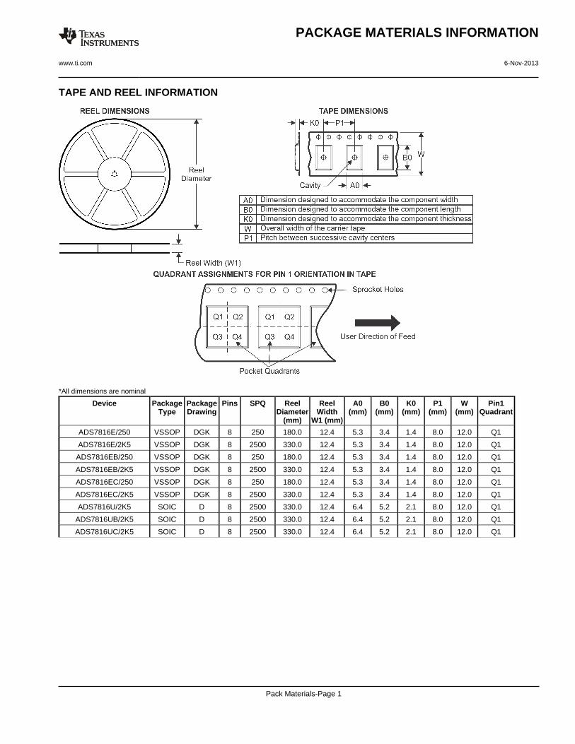
TAPE AND REEL INFORMATION
*All dimensions are nominal
Device PackageType
PackageDrawing
Pins SPQ ReelDiameter
(mm)
ReelWidth
W1 (mm)
A0(mm)
B0(mm)
K0(mm)
P1(mm)
W(mm)
Pin1Quadrant
ADS7816E/250 VSSOP DGK 8 250 180.0 12.4 5.3 3.4 1.4 8.0 12.0 Q1
ADS7816E/2K5 VSSOP DGK 8 2500 330.0 12.4 5.3 3.4 1.4 8.0 12.0 Q1
ADS7816EB/250 VSSOP DGK 8 250 180.0 12.4 5.3 3.4 1.4 8.0 12.0 Q1
ADS7816EB/2K5 VSSOP DGK 8 2500 330.0 12.4 5.3 3.4 1.4 8.0 12.0 Q1
ADS7816EC/250 VSSOP DGK 8 250 180.0 12.4 5.3 3.4 1.4 8.0 12.0 Q1
ADS7816EC/2K5 VSSOP DGK 8 2500 330.0 12.4 5.3 3.4 1.4 8.0 12.0 Q1
ADS7816U/2K5 SOIC D 8 2500 330.0 12.4 6.4 5.2 2.1 8.0 12.0 Q1
ADS7816UB/2K5 SOIC D 8 2500 330.0 12.4 6.4 5.2 2.1 8.0 12.0 Q1
ADS7816UC/2K5 SOIC D 8 2500 330.0 12.4 6.4 5.2 2.1 8.0 12.0 Q1
PACKAGE MATERIALS INFORMATION
www.ti.com 6-Nov-2013
Pack Materials-Page 1
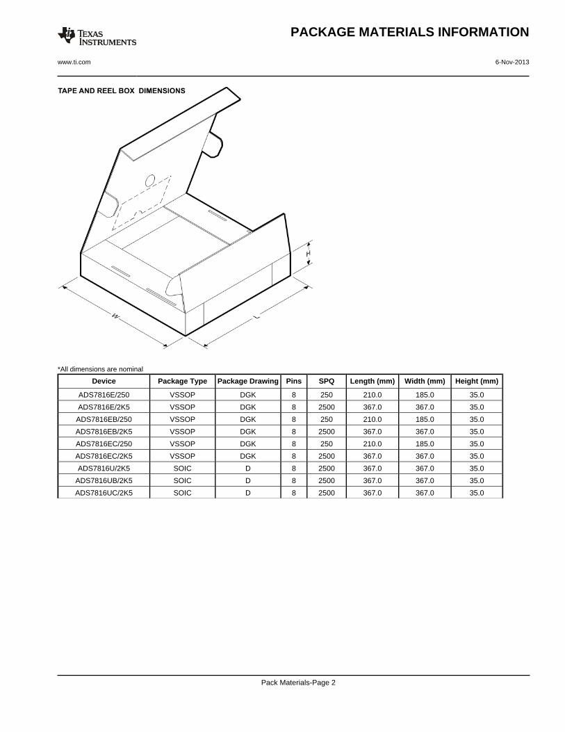
*All dimensions are nominal
Device Package Type Package Drawing Pins SPQ Length (mm) Width (mm) Height (mm)
ADS7816E/250 VSSOP DGK 8 250 210.0 185.0 35.0
ADS7816E/2K5 VSSOP DGK 8 2500 367.0 367.0 35.0
ADS7816EB/250 VSSOP DGK 8 250 210.0 185.0 35.0
ADS7816EB/2K5 VSSOP DGK 8 2500 367.0 367.0 35.0
ADS7816EC/250 VSSOP DGK 8 250 210.0 185.0 35.0
ADS7816EC/2K5 VSSOP DGK 8 2500 367.0 367.0 35.0
ADS7816U/2K5 SOIC D 8 2500 367.0 367.0 35.0
ADS7816UB/2K5 SOIC D 8 2500 367.0 367.0 35.0
ADS7816UC/2K5 SOIC D 8 2500 367.0 367.0 35.0
PACKAGE MATERIALS INFORMATION
www.ti.com 6-Nov-2013
Pack Materials-Page 2


IMPORTANT NOTICETexas Instruments Incorporated and its subsidiaries (TI) reserve the right to make corrections, enhancements, improvements and otherchanges to its semiconductor products and services per JESD46, latest issue, and to discontinue any product or service per JESD48, latestissue. Buyers should obtain the latest relevant information before placing orders and should verify that such information is current andcomplete. All semiconductor products (also referred to herein as “components”) are sold subject to TI’s terms and conditions of salesupplied at the time of order acknowledgment.TI warrants performance of its components to the specifications applicable at the time of sale, in accordance with the warranty in TI’s termsand conditions of sale of semiconductor products. Testing and other quality control techniques are used to the extent TI deems necessaryto support this warranty. Except where mandated by applicable law, testing of all parameters of each component is not necessarilyperformed.TI assumes no liability for applications assistance or the design of Buyers’ products. Buyers are responsible for their products andapplications using TI components. To minimize the risks associated with Buyers’ products and applications, Buyers should provideadequate design and operating safeguards.TI does not warrant or represent that any license, either express or implied, is granted under any patent right, copyright, mask work right, orother intellectual property right relating to any combination, machine, or process in which TI components or services are used. Informationpublished by TI regarding third-party products or services does not constitute a license to use such products or services or a warranty orendorsement thereof. Use of such information may require a license from a third party under the patents or other intellectual property of thethird party, or a license from TI under the patents or other intellectual property of TI.Reproduction of significant portions of TI information in TI data books or data sheets is permissible only if reproduction is without alterationand is accompanied by all associated warranties, conditions, limitations, and notices. TI is not responsible or liable for such altereddocumentation. Information of third parties may be subject to additional restrictions.Resale of TI components or services with statements different from or beyond the parameters stated by TI for that component or servicevoids all express and any implied warranties for the associated TI component or service and is an unfair and deceptive business practice.TI is not responsible or liable for any such statements.Buyer acknowledges and agrees that it is solely responsible for compliance with all legal, regulatory and safety-related requirementsconcerning its products, and any use of TI components in its applications, notwithstanding any applications-related information or supportthat may be provided by TI. Buyer represents and agrees that it has all the necessary expertise to create and implement safeguards whichanticipate dangerous consequences of failures, monitor failures and their consequences, lessen the likelihood of failures that might causeharm and take appropriate remedial actions. Buyer will fully indemnify TI and its representatives against any damages arising out of the useof any TI components in safety-critical applications.In some cases, TI components may be promoted specifically to facilitate safety-related applications. With such components, TI’s goal is tohelp enable customers to design and create their own end-product solutions that meet applicable functional safety standards andrequirements. Nonetheless, such components are subject to these terms.No TI components are authorized for use in FDA Class III (or similar life-critical medical equipment) unless authorized officers of the partieshave executed a special agreement specifically governing such use.Only those TI components which TI has specifically designated as military grade or “enhanced plastic” are designed and intended for use inmilitary/aerospace applications or environments. Buyer acknowledges and agrees that any military or aerospace use of TI componentswhich have not been so designated is solely at the Buyer's risk, and that Buyer is solely responsible for compliance with all legal andregulatory requirements in connection with such use.TI has specifically designated certain components as meeting ISO/TS16949 requirements, mainly for automotive use. In any case of use ofnon-designated products, TI will not be responsible for any failure to meet ISO/TS16949.Products ApplicationsAudio www.ti.com/audio Automotive and Transportation www.ti.com/automotiveAmplifiers amplifier.ti.com Communications and Telecom www.ti.com/communicationsData Converters dataconverter.ti.com Computers and Peripherals www.ti.com/computersDLP® Products www.dlp.com Consumer Electronics www.ti.com/consumer-appsDSP dsp.ti.com Energy and Lighting www.ti.com/energyClocks and Timers www.ti.com/clocks Industrial www.ti.com/industrialInterface interface.ti.com Medical www.ti.com/medicalLogic logic.ti.com Security www.ti.com/securityPower Mgmt power.ti.com Space, Avionics and Defense www.ti.com/space-avionics-defenseMicrocontrollers microcontroller.ti.com Video and Imaging www.ti.com/videoRFID www.ti-rfid.comOMAP Applications Processors www.ti.com/omap TI E2E Community e2e.ti.comWireless Connectivity www.ti.com/wirelessconnectivity
Mailing Address: Texas Instruments, Post Office Box 655303, Dallas, Texas 75265Copyright © 2014, Texas Instruments Incorporated