12-Bit, 53MHz Sampling ANALOG-TO-DIGITAL CONVERTER
24
12-Bit, 53MHz Sampling ANALOG-TO-DIGITAL CONVERTER FEATURES ● SPURIOUS-FREE DYNAMIC RANGE: 82dB at 10MHz f IN ● HIGH SNR: 67.5dB (2Vp-p), 69dB (3Vp-p) ● LOW POWER: 335mW ● INTERNAL OR EXTERNAL REFERENCE ● LOW DNL: 0.5LSB ● FLEXIBLE INPUT RANGE: 2Vp-p to 3Vp-p ● SSOP-28 PACKAGE DESCRIPTION The ADS807 is a high-speed, high dynamic range, 12-bit pipelined Analog-to-Digital (A/D) converter. This con- verter includes a high-bandwidth track-and-hold that gives excellent spurious performance up to and beyond the Nyquist rate. The differential nature of this track-and-hold and A/D converter circuitry minimizes even-order harmonics and gives excellent common-mode noise immunity. The track-and-hold can also be operated single-ended. The ADS807 provides for setting the full-scale range of the converter without any external reference circuitry. The inter- nal reference can be disabled allowing low drive, internal references to be used for improved tracking in multichannel systems. The ADS807 provides an over-range indicator flag to indicate an input signal that exceeds the full-scale input range of the converter. This flag can be used to reduce the gain of front end gain control circuitry. There is also an output enable pin to allow for multiplexing and testability on a PC board. The ADS807 employs digital error correction techniques to provide excellent differential linearity for demanding imaging applications. APPLICATIONS ● COMMUNICATIONS IF PROCESSING ● COMMUNICATIONS BASESTATIONS ● TEST EQUIPMENT ● MEDICAL IMAGING ● VIDEO DIGITIZING ● CCD DIGITIZING ADS807E Pipelined A/D Converter Internal Reference Optional External Reference Timing Circuitry Error Correction Logic 3-State Outputs T/H D0 • • • D11 CLK ADS807 OE IN INT/EXT IN CM +2.5V +2.5V +3V +2V +2V +3V FS SEL (Opt.) ADS807 SBAS072A – JANUARY 1999 – REVISED JULY 2002 www.ti.com PRODUCTION DATA information is current as of publication date. Products conform to specifications per the terms of Texas Instruments standard warranty. Production processing does not necessarily include testing of all parameters. Copyright © 1999, Texas Instruments Incorporated Please be aware that an important notice concerning availability, standard warranty, and use in critical applications of Texas Instruments semiconductor products and disclaimers thereto appears at the end of this data sheet.
Transcript of 12-Bit, 53MHz Sampling ANALOG-TO-DIGITAL CONVERTER
12-Bit, 53MHz Sampling ANALOG-TO-DIGITAL CONVERTER
FEATURES SPURIOUS-FREE DYNAMIC RANGE:
82dB at 10MHz fIN
HIGH SNR: 67.5dB (2Vp-p), 69dB (3Vp-p)
LOW POWER: 335mW
INTERNAL OR EXTERNAL REFERENCE
LOW DNL: 0.5LSB
FLEXIBLE INPUT RANGE: 2Vp-p to 3Vp-p
SSOP-28 PACKAGE
DESCRIPTIONThe ADS807 is a high-speed, high dynamic range,12-bit pipelined Analog-to-Digital (A/D) converter. This con-verter includes a high-bandwidth track-and-hold that givesexcellent spurious performance up to and beyond the Nyquistrate. The differential nature of this track-and-hold and A/Dconverter circuitry minimizes even-order harmonics and givesexcellent common-mode noise immunity. The track-and-holdcan also be operated single-ended.
The ADS807 provides for setting the full-scale range of theconverter without any external reference circuitry. The inter-nal reference can be disabled allowing low drive, internalreferences to be used for improved tracking in multichannelsystems.
The ADS807 provides an over-range indicator flag to indicatean input signal that exceeds the full-scale input range of theconverter. This flag can be used to reduce the gain of frontend gain control circuitry. There is also an output enable pinto allow for multiplexing and testability on a PC board.
The ADS807 employs digital error correction techniques toprovide excellent differential linearity for demanding imagingapplications.
APPLICATIONS COMMUNICATIONS IF PROCESSING
COMMUNICATIONS BASESTATIONS
TEST EQUIPMENT
MEDICAL IMAGING
VIDEO DIGITIZING
CCD DIGITIZING
ADS807E
PipelinedA/D
Converter
InternalReference
Optional ExternalReference
TimingCircuitry
ErrorCorrection
Logic
3-StateOutputsT/H
D0•••
D11
CLK
ADS807
OE
IN
INT/EXT
IN
CM
+2.5V
+2.5V
+3V
+2V
+2V
+3V
FSSEL
(Opt.)
ADS807
SBAS072A – JANUARY 1999 – REVISED JULY 2002
www.ti.com
PRODUCTION DATA information is current as of publication date.Products conform to specifications per the terms of Texas Instrumentsstandard warranty. Production processing does not necessarily includetesting of all parameters.
Copyright © 1999, Texas Instruments Incorporated
Please be aware that an important notice concerning availability, standard warranty, and use in critical applications ofTexas Instruments semiconductor products and disclaimers thereto appears at the end of this data sheet.
ADS8072SBAS072Awww.ti.com
PIN DESIGNATOR DESCRIPTION
1 GND Ground2 Bit 1 Data Bit 1 (MSB)3 Bit 2 Data Bit 24 Bit 3 Data Bit 35 Bit 4 Data Bit 46 Bit 5 Data Bit 57 Bit 6 Data Bit 68 Bit 7 Data Bit 79 Bit 8 Data Bit 810 Bit 9 Data Bit 911 Bit 10 Data Bit 1012 Bit 11 Data Bit 1113 Bit 12 Data Bit 12 (LSB)14 CLK Convert Clock15 +VS +5V Supply16 FSSEL HI = 3V, LO = 2V17 OTR Out-of-Range Indicator18 INT/EXT Reference Select: HIGH or Floating = Exter-
nal LOW = Internal 50kΩ pull-up.19 OE Output Enable20 GND Ground21 REFB Bottom Reference/Bypass22 REFT Top Reference/Bypass23 CM Common-Mode Voltage Output24 IN Complementary Analog Input25 IN Analog Input26 GND Ground27 +VS +5V Supply28 VDRV Logic Driver Supply Voltage
PIN DESCRIPTIONS
+VS ....................................................................................................... +6VAnalog Input ........................................................... (–0.3V) to (+VS + 0.3V)Logic Input ............................................................. (–0.3V) to (+VS + 0.3V)Case Temperature ......................................................................... +100°CJunction Temperature .................................................................... +150°CStorage Temperature ..................................................................... +150°C
NOTE: (1) Stresses above those listed under “Absolute Maximum Ratings”may cause permanent damage to the device. Exposure to absolute maximumconditions for extended periods may affect device reliability.
ABSOLUTE MAXIMUM RATINGS(1)
Top View SSOP
PIN CONFIGURATION
ELECTROSTATICDISCHARGE SENSITIVITY
This integrated circuit can be damaged by ESD. Texas Instru-ments recommends that all integrated circuits be handled withappropriate precautions. Failure to observe proper handling andinstallation procedures can cause damage.
ESD damage can range from subtle performance degradation tocomplete device failure. Precision integrated circuits may bemore susceptible to damage because very small parametricchanges could cause the device not to meet its publishedspecifications.
GND
Bit 1 (MSB)
Bit 2
Bit 3
Bit 4
Bit 5
Bit 6
Bit 7
Bit 8
Bit 9
Bit 10
Bit 11
Bit 12 (LSB)
CLK
VDRV
+VS
GND
IN
IN
CM
REFT
REFB
GND
OE
INT/EXT
OTR
FSSEL
+VS
1
2
3
4
5
6
7
8
9
10
11
12
13
14
28
27
26
25
24
23
22
21
20
19
18
17
16
15
ADS807E
SPECIFIEDPACKAGE TEMPERATURE PACKAGE ORDERING TRANSPORT
PRODUCT PACKAGE-LEAD DESIGNATOR(1) RANGE MARKING NUMBER MEDIA, QUANTITY
ADS807E SSOP-28 DB –40°C to +85°C ADS807E ADS807E Tube, 50" " " " " ADS807E/1K Tape and Reel, 1000
NOTE: (1) For the most current specifications and package information refer to our web site at www.ti.com.
PACKAGE/ORDERING INFORMATION
ADS807 3SBAS072A www.ti.com
ADS807E
PARAMETER CONDITIONS MIN TYP MAX UNITS
RESOLUTION 12 Tested Bits
SPECIFIED TEMPERATURE RANGE Ambient Air –40 +85 °C
ANALOG INPUT2V Full-Scale Input Range (Differential) 2Vp-p, INT or EXT Ref 2 3 V2V Full-Scale Input Range (Single-Ended) 2Vp-p, INT or EXT Ref 1.5 3.5 V3V Full-Scale Input Range (Differential) 3Vp-p, INT or EXT Ref 1.75 3.25 V3V Full-Scale Input Range (Single-Ended) 3Vp-p, INT or EXT Ref 1 4 VAnalog Input Bias Current 1 µAAnalog Input Bandwidth 270 MHzInput Impedance 1.25 || 3 MΩ || pF
CONVERSION CHARACTERISTICSSample Rate 10k 53M Samples/sData Latency 6 Clock Cycles
DYNAMIC CHARACTERISTICSDifferential Linearity Error (largest code error)
f = 1MHz ±0.5 ±1.0 LSBf = 10MHz fS = 40MHz ±0.5 ±1.0 LSB
No Missing Codes fS = 50MHz,TA = +25°C TestedNo MIssing Codes fS = 40MHz, Full Temp TestedIntegral Nonlinearity Error, f = 1MHz ±2.0 ±4.0 LSBsSpurious-Free Dynamic Range(1)
f = 1MHz (–1dB input) 83 dBFS(2)
f = 10MHz (–1dB input) 67 82 dBFSf = 20MHz (–1dB input) 76 dBFSf = 40MHz (undersampling) 76 dBFSf = 1MHz to 10MHz, fS = 40MHz 2Vp-p, Single-Ended Input 62 69 dBFS
2-Tone Intermodulation Distortion(3)
f = 12MHz and 13MHz (–7dB each tone) 71 dBc
Signal-to-Noise Ratio (SNR)f = 1MHz (–1dB input) 63 68 dBf = 10MHz (–1dB input) 63 68 dBf = 20MHz (–dB input) 66 dBf = 40MHz (undersampling) 67 dBf = 1MHz to 10MHz, fS = 40MHz 63 67.5 dBf = 1MHz to 10MHz, fS = 40MHz 2Vp-p, Single-Ended Input 60 67 dB
f = 1MHz (–1dB input) 3Vp-p 69 dBf = 10MHz (–1dB input) 3Vp-p 69 dB
Signal-to-(Noise + Distortion) (SINAD)(4)
f = 1MHz (–1dBFS input) 61 67 dBf = 10MHz (–1dBFS input) 61 67 dBf = 20MHz (–1dBFS input) 67 dBf = 1MHz to 10MHz, fS = 40MHz 63 67 dBf = 1MHz to 10MHz, fS = 40MHz 2Vp-p, Single-Ended Input 60 64 dB
f = 1MHz (–1dBFS input) 3Vp-p 69 dBf = 10MHz (–dBFS Input) 3Vp-p 69 dB
Output Noise Input Grounded 0.2 LSBs rmsAperture Delay Time 2 nsAperture Jitter 1.2 ps rmsOver-Voltage Recovery Time 2 ns
DIGITAL INPUTSLogic FamilyConvert Command Start ConversionHigh Level Input Current(5) (VIN = 5V) +50 µALow Level Input Current (VIN = 0V) +10 µAHigh Level Input Voltage +2.4 VLow Level Input Voltage +1.0 VInput Capacitance 5 pF
ELECTRICAL CHARACTERISTICSAt TA = full specified temperature range, VS = +5V, differential input range = 2V to 3V for each input, sampling rate = 50MHz, unless otherwise noted.
CMOSRising Edge of Convert Clock
ADS8074SBAS072Awww.ti.com
ADS807E
PARAMETER CONDITIONS MIN TYP MAX UNITS
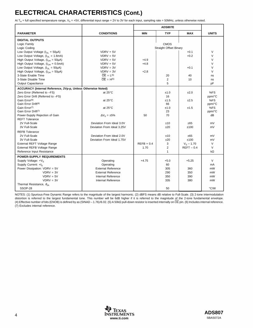
ELECTRICAL CHARACTERISTICS (Cont.)At TA = full specified temperature range, VS = +5V, differential input range = 2V to 3V for each input, sampling rate = 50MHz, unless otherwise noted.
CMOSStraight Offset Binary
DIGITAL OUTPUTSLogic FamilyLogic CodingLow Output Voltage (IOL = 50µA) VDRV = 5V +0.1 VLow Output Voltage, (IOL = 1.6mA) VDRV = 5V +0.2 VHigh Output Voltage, (IOH = 50µA) VDRV = 5V +4.9 VHigh Output Voltage, (IOH = 0.5mA) VDRV = 5V +4.8 VLow Output Voltage, (IOL = 50µA) VDRV = 3V +0.1 VHigh Output Voltage, (IOH = 50µA) VDRV = 3V +2.8 V3-State Enable Time OE = L(5) 20 40 ns3-State Disable Time OE = H(5) 2 10 nsOutput Capacitance 5 pF
ACCURACY (Internal Reference, 2Vp-p, Unless Otherwise Noted)Zero Error (Referred to –FS) at 25°C ±1.0 ±2.0 %FSZero Error Drift (Referred to –FS) 16 ppm/°CGain Error(6) at 25°C ±1.5 ±2.5 %FSGain Error Drift(6) 66 ppm/°CGain Error(7) at 25°C ±1.0 ±1.5 %FSGain Error Drift(7) 23 ppm/°CPower-Supply Rejection of Gain ∆VS = ±5% 50 70 dBREFT Tolerance
2V Full-Scale Deviation From Ideal 3.0V ±10 ±65 mV3V Full-Scale Deviation From Ideal 3.25V ±20 ±100 mV
REFB Tolerance2V Full-Scale Deviation From Ideal 2.0V ±10 ±65 mV3V Full-Scale Deviation From Ideal 1.75V ±20 ±100 mV
External REFT Voltage Range REFB + 0.4 3 VS – 1.70 VExternal REFB Voltage Range 1.70 2 REFT – 0.4 VReference Input Resistance 1 kΩ
POWER-SUPPLY REQUIREMENTSSupply Voltage: +VS Operating +4.75 +5.0 +5.25 VSupply Current: +IS Operating 60 mAPower Dissipation: VDRV = 5V External Reference 305 360 mW
VDRV = 3V External Reference 290 350 mWVDRV = 5V Internal Reference 350 390 mWVDRV = 3V Internal Reference 335 380 mW
Thermal Resistance, θJA
SSOP-28 50 °C/W
NOTES: (1) Spurious-Free Dynamic Range refers to the magnitude of the largest harmonic. (2) dBFS means dB relative to Full-Scale. (3) 2-tone intermodulationdistortion is referred to the largest fundamental tone. This number will be 6dB higher if it is referred to the magnitude of the 2-tone fundamental envelope.(4) Effective number of bits (ENOB) is defined by as (SINAD – 1.76)/6.02. (5) A 50kΩ pull-down resistor is inserted internally on OE pin. (6) Includes internal reference.(7) Excludes internal reference.
ADS807 5SBAS072A www.ti.com
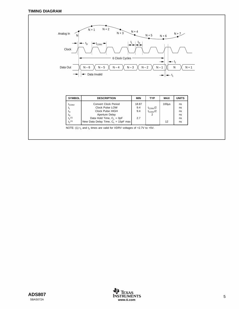
TIMING DIAGRAM
6 Clock Cycles
Data Invalid
tDtL tHtCONV
N – 6 N – 5 N – 4 N – 3 N – 2 N – 1 N N + 1Data Out
Clock
Analog InN
t2
N + 1 N + 2N + 3 N + 4
N + 5 N + 6N + 7
t1
SYMBOL DESCRIPTION MIN TYP MAX UNITS
tCONV Convert Clock Period 18.87 100µs nstL Clock Pulse LOW 9.4 tCONV/2 nstH Clock Pulse HIGH 9.4 tCONV/2 nstD Aperture Delay 2 nst1(1) Data Hold Time, CL = 0pF 2.7 nst2 (1) New Data Delay Time, CL = 15pF max 12 ns
NOTE: (1) t1 and t2 times are valid for VDRV voltages of +2.7V to +5V.
ADS8076SBAS072Awww.ti.com
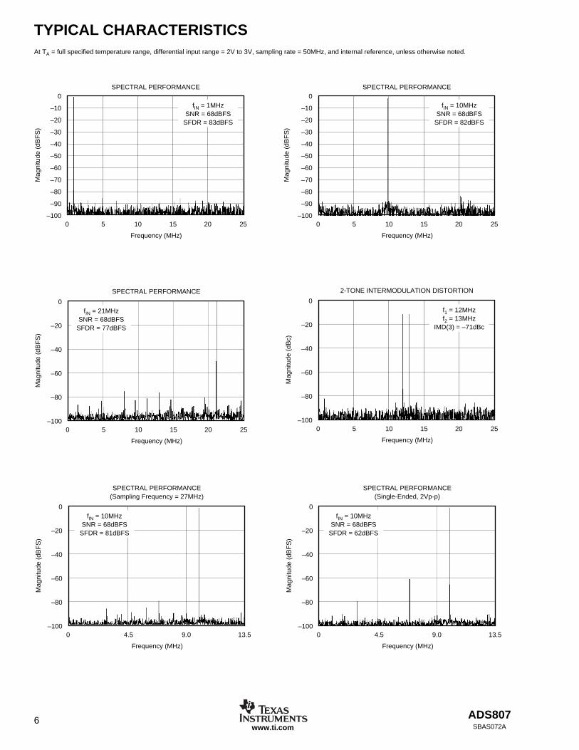
SPECTRAL PERFORMANCE
Frequency (MHz)
0 5 10 15 20 25
Mag
nitu
de (
dBF
S)
0
–20
–40
–60
–80
–100
fIN = 21MHzSNR = 68dBFS
SFDR = 77dBFS
SPECTRAL PERFORMANCE
Frequency (MHz)
0 5 10 15 20 25
Mag
nitu
de (
dBF
S)
0
–10
–20
–30
–40
–50
–60
–70
–80
–90
–100
fIN = 10MHzSNR = 68dBFS
SFDR = 82dBFS
SPECTRAL PERFORMANCE
Frequency (MHz)
0 5 10 15 20 25
Mag
nitu
de (
dBF
S)
0
–10
–20
–30
–40
–50
–60
–70
–80
–90
–100
fIN = 1MHzSNR = 68dBFS
SFDR = 83dBFS
SPECTRAL PERFORMANCE(Single-Ended, 2Vp-p)
Frequency (MHz)
0 4.5 9.0 13.5
Mag
nitu
de (
dBF
S)
0
–20
–40
–60
–80
–100
fIN = 10MHzSNR = 68dBFS
SFDR = 62dBFS
SPECTRAL PERFORMANCE(Sampling Frequency = 27MHz)
Frequency (MHz)
0 4.5 9.0 13.5
Mag
nitu
de (
dBF
S)
0
–20
–40
–60
–80
–100
fIN = 10MHzSNR = 68dBFS
SFDR = 81dBFS
TYPICAL CHARACTERISTICSAt TA = full specified temperature range, differential input range = 2V to 3V, sampling rate = 50MHz, and internal reference, unless otherwise noted.
2-TONE INTERMODULATION DISTORTION
Frequency (MHz)
0 5 10 15 20 25
Mag
nitu
de (
dBc)
0
–20
–40
–60
–80
–100
f1 = 12MHzf2 = 13MHz
IMD(3) = –71dBc
ADS807 7SBAS072A www.ti.com
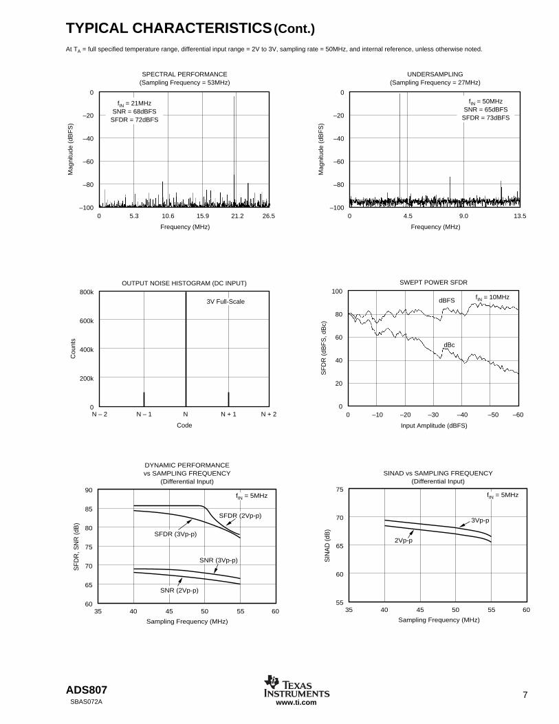
SPECTRAL PERFORMANCE(Sampling Frequency = 53MHz)
Frequency (MHz)
0 5.3 10.6 15.9 21.2 26.5
Mag
nitu
de (
dBF
S)
0
–20
–40
–60
–80
–100
fIN = 21MHzSNR = 68dBFS
SFDR = 72dBFS
SWEPT POWER SFDR
Input Amplitude (dBFS)
0 –10 –20 –30 –40 –50 –60
SF
DR
(dB
FS
, dB
c)
100
80
60
40
20
0
fIN = 10MHz
dBc
dBFS
UNDERSAMPLING(Sampling Frequency = 27MHz)
Frequency (MHz)
0 4.5 9.0 13.5
Mag
nitu
de (
dBF
S)
0
–20
–40
–60
–80
–100
fIN = 50MHzSNR = 65dBFS
SFDR = 73dBFS
TYPICAL CHARACTERISTICS (Cont.)At TA = full specified temperature range, differential input range = 2V to 3V, sampling rate = 50MHz, and internal reference, unless otherwise noted.
DYNAMIC PERFORMANCEvs SAMPLING FREQUENCY
(Differential Input)
Sampling Frequency (MHz)
SFD
R, S
NR
(dB
)
90
85
80
75
70
65
6035 40 45 50 55 60
SNR (3Vp-p)
SNR (2Vp-p)
SFDR (2Vp-p)
SFDR (3Vp-p)
fIN = 5MHz
SINAD vs SAMPLING FREQUENCY(Differential Input)
Sampling Frequency (MHz)
SIN
AD
(dB
)
75
70
65
60
5535 40 45 50 55 60
3Vp-p
2Vp-p
fIN = 5MHz
800k
600k
400k
200k
0
OUTPUT NOISE HISTOGRAM (DC INPUT)
Cou
nts
N – 2 N – 1 N N + 1 N + 2
Code
3V Full-Scale
ADS8078SBAS072Awww.ti.com
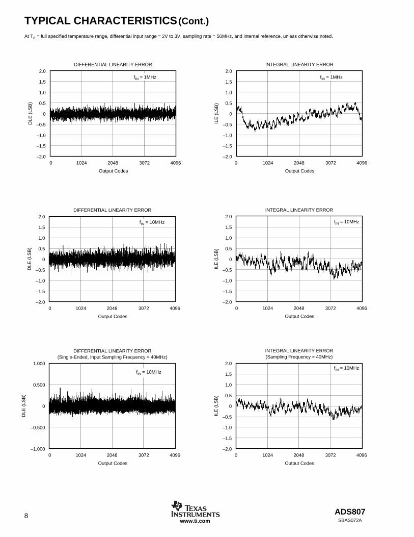
DIFFERENTIAL LINEARITY ERROR(Single-Ended, Input Sampling Frequency = 40MHz)
Output Codes
DLE
(LS
B)
1.000
0.500
0
–0.500
–1.00010240 2048 3072 4096
fIN = 10MHz
INTEGRAL LINEARITY ERROR(Sampling Frequency = 40MHz)
Output Codes
ILE
(LS
B)
2.0
1.5
1.0
0.5
0
–0.5
–1.0
–1.5
–2.010240 2048 3072 4096
fIN = 10MHz
INTEGRAL LINEARITY ERROR
Output Codes
ILE
(LS
B)
2.0
1.5
1.0
0.5
0
–0.5
–1.0
–1.5
–2.010240 2048 3072 4096
fIN = 10MHz
DIFFERENTIAL LINEARITY ERROR
Output Codes
DLE
(LS
B)
2.0
1.5
1.0
0.5
0
–0.5
–1.0
–1.5
–2.010240 2048 3072 4096
fIN = 10MHz
INTEGRAL LINEARITY ERROR
Output Codes
ILE
(LS
B)
2.0
1.5
1.0
0.5
0
–0.5
–1.0
–1.5
–2.00 1024 2048 3072 4096
fIN = 1MHz
DIFFERENTIAL LINEARITY ERROR
Output Codes
DLE
(LS
B)
2.0
1.5
1.0
0.5
0
–0.5
–1.0
–1.5
–2.010240 2048 3072 4096
fIN = 1MHz
TYPICAL CHARACTERISTICS (Cont.)At TA = full specified temperature range, differential input range = 2V to 3V, sampling rate = 50MHz, and internal reference, unless otherwise noted.
ADS807 9SBAS072A www.ti.com
• improves the noise immunity based on the converter’scommon-mode input rejection
Using the single-ended mode, the signal is applied to one ofthe inputs, while the other input is biased with a DC voltageto the required common-mode level. Both inputs are equal interms of their impedance and performance, except thatapplying the signal to the complementary input (IN) insteadof the IN input will invert the input signal relative to the outputcode. For example, in case the input driver operates ininverting mode, using IN as the signal input will restore thephase of the signal to its original orientation. Time-domainapplications may benefit from a single-ended interface con-figuration and its reduced circuit complexity. While maintain-ing good SNR, driving the ADS807 with a single-endedsignal will result in a reduction of the distortion performance.Employing dual-supply amplifiers and AC-coupling will usu-ally yield the best results, while DC-coupling and/or single-supply amplifiers impose additional design constraints due totheir headroom requirements, especially when selecting the3Vp-p input range. However, single-supply amplifiers havethe advantage of inherently limiting their output swing towithin the supply rails. Alternatively, a voltage-limiting ampli-fier, like the OPA688, may be considered to set fixed-signallimits and avoid any severe over-range condition for the A/Dconverter.
The full-scale input range of the ADS807 is defined by thereference voltages. For example, setting the range select pinto FSSEL = LOW, and using the internal references(REFT = +3.0V and REFTB = +2.0V), the full-scale range isdefined to: FSR = 2 • (REFT – REFB) = 2Vp-p.
The trade-off of the differential input configuration versus thesingle-ended is its higher complexity. In either case, theselection of the driver amplifier should be such that theamplifier’s performance will not degrade the A/D converter’sperformance. The ADS807 operates on a single powersupply, which requires a level shift to a ground-based bipolarinput signals to comply with its input voltage range require-ments.
The input of the ADS807 is of a capacitive nature and thedriving source needs to provide the current to charge ordischarge the input sampling capacitor while the track-and-hold is in track mode. This effectively results in a dynamicinput impedance which depends on the sampling frequency.It most applications, it is recommended to add a seriesresistor, typically 20Ω to 50Ω, between the drive source andthe converter inputs. This will isolate the capacitive inputfrom the source, which can be crucial to avoid gain peakingwhen using wideband operational amplifiers. Secondly, it willcreate a 1st-order, low-pass filter in conjunction with thespecified input capacitance of the ADS807. Its cutoff fre-quency can be adjusted even further by adding an externalshunt capacitor from each signal input to ground. The opti-mum values of this R-C network depend on a variety offactors which include the ADS807 sampling rate, the se-lected op amp, the interface configuration, and the particularapplication (time domain versus frequency domain). Gener-ally, increasing the size of the series resistor and/or capacitor
APPLICATION INFORMATIONTHEORY OF OPERATION
The ADS807 is a high-speed, CMOS A/D converter whichemploys a pipelined converter architecture consisting of 12internal stages. Each stage feeds its data into the digitalerror correction logic ensuring excellent differential linearityand no missing codes at the 12-bit level. The output databecomes valid after the rising clock edge (see Timing Dia-gram). The pipeline architecture results in a data latency of6 clock cycles.
The analog input of the ADS807 consists of a differentialtrack-and-hold circuit. The differential topology along withtightly matched poly-poly capacitors produce a high level ofAC performance at high sampling rates and in undersamplingapplications.
Both inputs (IN, IN) require external biasing using a com-mon-mode voltage that is typically at the mid-supply level(+VS/2).
DRIVING THE ANALOG INPUTS
The analog inputs of the ADS807 are a very high impedance.They should be driven through an R-C network designed topass the highest frequency of interest. This prevents high-frequency noise in the input from affecting SFDR and SNR.The ADS807 can be used in a wide variety of applicationsand deciding on the best performing analog interface circuitdepends on the type of application. The circuit definitionshould include considerations of input frequency spectrumand amplitude, single-ended or differential drive, and avail-able power supplies. For example, communication (frequencydomain) applications process frequency bands not includingDC. In imaging (time domain) applications, the input DCcomponent must be maintained into the A/D converter.Features of the ADS807, including full-scale select (FSSEL),external reference, and CM output provide flexibility to ac-commodate a wide range of applications. The ADS807should be configured to meet application objectives whileobserving the headroom requirements of the driving amplifi-ers to yield the best overall performance.
The ADS807 input structure allows it to be driven eithersingle-ended or differentially. Differential operation of theADS807 requires an in-phase input signal and a 180° out-of-phase part simultaneously applied to the inputs (IN, IN). Thedifferential operation offers a number of advantages which,in most applications, will be instrumental in achieving thebest dynamic performance of the ADS807:
• the signal swing is half of that required for the single-ended operation and therefore, is less demanding toachieve while maintaining good linearity performance fromthe signal source
• the reduced signal swing allows for more headroom in theinterface circuitry and therefore, a wider selection of thebest suitable driver op amp
• even-order harmonics are minimized
ADS80710SBAS072Awww.ti.com
will improve the SNR performance, but depending on thesignal source, large resistor values may be detrimental toachieving good harmonic distortion. In any case, optimizingthe R-C values for the specific application is encouraged.
Transformer Coupled, Single-Ended to DifferentialConfiguration
If the application requires a signal conversion from a single-ended source to drive the ADS807 differentially, an RFtransformer might be a good solution. The selected trans-former must have a center tap in order to apply the common-mode DC voltage necessary to bias the converter inputs. AC-grounding the center tap will generate the differential signalswing across the secondary winding. Consider a step-uptransformer to take advantage of a signal amplification with-out the introduction of another noise source. Furthermore,the reduced signal swing from the source may lead toimproved distortion performance.
The differential input configuration provides a noticeableadvantage of achieving good SFDR over a wide range ofinput frequencies. In this mode, both inputs of the ADS807see matched impedances. Figure 1 shows the schematic forthe suggested transformer coupled interface circuit. Thecomponent values of the R-C low-pass may be optimizeddepending on the desired roll-off frequency. The resistoracross the secondary side (RT) should be calculated usingthe equation RT = n2 • RG to match the source impedance(RG) for good power transfer and VSWR.
The circuit example of Figure 1 shows the voltage-feedbackamplifier OPA680 driving the RF transformer, which convertsthe single-ended signal into a differential one. The OPA680can be employed for either single- or dual-supply operation.For details on how to optimize its frequency response, referto the OPA680 data sheet (SBOS083), available atwww.ti.com. With the 49.9Ω series output resistor, the ampli-fier emulates a 50Ω source (RG). Any DC content of thesignal can be easily blocked by a capacitor (0.1µF) and toalso to avoid DC loading of the op amp’s output stage.
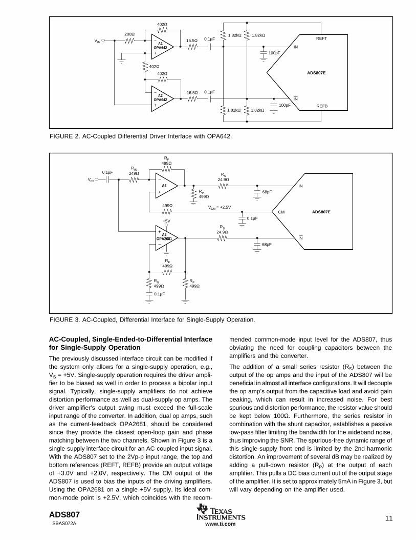
AC-Coupled, Single-Ended-to-Differential Interfacewith Dual-Supply Op Amps
Communications applications, in particular, demand a veryhigh dynamic range and low levels of intermodulation distor-tion, but usually allow the input signal to be AC-coupled intothe A/D converter. Appropriate driver amplifiers need to beselected to maintain the excellent distortion performance ofthe ADS807. Often, these op amps deliver the lowest distor-tion with a small, ground-centered signal swing that requiresdual power supplies. Because of the AC-coupling, this re-quirement can be easily accomplished and the needed levelshifting of the input signal can be implemented withoutaffecting the driver circuit.
See Figure 2 for an example of such an interface circuitspecifically designed to maximize the dynamic performance.The voltage feedback amplifier, OPA642, maintains an ex-cellent distortion performance for input frequencies of up to15MHz. The two amplifiers (A1, A2) are configured as aninverting and noninverting gain stage to convert the inputsignal from single-ended to differential. The nominal gain forthis stage is set to +2V/V. The outputs of the OPA642s areAC-coupled to the converter’s differential inputs. This willkeep the distortion performance at its best since the signalrange stays within the linear region of the op amp andsufficient headroom to the supply rails can be maintained.Four resistors located between the top (REFT) and bottom(REFB) reference shift the input signal to a common-modevoltage of approximately +2.5V.
The interface circuit of Figure 2 can be modified to extendthe bandwidth to approximately 25MHz by replacing theOPA642 with its decompensated version, the OPA643. TheOPA643 provides the necessary slew rate for a low distortionfront end to the ADS807. With a minimum gain stability of +3,the gain resistors have to be modified, as well as optimizingthe series resistor and shunt capacitance at each of theconverter inputs.
FIGURE 1. Converting a Single-Ended Input Signal into a Differential Signal Using a RF-Transformer.
VIN
IN
INCM
+2.5V
24.9Ω
24.9Ω
47pF
RT
47pF
10µF 0.1µF
1:n0.1µF
RG
R2
R1
OPA680
49.9Ω
ADS807E
+
ADS807 11SBAS072A www.ti.com
AC-Coupled, Single-Ended-to-Differential Interfacefor Single-Supply Operation
The previously discussed interface circuit can be modified ifthe system only allows for a single-supply operation, e.g.,VS = +5V. Single-supply operation requires the driver ampli-fier to be biased as well in order to process a bipolar inputsignal. Typically, single-supply amplifiers do not achievedistortion performance as well as dual-supply op amps. Thedriver amplifier’s output swing must exceed the full-scaleinput range of the converter. In addition, dual op amps, suchas the current-feedback OPA2681, should be consideredsince they provide the closest open-loop gain and phasematching between the two channels. Shown in Figure 3 is asingle-supply interface circuit for an AC-coupled input signal.With the ADS807 set to the 2Vp-p input range, the top andbottom references (REFT, REFB) provide an output voltageof +3.0V and +2.0V, respectively. The CM output of theADS807 is used to bias the inputs of the driving amplifiers.Using the OPA2681 on a single +5V supply, its ideal com-mon-mode point is +2.5V, which coincides with the recom-
mended common-mode input level for the ADS807, thusobviating the need for coupling capacitors between theamplifiers and the converter.
The addition of a small series resistor (RS) between theoutput of the op amps and the input of the ADS807 will bebeneficial in almost all interface configurations. It will decouplethe op amp’s output from the capacitive load and avoid gainpeaking, which can result in increased noise. For bestspurious and distortion performance, the resistor value shouldbe kept below 100Ω. Furthermore, the series resistor incombination with the shunt capacitor, establishes a passivelow-pass filter limiting the bandwidth for the wideband noise,thus improving the SNR. The spurious-free dynamic range ofthis single-supply front end is limited by the 2nd-harmonicdistortion. An improvement of several dB may be realized byadding a pull-down resistor (RP) at the output of eachamplifier. This pulls a DC bias current out of the output stageof the amplifier. It is set to approximately 5mA in Figure 3, butwill vary depending on the amplifier used.
FIGURE 2. AC-Coupled Differential Driver Interface with OPA642.
FIGURE 3. AC-Coupled, Differential Interface for Single-Supply Operation.
VIN
ADS807E
68pFIN
CM
IN
+5V
68pF
0.1µF
0.1µF
0.1µF
A1
A2OPA2681
RG499Ω
RF499Ω
499Ω
RS24.9Ω
VCM = +2.5V
RP499Ω
RP499Ω
RF499Ω
RIN249Ω RS
24.9Ω
VIN
ADS807E
100pFIN
IN
402Ω
1.82kΩ
1.82kΩ
16.5Ω200Ω
402Ω
402Ω
REFB100pF
0.1µF
0.1µF
A1OPA642
A2OPA642
REFT1.82kΩ
1.82kΩ
16.5Ω
ADS80712SBAS072Awww.ti.com
OPA642
VIN
RF402Ω
RG402Ω
ADS807E
RS16.5Ω
68pF
0.1µF
0.1µF
IN
IN
CM
+5V
–5V
1.82kΩ
Single-Ended, AC-Coupled, Dual-Supply Interface
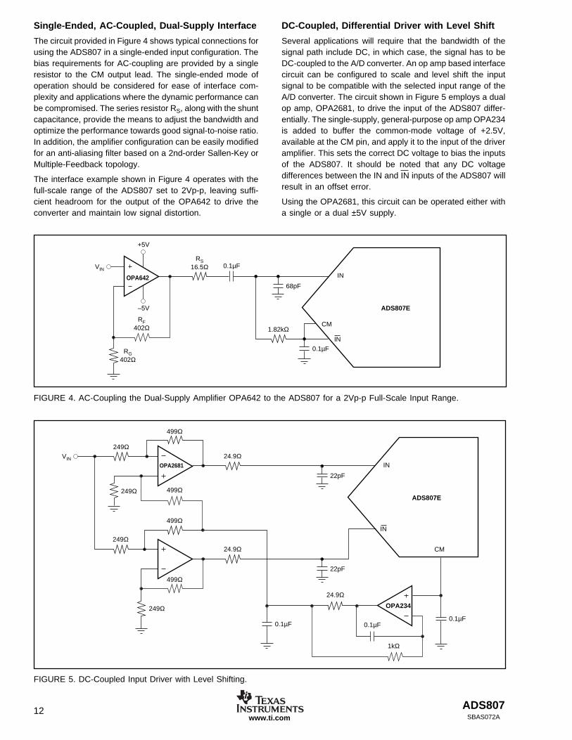
The circuit provided in Figure 4 shows typical connections forusing the ADS807 in a single-ended input configuration. Thebias requirements for AC-coupling are provided by a singleresistor to the CM output lead. The single-ended mode ofoperation should be considered for ease of interface com-plexity and applications where the dynamic performance canbe compromised. The series resistor RS, along with the shuntcapacitance, provide the means to adjust the bandwidth andoptimize the performance towards good signal-to-noise ratio.In addition, the amplifier configuration can be easily modifiedfor an anti-aliasing filter based on a 2nd-order Sallen-Key orMultiple-Feedback topology.
The interface example shown in Figure 4 operates with thefull-scale range of the ADS807 set to 2Vp-p, leaving suffi-cient headroom for the output of the OPA642 to drive theconverter and maintain low signal distortion.
DC-Coupled, Differential Driver with Level Shift
Several applications will require that the bandwidth of thesignal path include DC, in which case, the signal has to beDC-coupled to the A/D converter. An op amp based interfacecircuit can be configured to scale and level shift the inputsignal to be compatible with the selected input range of theA/D converter. The circuit shown in Figure 5 employs a dualop amp, OPA2681, to drive the input of the ADS807 differ-entially. The single-supply, general-purpose op amp OPA234is added to buffer the common-mode voltage of +2.5V,available at the CM pin, and apply it to the input of the driveramplifier. This sets the correct DC voltage to bias the inputsof the ADS807. It should be noted that any DC voltagedifferences between the IN and IN inputs of the ADS807 willresult in an offset error.
Using the OPA2681, this circuit can be operated either witha single or a dual ±5V supply.
FIGURE 4. AC-Coupling the Dual-Supply Amplifier OPA642 to the ADS807 for a 2Vp-p Full-Scale Input Range.
FIGURE 5. DC-Coupled Input Driver with Level Shifting.
VIN
ADS807E
IN
IN
CM
499Ω
249Ω24.9Ω
24.9Ω
249Ω
OPA2681
0.1µF0.1µF 0.1µF
499Ω
499Ω
499Ω
249Ω
249Ω
24.9Ω
1kΩ
22pF
22pF
OPA234
ADS807 13SBAS072A www.ti.com
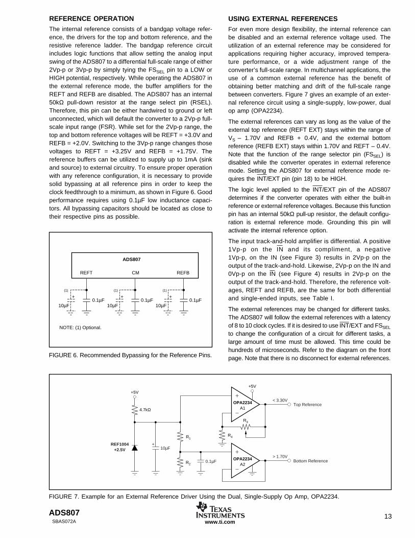
REFERENCE OPERATION
The internal reference consists of a bandgap voltage refer-ence, the drivers for the top and bottom reference, and theresistive reference ladder. The bandgap reference circuitincludes logic functions that allow setting the analog inputswing of the ADS807 to a differential full-scale range of either2Vp-p or 3Vp-p by simply tying the FSSEL pin to a LOW orHIGH potential, respectively. While operating the ADS807 inthe external reference mode, the buffer amplifiers for theREFT and REFB are disabled. The ADS807 has an internal50kΩ pull-down resistor at the range select pin (RSEL).Therefore, this pin can be either hardwired to ground or leftunconnected, which will default the converter to a 2Vp-p full-scale input range (FSR). While set for the 2Vp-p range, thetop and bottom reference voltages will be REFT = +3.0V andREFB = +2.0V. Switching to the 3Vp-p range changes thosevoltages to REFT = +3.25V and REFB = +1.75V. Thereference buffers can be utilized to supply up to 1mA (sinkand source) to external circuitry. To ensure proper operationwith any reference configuration, it is necessary to providesolid bypassing at all reference pins in order to keep theclock feedthrough to a minimum, as shown in Figure 6. Goodperformance requires using 0.1µF low inductance capaci-tors. All bypassing capacitors should be located as close totheir respective pins as possible.
USING EXTERNAL REFERENCES
For even more design flexibility, the internal reference canbe disabled and an external reference voltage used. Theutilization of an external reference may be considered forapplications requiring higher accuracy, improved tempera-ture performance, or a wide adjustment range of theconverter’s full-scale range. In multichannel applications, theuse of a common external reference has the benefit ofobtaining better matching and drift of the full-scale rangebetween converters. Figure 7 gives an example of an exter-nal reference circuit using a single-supply, low-power, dualop amp (OPA2234).
The external references can vary as long as the value of theexternal top reference (REFT EXT) stays within the range ofVS – 1.70V and REFB + 0.4V, and the external bottomreference (REFB EXT) stays within 1.70V and REFT – 0.4V.Note that the function of the range selector pin (FSSEL) isdisabled while the converter operates in external referencemode. Setting the ADS807 for external reference mode re-quires the INT/EXT pin (pin 18) to be HIGH.
The logic level applied to the INT/EXT pin of the ADS807determines if the converter operates with either the built-inreference or external reference voltages. Because this functionpin has an internal 50kΩ pull-up resistor, the default configu-ration is external reference mode. Grounding this pin willactivate the internal reference option.
The input track-and-hold amplifier is differential. A positive1Vp-p on the IN and its compliment, a negative1Vp-p, on the IN (see Figure 3) results in 2Vp-p on theoutput of the track-and-hold. Likewise, 2Vp-p on the IN and0Vp-p on the IN (see Figure 4) results in 2Vp-p on theoutput of the track-and-hold. Therefore, the reference volt-ages, REFT and REFB, are the same for both differentialand single-ended inputs, see Table I.
The external references may be changed for different tasks.The ADS807 will follow the external references with a latencyof 8 to 10 clock cycles. If it is desired to use INT/EXT and FSSEL
to change the configuration of a circuit for different tasks, alarge amount of time must be allowed. This time could behundreds of microseconds. Refer to the diagram on the frontpage. Note that there is no disconnect for external references.
FIGURE 7. Example for an External Reference Driver Using the Dual, Single-Supply Op Amp, OPA2234.
REFT CM
0.1µF
(1) (1) (1)
REFB
ADS807
0.1µF 0.1µF10µF
NOTE: (1) Optional.
+
10µF
+
10µF
+
FIGURE 6. Recommended Bypassing for the Reference Pins.
OPA2234A1
OPA2234A2
R3
R4
R2
R1
+5V+5V
0.1µF
10µF
> 1.70V
< 3.30VTop Reference
Bottom Reference
+
4.7kΩ
REF1004+2.5V
ADS80714SBAS072Awww.ti.com
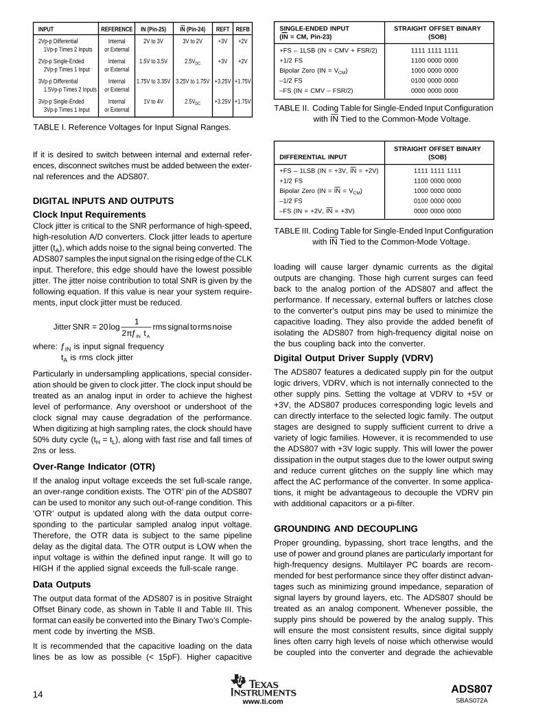
INPUT REFERENCE IN (Pin-25) IN (Pin-24) REFT REFB
2Vp-p Differential Internal 2V to 3V 3V to 2V +3V +2V1Vp-p Times 2 Inputs or External
2Vp-p Single-Ended Internal 1.5V to 3.5V 2.5VDC +3V +2V2Vp-p Times 1 Input or External
3Vp-p Differential Internal 1.75V to 3.35V 3.25V to 1.75V +3.25V +1.75V1.5Vp-p Times 2 Inputs or External
3Vp-p Single-Ended Internal 1V to 4V 2.5VDC +3.25V +1.75V3Vp-p Times 1 Input or External
TABLE III. Coding Table for Single-Ended Input Configurationwith IN Tied to the Common-Mode Voltage.
TABLE II. Coding Table for Single-Ended Input Configurationwith IN Tied to the Common-Mode Voltage.
If it is desired to switch between internal and external refer-ences, disconnect switches must be added between the exter-nal references and the ADS807.
DIGITAL INPUTS AND OUTPUTS
Clock Input RequirementsClock jitter is critical to the SNR performance of high-speed,high-resolution A/D converters. Clock jitter leads to aperturejitter (tA), which adds noise to the signal being converted. TheADS807 samples the input signal on the rising edge of the CLKinput. Therefore, this edge should have the lowest possiblejitter. The jitter noise contribution to total SNR is given by thefollowing equation. If this value is near your system require-ments, input clock jitter must be reduced.
Jitter SNRt
rms signal tormsnoiseIN A
=ƒ
201
2log
πwhere: ƒIN is input signal frequency
tA is rms clock jitter
Particularly in undersampling applications, special consider-ation should be given to clock jitter. The clock input should betreated as an analog input in order to achieve the highestlevel of performance. Any overshoot or undershoot of theclock signal may cause degradation of the performance.When digitizing at high sampling rates, the clock should have50% duty cycle (tH = tL), along with fast rise and fall times of2ns or less.
Over-Range Indicator (OTR)
If the analog input voltage exceeds the set full-scale range,an over-range condition exists. The ‘OTR’ pin of the ADS807can be used to monitor any such out-of-range condition. This‘OTR’ output is updated along with the data output corre-sponding to the particular sampled analog input voltage.Therefore, the OTR data is subject to the same pipelinedelay as the digital data. The OTR output is LOW when theinput voltage is within the defined input range. It will go toHIGH if the applied signal exceeds the full-scale range.
Data Outputs
The output data format of the ADS807 is in positive StraightOffset Binary code, as shown in Table II and Table III. Thisformat can easily be converted into the Binary Two’s Comple-ment code by inverting the MSB.
It is recommended that the capacitive loading on the datalines be as low as possible (< 15pF). Higher capacitive
SINGLE-ENDED INPUT STRAIGHT OFFSET BINARY(IN = CM, Pin-23) (SOB)
+FS – 1LSB (IN = CMV + FSR/2) 1111 1111 1111
+1/2 FS 1100 0000 0000
Bipolar Zero (IN = VCM) 1000 0000 0000
–1/2 FS 0100 0000 0000
–FS (IN = CMV – FSR/2) 0000 0000 0000
STRAIGHT OFFSET BINARYDIFFERENTIAL INPUT (SOB)
+FS – 1LSB (IN = +3V, IN = +2V) 1111 1111 1111
+1/2 FS 1100 0000 0000
Bipolar Zero (IN = IN = VCM) 1000 0000 0000
–1/2 FS 0100 0000 0000
–FS (IN = +2V, IN = +3V) 0000 0000 0000
TABLE I. Reference Voltages for Input Signal Ranges.
loading will cause larger dynamic currents as the digitaloutputs are changing. Those high current surges can feedback to the analog portion of the ADS807 and affect theperformance. If necessary, external buffers or latches closeto the converter’s output pins may be used to minimize thecapacitive loading. They also provide the added benefit ofisolating the ADS807 from high-frequency digital noise onthe bus coupling back into the converter.
Digital Output Driver Supply (VDRV)
The ADS807 features a dedicated supply pin for the outputlogic drivers, VDRV, which is not internally connected to theother supply pins. Setting the voltage at VDRV to +5V or+3V, the ADS807 produces corresponding logic levels andcan directly interface to the selected logic family. The outputstages are designed to supply sufficient current to drive avariety of logic families. However, it is recommended to usethe ADS807 with +3V logic supply. This will lower the powerdissipation in the output stages due to the lower output swingand reduce current glitches on the supply line which mayaffect the AC performance of the converter. In some applica-tions, it might be advantageous to decouple the VDRV pinwith additional capacitors or a pi-filter.
GROUNDING AND DECOUPLING
Proper grounding, bypassing, short trace lengths, and theuse of power and ground planes are particularly important forhigh-frequency designs. Multilayer PC boards are recom-mended for best performance since they offer distinct advan-tages such as minimizing ground impedance, separation ofsignal layers by ground layers, etc. The ADS807 should betreated as an analog component. Whenever possible, thesupply pins should be powered by the analog supply. Thiswill ensure the most consistent results, since digital supplylines often carry high levels of noise which otherwise wouldbe coupled into the converter and degrade the achievable
ADS807 15SBAS072A www.ti.com
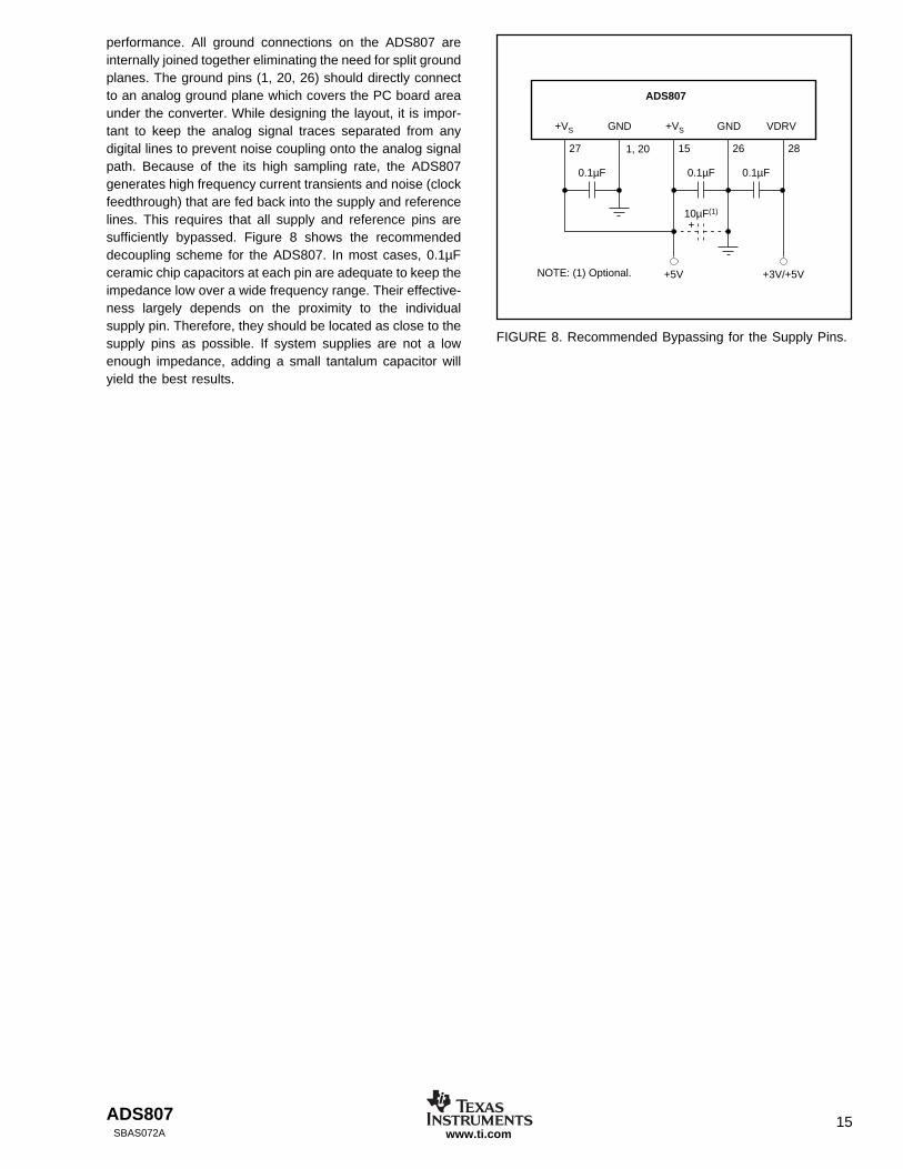
FIGURE 8. Recommended Bypassing for the Supply Pins.
performance. All ground connections on the ADS807 areinternally joined together eliminating the need for split groundplanes. The ground pins (1, 20, 26) should directly connectto an analog ground plane which covers the PC board areaunder the converter. While designing the layout, it is impor-tant to keep the analog signal traces separated from anydigital lines to prevent noise coupling onto the analog signalpath. Because of the its high sampling rate, the ADS807generates high frequency current transients and noise (clockfeedthrough) that are fed back into the supply and referencelines. This requires that all supply and reference pins aresufficiently bypassed. Figure 8 shows the recommendeddecoupling scheme for the ADS807. In most cases, 0.1µFceramic chip capacitors at each pin are adequate to keep theimpedance low over a wide frequency range. Their effective-ness largely depends on the proximity to the individualsupply pin. Therefore, they should be located as close to thesupply pins as possible. If system supplies are not a lowenough impedance, adding a small tantalum capacitor willyield the best results.
0.1µF
NOTE: (1) Optional.
0.1µF
10µF(1)
+5V +3V/+5V
0.1µF
+VS +VSGND
1, 2027 15 26
GND VDRV
28
ADS807
+
PACKAGE OPTION ADDENDUM
www.ti.com 10-Dec-2020
Addendum-Page 1
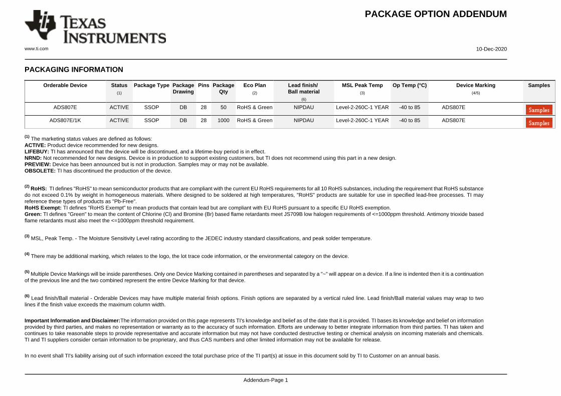
PACKAGING INFORMATION
Orderable Device Status(1)
Package Type PackageDrawing
Pins PackageQty
Eco Plan(2)
Lead finish/Ball material
(6)
MSL Peak Temp(3)
Op Temp (°C) Device Marking(4/5)
Samples
ADS807E ACTIVE SSOP DB 28 50 RoHS & Green NIPDAU Level-2-260C-1 YEAR -40 to 85 ADS807E
ADS807E/1K ACTIVE SSOP DB 28 1000 RoHS & Green NIPDAU Level-2-260C-1 YEAR -40 to 85 ADS807E
(1) The marketing status values are defined as follows:ACTIVE: Product device recommended for new designs.LIFEBUY: TI has announced that the device will be discontinued, and a lifetime-buy period is in effect.NRND: Not recommended for new designs. Device is in production to support existing customers, but TI does not recommend using this part in a new design.PREVIEW: Device has been announced but is not in production. Samples may or may not be available.OBSOLETE: TI has discontinued the production of the device.
(2) RoHS: TI defines "RoHS" to mean semiconductor products that are compliant with the current EU RoHS requirements for all 10 RoHS substances, including the requirement that RoHS substancedo not exceed 0.1% by weight in homogeneous materials. Where designed to be soldered at high temperatures, "RoHS" products are suitable for use in specified lead-free processes. TI mayreference these types of products as "Pb-Free".RoHS Exempt: TI defines "RoHS Exempt" to mean products that contain lead but are compliant with EU RoHS pursuant to a specific EU RoHS exemption.Green: TI defines "Green" to mean the content of Chlorine (Cl) and Bromine (Br) based flame retardants meet JS709B low halogen requirements of <=1000ppm threshold. Antimony trioxide basedflame retardants must also meet the <=1000ppm threshold requirement.
(3) MSL, Peak Temp. - The Moisture Sensitivity Level rating according to the JEDEC industry standard classifications, and peak solder temperature.
(4) There may be additional marking, which relates to the logo, the lot trace code information, or the environmental category on the device.
(5) Multiple Device Markings will be inside parentheses. Only one Device Marking contained in parentheses and separated by a "~" will appear on a device. If a line is indented then it is a continuationof the previous line and the two combined represent the entire Device Marking for that device.
(6) Lead finish/Ball material - Orderable Devices may have multiple material finish options. Finish options are separated by a vertical ruled line. Lead finish/Ball material values may wrap to twolines if the finish value exceeds the maximum column width.
Important Information and Disclaimer:The information provided on this page represents TI's knowledge and belief as of the date that it is provided. TI bases its knowledge and belief on informationprovided by third parties, and makes no representation or warranty as to the accuracy of such information. Efforts are underway to better integrate information from third parties. TI has taken andcontinues to take reasonable steps to provide representative and accurate information but may not have conducted destructive testing or chemical analysis on incoming materials and chemicals.TI and TI suppliers consider certain information to be proprietary, and thus CAS numbers and other limited information may not be available for release.
In no event shall TI's liability arising out of such information exceed the total purchase price of the TI part(s) at issue in this document sold by TI to Customer on an annual basis.
PACKAGE OPTION ADDENDUM
www.ti.com 10-Dec-2020
Addendum-Page 2
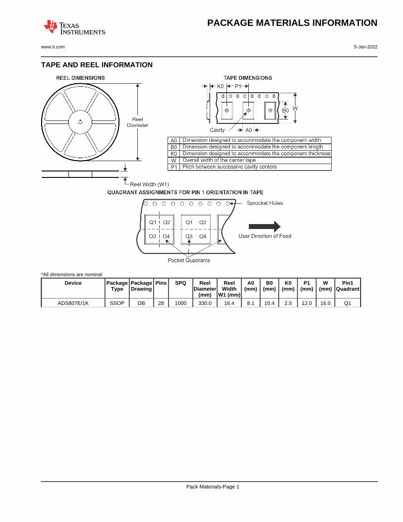
TAPE AND REEL INFORMATION
*All dimensions are nominal
Device PackageType
PackageDrawing
Pins SPQ ReelDiameter
(mm)
ReelWidth
W1 (mm)
A0(mm)
B0(mm)
K0(mm)
P1(mm)
W(mm)
Pin1Quadrant
ADS807E/1K SSOP DB 28 1000 330.0 16.4 8.1 10.4 2.5 12.0 16.0 Q1
PACKAGE MATERIALS INFORMATION
www.ti.com 5-Jan-2022
Pack Materials-Page 1
*All dimensions are nominal
Device Package Type Package Drawing Pins SPQ Length (mm) Width (mm) Height (mm)
ADS807E/1K SSOP DB 28 1000 853.0 449.0 35.0
PACKAGE MATERIALS INFORMATION
www.ti.com 5-Jan-2022
Pack Materials-Page 2
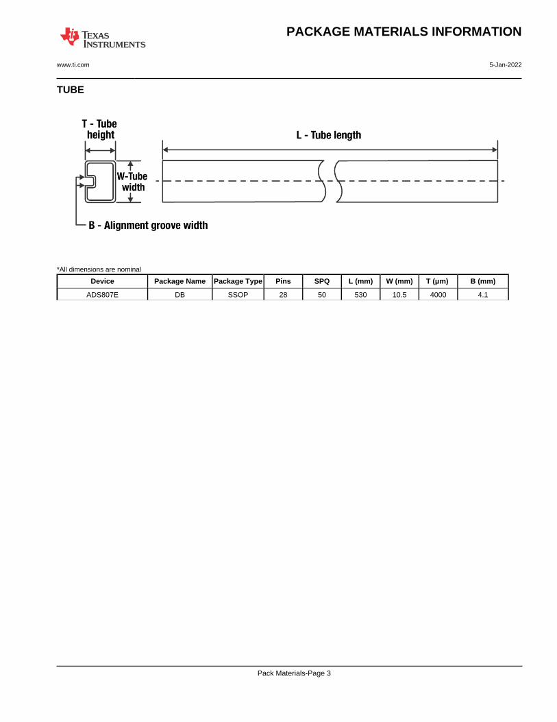
TUBE
*All dimensions are nominal
Device Package Name Package Type Pins SPQ L (mm) W (mm) T (µm) B (mm)
ADS807E DB SSOP 28 50 530 10.5 4000 4.1
PACKAGE MATERIALS INFORMATION
www.ti.com 5-Jan-2022
Pack Materials-Page 3
www.ti.com
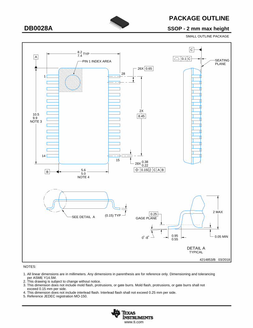
PACKAGE OUTLINE
C
26X 0.65
2X8.45
28X 0.380.22
8.27.4 TYP
SEATINGPLANE
0.05 MIN
0.25GAGE PLANE
0 -8
2 MAX
B 5.65.0
NOTE 4
A
10.59.9
NOTE 3
0.950.55
(0.15) TYP
SSOP - 2 mm max heightDB0028ASMALL OUTLINE PACKAGE
4214853/B 03/2018
1
1415
28
0.15 C A B
PIN 1 INDEX AREA
SEE DETAIL A
0.1 C
NOTES: 1. All linear dimensions are in millimeters. Any dimensions in parenthesis are for reference only. Dimensioning and tolerancing per ASME Y14.5M. 2. This drawing is subject to change without notice. 3. This dimension does not include mold flash, protrusions, or gate burrs. Mold flash, protrusions, or gate burrs shall not exceed 0.15 mm per side. 4. This dimension does not include interlead flash. Interlead flash shall not exceed 0.25 mm per side.5. Reference JEDEC registration MO-150.
A 15DETAIL ATYPICAL
SCALE 1.500
www.ti.com
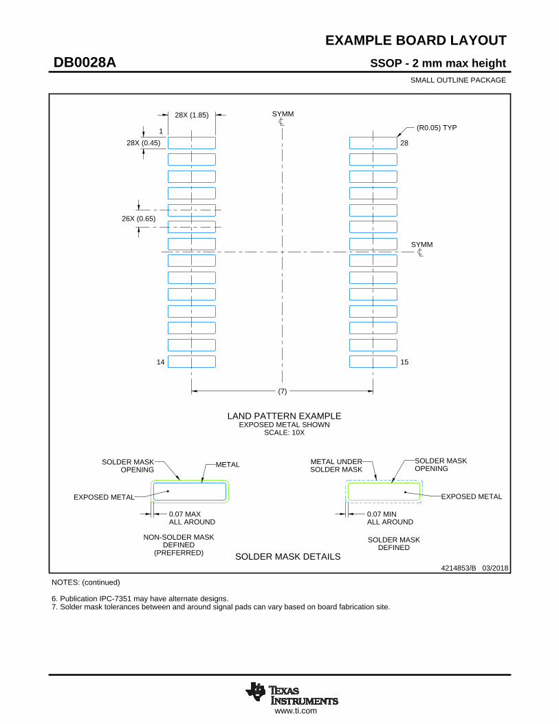
EXAMPLE BOARD LAYOUT
0.07 MAXALL AROUND
0.07 MINALL AROUND
28X (1.85)
28X (0.45)
26X (0.65)
(7)
(R0.05) TYP
SSOP - 2 mm max heightDB0028ASMALL OUTLINE PACKAGE
4214853/B 03/2018
NOTES: (continued) 6. Publication IPC-7351 may have alternate designs. 7. Solder mask tolerances between and around signal pads can vary based on board fabrication site.
LAND PATTERN EXAMPLEEXPOSED METAL SHOWN
SCALE: 10X
SYMM
SYMM
1
14 15
28
15.000
METALSOLDER MASKOPENING
METAL UNDERSOLDER MASK
SOLDER MASKOPENING
EXPOSED METALEXPOSED METAL
SOLDER MASK DETAILS
NON-SOLDER MASKDEFINED
(PREFERRED)
SOLDER MASKDEFINED
www.ti.com
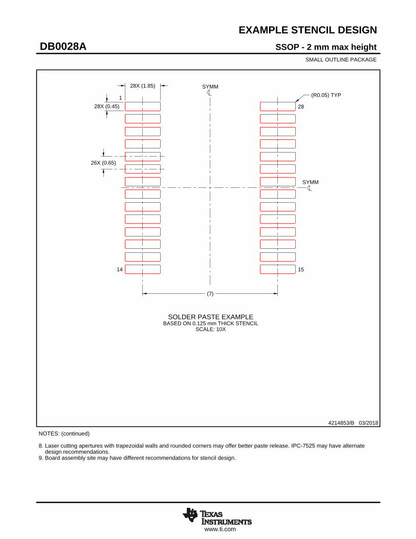
EXAMPLE STENCIL DESIGN
28X (1.85)
28X (0.45)
26X (0.65)
(7)
(R0.05) TYP
SSOP - 2 mm max heightDB0028ASMALL OUTLINE PACKAGE
4214853/B 03/2018
NOTES: (continued) 8. Laser cutting apertures with trapezoidal walls and rounded corners may offer better paste release. IPC-7525 may have alternate design recommendations. 9. Board assembly site may have different recommendations for stencil design.
SOLDER PASTE EXAMPLEBASED ON 0.125 mm THICK STENCIL
SCALE: 10X
SYMM
SYMM
1
14 15
28

IMPORTANT NOTICE AND DISCLAIMERTI PROVIDES TECHNICAL AND RELIABILITY DATA (INCLUDING DATA SHEETS), DESIGN RESOURCES (INCLUDING REFERENCE DESIGNS), APPLICATION OR OTHER DESIGN ADVICE, WEB TOOLS, SAFETY INFORMATION, AND OTHER RESOURCES “AS IS” AND WITH ALL FAULTS, AND DISCLAIMS ALL WARRANTIES, EXPRESS AND IMPLIED, INCLUDING WITHOUT LIMITATION ANY IMPLIED WARRANTIES OF MERCHANTABILITY, FITNESS FOR A PARTICULAR PURPOSE OR NON-INFRINGEMENT OF THIRD PARTY INTELLECTUAL PROPERTY RIGHTS.These resources are intended for skilled developers designing with TI products. You are solely responsible for (1) selecting the appropriate TI products for your application, (2) designing, validating and testing your application, and (3) ensuring your application meets applicable standards, and any other safety, security, regulatory or other requirements.These resources are subject to change without notice. TI grants you permission to use these resources only for development of an application that uses the TI products described in the resource. Other reproduction and display of these resources is prohibited. No license is granted to any other TI intellectual property right or to any third party intellectual property right. TI disclaims responsibility for, and you will fully indemnify TI and its representatives against, any claims, damages, costs, losses, and liabilities arising out of your use of these resources.TI’s products are provided subject to TI’s Terms of Sale or other applicable terms available either on ti.com or provided in conjunction with such TI products. TI’s provision of these resources does not expand or otherwise alter TI’s applicable warranties or warranty disclaimers for TI products.TI objects to and rejects any additional or different terms you may have proposed. IMPORTANT NOTICE
Mailing Address: Texas Instruments, Post Office Box 655303, Dallas, Texas 75265Copyright © 2022, Texas Instruments Incorporated